Article

A Miniaturized and Fast System for Thin Film Thickness Measurement

State Key Laboratory of Precision Measuring Technology & Instruments, Centre of MicroNano Manufacturing Technology, Tianjin University, Tianjin 300072, China
*
Author to whom correspondence should be addressed.
Appl. Sci. 2020, 10(20), 7284; https://doi.org/10.3390/app10207284
Submission received: 25 August 2020 / Revised: 13 October 2020 / Accepted: 15 October 2020 / Published: 18 October 2020
(This article belongs to the Section Applied Physics General)

Abstract

:
Transparent films are significant industrial components that are widely used in modern optics, microelectronics, optical engineering, and other related fields. There is an urgent need for the fast and stable thickness measurement of industrial films at the micron-grade. This paper built a miniaturized and low-cost film thickness measurement system based on confocal spectral imaging and the principle of thin-film spectral interference. The reflection interference spectrum was analyzed to extract the phase term introduced by the film thickness from the full spectrum information, where local spectral noise can be better corrected. An efficient and robust film thickness calculation algorithm was realized without any calibrating sample. The micron-grade thickness measurement system had an industrial property with a measurement range of up to 75 μm with a measurement uncertainty of 0.1 μm, presenting a good performance in single-layer film thickness measurement with high efficiency.

1. Introduction

Transparent film, as an important industrial component, is widely used in modern optics, microelectronics, optical engineering, and other related scientific and technological fields. Various films produced by physical or chemical deposition methods can use interference effects to change optical properties, such as antireflection, filtering, and polarization. Meanwhile, their protection characteristics such as high-temperature resistance, corrosion, and abrasion play a decisive role in the quality of optical instruments in the fields of communication, display, storage, etc. [1,2] However, film preparation is affected by process parameters such as emission characteristics, relative position placement, and surface shape of the plated parts, resulting in uneven thickness distribution, which affects the barrier performance and tensile properties of subsequent applications [3]. Therefore, the measurement and evaluation of film thickness are particularly important in the production process, especially for the thickness measurement of micron-grade industrial films. Limited by the irregular industrial environment, there is an urgent need for a fast, stable, and robust high-resolution film thickness measurement system.
Based on the characteristics of light absorption, reflection, and polarization, the optical measurement methods of film thickness can be divided into spectrophotometry [4,5], ellipsometry [6,7,8], interferometry [9,10,11], and multiple compound methods [12,13,14]. Although the measurement methods based on ellipsometry and interferometry have high resolution and accuracy, the disadvantages of large system size, high price, and strict environmental conditions do not meet the rapid and stable application requirement of industrial measurement. The spectrophotometry is more widely used due to its simplicity and portability. Spectral reflectometry is an effective means to detect the thickness of the weakly absorbing film in spectrophotometry. Reflectometry has less affection than transmittance by extinction coefficient [15] and can realize the compound assembly of the signal transmitter and receiver due to optical fiber technology, thus avoiding the alignment problem. The film thickness calculation methods based on the reflection spectrum can be subdivided into the envelope method [5], the full-spectrum fitting method [16], the turning point fitting method, etc. The above methods all use the reflectivity curve as the medium to obtain the film thickness indirectly. Therefore, the system is required to have a high stability light source or a high-precision reference sample. Second, these methods depend greatly on the reflectivity model, which means that non-ideal signals containing noise in actual measurements are prone to distortion. Among them, the envelope method, fitting the upper and lower envelope by the extreme points of the reflectivity curve, is easily affected by the baseline drift under temperature changes; for the full spectrum fitting method, the period and amplitude of the full-spectrum reflectance spectrum are matched at the same time, which may lead to over-fitting and low matching efficiency; only a very few wavelength data with an odd multiple of the optical thickness λ/4 is used in the turning point fitting method. The effective data segment needs to be selected manually, which makes it difficult to achieve automatic measurement.
According to the current research on thin-film thickness measurement, the existing methods still have disadvantages such as poor robustness, low efficiency, and high cost, which cannot meet the needs of industrial-grade rapid and stable measurement. Therefore, this paper built a miniaturized and rapid film thickness measurement system based on the principle of film low-coherence interference and confocal spectral imaging. A novel algorithm named phase power spectrum (PPS) analysis was proposed to calculate the film thickness by solving the power spectral density of the phase term. With no need for reference sample correction, the film thickness measurement system had the performance of a measurement range of 1–75 μm, measurement uncertainty of 0.1 μm, and measurement speed of 10 ms. The efficient and stable film thickness calculation of the standard films with micron-grade thickness, the film layer on the PCB chip, and the Germanium-based lens verified the feasibility of this method.

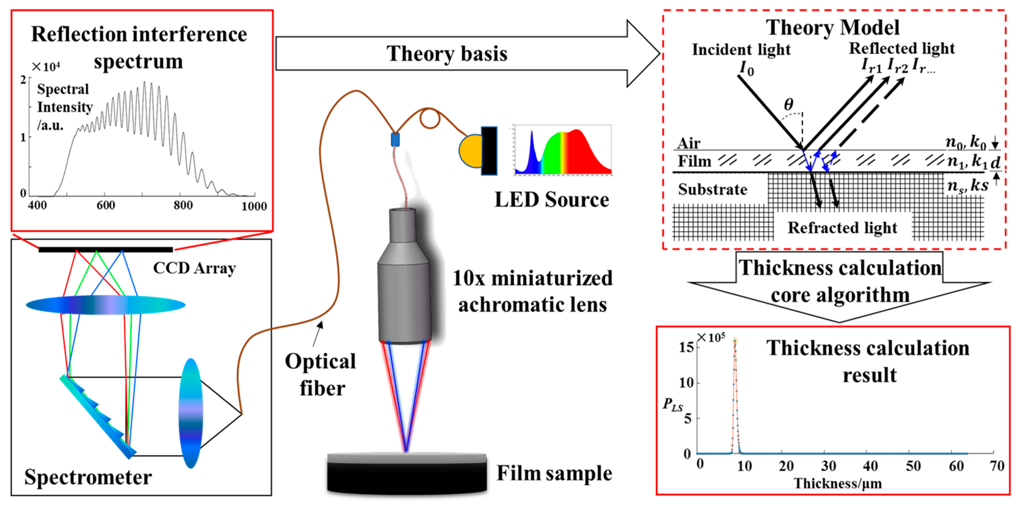
2. Measurement Scheme

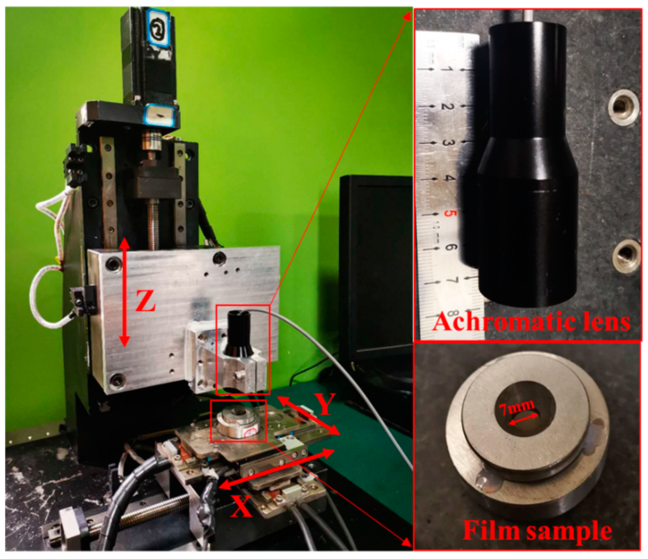
Based on the principle of thin-film interference and confocal spectral imaging, this paper built a low-cost and fast-speed thin-film thickness measurement system to study the thickness calculation algorithm of the thin film. As shown in Figure 1, a Light Emitting Diode (LED), a micro-spectrometer, and a self-designed confocal achromatic probe are used to realize the miniaturization of the measurement system.
The light intensity changes periodically in a coherent region with destructive and constructive phenomena. For dielectric films, if the absorption of light by the film is not considered, the total interference intensity of the reflected light beam incident on the film can be approximately expressed as
I r ( z , λ ) = I r 1 + I r 2 + 2 I r 1 I r 2 cos ( 2 π z / λ + ϕ 0 )   =   I 0 ( λ ) R 01 + I 0 ( λ ) T 01 R 1 s T 10 + 2 I 0 ( λ ) R 01 T 01 R 1 s T 10 cos ( 2 π z / λ + ϕ 0 )
where λ is the wavelength and ϕ0 is the additional phase. R01 and T01, respectively, represent the reflectance and transmittance from the air to the film. R1s and T10, respectively, represent the reflectance from the film to the substrate and the transmittance from the film to the air. For the case of normal incidence, the optical path difference z = 2n1 × d is determined by the film’s refractive index n1 and thickness d, where the refractive index is treated as a constant to improve computational efficiency.
The envelope of the spectral interference signal measured by the spectrometer is approximately a Gaussian distribution. The phase term 2πz/λ + ϕ0 caused by the optical path difference z determines the density of the interference fringes. As the core algorithm of the PPS analysis, Empirical Mode Decomposition (EMD) and Lomb–Scargle periodogram (LSP) process the high-frequency spectral interference information successively to extract the film thickness.

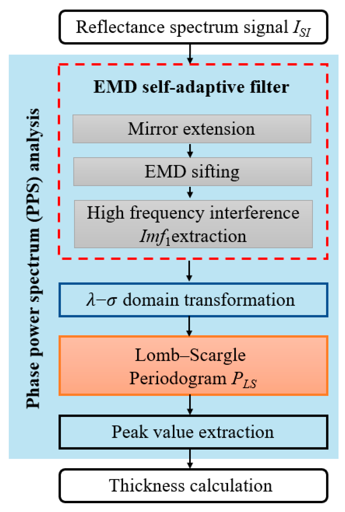
3. Film Thickness Calculation Algorithm

Figure 2 is the flow chart of the core algorithm in this paper. Firstly, aiming at the original interference signal collected by a spectrometer, EMD is used as a high-pass filter to extract high-frequency interference components, adaptively eliminating the influence of the non-uniform intensity distribution of the LED source. Second, to obtain the phase term introduced by film thickness, the interference component is transformed into the wavenumber σ domain through reciprocal of wavelength λ. Third, through the spectral analysis method, we extract the phase term from the full spectrum to effectively avoid the interference of local noise. However, conventional spectral analysis methods, such as Fourier transform, cannot handle the problem of non-equal interval sampling of signals caused by the λ−σ transformation. In this paper, the phase term is solved by the LSP spectrum analysis and illustrated by phase power spectral density distribution. Finally, the peak value of the power spectral density function is extracted by the maximum value method to calculate the film thickness. The detailed flow of the proposed algorithm is as follows.
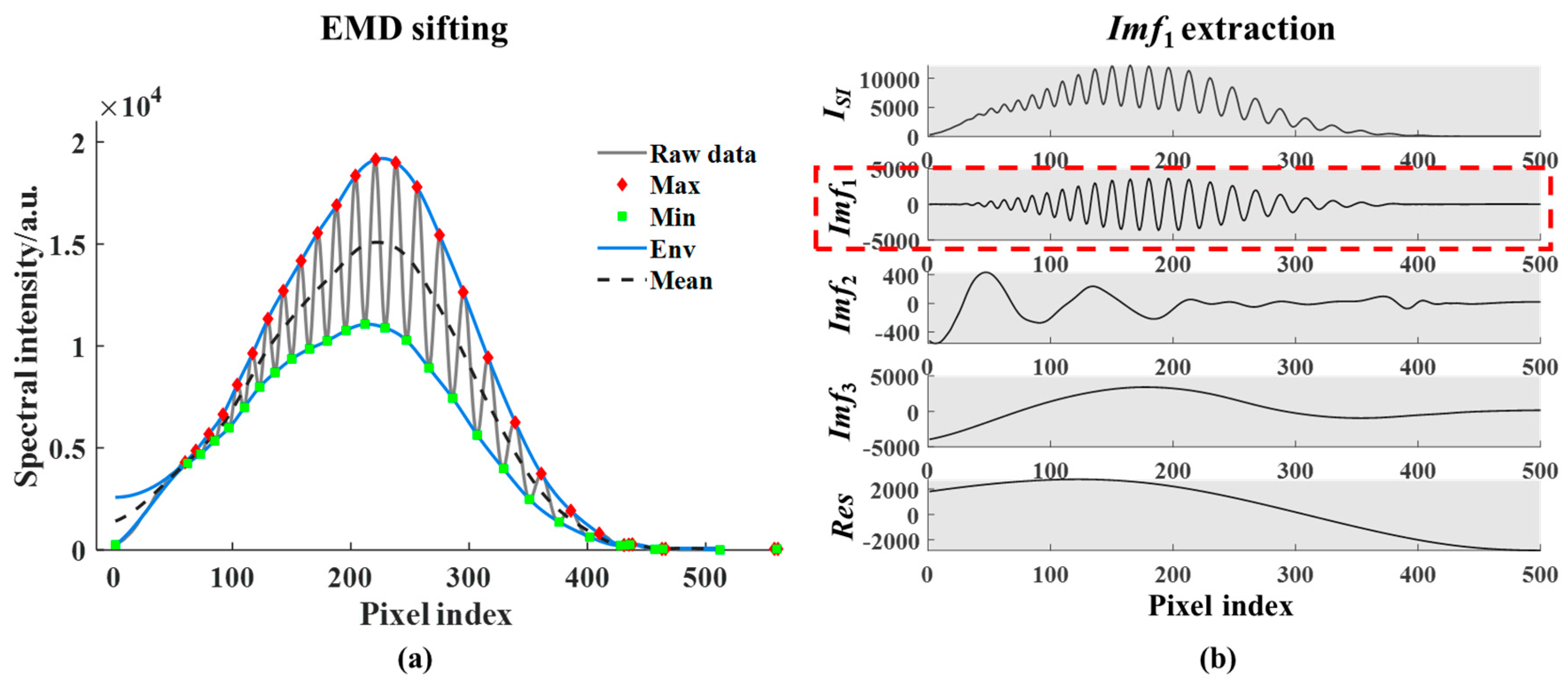
EMD, as the preprocessing algorithm of Hilbert Huang Transform (HHT) [17], can adaptively decompose the complex nonlinear and non-stationary signal into a limited number of Intrinsic Mode Function (IMF). In this paper, EMD is used as a high-pass filter [18] to automatically filter out the high-frequency principal component of the reflectance spectrum signal. The mirror extending method [19] assists in processing the endpoint data of the original signal to eliminate the boundary oscillation effect caused by the third-order spline interpolation in EMD.
The reflectance spectrum signal ISI is a discrete function of the uniform sampled pixels for being collected by Charge Coupled Device (CCD) array in a micro spectrometer. After EMD filtering, ISI is disassembled into a set of IMF components Imfk, k = 1, 2, …, m of different frequency ranges, and a monotonic trend function Res, as shown in Figure 3b. Imf1 is the first component to be filtered out with the highest signal frequency. In the case with no high-frequency noise, Imf1 is the film interference principal component. Then, according to the corresponding relationship between the pixel index and the wavelength of CCD array in the spectrometer, the intensity Ii of each σi, i = 1, 2, …, N, is obtained by converting Imf1 from the λ to the σ domain. N is the number of pixels of the spectrometer.
Due to the wavelength drift of the spectrometer and the reciprocal transformation from the λ to the σ domain, the non-uniform sampled characteristic of σi made Ii unable to be directly analyzed by the conventional spectral analysis method. Therefore, it is necessary to preprocess Ii before performing spectral analysis to obtain film thickness information We adopt the cubic spline interpolation combined fast Fourier transform (CIFFT) and LSP [20,21] as two representative methods to process Ii, and finally choose the LSP after comparing the solution results. In particular, inspired by the time-frequency domain (tf) transformation [22], we rewrite the LSP function into the wavenumber-phase factor domain (σ−z) transformation form, as Equations (2) and (3).
P L S ( z ) = 1 2 { [ i = 1 N I i cos ( 2 π z ( σ i δ ) ) ] 2 i = 1 N cos 2 ( 2 π z ( σ i δ ) ) + [ i = 1 N I i sin ( 2 π z ( σ i δ ) ) ] 2 i = 1 N sin 2 ( 2 π z ( σ i δ ) ) }
where δ is specified for each z to ensure time-shift invariance,
δ = 1 4 π z tan 1 ( i = 1 N sin ( 4 π z σ i ) i = 1 N cos ( 4 π z σ i ) )
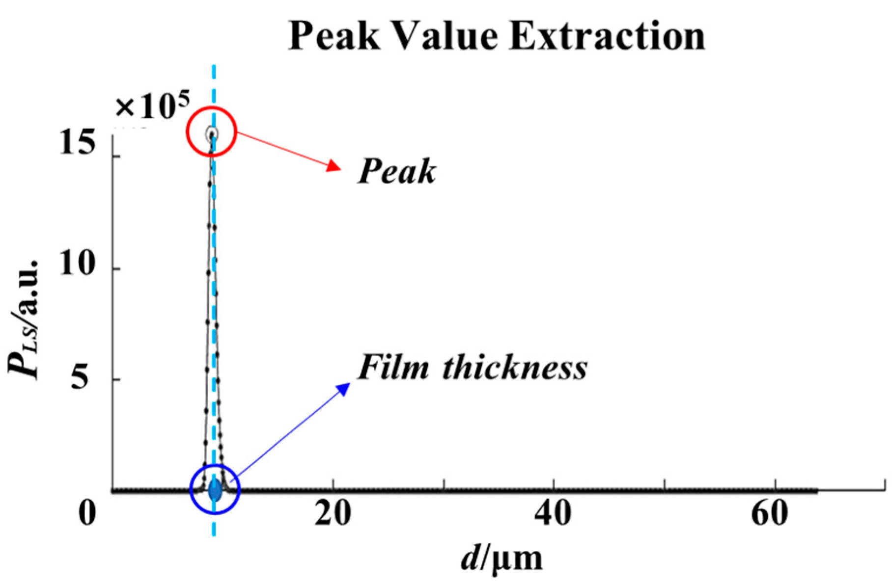
Under normal circumstances, the full width at half maximum of the single-layer film interference spectrum after LSP transformation is small (30–50 nm) as shown in Figure 4. Therefore, the peak value zpeak can be directly extracted by the maximum value method. The built-in false alarm probability of LSP evaluates the significance of the peak value to further ensure the correct extraction. If n1 is the refractive index of the film, the film thickness d is
d = z p e a k / 2 n 1
In the PPS algorithm, EMD as a self-adaptive high-pass filter realizes the non-destructive extraction of spectral interference terms. While expanding the measurement range of the film, it effectively reduces the influence of the non-uniform distribution of the light source spectrum. The essence of LSP is to fit the data with a single sine function y = acos (ωt) + bsin (ωt) with the same frequency [20], which implicitly requiring the mean value of the measurement data to be zero. The IMF components after EMD filtering approximately meet this requirement, thus the combination of EMD and LSP can obtain a significant deterministic solution. Besides, LSP uses full range spectrum data and thus can better correct the gross errors introduced by local spectral noise. At the same time, using the built-in statistical tool of LSP to evaluate the reliability of the solution can greatly eliminate the false frequency interference caused by environmental noise and improve the stability of the system.

4. Simulation

The following problems have been found in the actual measurement of various types of films. (1) The absorption and reflection coefficients varying with film materials, which results in different fringe contrast of the actual film interference signal; (2) the influence of external stray light causes local noise in the reflected spectrum signal, which have an impact on the film thickness calculation. Besides, to clarify the effective range, inherent error, and the feasibility of this system, we conduct a simulation analysis based on the thin-film interference model. By adjusting the fringe contrast, the thickness, and the noise of the interference signal, we clarify the error influence of different measurement conditions, thus verify the robustness of the algorithm.

4.1. Verification of the Thin-Film Interference Model

We use the thin-film interference model Ir (z, λ) of Equation (1) for simulation, where A = R01 + T01R1sT10, B = 2 R 01 T 01 R 1 s T 10 , A, B∈(0,1], and suppose the light source intensity distribution conforms to the Gaussian distribution G(λ; μ, η2) with mathematical expectation μ and standard variance η2,
G ( λ ; μ , η 2 ) = 1 η 2 π e ( λ μ ) 2 2 η 2
The reflected spectrum signal can be abbreviated as below, where C is the maximum intensity amplitude of the light spectrum,
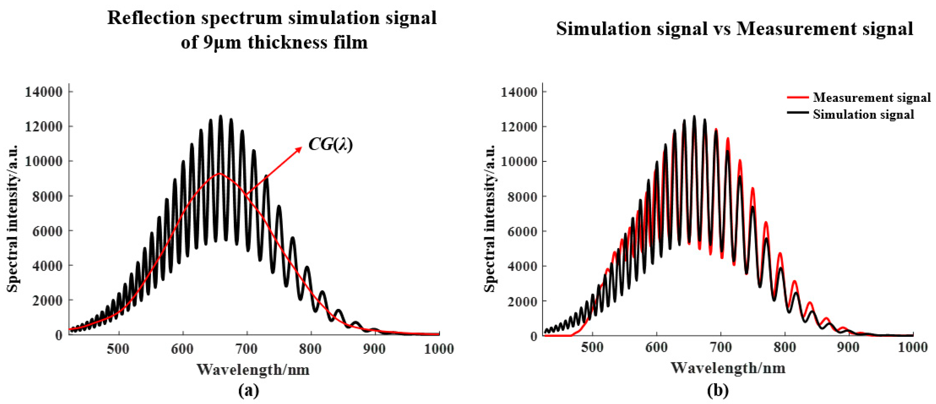
I r ( z , λ ) = ( A + B cos ( 2 π z / λ + ϕ 0 ) ) C G ( λ )
We take A = 0.5, B = 0.2, C = 18000, μ = 660 nm, η = 80 nm, ϕ0 = π, and z = 9 μm. The simulated interference spectrum is shown in Figure 5a and compared with the measured data in Figure 5b. The simulation signal is consistent with the actual measurement signal, which verifies the correctness of the simulation model.

4.2. Correlation Analysis of Influencing Factors

4.2.1. Influence of Thin-Film Thickness

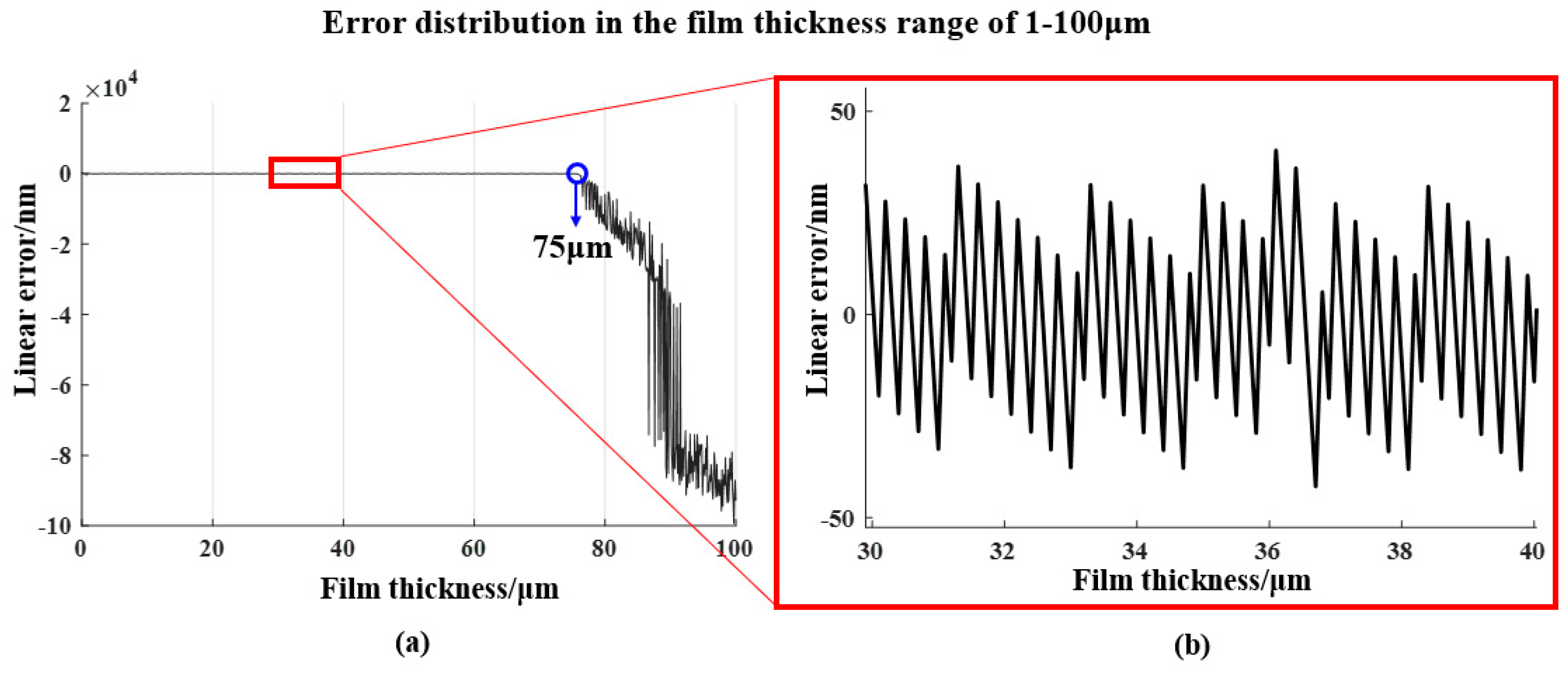
Using 0.1 μm as the interval of thickness value in Ir (z, λ) to simulate the reflection spectrum of 1–100 μm film. The simulation result in Figure 6 shows the inherent error of the algorithm changes periodically within ±50 nm in the effective range of 1–75 μm. The current measurement range is also limited by the wavelength resolution of the spectrometer, resulting in the failure calculation of the film thickness over 75 μm.

4.2.2. Influence of Thin-Film Materials

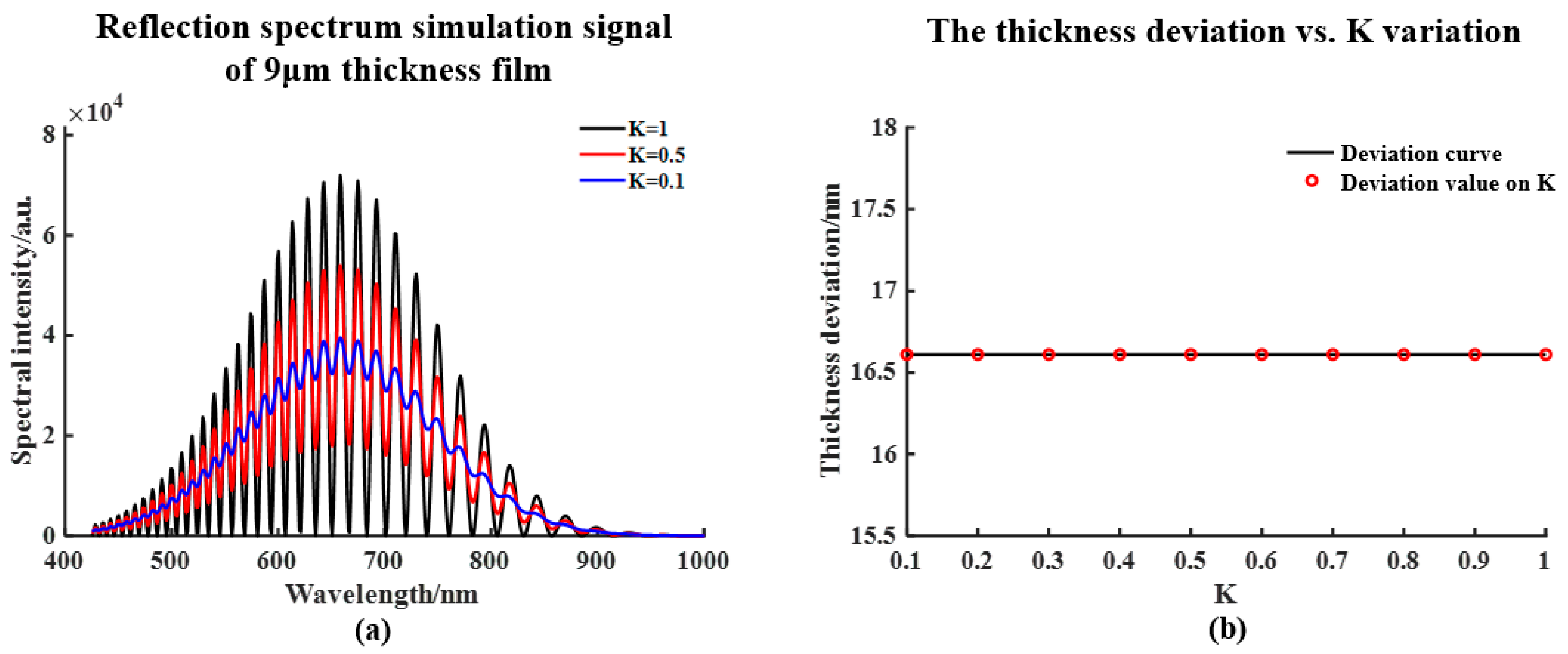
Based on the simulation signal of Ir (z, λ), we change signal contrast K = B/A to analyze the influence caused by various absorption and reflection coefficients under different film materials. Figure 7a illustrates the reflection spectrum signals with of 0.1, 0.5, and 1, respectively. For a particular thickness, the amplitude of the signal gets higher when contrast increases, while the period remains nearly constant. The thickness calculation deviations under different contrasts are shown in Figure 7b. The deviations keep the value of 16.61 nm, which proves that the interference signal contrast does not relate to the thickness calculation deviation.

4.2.3. Influence of Noise

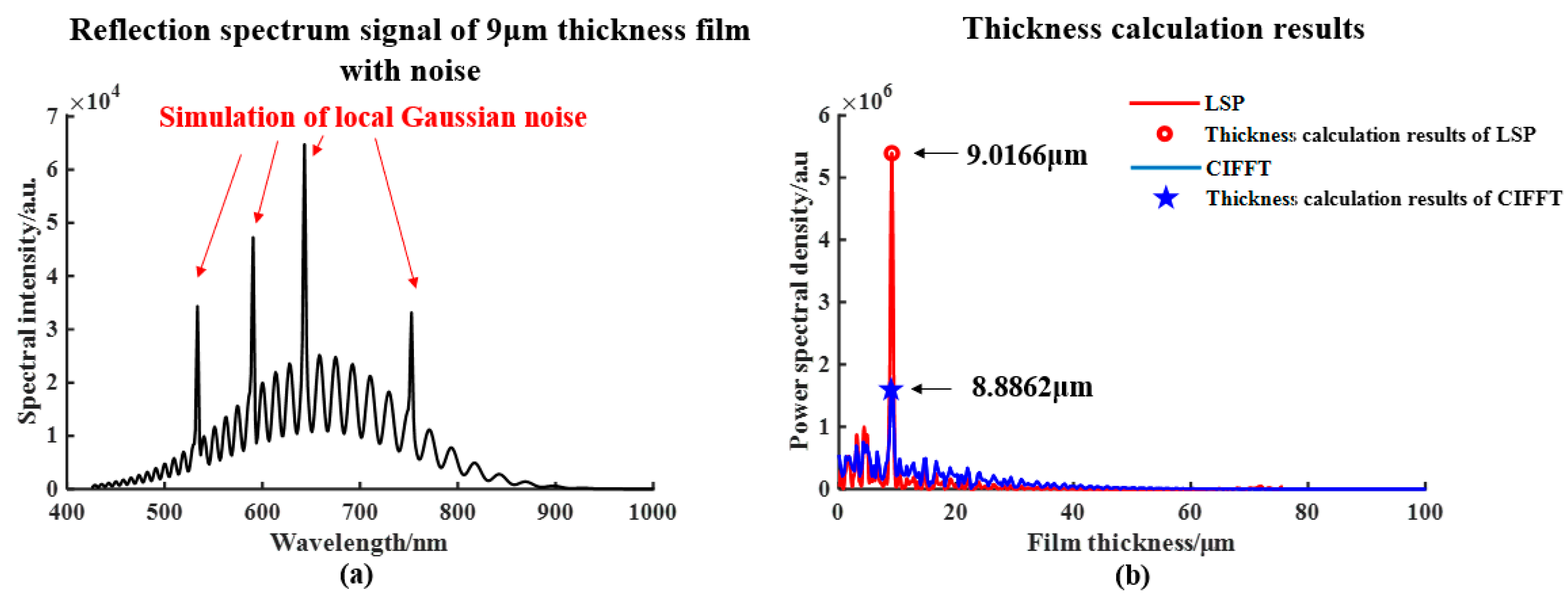
Irregular local Gaussian noise is added to the basic interference signal based on Ir (z, λ) to simulate the noise introduced by CCD pixel data packet loss or environmental vibration to verify the robustness of the algorithm. As shown in 
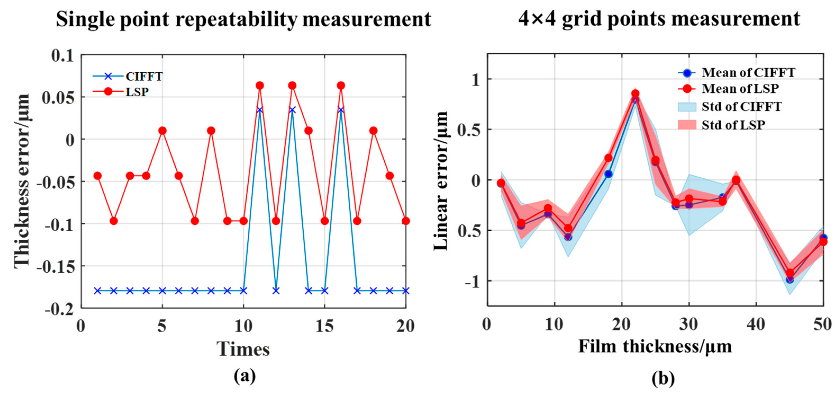
Figure 8b, the calculation result of LSP is closer to the true value of the thickness than CIFFT. Although the noise components are still contained in power spectrum density, whose density is much smaller compared to the peak value especially after LSP. Therefore, the combination of EMD and LSP has sufficient robustness by reducing the misjudgment rate.

5. Experiments and Discussion

To verify the correctness and effectiveness of the proposed algorithm, this paper built a miniaturized thin film thickness measurement system as shown in Figure 9. The experimental system consists of a three-axis translation stage, a commercial fiber spectrometer, and a self-developed small achromatic microscope probe. The probe is mounted on the Z-axis guide rail and the Z-axis guide rail is fixed on the XY table. The X, Y, and Z-axis guide rails drive the translation and lifting of the probe, to realize the rapid and high-precision scanning measurement of the film sample.
To ensure the measurement accuracy of the system, the experiment performs wavelength calibration on the spectrometer and eliminate high-order diffraction by measuring the spectral line of a mercury-argon standard light source in the range of 300–1000 nm. The standard wavelength values of the characteristic spectral line of the light source are provided by the National Institute of Standards and Technology (NIST) [23]. The corresponding relationship between the wavelength and the index of each CCD pixel is obtained by the second-order fitting.

5.1. Thin-Film Thickness Uncertainty Verification

5.1.1. Standard Film Samples Measurement

A set of Polyvinyl chloride (PVC) standard film samples with a thickness range of 2–50 (±0.3 + 0.5% H) μm are fixed by a custom film clamping device as shown in Figure 9. First, we measure the standard film of 18 μm thickness at a random point for 20 times to verify the single point repeatability of the system. After EMD filtering, CIFFT and LSP algorithms are adopted to calculate the thickness, respectively. As shown in Figure 10a, the measurement result indicates that the thickness deviation of LSP fluctuates in the range of ±0.1 μm. The mean deviation of LSP is −0.038 μm, while the mean deviation of CIFFT is −0.147 μm. Comparing to CIFFT, LSP has a lower uncertainty and a smaller deviation for film thickness, which proves that the system has good repeatability in the single-point thickness measurement. Secondly, to further verify the stability of the area measurement of the experimental system, we measure 16 signals in different areas in a circular hole with a diameter of 7 mm in the standard film sample group. The measurement results of the 4 × 4 grid uniformly distributed sampling points are shown in Figure 10b. The center point of the error bar and the longitudinal length of the shaded area represent the mean and standard deviation of the measurement error related to the standard value, respectively. The maximum absolute error of LSP is 0.9202 μm, and the repeatability is no more than 2.5%. The experiment result proves that the proposed PPS algorithm is stable and reliable and meets industrial requirement repeatability. The average calculation time is 0.01 s for each measurement. Due to the anisotropic tensile forces in the clamping process of the standard film, the wrinkles and uneven thickness distribution of film are inevitable, which causes the measurement results of several film thicknesses in this experiment to be too large. Overall, the measurement uncertainty of the PPS algorithm proposed in this paper is stable at 0.1 μm.

5.1.2. Germanium-Based 1 μm SiO2 Standard Film Measurement

Germanium is the most widely used infrared optical material and often covered with a thin film to enhance the transmittance and durability in harsh environments such as high temperature and acid. In this article, a 1 μm thickness SiO2 film sample on a germanium substrate with a stepped structure is measured to verify the accuracy of thickness control during the coating process. In Figure 11a, the stepped structure consists of an uncoated area, and a coated area is designed for the measurement benchmark and measured by white light interference (WLI) 12 times. At the same time, the PPS performs a 12 points measurement on the coating part of the WLI measurement area.
After leveling and denoising, the vertical distance between the upper and lower fitting surfaces of the step shown in Figure 11b, is calculated to represent the WLI measurement result. The detailed measurement result is shown in Table 1. Comparing the PPS and WLI measurement data, the mean thickness of PPS is 0.892 μm and the standard deviation is 0.076 μm, while the mean thickness of WLI is 0.954 μm, and the standard deviation is 0.053 μm. The mean of PPS measurement results is about 50nm smaller than WLI, but the measurement speed is faster than WLI.

5.2. Measurement Experiment of PCB Chip Film Thickness

To protect the key chips on semiconductor PCB, the surface is generally treated with coating or glue. The coating thickness is various in a different area, thus fast and non-destructive measurement has important engineering value. This paper aims at the needs of industrial PCB chip transparent film thickness measurement and uses the method to carry out experimental verification. For different areas of the PCB board, the transparent film with 1–30 μm thickness is measured multiple times. In Figure 12, the measurement results at three points a, b, and c on the different electronic chips are 2.067 μm, 3.515 μm, and 24.910 μm, respectively, which match the reference values 2 μm, 3.5 μm, and 25 μm provided by the factory. The absolute thickness errors are 67 nm, 15 nm, and 90 nm, respectively.

6. Conclusions

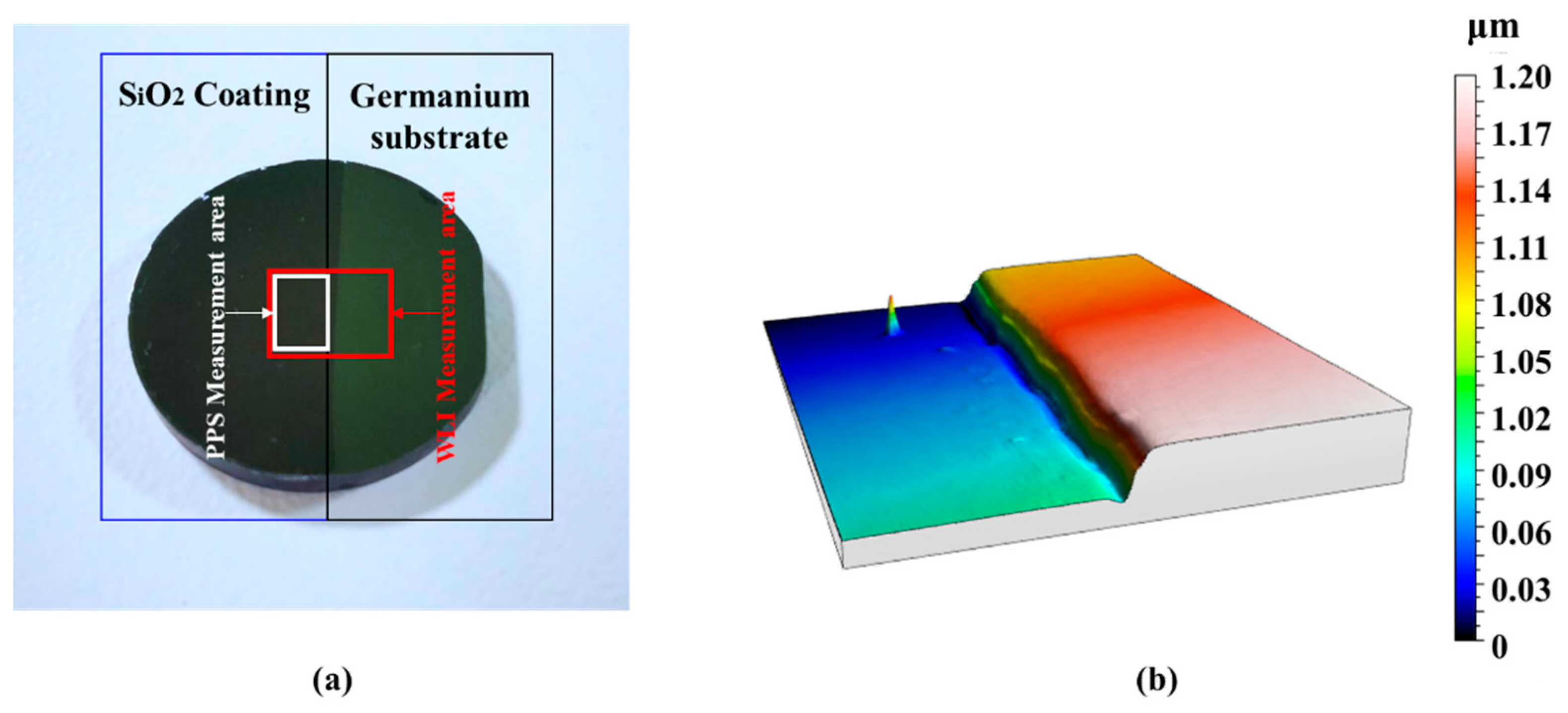
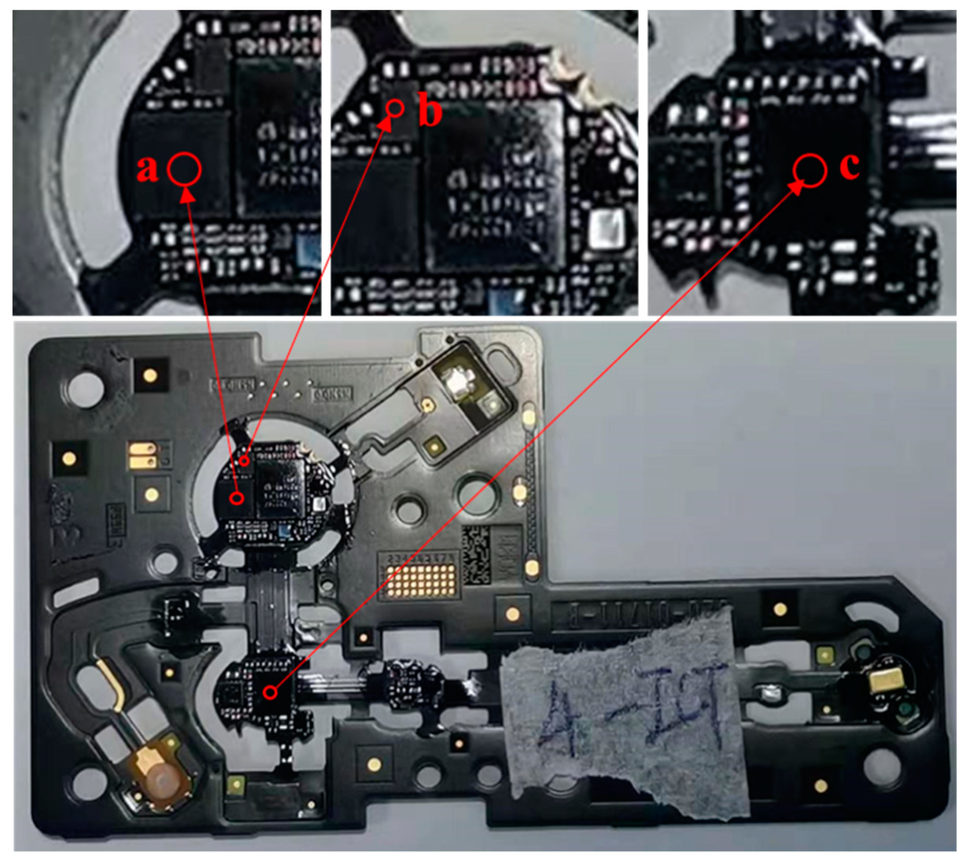
Based on the reflection spectrum interference theory, this paper built a low-cost and miniaturized thin-film thickness measurement system with the measurement range of 1–75 μm, an angle of ±5°, and an uncertainty of 0.1 μm. The measurement speed of 10 ms and no need of focusing within millimeter working distance met the efficient and convenient requirements of industrial-grade measurement. The validity of the system was verified by experiments of the standard PVC films, the micron-grade film layer on PCB chip, and Germanium-based SiO2 film. In the proposed phase power spectrum analysis method, the high-frequency spectral interference term was extracted adaptively from the full spectrum data through loop iterations, avoiding the use of the reference sample. For single-layer film thickness measurement, power spectrum analysis resolved the film thickness from the spectral interference term and corrected the gross error caused by local spectral noise, thereby ensuring the stability of the algorithm.
It is also clear that the industrial film thickness measurement results in this article need to be further optimized due to the lack of hardware performance. In the following work, the measurement range can be increased by selecting a high-resolution spectrometer. We can continue to optimize the algorithm model and the probe design to further improve the uncertainty of the measurement system.

Author Contributions

Funding acquisition, F.F. and X.Z.; methodology, R.H.; project administration, X.Z.; supervision, L.Z.; writing—original draft, R.H.; writing—review & editing, L.Z. and Z.L. All authors discussed the results and agreed to the published version of the manuscript.

Funding

This research was funded by the National Key Research and Development Program of China (Grant No. 2017YFA0701200), the Science Challenge Program (Grant No. TZ2018006-0203-01), the Tianjin Natural Science Foundation of China (Grant No. 19JCZDJC39100), and the Postdoctoral Innovative Talent Support Program of China (BX20190230).

Acknowledgments

The authors express their sincere thanks to Yiting Duan, Yongbin Lu, and Boyang Shi for the preparation of the experiment and valuable discussions.

Conflicts of Interest

The authors declare no conflict of interest.

References

  1. Karim, A. Thin Film Heater for Removable Volatile Protecting Coatings. Sci. World J. 2013, 2013, 1–3. [Google Scholar] [CrossRef] [PubMed] [Green Version]
  2. Hu, S.; Lewis, N.S.; Ager, J.W.; Yang, J.; McKone, J.R.; Strandwitz, N.C. Thin-Film Materials for the Protection of Semiconducting Photoelectrodes in Solar-Fuel Generators. J. Phys. Chem. C 2015, 119, 24201–24228. [Google Scholar] [CrossRef]
  3. Abadias, G.; Chason, E.; Keckes, J.; Sebastiani, M.; Thompson, G.B.; Barthel, E.; Doll, G.L.; Murray, C.E.; Stoessel, C.H.; Martinu, L. Review Article: Stress in thin films and coatings: Current status, challenges, and prospects. J. Vac. Sci. Technol. A 2018, 36, 020801. [Google Scholar] [CrossRef] [Green Version]
  4. Yang, M.; Gatto, A.; Kaiser, N. Optical thin films with high reflectance, low thickness and low stress for the spectral range from vacuum UV to near IR. J. Opt. A Pure Appl. Opt. 2006, 8, 327–332. [Google Scholar] [CrossRef]
  5. Luňáček, J.; Hlubina, P.; Lunácková, M. Simple method for determination of the thickness of a nonabsorbing thin film using spectral reflectance measurement. Appl. Opt. 2009, 48, 985–989. [Google Scholar] [CrossRef] [PubMed]
  6. Pristinski, D.; Kozlovskaya, V.; Sukhishvili, S.A. Determination of film thickness and refractive index in one measurement of phase-modulated ellipsometry. J. Opt. Soc. Am. A 2006, 23, 2639–2644. [Google Scholar] [CrossRef]
  7. Nestler, P.; Helm, C.A. Determination of refractive index and layer thickness of nm-thin films via ellipsometry. Opt. Express 2017, 25, 27077–27085. [Google Scholar] [CrossRef]
  8. Li, D.; Song, X.; Xu, J.; Wang, Z.; Zhang, R.; Zhou, P.; Zhang, H.; Huang, R.; Wang, S.; Zheng, Y.; et al. Optical properties of thickness-controlled MoS2 thin films studied by spectroscopic ellipsometry. Appl. Surf. Sci. 2017, 421, 884–890. [Google Scholar] [CrossRef]
  9. Ghim, Y.-S.; Kim, Y.-J. Thin-film thickness profile and its refractive index measurements by dispersive white-light interferometry. Opt. Express 2006, 14, 11885–11891. [Google Scholar] [CrossRef] [PubMed]
  10. Guo, T.; Chen, Z.; Li, M.; Wu, J.; Fu, X.; Hu, X. Film thickness measurement based on nonlinear phase analysis using a Linnik microscopic white-light spectral interferometer. Appl. Opt. 2018, 57, 2955–2961. [Google Scholar] [CrossRef]
  11. Park, J.; Kim, J.-A.; Ahn, H.; Bae, J.; Jin, J. A Review of Thickness Measurements of Thick Transparent Layers Using Optical Interferometry. Int. J. Precis. Eng. Manuf. 2019, 20, 463–477. [Google Scholar] [CrossRef]
  12. Hlubina, P.; Luňáček, J.; Ciprian, D.; Chlebus, R. Spectral interferometry and reflectometry used to measure thin films. Appl. Phys. A 2008, 92, 203–207. [Google Scholar] [CrossRef] [Green Version]
  13. Zhou, Y.; Wu, G.S.; Dai, W.; Li, H.B.; Wang, A.Y. Accurate determination of optical constants and thickness of absorbing thin films by a combined ellipsometry and spectrophotometry approach. Acta Phys. Sin. Ch. Ed. 2010, 59, 2356–2363. [Google Scholar] [CrossRef]
  14. Taudt, C.; Preuß, M.; Nelsen, B.; Baselt, T.; Koch, E.; Hartmann, P. Thin-film characterization with a dual-channel dispersion-encoded imaging low-coherence interferometry approach. Proc. Spie 2019, 10925, 109250L. [Google Scholar] [CrossRef]
  15. Tang, J.F.; Gu, P.F.; Liu, X.; Li, H.F. Modern Optical Thin Film Technology; Zhejiang University Press: Hangzhou, China, 2006; p. 32. [Google Scholar]
  16. Nečas, D.; Vodák, J.; Ohlídal, I.; Ohlídal, M.; Majumdar, A.; Zajíčková, L. Simultaneous determination of dispersion model parameters and local thickness of thin films by imaging spectrophotometry. Appl. Surf. Sci. 2015, 350, 149–155. [Google Scholar] [CrossRef]
  17. Huang, N.E.; Shen, Z.; Long, S.R.; Wu, M.C.; Shih, H.H.; Zheng, Q.; Yen, N.-C.; Tung, C.C.; Liu, H.H. The empirical mode decomposition and the Hilbert spectrum for nonlinear and non-stationary time series analysis. Proc. R. Soc. A Math. Phys. Eng. Sci. 1998, 454, 903–995. [Google Scholar] [CrossRef]
  18. Flandrin, P.; Rilling, G.; Goncalves, P. Empirical Mode Decomposition as a Filter Bank. IEEE Signal Process. Lett. 2004, 11, 112–114. [Google Scholar] [CrossRef] [Green Version]
  19. Zhao, J.-P. Mirror extending and circular spline function for empirical mode decomposition method. J. Zhejiang Univ. A 2001, 2, 247–252. [Google Scholar] [CrossRef]
  20. Lomb, N.R. Least-squares frequency analysis of unequally spaced data. Astrophys. Space Sci. 1976, 39, 447–462. [Google Scholar] [CrossRef]
  21. Scargle, J.D. Studies in astronomical time series analysis. II—Statistical aspects of spectral analysis of unevenly spaced data. Astrophys. J. 1982, 263, 835–853. [Google Scholar] [CrossRef]
  22. Vanderplas, J. Understanding the Lomb–Scargle Periodogram. Astrophys. J. Suppl. Ser. 2018, 236, 16. [Google Scholar] [CrossRef]
  23. Nair, R.V.; Vijaya, R. Multiple Bragg diffraction in polymeric photonic crystals. Appl. Opt. 2009, 48, G59–G63. [Google Scholar] [CrossRef] [PubMed]
Figure 1. Schematic diagram of the thin-film thickness measurement principle.
Applsci 10 07284 g001
Figure 2. Flowchart of the proposed phase power spectrum (PPS) algorithm.
Applsci 10 07284 g002
Figure 3. Empirical Mode Decomposition (EMD) high-pass filtering process. (a) EMD sifting process; (b) Intrinsic Mode Function (IMF) components of different frequency ranges.
Applsci 10 07284 g003
Figure 4. Peak extraction and film thickness calculation.
Applsci 10 07284 g004
Figure 5. The 9 μm thickness film interference simulation diagram. (a) Simulation diagram of reflection spectrum under Gaussian light source; (b) Comparison of reflection spectrum simulation and measurement signal.
Applsci 10 07284 g005
Figure 6. The influence of thin-film thickness on the calculation error. (a) Error distribution in the film thickness range of 1–100 μm. (b) Error within effective range fluctuates periodically within 50 nm.
Applsci 10 07284 g006
Figure 7. The influence of interference fringe contrast on the calculated thickness deviation. (a) The reflection spectrum simulation signal of 9 μm thickness film when the contrast K is 0.1, 0.5, and 1. (b) The thickness deviation vs. K variation.
Applsci 10 07284 g007
Figure 8. The influence of local Gaussian noise on the calculated thickness deviation. (a) Reflection spectrum signal including local Gaussian noise of 9 μm thickness film. (b) Power spectral density and power spectrum calculated using Lomb–Scargle periodogram (LSP) and cubic spline interpolation combined fast Fourier transform (CIFFT) respectively membrane thickness.
Applsci 10 07284 g008
Figure 9. Experimental measurement system setup.
Applsci 10 07284 g009
Figure 10. Comparison of the result of CIFFT and LSP algorithm for standard film (a) Single point repeatability measurement; (b) 4 × 4 grid points measurement.
Applsci 10 07284 g010
Figure 11. (a) The SiO2 film with a 1 μm step on the germanium substrate. (b) The three dimensional morphology of step by white light interferometry.
Applsci 10 07284 g011
Figure 12. Measurement experiment of film thickness in different areas on PCB.
Applsci 10 07284 g012
Table 1. PPS and white light interference (WLI) measurement results of germanium-based 1 μm SiO2 standard film.
MethodsPPSWLI
NumberThickness (μm)Deviation (μm)Thickness (μm)Deviation (μm)
10.916−0.0840.835−0.165
20.839−0.1610.901–0.099
30.763−0.2370.913−0.087
40.992−0.0081.0300.030
50.763−0.2370.939−0.061
60.916−0.0840.942−0.058
70.916−0.0840.968−0.032
80.916−0.0840.989−0.011
90.839−0.1611.0100.010
100.839−0.1610.972−0.028
110.916−0.0840.998−0.002
120.992−0.0080.955−0.045
Mean0.8920.954
Standard Deviation0.0760.053
Publisher’s Note: MDPI stays neutral with regard to jurisdictional claims in published maps and institutional affiliations.

