Article

Numerical Simulation of an InP Photonic Integrated Cross-Connect for Deep Neural Networks on Chip

Institute for Photonic Integration, Eindhoven University of Technology, 5600 MB Eindhoven, The Netherlands
*
Author to whom correspondence should be addressed.
Appl. Sci. 2020, 10(2), 474; https://doi.org/10.3390/app10020474
Submission received: 30 November 2019 / Revised: 24 December 2019 / Accepted: 26 December 2019 / Published: 9 January 2020
(This article belongs to the Special Issue Optics for AI and AI for Optics)

Abstract

:
We propose a novel photonic accelerator architecture based on a broadcast-and-weight approach for a deep neural network through a photonic integrated cross-connect. The single neuron and the complete neural network operation are numerically simulated. The weight calibration and weighted addition are reproduced and demonstrated to behave as in the experimental measurements. A dynamic range higher than 25 dB is predicted, in line with the measurements. The weighted addition operation is also simulated and analyzed as a function of the optical crosstalk and the number of input colors involved. In particular, while an increase in optical crosstalk negatively influences the simulated error, a greater number of channels results in better performance. The iris flower classification problem is solved by implementing the weight matrix of a trained three-layer deep neural network. The performance of the corresponding photonic implementation is numerically investigated by tuning the optical crosstalk and waveguide loss, in order to anticipate energy consumption per operation. The analysis of the prediction error as a function of the optical crosstalk per layer suggests that the first layer is essential to the final accuracy. The ultimate accuracy shows a quasi-linear dependence between the prediction accuracy and the errors per layer for a normalized root mean square error lower than 0.09, suggesting that there is a maximum level of error permitted at the first layer for guaranteeing a final accuracy higher than 89%. However, it is still possible to find good local minima even for an error higher than 0.09, due to the stochastic nature of the network we are analyzing. Lower levels of path losses allow for half the power consumption at the matrix multiplication unit, for the same error level, offering opportunities for further improved performance. The good agreement between the simulations and the experiments offers a solid base for studying the scalability of this kind of network.

1. Introduction

The boost in data volume of the information transient and data storage continuously stimulates the demand for high-speed information processing [1,2]. Artificial neural networks (ANNs) are becoming essential for feature extraction [3], image classification [4], time series prediction [5] and system optimization [6] as they are able to extract meaningful information from huge datasets more efficiently. They are also widely adopted by scientific communities to investigate bio-structure prediction [7], astronomical pattern extraction [8], nuclear fusion environment control [9], in telecommunication [10], etc. Novel neural network architectures based on non-von Neuman architectures to perform parallel computation have been demonstrated based on advanced electronics. As some examples, IBM TrueNorth [11], Neurogrid [12], SpiNNaker [13], and BrainDrop [14] are designed for spiking neural networks, while FPGA [15], EIE [16] and Google TPU [17] are for deep neural networks. The level of energy efficiency has been reported to be in the order of a few pJ/operation. However, the computation speed is constrained by the limited bandwidth of the electrical interconnections. Photonics technology provides a promising approach for neural network implementation as it offers parallel information processing when exploiting different domains (wavelength, polarization, phase, space), resulting in ultrabroad bandwidth that outperforms the electronics, while it decouples power consumption from computational speed. Recently, an ultrafast leaky integrate-and-fire neuron with a fiber-based system has been employed for spiking processing [18]. Large-scale optical neural networks using discrete optical components and micro-optics [19] and delay-based recurrent neural networks exploiting laser dynamics [20] have been reported. However, path-dependent and phase difference make the bulky systems difficult to scale up. Today’s photonic integration technology can provide mature miniaturized solutions for high-performance sophisticated integrated circuits [21,22]. A photonic reservoir computing unit has been proposed based on time delays and semiconductor optical amplifiers (SOAs) [23] or Mach–Zehnder interferometers (MZIs) [24] for time-sequential recognition, though they are not programmable as they rely on distributed nonlinearities in the system. A photonic programable feed-forward neural network has been proposed based on a coherent approach using MZI elements [25], in which the optical neuron layer combines serval serial stages, resulting in phase noise accumulation. Micro-ring resonator-based optical neural networks with wavelength division multiplexing (WDM) operation have promised to increase interconnection bandwidth [26], however thermal crosstalk and low dynamic range complicate the weight calibration. Recently we have demonstrated the implementation of a photonic deep neural network (PDNN) via cross-connect circuits based on a broadcast-and-weight architecture, using SOAs and array waveguide gratings (AWGs) [27]. By running an image classification problem, we have demonstrated that an accuracy of up to 85.8% is possible. But, the influence of chip losses and optical crosstalk on the ultimate prediction accuracy has not been investigated yet. This is an important step to make for further improvement and scalability investigation.
In this work, we introduce the cross-connect-based photonic deep neural network and we simulate the matrix multiplication unit (MMU) via the VPIphotonics Design Suit (VPIphotonics, Berlin, Germany) simulation software. In particular, we benchmark the simulation results versus the experimental results to offer a solid platform for further analysis. We study the influence of the optical crosstalk, coming from the AWGs, as well as the impact of the path loss, to identify margins for further scalability per layer and energy saving. The single neuron and complete neural network operation are numerically simulated to provide guidelines on how to design future cross-connect photonic integrated chips for accelerating computation on-chip. In Section 2, we introduce the exploited SOA-based PDNN. The implementation and simulation with an optical cross-connect structure are described in Section 3, while the weighted calibration and neuron-weighted addition are demonstrated in Section 4. The three-layer PDNN is used to solve the image classification problem in Section 5, followed by the conclusions in Section 6.

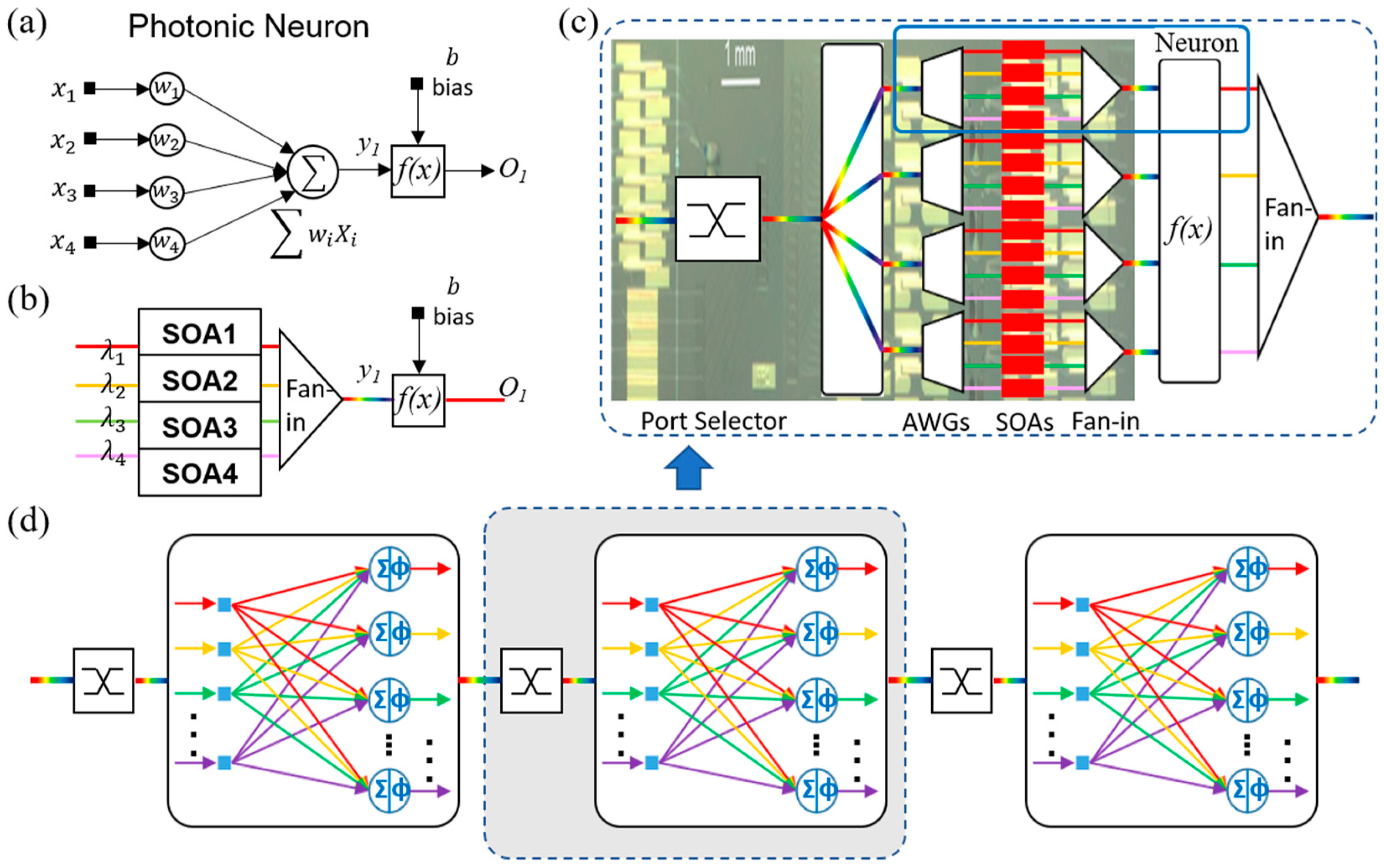
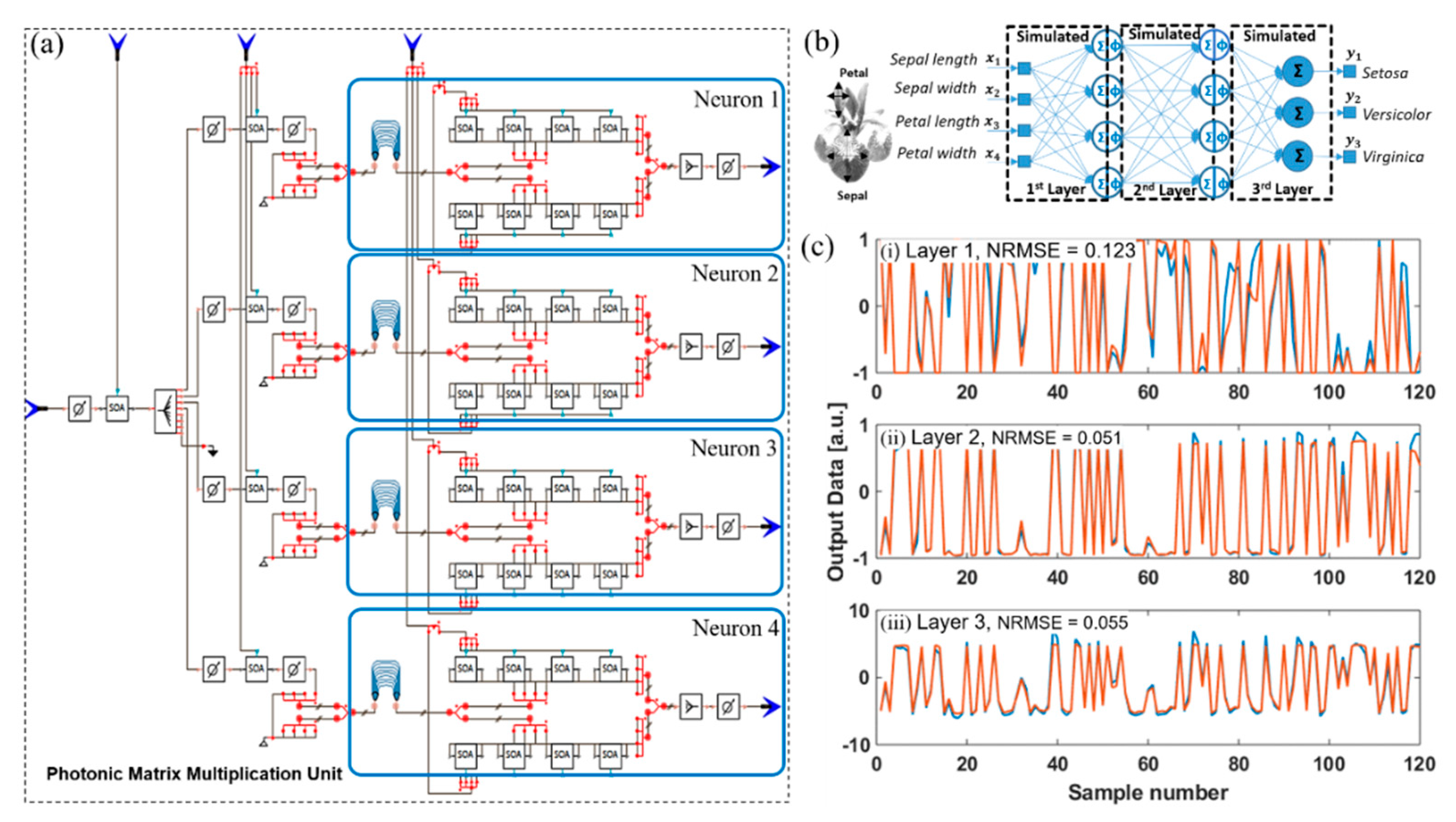
2. Photonic Deep Neural Network with Weight-SOAs

The implementation of deep neural networks via a photonic approach takes advantage of the available parallelism of light beams. Figure 1 depicts the envisaged photonic deep neural network which uses wavelength division multiplexing (WDM) input signals, from the photonic neuron to the large-scale neural network. Here in particular, we realize multiple weighted additions, linear operations in an artificial neuron, via a broadcast-and-weight architecture, which are the most computational heavy elements in the neural network.
The basic element of the neural network is an artificial neuron. Figure 1a depicts the basic neuron model with the output signal being yj = f(∑Wij xi + bj), where f is the activation function, xi is the ith element of the input vector, Wij is the weight factor for the input value xi and bj is the bias in the jth neuron, with the weighted addition given by ∑Wijxi. The output of one full layer of M neurons can be expressed as a vector: y = f(W·x + b), where x is the input vector with N elements, W is the M × N weight matrix, b, a bias vector with M elements, with matrix multiplication W·x. Figure 1b illustrates the corresponding photonic implementation with SOAs. In this instance, the input x is encoded onto several channels at different wavelengths and the individual input is weighted with the given gain/attenuation provided by an SOA. The weighted signals are then combined into a WDM signal and sent to the nonlinear function to provide a single wavelength neuron output. The nonlinear activation function can be realized in several ways, e.g., by employing the combination of a photodetector and a modulator [26], saturable absorbers [25], excitable lasers [28,29], wavelength converters [30], and phase change materials [31]. In this simulation work, we use a photodetector and off-line processing for nonlinear function and we mainly focus on the operation of weighted addition for the matrix multiplication. Utilizing photodetectors at the output of the matrix multiplication, the detected summation of all the weighted signals results in
V = (R·Z0/vπ) ∙ x ∙ exp [h·(I)]
where R is the signal detection response, assumed to be constant for dense WDM signals, Z0 is the PD characteristic impedance and vπ the voltage at π phase shift. The vector h (I) has N elements, the ith element h(Ii) is the gain integrated over the length of the SOA for weighting input xi, where the injection current is Ii. The outputs are then sent to the nonlinear function which processes the signal and produces the outputs of the neuron.
One full neural layer consists of linear matrix multiplications and nonlinear operations. The details of a neuron layer with four neurons, as used in this paper, are illustrated in Figure 1c, where the input WDM signal is selected by using a port selector that directs the desired input signal to this layer to be processed (see chip picture). The input signal is split and sent to the neurons (one neuron highlighted with a blue box). The AWG in the neuron de-multiplexes the input into individual channels, whose weight is assigned with different gains by using different weighted SOAs as shown in Figure 1b. The combined weighted signals from the four output ports pass through the activation function f, which is implemented via software with a hyperbolic tangent function. The output of the nonlinear activation function is a monochromatic wave that carries the information after the nonlinear operation. The outputs from different neurons in this layer are combined to be sent to the next layer of neurons for deeper processing. Figure 1d shows a schematic of the implementation of a full three-layer photonic deep neural network. The input of the neuron layers comes from the combined WDM output from the previous layer. The gray box shows one of the layers of the PDNN. By feeding forward the processed signals, the photonic deep neural network layer is realized. The included port selector may be used to select the desired input source.
To verify this photonic neural network concept, the simulation of the weight tuning and four channel weighted addition of a single photonic neuron is carried out and compared with the experimental results for calibration. The complete three-layer network is then implemented for solving the iris flower classification problem. A detailed analysis of the influence of the optical crosstalk and path losses on the error at each layer and on the final prediction accuracy is also executed to understand opportunities for improvements and scalability.

3. Optical Cross-Connect: Implementation and Simulation

We use VPIphotonics to simulate the integrated cross-connect-based weighted addition as the basic function of the photonic deep neural network. This software allows for numerical modeling of photonic systems as well as of photonic components within the integrated chips and for different material platforms. The simulated set up is built with symbolic blocks and a hierarchal structure. For the passive elements, we execute the simulation in frequency domain, while for the active elements, such as the SOAs, the transmission-line model is applied to model them in time domain [32].
The implemented and simulated setup scheme is showed in Figure 2. Figure 2a is the complete setup scheme for examining our cross-connect photonic integrated chip shown in Figure 1c, with similar operating conditions as in the real experiment, for analyzing the integrated SOA-based PDNN. The photonic integrated chip is an 8 × 8 × 8λ cross-connect, but in the experiments, a WDM input is used which contains 4 channels. An arbitrary waveform generator (detailed scheme shown in Figure 2b) is utilized to generate the electrical signal from the data file at 10 GSymbol/s, with 4 DACs with 8-bit precision. Figure 2c shows 4 lasers and 4 modulators for the optical signal generation of 4 input channels. The WDM input of four channels is generated via these four Mach–Zehnder interferometer-based modulators, with the electrical RF signal coming from the arbitrary waveform generator, and CW lasers at 193.1 THz, 193.5 THz, 193.9 THz, and 194.3 THz. A channel separation of 3.2 nm is used to match the channel separation of the AWG on chip. The input signal is coupled into the photonic matrix multiplication unit (MMU) with a 0 dBm optical input peak power for each channel. The output of the MMU is coupled to the receiver, shown in Figure 2d, which consists of a pre-amplifier with a noise figure of 5.0 dB, an AC-coupled (i.e., with DC-removing block in the simulation) 10 GHz avalanche photodetector (APD), and an analog-digital converter (ADC). The output from the MMU is then coupled to a 0.08 nm optical passband filter to monitor the peak power of one single channel at the output. The details of the schematic of part of the photonic MMU, i.e., the weighted addition unit, are illustrated in Figure 2e for the weighted addition demonstration. This will be used as the weighted addition part within a three-layer PDNN for demonstrating the iris flower classification. The path loss is the attenuation of the optical signal happening along the waveguide. The input signal is amplified with a pre-SOA and is split into 8 as for 8 neurons. Firstly, we study the performance of one neuron so that only one path carrying one WDM input signal is connected to the next SOA, the input vector selection SOA, that acts as a port selector as shown in Figure 1b. The WDM signal is then demultiplexed by an AWG, and the individual channel is weighted by the weight-SOA, and combined at the output of the unit. The parameters used in the simulation for the SOAs are listed in Table 1. The results are reported and explained, as related to the weight calibration and the weighted addition (Section 4), and the Iris classification application (Section 5) together with the analysis of the impact of the optical crosstalk and the optical path loss.

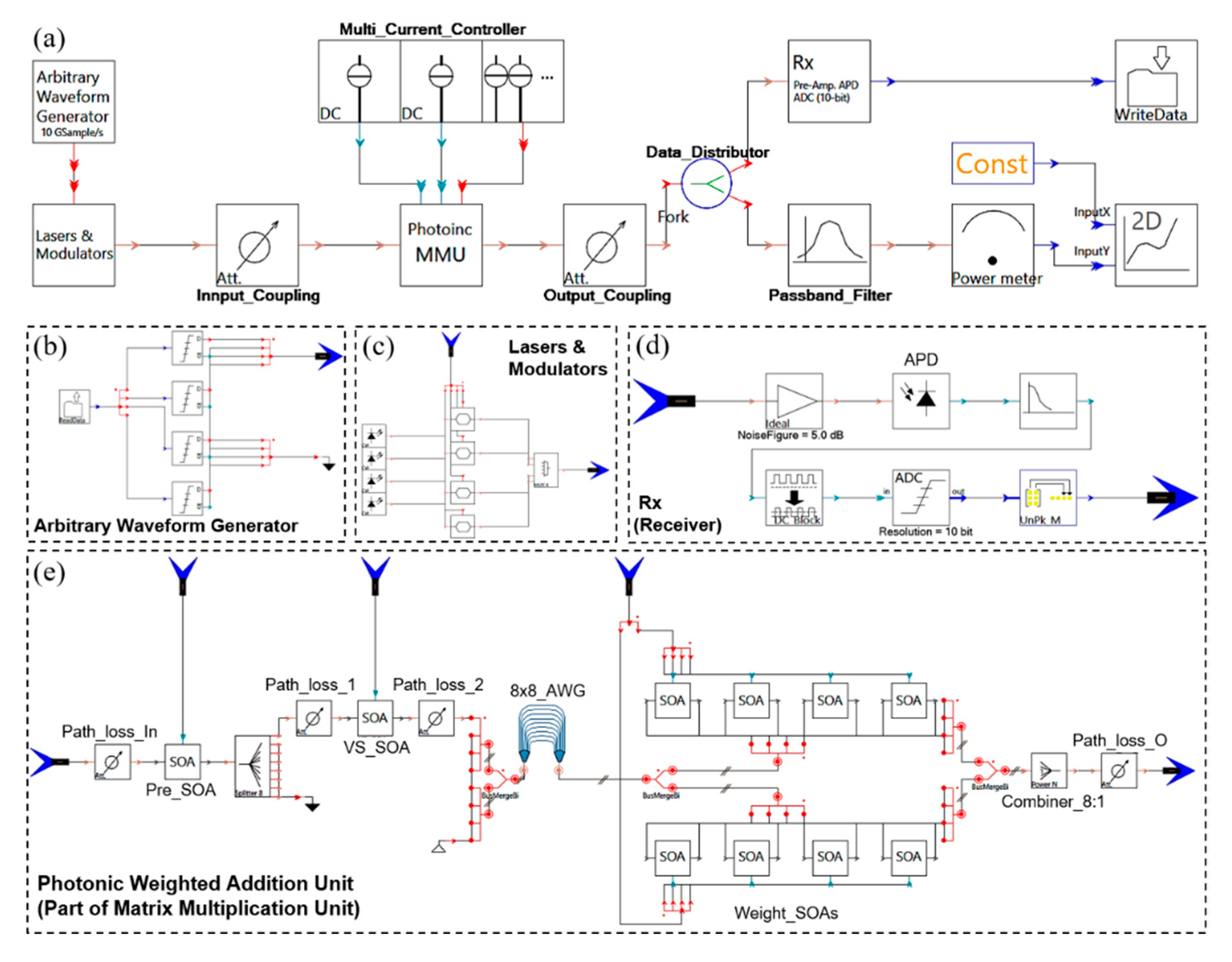
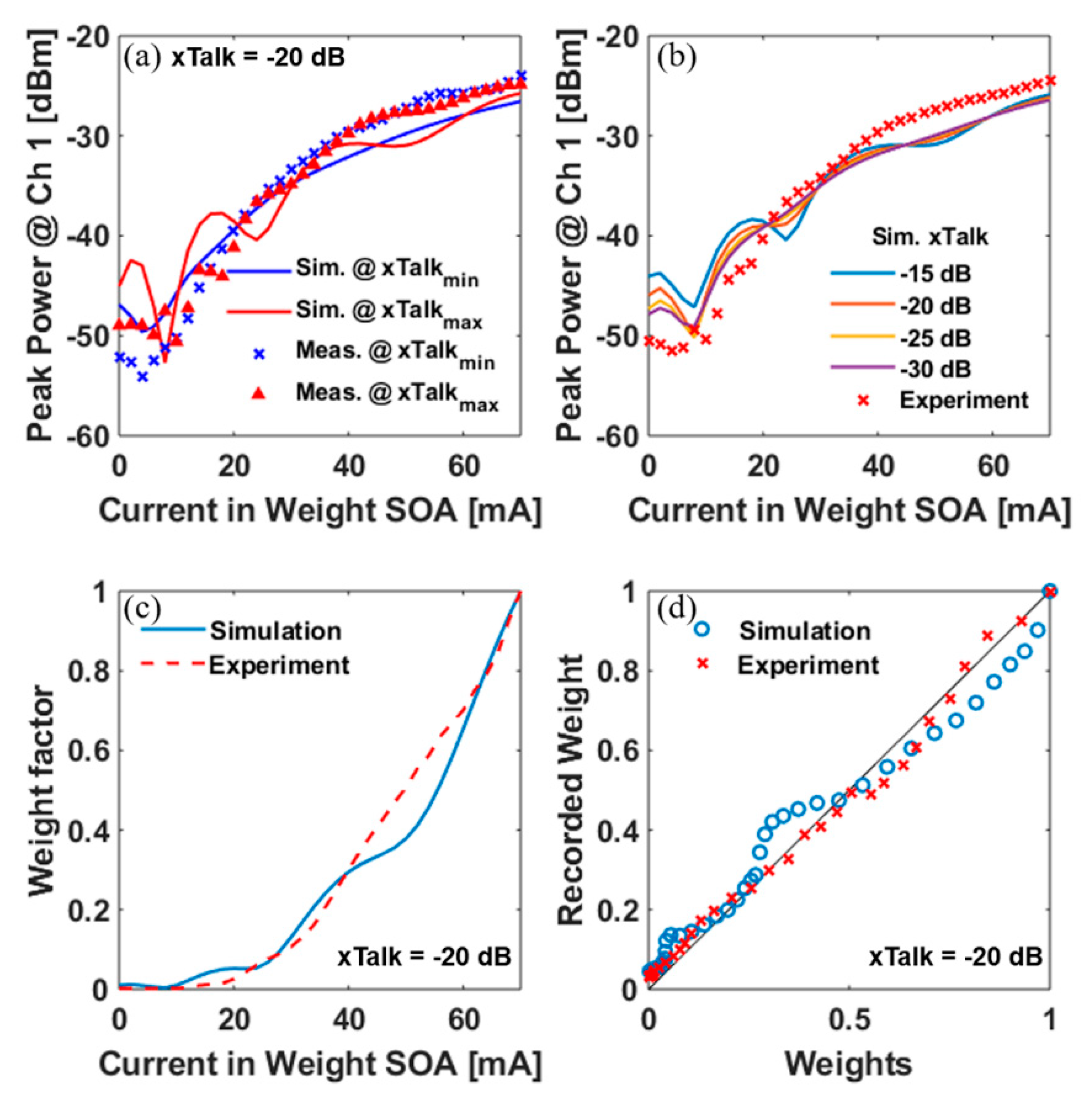
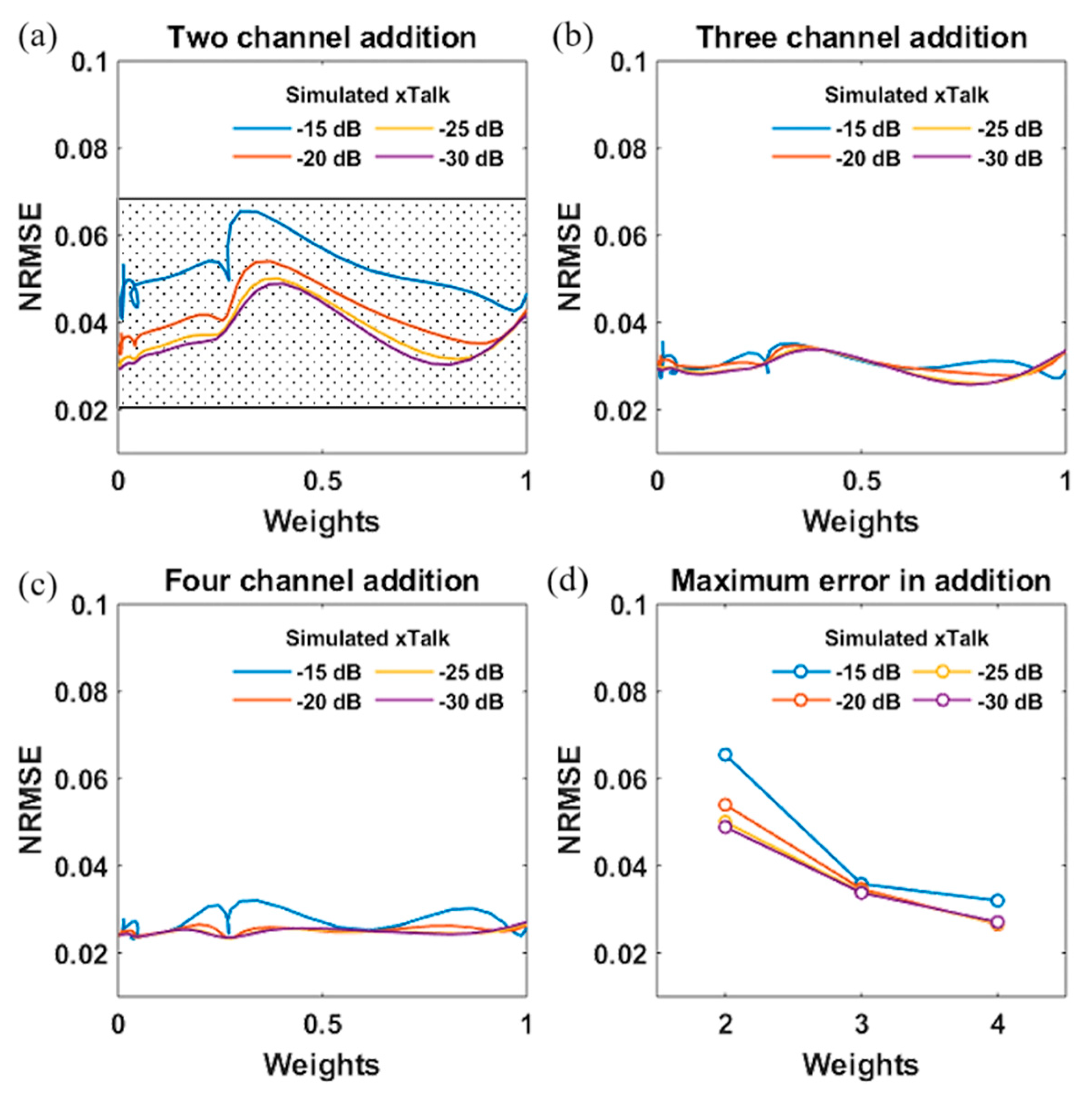
4. Implementation of Weight Calibration and Weighted Addition

For the operation of the SOA-based photonic neural network, a calibration of the weighting is required for correctly assigning the given weight factors to the input data. For this simulation implementation, the weight-SOAs are identical for all the input channels so that we demonstrate the weight calibration on one of the input channels. For the weight calibration, the input can be a non-return-to-zero on-off keying (NRZ OOK) signal or multi-level data input. As the weighting of the input data is performed after the AWG, the fixed optical crosstalk from the AWG will influence the output optical signal. We consider two extreme conditions for the optical crosstalk level: when switching ON (injection current at 70 mA) all the weight-SOAs, the optical crosstalk coming from the adjacent channels is expected to be maximum (XTalkmax), while when all the weight-SOAs are OFF (zero injected current), the induced optical crosstalk by that the corresponding channels will be the minimum (XTalkmin). Due to the complexity of operation conditions, we consider the average between these two scenarios in order to generate the weight control curve, in order to minimize the error induced by the optical interference.
The crosstalk in the AWG in the photonic MMU (see Figure 2e) is set at −20 dB, as experimentally measured in [33]. Firstly, when all the weight-SOAs are set to OFF (XTalkmin), but one of these weight-SOAs is injected with currents from 0 mA to 70 mA, we record the signal peak power at channel 1, 193.1 THz, from the monitoring power meter as shown in Figure 2a. Then, we also record the signal power when all the weight-SOAs are set to ON (XTalkmax), and one of these weight-SOAs is injected with currents from 0 mA to 70 mA. The blue and red solid lines in Figure 3a plot the simulated result in the condition of XTalkmin and XTalkmax, respectively. For comparison, we also superimpose the measured curves in both cases: the blue crosses curve represents the experiment points with all SOAs ON, and the red triangles curve plots the experimental results with all SOAs OFF.
The curve trends, in the case of simulation and experimental results, are very similar. We then scan the optical crosstalk level to investigate the influence of the optical crosstalk on the peak power curves. In Figure 3b, the blue, red, yellow and violet solid lines show the peak power on channel 1 (averaged from the curves shown in Figure 3a), where the simulated crosstalk for the AWG is set to −15 dB, −20 dB, −25 dB and −30 dB, respectively. It is visible that higher crosstalk will induce greater oscillation when tuning the injection current at the weight-SOA. The oscillation might be due to the interference between the crosstalk and the signal in the desired path. The experimental result is also presented with red crosses, which is the mean value of the experimental results shown in Figure 3a. The plots indicate that a dynamic range wider than 25 dB is possible. The slight difference between simulations and experiments may be attributed to the difference in gain efficiency as hypothesized for the SOA modeling. The weight control curve in Figure 3c is generated by the power control curves in Figure 3b, with reference weight ‘1’ level at −25 dBm optical input power, which is the signal peak power when injection current of the weight-SOA is set at 70 mA. The weight calibration curves show two semi-linear operation regimes, both for the simulation (Figure 3c, blue solid line) and the experiment (Figure 3c, red dashed line). These two regions correspond to the two different SOA operation regimes: the transparency operation and linear amplification. After the weight calibration, we obtain the correlation between the assigned weight and the obtained one for the simulated and the experimental operation in Figure 3d. An error lower than 0.12 for the simulation results is obtained, when compared to the reference perfect linear relation as shown by the black line.
The weighted addition corresponds to the linear operation part in a neuron. The performance of the weighted addition is of importance for the signal processing in a neural network. To estimate the impairments induced by the weighted addition, we calculate the normalized root mean square error (NRMSE), i.e., the discrepancy between the measured data and the expected data. We use the calibrated weight control curve to set the weight factors for different input channels, and calculate the NRMSE while tuning the weight factor from 0 to 1. Figure 4a plots the results of two-channel weighted addition, where channel 2 is fixed to the weight ‘1’, while the weight for channel 1 is tuned over the overall range from 0 to 1. We also change the optical crosstalk in the chip to see the impact of the optical crosstalk on the weighted addition. The blue, red, yellow and violet lines show the error changes when the crosstalk is set at −15 dB, −20 dB, −25 dB and −30 dB, respectively. The shaded area shows the error range obtained from the experiments for two-channel addition. The error variation is attributed to the calibration of the weight control, as already anticipated in the weight factor curve in Figure 3c. The error related to the weighted addition operation increases when the induced optical crosstalk is greater, as a high level of crosstalk eventually results in a lower dynamic range. The same high crosstalk level enhances the peak power oscillation recorded for generating the weight control curve, resulting in severe error variations, as already anticipated in Figure 3d. Nevertheless, this fits perfectly within the error variation window we found for our experimental results (see the dashed box in Figure 4a). The same analysis is done while changing the number of channels added to the WDM input. Figure 4b,c plot the resulting errors for three- and four-channel weighted additions, respectively. A visibly smaller error is presented for three-channel and four-channel weighted additions. The effect of the optical crosstalk is reduced as the oscillation power caused by the optical crosstalk is relatively smaller with respect to the dominating signal power coming from the addition of all the input multiple signals. This suggests that the higher the number of inputs into the neuron, the better the accuracy when operating within the available power budget. Finally, Figure 4d summarizes the obtained results, by plotting the maximum errors versus the number of channels in weighted addition.

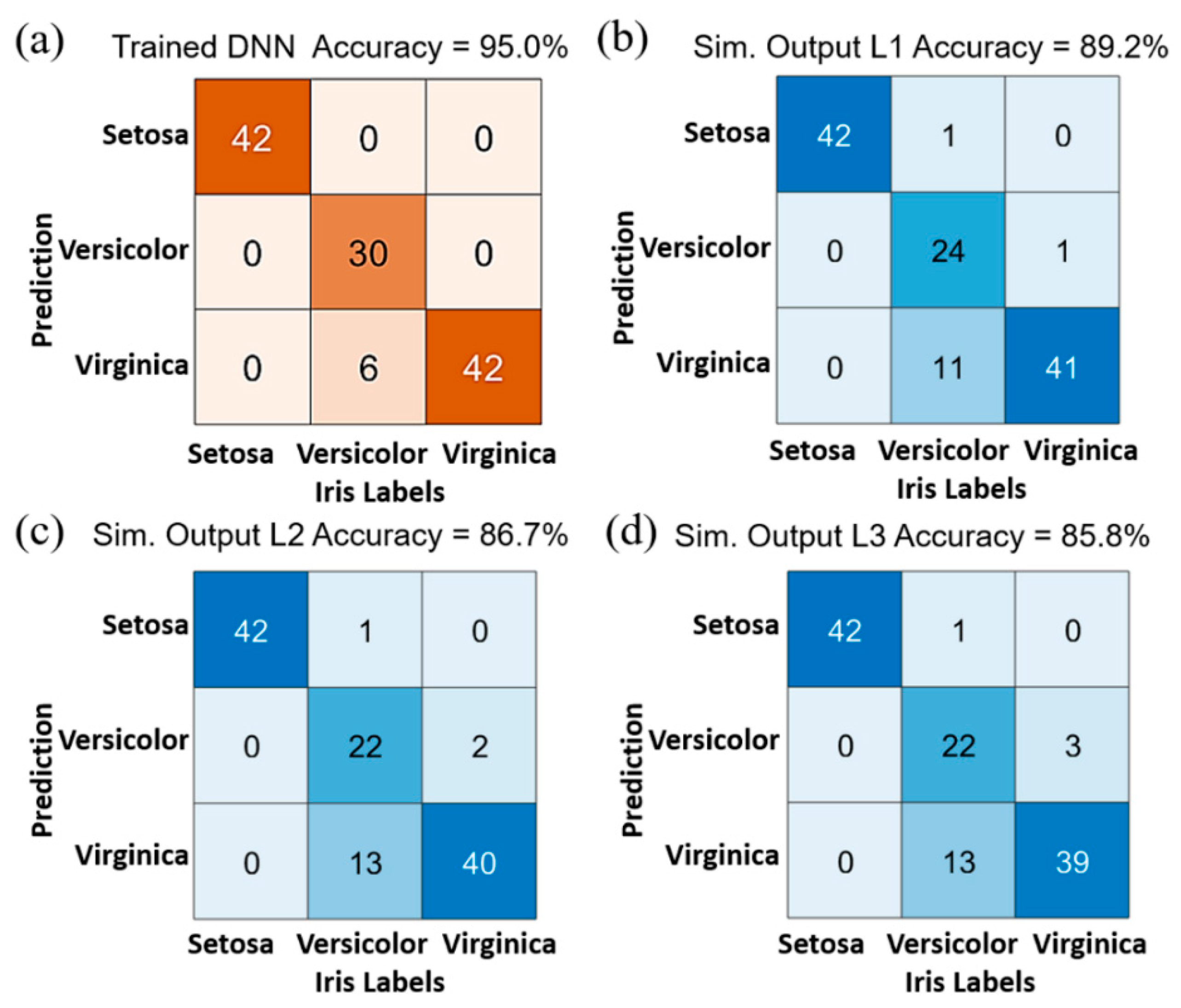
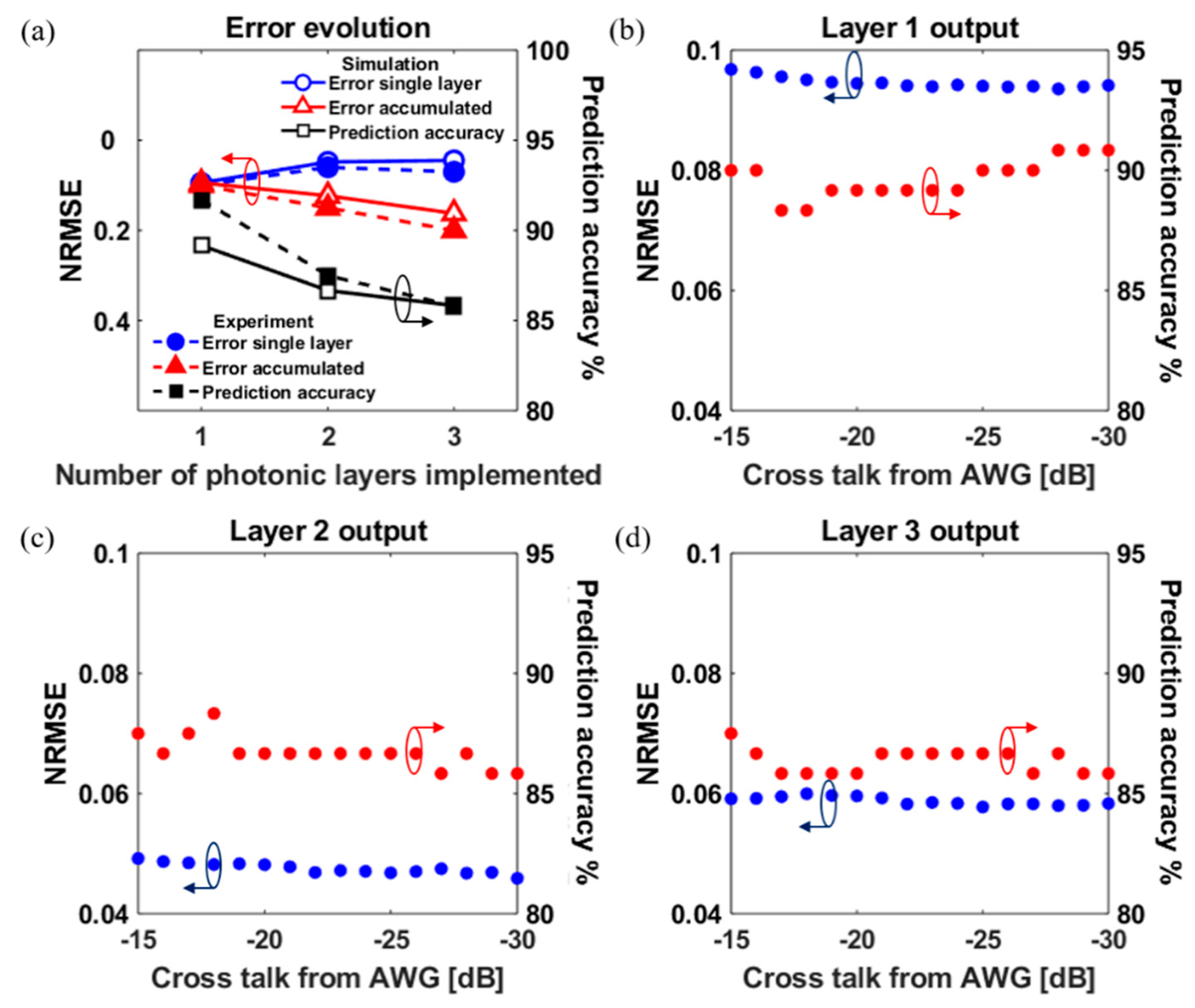
5. Image Classification via a Three-Layer Photonic Deep Neural Network

To investigate the performance of a complete neural network based on the combination of the AWG and SOA technology, for a broadcast-and-weight architecture, we implement and simulate an image classification problem, namely the iris flower classification problem, which has been reported to be able to be solved by using a deep neural network (DNN). The iris database includes three classes (Setosa, Versicolor, and Virginica) of 50 instances each [34]. Per each instance, the iris flower category is identified by observing four of its attributes: length and width of its sepals and petals. For this demonstration, we have executed the training of this DNN via the simulation platform Tensorflow [35], where we have used 120 instances as a training database. In order to make use of 4 weighted addition circuitries already available on chip and per layer, a feed-forward network made of 2 hidden layers with 4 neurons each and an output layer with 3 neurons (see Figure 5b), is trained on a computer. The attributes are encoded into 26 optical power levels at the photonic MMU input. The trained weight matrix is mapped to the matrix multiplication on the photonic components. The simulated structure of one layer of neurons is shown in Figure 5a, which is used to replace the photonic matrix multiplication unit in Figure 2e. The same chip is indeed capable of eight channel inputs, but we used four inputs for this classification problem. A total of 16 weight-SOAs in this matrix multiplication unit are used to assign the trained weight matrix from the trained DNN model to the PDNN. The hyperbolic tangent activation function is implemented offline after the O/E conversion. The output from the first hidden layer serves as input to the second layer (via the arbitrary waveform generator) and the output from the second hidden layer serves as input to the third (output) layer. Finally, the output of the third layer, after the SoftMax transfer function, P ( y = j ) = e y j / j = 1 n e y j , provides the predicted probability of the output samples y of belonging to class j. Figure 5c presents the output data at the output (i) of the 1st neuron in the 1st layer, (ii) of the 2nd layer and (iii) of the 3rd layer, with the blue line being the simulation results and red line the expectations and resulting in errors of 0.123, 0.051 and 0.055 respectively. These errors represent the performance of layers of photonic neurons. Higher error at the first layer may be due to the high optical signal noise ratio (OSNR) required multilevel encoding of the input signal, while a better performance at the 2nd and 3rd layer is attributed to the filtering of the signal level into lower levels after the first hidden layer. Also, the output of the first layer appears to be the most important for this classification problem, and therefore the utilization of three layers is slightly overstated.
The correlation matrix between the prediction and the labels of the samples is used to show the final accuracy obtained via the multilayer photonic neural network (see Figure 6). We consider three cases for the sake of understanding the influence of the photonic layer implementation. In Figure 6a we display the prediction accuracy as coming from the trained DNN on a PC. This is calculated to be 95% since 6 out of 120 iris flower instances are falsely predicted. We simulate the DNN after adding, time by time, the photonic deep neuron network layers. The prediction accuracy decreases as the number of layers of the photonic neural network increases. The accuracy changes from 89.7% when the 1st layer is substituted with a photonic layer (Figure 6b), down to 86.7% when both the 1st and the 2nd layers are substituted with photonic layers (Figure 6c), and down to 85.8% when all 3 layers of matrix multiplications are computed via three photonic layers (Figure 6d). This may be due to the error accumulation which causes prediction accuracy degradation. Furthermore, the simulation result aligns well with the experimental result trend as shown in Figure 7a.
Figure 7a plots the error evolution with an increasing number of the photonic layers. The solid lines with open symbols represent the results from the simulation and the dashed lines with filled symbols represent the experimental results. The circles show the error induced by each single layer on the 3-layer network, where the errors keep staying almost at the same level, about 0.07 in the simulation and 0.08 in the experiment. The triangles plot the accumulated error from layer to layer, which increases from 0.1 to 0.18 for simulation and from 0.10 to 0.20 in the experiment. The squares represent the final prediction accuracy as we calculated from the correlation matrix, which decreases from 89.2% to 85.8% as shown in Figure 6 for simulation and from 91.2% to 85.8% for experiments [27]. The experimental results show great agreement with the simulations, which means that investigating the performance while changing some of the parameters involved in the photonic integrated circuit (PIC) will help to get some insight into the photonic chip architecture and scalability. From the perspective of the final prediction accuracy and error induced by the photonic neural network chip, the impact of the optical crosstalk from the AWG and the waveguide crossings are investigated. We tune the crosstalk from −15 dB to −30 dB with 1 dB steps and implement the 3-layer neural network after generating the weight calibration curves as reported in Section 4. Figure 7b plots the results at the output of layer 1, with the blue line representing the average NRMSE from 4 neurons at layer 1 and the red line plotting the variation of the final prediction. Similarly, Figure 7c,d illustrate the average NRMSE and the final prediction versus the optical crosstalk in the layers. The error induced by the chip is almost in the same range for different crosstalk values, though it slightly reduces when the crosstalk decreases. The prediction accuracy for Layer 1 in Figure 7b shows a stronger crosstalk dependency; a smaller optical crosstalk at Layer 1 provides a better prediction accuracy. This may be related to the fact that the first layer operates on high resolution multilevel input signals, which require a higher optical to signal ratio available. A better accuracy also appears when the crosstalk is high, i.e., near −15 dB. This might be attributed to the errors leading the prediction of the flower label to a different minima location, i.e., to changes of the state of the network, as will also be found in Section 5. Figure 7c shows a flattened accuracy for optical crosstalk smaller than −20 dB. Figure 7d shows an even more flattened accuracy level as the variation of the induced error is smaller. The accuracy level is maintained from the 2nd layer onwards.

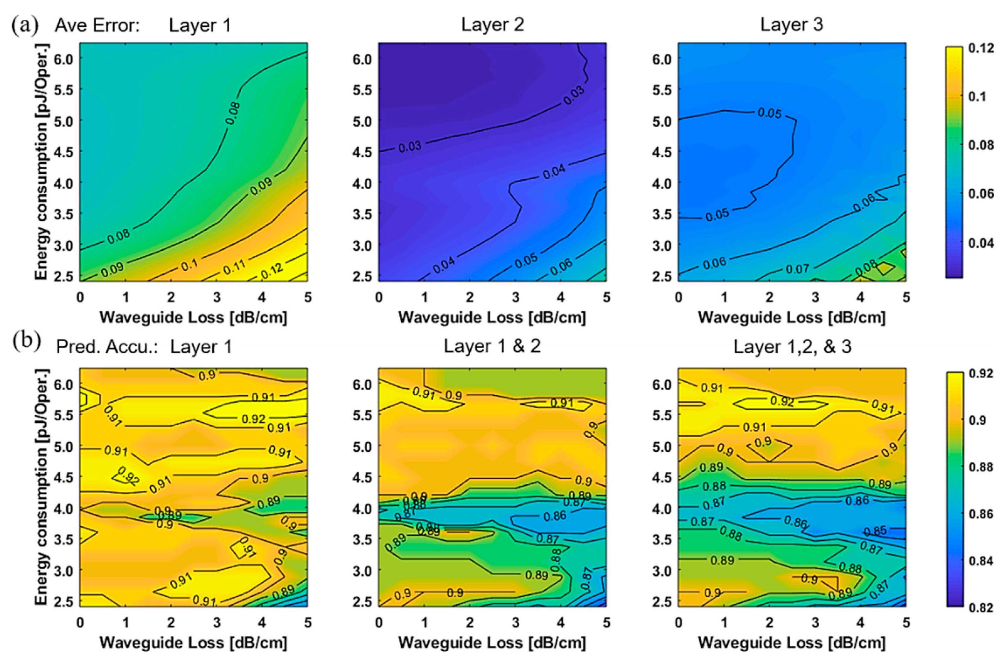
5.1. Energy Consumption Versus Physical Layer Impairments

The performance of the PDNN is expected to be influenced also by the reference energy level used to operate the optical engine and by the loss on chip. Therefore, we study the performances of the PDNN by executing the iris classification problem, while tuning the reference power level of weight factor ‘1’ used in the integrated circuit, i.e., while tuning the current used in the SOAs, as well as while assuming different waveguide losses for the optical paths. This analysis is carried out to understand opportunities for energy savings and best chip physical layer characteristics, which still guarantee a high level of prediction accuracy. In particular, for this analysis, we consider only the waveguide loss as the main loss component as this is true for large size PIC. Therefore, we calculate the NRMSE at the output of each photonic neuron layer, as well as the prediction accuracy obtained when involving this layer in the 3-layer DNN for the iris flower classification, and we provide 3D color maps of error and accuracy as a function of the scanning waveguide losses and energy consumption on different reference power levels. Figure 8a illustrates the average errors obtained at the output of the 1st layer, the 2nd layer and the 3rd layer as a function of the waveguide loss and the energy consumption. It can be observed that fewer losses allow less energy consumption, for the same error level. This suggests that by only improving the waveguide loss on chip we can double the energy savings. The induced error from the photonic DNN is expected to be greater when the waveguide losses are higher and the energy consumption per operation at the matrix multiplication unit is lower, as the dynamic range is not enough to be able to distinguish multilevel data. On the contrary, smaller error values are observed with lower waveguide loss and higher energy used for the weighted addition operations (see moving from lighter color to darker color, from bottom right to top left side in Figure 8a and for each layer). For Layer 1 this is more evident and is coherent with our previous conclusions. It is not surprising that we need to either tune the reference power to higher levels or reduce the waveguide loss to obtain smaller errors at the neuron signal processing.
Furthermore, the final prediction accuracies for the cases when Layer 1, Layers 1 and 2, and all three layers are implemented by using the photonic integrated chip are shown in Figure 8b. The yellow color corresponds to a higher prediction accuracy, while the blue color corresponds to a lower prediction accuracy. The prediction accuracy results do not show the same trend as shown in Figure 8a, i.e., the trend for the error induced on the layer operations, which indicates that an induced error is not necessarily reducing the performance of the photonic neural network. The result for Layer 1 shows that a good prediction is obtained for an error smaller than 0.09 and in that region the accuracy remains generally very stable, while the accuracy for higher error levels is variable, and generally worse. This suggests that there is a certain maximum level of error we should never cross at the first layer for always guaranteeing a good accuracy. The prediction mapping from the implementation of Layers 1 and 2 shows a slight decrease in the accuracy as the error accumulated from the previous layer. In the case of adding the contribution of Layer 3, it is the result of the small error accumulation as well, for the final prediction accuracy on this 3-layer photonic neural network system. However, it is evident that the two different regions are delineated when more error is accumulated from layer to layer. In particular, for the complete 3-layer photonic neural network, the best performance condition (accuracy = 92%) is found when the energy efficiency is around 5.6 pJ/operation and the waveguide loss ranges between 1.5 and 3.5 dB/cm. However it is possible to distinguish two areas where the accuracy is already higher than 89%: (1) the total energy consumption is above 4.5 pJ/operation, irrespective of the path loss; (2) the area at the left down corner where the averaged energy consumption is around 2.8 pJ/operation and the loss covers almost the full considered range (up to 4 dB/cm). The region (1) performs well due to a higher signal power with higher power consumption on the system with smaller errors induced and accumulated. We believe the region (2) appears due to the presence of more local minima, whose presence is determined by the combination of path losses, power level and optical crosstalk. Furthermore, the level of noise present in the network makes it a stochastic network where the intrinsic noise is supposed to provide better accuracy. Noise might play a positive role for low power levels as a good prediction is presented. However, this behavior has to be further explored for quantification. The identification of small error regions and their slight influence on the final prediction accuracy, as well as the maximum level of error at the first layer shown in Figure 8 suggests that the PDNN might be further scaled up, with prior physical parameters and error optimization.

6. Conclusions

We propose a photonic deep neural network based on the use of WDM input signals, and an SOA-based matrix multiplication unit. The integrated photonic neural network is employed as a weighted addition, thereafter combined with an offline hyperbolic tangent function as a nonlinear function is demonstrated on the simulation platform VPIphotonics. We study the weight calibration and weighted addition with different crosstalk of photonic integrated AWGs and SOA-based cross-connects. The error from the weighted addition is found to decrease when the numbers of input channels increase, so that a high number of input channels is beneficial for the implementation of the PDNN. A trained 3-layer DNN is implemented by reconfiguring the weight setting on the subnetwork and feeding the layer output to the next layer. The performance is simulated with different values of crosstalk, energy consumption per operation, and waveguide loss. The experimental results are in agreement with the simulation results, meaning that the implemented simulation offers a solid base for further study of scalability for this kind of network architecture. The results show that the photonic DNN is robust to the noise added during the signal processing. The error induced by the first layer is greater than the next two layers, due to the higher resolution multilevel encoding at the input layer with respect to the resolution at the 2nd and 3rd layer, but the error is not necessarily degrading the performance for a maximum allowed error. The performance analysis as a function of the path losses suggests the photonic neural network could be further optimized for lower power consumption. These results provide enough insights for the design of scalable photonic neural networks to a higher dimension for solving higher complexity problems. Finally, in future, a combination of the weighted addition function with on-chip non-linearities holds the promise to enable further acceleration for computation.

Author Contributions

Conceptualization, B.S., N.C. and R.S.; formal analysis, B.S. and R.S.; investigation, B.S.; methodology, B.S., N.C. and R.S.; validation, B.S.; visualization, B.S.; writing—review & editing, B.S., N.C. and R.S. All authors have read and agreed to the published version of the manuscript.

Funding

This work is financially supported by the Netherlands Organization of Scientific Research (NWO) under the Gravitation program (Zwaartekracht programma), ‘Research Centre for Integrated Nanophotonics’.

Acknowledgments

The authors thank the technical support from VPIphotonics.

Conflicts of Interest

The authors declare no conflict of interest.

References

  1. McAfee, A.; Brynjolfsson, E. Big Data: the Management Revolution. Harv. Bus. Rev. 2012, 90, 60–66, 68, 128. [Google Scholar] [PubMed]
  2. Philip Chen, C.L.; Zhang, C.-Y. Data-Intensive Applications, Challenges, Techniques and Technologies: A Survey on Big Data. Inf. Sci. (Ny) 2014, 275, 314–347. [Google Scholar] [CrossRef]
  3. Masci, J.; Meier, U.; Cire, D. Stacked Convolutional Auto-Encoders for Hierarchical Feature Extraction. In Proceedings of the Artificial Neural Networks and Machine Learning-ICANN 2011; Honkela, T., Duch, W., Girolami, M., Kaski, S., Eds.; Springer: Berlin, Germany, 2011; pp. 52–59. [Google Scholar]
  4. Lawrence, S.; Giles, C.L.; Tsoi, A.C.; Back, A.D. Face Recognition: A Convolutional Neural-Network Approach. IEEE Trans. Neural Netw. 1997, 8, 98–113. [Google Scholar] [CrossRef] [Green Version]
  5. Hill, T.; O’Connor, M.; Remus, W. Neural Network Models for Time Series Forecasts. Manag. Sci. 1996, 42, 1082–1092. [Google Scholar] [CrossRef]
  6. Chow, T.T.; Zhang, G.Q.; Lin, Z.; Song, C.L. Global Optimization of Absorption Chiller System by Genetic Algorithm and Neural Network. Energy Build. 2002, 34, 103–109. [Google Scholar] [CrossRef]
  7. Zeng, H.; Edwards, M.D.; Liu, G.; Gifford, D.K. Convolutional Neural Network Architectures for Predicting DNA–Protein Binding. Bioinformatics 2016, 32, i121–i127. [Google Scholar] [CrossRef]
  8. Ball, N.M.; Brunner, R.J. Data Mining and Machine Learning in Astronomy. Int. J. Mod. Phys. D 2010, 19, 1049–1106. [Google Scholar] [CrossRef] [Green Version]
  9. Cannas, B.; Fanni, A.; Marongiu, E.; Sonato, P. Disruption Forecasting at JET Using Neural Networks. Nucl. Fusion 2004, 44, 68–76. [Google Scholar] [CrossRef]
  10. Fischer, M.M.; Gopal, S. Artificial Neural Networks: A New Approach to Modeling Interregional Telecommunication Flows. J. Reg. Sci. 1994, 34, 503–527. [Google Scholar]
  11. Akopyan, F.; Sawada, J.; Cassidy, A.; Alvarez-Icaza, R.; Arthur, J.; Merolla, P.; Imam, N.; Nakamura, Y.; Datta, P.; Nam, G.J.; et al. TrueNorth: Design and Tool Flow of a 65 mW 1 Million Neuron Programmable Neurosynaptic Chip. IEEE Trans. Comput. Des. Integr. Circuits Syst. 2015, 34, 1537–1557. [Google Scholar] [CrossRef]
  12. Benjamin, B.V.; Gao, P.; McQuinn, E.; Choudhary, S.; Chandrasekaran, A.R.; Bussat, J.; Alvarez-Icaza, R.; Arthur, J.V.; Merolla, P.A.; Boahen, K. Neurogrid: A Mixed-Analog-Digital Multichip System for Large-Scale Neural Simulations. Proc. IEEE 2014, 102, 699–716. [Google Scholar] [CrossRef]
  13. Furber, S.B.; Galluppi, F.; Temple, S.; Plana, L.A. The SpiNNaker Project. Proc. IEEE 2014, 102, 652–665. [Google Scholar] [CrossRef]
  14. Neckar, A.; Fok, S.; Benjamin, B.V.; Stewart, T.C.; Oza, N.N.; Voelker, A.R.; Eliasmith, C.; Manohar, R.; Boahen, K. Braindrop: A Mixed-Signal Neuromorphic Architecture with a Dynamical Systems-Based Programming Model. Proc. IEEE 2019, 107, 144–164. [Google Scholar] [CrossRef]
  15. Zhang, C.; Li, P.; Sun, G.; Guan, Y.; Xiao, B.; Cong, J. Optimizing FPGA-Based Accelerator Design for Deep Convolutional Neural Networks. In Proceedings of the FPGA 2015–2015 ACM/SIGDA International Symposium on Field-Programmable Gate Arrays, Monterey, CA, USA, 22–24 February 2015; ACM Press: New York, NY, USA, 2015; pp. 161–170. [Google Scholar]
  16. Han, S.; Liu, X.; Mao, H.; Pu, J.; Pedram, A.; Horowitz, M.A.; Dally, W.J. EIE: Efficient Inference Engine on Compressed Deep Neural Network. In Proceedings of the 2016 ACM/IEEE 43rd Annual International Symposium on Computer Architecture (ISCA), Seoul, Korea, 18–22 June 2016; pp. 243–254. [Google Scholar]
  17. Jouppi, N.P.; Borchers, A.; Boyle, R.; Cantin, P.; Chao, C.; Clark, C.; Coriell, J.; Daley, M.; Dau, M.; Dean, J.; et al. In-Datacenter Performance Analysis of a Tensor Processing Unit. In Proceedings of the Proceedings-International Symposium on Computer Architecture, Toronto, ON, Canada, 24–28 June 2017; ACM Press: New York, NY, USA, 2017; pp. 1–12. [Google Scholar]
  18. Kravtsov, K.S.; Fok, M.P.; Prucnal, P.R.; Rosenbluth, D. Ultrafast All-Optical Implementation of a Leaky Integrate-and-Fire Neuron. Opt. Express 2011, 19, 2133–2147. [Google Scholar] [CrossRef]
  19. Bueno, J.; Maktoobi, S.; Froehly, L.; Fischer, I.; Jacquot, M.; Larger, L.; Brunner, D. Reinforcement Learning in a Large-Scale Photonic Recurrent Neural Network. Optica 2018, 5, 756–760. [Google Scholar] [CrossRef] [Green Version]
  20. Nakayama, J.; Kanno, K.; Uchida, A. Laser Dynamical Reservoir Computing with Consistency: An Approach of a Chaos Mask Signal. Opt. Express 2016, 24, 8679–8692. [Google Scholar] [CrossRef]
  21. Stabile, R.; Rohit, A.; Williams, K.A. Monolithically Integrated 8 × 8 Space and Wavelength Selective Cross-Connect. J. Light. Technol. 2014, 32, 201–207. [Google Scholar] [CrossRef]
  22. Smit, M.; Leijtens, X.; Ambrosius, H.; Bente, E.; van der Tol, J.; Smalbrugge, B.; de Vries, T.; Geluk, E.-J.; Bolk, J.; van Veldhoven, R.; et al. An Introduction to InP-Based Generic Integration Technology. Semicond. Sci. Technol. 2014, 29, 083001. [Google Scholar] [CrossRef]
  23. Vandoorne, K.; Dambre, J.; Verstraeten, D.; Schrauwen, B.; Bienstman, P. Parallel Reservoir Computing Using Optical Amplifiers. IEEE Trans. Neural Netw. 2011, 22, 1469–1481. [Google Scholar] [CrossRef]
  24. Vandoorne, K.; Mechet, P.; Van Vaerenbergh, T.; Fiers, M.; Morthier, G.; Verstraeten, D.; Schrauwen, B.; Dambre, J.; Bienstman, P. Experimental Demonstration of Reservoir Computing on a Silicon Photonics Chip. Nat. Commun. 2014, 5, 3541. [Google Scholar] [CrossRef] [Green Version]
  25. Shen, Y.; Harris, N.C.; Skirlo, S.; Prabhu, M.; Baehr-Jones, T.; Hochberg, M.; Sun, X.; Zhao, S.; Larochelle, H.; Englund, D.; et al. Deep Learning with Coherent Nanophotonic Circuits. Nat. Photonics 2017, 11, 441–446. [Google Scholar] [CrossRef]
  26. Tait, A.N.; De Lima, T.F.; Zhou, E.; Wu, A.X.; Nahmias, M.A.; Shastri, B.J.; Prucnal, P.R. Neuromorphic Photonic Networks Using Silicon Photonic Weight Banks. Sci. Rep. 2017, 7, 1–10. [Google Scholar] [CrossRef] [PubMed]
  27. Shi, B.; Calabretta, N.; Stabile, R. Deep Neural Network Through an InP SOA-Based Photonic Integrated Cross-Connect. IEEE J. Sel. Top. Quantum Electron. 2020, 26, 1–11. [Google Scholar] [CrossRef]
  28. Peng, H.-T.; Nahmias, M.A.; de Lima, T.F.; Tait, A.N.; Shastri, B.J. Neuromorphic Photonic Integrated Circuits. IEEE J. Sel. Top. Quantum Electron. 2018, 24, 1–15. [Google Scholar] [CrossRef]
  29. Nahmias, M.A.; Peng, H.-T.; de Lima, T.F.; Huang, C.; Tait, A.N.; Shastri, B.J.; Prucnal, P.R. A TeraMAC Neuromorphic Photonic Processor. In Proceedings of the 2018 IEEE Photonics Conference (IPC), Reston, VA, USA, 30 September–4 October 2018; pp. 1–2. [Google Scholar]
  30. Mourgias-Alexandris, G.; Tsakyridis, A.; Passalis, N.; Tefas, A.; Vyrsokinos, K.; Pleros, N. An all-Optical Neuron with Sigmoid Activation Function. Opt. Express 2019, 27, 9620. [Google Scholar] [CrossRef]
  31. LeCun, Y.; Bottou, L.; Bengio, Y.; Haffner, P. Gradient-Based Learning Applied to Document Recognition. Proc. IEEE 1998, 86, 2278–2323. [Google Scholar] [CrossRef] [Green Version]
  32. Lowery, A.J. Amplified Spontaneous Emission in Semiconductor Laser Amplifiers. Validity of the Transmission-Line Laser Model. IEE Proc. Part J. Optoelectron. 1990, 137, 241–247. [Google Scholar] [CrossRef]
  33. Stabile, R.; Rohit, A.; Williams, K.A. Dynamic Multi-Path WDM Routing in a Monolithically Integrated 8 × 8 Cross-Connect. Opt. Express 2014, 22, 435–442. [Google Scholar] [CrossRef] [Green Version]
  34. Fisher, R.A. The Use of Multipe Measurements in Taxonomic Problems. Ann. Eugen. 1936, 7, 179–188. [Google Scholar] [CrossRef]
  35. Chan, T.-H.; Jia, K.; Gao, S.; Lu, J.; Zeng, Z.; Ma, Y. PCANet: A Simple Deep Learning Baseline for Image Classification? IEEE Trans. Image Process. 2015, 24, 5017–5032. [Google Scholar] [CrossRef] [Green Version]
Figure 1. Photonic deep neural network based on the broadcast-and-weight architecture. (a) The artificial neuron model. (b) The implementation via arrays of semiconductor optical amplifiers (SOAs). (c) One full layer of neurons by exploiting one wavelength division multiplexing (WDM) input, with a shaded photonic integrated circuit micrography at the back, to underline that part of the circuitry that is realized on chip. (d) Scheme of a three-layer photonic deep neural network. The included port selector may be used to select the desired input source.
Applsci 10 00474 g001
Figure 2. Photonic deep neural network (PDNN) simulation scheme on software VPIphotonics. (a) System for examining the PDNN. (b) Arbitrary waveform generator. (c) Lasers and modulators. (d) Receiver. (e) One photonic weighted addition unit (part of the matrix multiplication unit, MMU).
Applsci 10 00474 g002
Figure 3. Weight calibration. (a) Peak power of channel at 193.1 THz with minimum crosstalk (blue) and maximum crosstalk (red), in simulation (solid line), or experiment (cross/triangle points), versus the injection current at the weight-SOA. (b) Mean peak power of channel at 193.1 THz from the two curves obtained in (a), and with simulated crosstalk at −15 dB, −20 dB, −25 dB and −30 dB. (c) Weight control curves, in simulation (solid line) and experiment (dash line), with crosstalk of −20 dB and reference power level at −25 dBm. (d) Correlation between the weight assigned by the weight-SOA and the obtained weight at the output, in simulation (blue circles) and experiments (red crosses). The black line is a reference line for perfect matching.
Applsci 10 00474 g003
Figure 4. (a) Two-channel weighted addition, (b) three-channel addition, and (c) four-channel addition when tuning weights in channel 1 and fixed weight on other channels; (d) Maximum error versus the number of channels in weighted addition. Optical crosstalk levels are −15 dB (blue), −20 dB (red), −25 dB (yellow) and −30 dB (violet).
Applsci 10 00474 g004
Figure 5. (a) The simulation structure of one layer of neurons; (b) Trained 3-layer deep neural network (DNN) employed to solve the iris flower classification. (c) Output data obtained from Neuron 1 at (i) Layer 1, (ii) Layer 2, and (iii) Layer 3, with calculated errors between simulated computation (blue line) and the expected computation (red line), resulting in errors of 0.123, 0.051, and 0.055, respectively.
Applsci 10 00474 g005
Figure 6. (a) Label prediction of the trained DNN, indicating an accuracy of 95%. (b) Simulated image prediction using photonic DNN as the 1st hidden layer, with an accuracy of 89.2%. (c) Simulated label prediction using photonic DNN as the 1st and 2nd hidden layers, with an accuracy of 86.7%. (d) Simulated label prediction of the 3-layer photonic DNN, with an accuracy of 85.8%.
Applsci 10 00474 g006
Figure 7. Error evolution: (a) Normalized root mean square error (NRMSE) versus the number of implemented photonic layers in simulation (solid line filled points) and experiment (dashed line open points), from single photonic layer (circles), the accumulation (triangles) and the corresponding prediction accuracy (squares). Crosstalk tuning: The induced error (blue circles) and the final prediction accuracy (red circles) versus the crosstalk from AWGs, recorded simulation results from (b) output of layer 1, (c) output of layer 2, and (d) output of layer 3.
Applsci 10 00474 g007
Figure 8. Investigation performance of the PDNN on computing energy and waveguide loss. (a) Calculated average NRMSE from output data obtained from Layers 1–3; (b) Corresponding prediction accuracy when Layer 1, Layers 1,2, and Layers 1–3 are implemented with photonic neuron layers.
Applsci 10 00474 g008
Table 1. The parameters used in the simulation of SOA.
ParametersValueUnitParametersValueUnit
Device Section Length1000 × 10−6mNonlinear Gain Coefficient1.0 × 10−23m3
Active Region TypeMQW Nonlinear Gain Time Constant5.00 × 10−13s
Active Region Width2.0 × 10−6mCarrier Density Transparency1.0 × 1024m−3
Active Region Thickness250 × 10−6mLinear Recombination1.0 × 108s−1
Active Region Thickness MQW100 × 10−6mBimolecular Recombination1.0 × 10−16m3/s
Active Region Thickness SCH200 × 10−6mAuger Recombination2.1 × 10−41m6/s
Current Injection Efficiency1 Carrier Capture Time Constant3.0 × 10−11s
Nominal Frequency193.7THzCarrier Escape Time Constant1.0 × 10−10s
Group Index3.52 Initial Carrier Density8.0 × 1023m−3
Polarization ModelTE Chirp ModelLinewidth Factor
Internal Loss3000m−1Linewidth Factor3
Confinement Factor0.3 Linewidth Factor MQW3
Confinement Factor MQW0.07 Differential Index−1.0 × 10⁻²⁶m3
Confinement Factor SCH0.56 Differential Index MQW−1.0 × 10⁻²⁶m3
Gain Shape ModelFlat Differential Index SCH−1.5 × 10⁻²⁶m3
Gain ModelLogarithmicCarrier Density Ref. Index1.0 × 1024m−3
Gain Coefficient Linear4.00 × 10−20m2Noise ModelInversion Parameter
Gain Coefficient Logarithmic6.9 × 104m−1Inversion Parameter1.2

