Review

Silicon Integrated Nanophotonic Devices for On-Chip Multi-Mode Interconnects

State Key Laboratory for Modern Optical Instrumentation, Center for Optical & Electromagnetic Research, College of Optical Science and Engineering, International Research Center for Advanced Photonics, Zijingang Campus, Zhejiang University, Hangzhou 310058, China
*
Author to whom correspondence should be addressed.
Appl. Sci. 2020, 10(18), 6365; https://doi.org/10.3390/app10186365
Submission received: 17 August 2020 / Revised: 9 September 2020 / Accepted: 11 September 2020 / Published: 12 September 2020

Abstract

:
Mode-division multiplexing (MDM) technology has drawn tremendous attention for its ability to expand the link capacity within a single-wavelength carrier, paving the way for large-scale on-chip data communications. In the MDM system, the signals are carried by a series of higher-order modes in a multi-mode bus waveguide. Hence, it is essential to develop on-chip mode-handling devices. Silicon-on-insulator (SOI) has been considered as a promising platform to realize MDM since it provides an ultra-high-index contrast and mature fabrication processes. In this paper, we review the recent progresses on silicon integrated nanophotonic devices for MDM applications. We firstly discuss the working principles and device configurations of mode (de)multiplexers. In the second section, we summarize the multi-mode routing devices, including multi-mode bends, multi-mode crossings and multi-mode splitters. The inverse-designed multi-mode devices are then discussed in the third section. We also provide a discussion about the emerging reconfigurable MDM devices in the fourth section. Finally, we offer our outlook of the development prospects for on-chip multi-mode photonics.

1. Introduction

The modern micro-processors require an extremely large link capacity for data communications between multi-cores and local/distant caches [1]. However, it is becoming increasingly difficult to meet the ever-growing capacity requirement since the conventional electrical interconnects severely suffer from limited bandwidth and significant power consumption [2]. The on-chip optical-interconnect technology emerges as an attractive approach to break the bottleneck [2,3,4], taking advantage of its ultra-large bandwidth and ultra-low power consumption. Moreover, the link capacity can be further enhanced for the optical interconnects by utilizing novel multiplexing technologies, including wavelength-division multiplexing (WDM) [5,6,7,8,9], polarization-division multiplexing (PDM) [10] and mode-division multiplexing (MDM) [11,12,13]. WDM technology has been widely used in optical communication systems. For WDM, different signals are carried by different wavelengths, so WDMs always require a large number of laser diodes (LDs) each with an accurate temperature monitor, leading to complicated and expensive systems [11]. Therefore, it is necessary to expand the link capacity within a single-wavelength carrier by utilizing the cost-effective PDM and MDM technologies. Note that polarizations can only contribute two degrees of freedom, i.e., transverse electric (TE) and transverse magnetic (TM), so the PDM technology can only double the link capacity [10]. In contrast, the MDM system is much more scalable since the total mode capacity can be easily expanded by choosing a relatively wide multi-mode bus waveguide, showing enormous potential for achieving large-scale on-chip optical interconnects with great scalability.
In recent years, silicon-on-insulator (SOI) has been regarded as a promising platform to develop multi-mode photonics for its ultra-high-index contrast (nSi ≈ 3.46, nSiO2 ≈ 1.45) and mature fabrication processes compatible with complementary metal oxide semiconductors (CMOS) [14,15,16,17,18,19,20,21,22]. Figure 1a shows the calculated effective indices for the higher-order modes in a SOI waveguide with varied core width (wwg). Here, the waveguide thickness is chosen to be hwg = 220 nm and the cladding material is chosen to be SiO2. Figure 1b shows the calculated mode profiles for the first four TE/TM modes with wwg = 2 μm. From Figure 1a,b, one can observe the strong waveguide birefringence and mode dispersion, which makes it possible to realize selective mode handling without introducing much inter-modal crosstalk. Figure 1c shows the configuration for a typical MDM system (four channels with TE0–3 modes are considered here as an example). The fundamental TE mode (i.e., TE0) from a single LD is firstly divided to four waveguide channels by power splitters. The waveguide channels are then independently modulated and converted/multiplexed to the higher-order modes (i.e., TE0–3) in the multi-mode bus waveguide by using the mode multiplexer. At the receiver terminal, TE0–3 modes are reverted to TE0 mode in different waveguide channels by the mode demultiplexer and received by the photodetectors (PDs). It can be seen from the configuration that the higher-order modes only exist in the multi-mode bus waveguide, while the other components (e.g., LDs, modulators and PDs) all work under the fundamental mode. Therefore, the basic MDM components could be classified into two categories:
  • The mode (de)multiplexers for interfacing single-mode input/output waveguides and multi-mode bus waveguide.
  • The multi-mode routing devices (e.g., bend, crossing and splitter) for transferring higher-order modes in the multi-mode bus waveguide.
Complex MDM systems can be built by simply combining these two kinds of basic MDM components with other conventional single-mode components.
In this paper, we review the recent progress on silicon integrated nanophotonic devices for on-chip multi-mode interconnects. In Section 2, we begin by reviewing silicon multi-dimensional (de)multiplexers, including silicon mode multiplexers in Section 2.1, silicon hybrid multiplexers in Section 2.2, and densely packed waveguide arrays in Section 2.3. In Section 3, we give a review on silicon multi-mode routing devices, including silicon multi-mode bends in Section 3.1, silicon multi-mode crossings in Section 3.2, and silicon multi-mode splitters in Section 3.3. In Section 4, we turn to the discussion of inverse-designed multi-mode devices. In Section 5, we give a review on reconfigurable MDM devices. In Section 6, we offer our outlook of the development prospects for silicon multi-mode photonics. Figure 2 illustrates the main topics that will be discussed in the following sections.

2. Silicon Multi-Dimensional (De)Multiplexers

The mode (de)multiplexer is one of the most important elements in the MDM system, which is used to realize mode conversion and combine/separate signals carried by different modes. Over the recent years, various mode (de)multiplexers have been proposed and demonstrated on the SOI platform, which will be reviewed in Section 2.1. The link capacity can be further enhanced for multi-mode data communications by introducing some other dimensions, such as wavelengths and polarizations. The hybrid (de)multiplexer enables the simultaneous combination/separation of signals carried by multiple degrees of freedom, which is crucial in WDM/PDM/MDM hybrid systems. A review on silicon hybrid (de)multiplexers will be given in Section 2.2. The mode capacity can also be improved by employing spatially separated super-modes in the densely packed waveguide array (DPWA). Silicon–DPWA-based mode (de)multiplexers will be reviewed in Section 2.3.

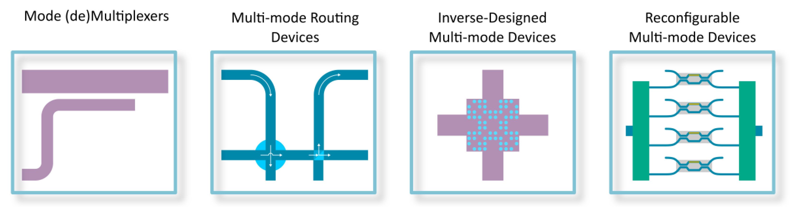
2.1. Silicon Mode (De)Multiplexers

The mode (de)multiplexer enables mode conversion and signal (de)multiplexing. Such functionalities can be achieved by various different structures, e.g., multimode interference couplers (MMIs) [23,24,25,26,27,28], asymmetric Y-junctions [29,30,31] and asymmetric directional couplers (ADCs) [32,33,34,35,36,37,38,39,40,41,42,43,44,45], as summarized in Figure 3.
The MMI is formed by an interference section and several input/output waveguides [46,47,48,49,50,51,52,53,54,55]. The multi-mode interference can be excited by the incident light from the input port, leading to a series of self-images in the interference section [46]. The phase and modal distributions of the output field can be tailored at each output port by appropriately choosing the MMI length/width [56,57,58,59]. For example, the input even and odd modes can be separated into different output ports when the MMI length is set to LMMI = 3Lπ/4. In this way, the MMI can serve as a mode sorter [23]. Here, Lπ can be derived as [46]:
Lπ =λ/[2·(neff,0 − neff,1)] ≈ 4nsW2eff/3λ,
where neff,0 is the effective index for the fundamental mode, neff,1 is the effective index for the first higher-order mode, ns is the slab effective index, weff is the effective MMI width, λ is the working wavelength. This novel property enables a novel design of four-channel mode (de)multiplexer by cascading numerous MMI-based mode sorters and phase shifters [23]. However, for such a design, the output signal is not carried by the fundamental mode when the TE2 mode is demultiplexed from the multi-mode bus waveguide, which hinders the further applications. In [24], a two-channel mode (de)multiplexer was proposed by combining a 3-dB MMI coupler (LMMI = 3Lπ/2) with a MMI-based mode sorter (LMMI = 3Lπ/4), as shown in 
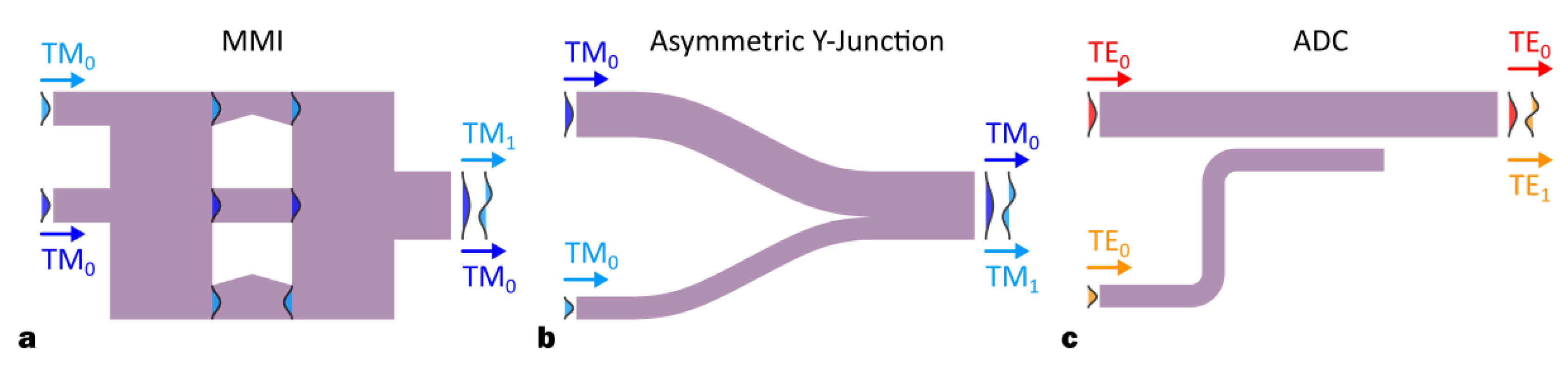
Figure 3a. The input TM0 mode from the edge port can be evenly split by a 3-dB coupler. The phase inversion is then introduced to the split beams by utilizing a π phase shifter. Finally, the two beams are combined by a cascaded mode sorter. The TM0-TM1 conversion is also carried out in the meantime. On the other hand, the input TM0 mode from the central port can directly propagate through the 3-dB coupler and mode sorter without mode conversion. This MMI-based structure can provide low insertion losses (IL < 1.8 dB), low crosstalk (XT < −20 dB) and a broad working bandwidth (BW > 60 nm) [25]. The major disadvantage is the relatively large device size (≈80 μm), which can be reduced by replacing the phase shifter with a tilted joint section [26]. The two-channel mode (de)multiplexer can also be realized by using a 2 × 2 MMI coupler (LMMI = Lπ/2) assisted with a symmetric Y-junction [27]. The designed 2 × 2 MMI coupler can evenly separate the input TE0 mode with a phase difference of −π/2 or +π/2, which can be modified to 0 or π by inserting a π/2 phase shifter. The two beams with 0/π phase difference are then combined and converted to TE0/TE1 modes by a symmetric Y-junction. The simulation results show low losses (IL < 0.1 dB), low crosstalk (XT < −17 dB) and a broad bandwidth (BW > 100 nm). Compared with the previous MMI-based structures, this improved design can provide a simplified configuration as well as a better performance. However, the MMI/Y-junction structure still suffers from a relatively large footprint (≈50 μm). The device size can be effectively reduced to ≈36 μm by using a subwavelength grating (SWG) metamaterial slab with engineered refractive index and mode dispersion [28]. Apart from the smaller footprint, this SWG-based structure also has a superior performance compared with the aforementioned MMI-based design. The working bandwidth can be as large as 300 nm, while low losses (IL < 0.84 dB) and low crosstalk (XT < −20 dB) can also be maintained.
The second type of silicon mode (de)multiplexer is based on the asymmetric Y-junction. The mostly commonly used Y-junctions are symmetric [60,61,62,63], which have been extensively applied for power splitting/combining and signal broadcasting. The asymmetric Y-junction is less common, which is usually characterized by the non-identical arms in term of the waveguide width. For the asymmetric Y-junction, the incident light from a single arm will be coupled into a higher-order mode with the closest effective index [64]. The mode conversion factor (MCF) can be used to determine the structural parameters of an asymmetric Y-junction [65]:
MCF = |βa − βb|/θdγab,
γab = 0.5[(βa + βb)2 − (2k0nc)2]1/2,
where βab is the propagation constant for the fundamental mode in the wider/narrower arm, θd is the divergence angle, k0 is the free-space wavenumber, nc is the cladding refractive index. The mode-selective coupling occurs when MCF > 0.43 [65]. This unique characteristic of asymmetric coupling offers a great opportunity for mode (de)multiplexing. The asymmetric Y-junctions are initially studied on low-contrast material platforms, e.g., silica waveguide or silica fiber [64,66,67]. In [29], a two-channel silicon mode (de)multiplexer was demonstrated based on asymmetric Y-junctions, as shown in Figure 3b. For such a design, the input TM0 mode in the wider/narrower arm excites the first even/odd mode in the “stem”, i.e., TM0/TM1. The measurement results exhibit low losses (IL < 1.5 dB) and low crosstalk (XT < −30dB) for the fabricated asymmetric Y-junction. However, this Y-junction-based design is quite sensitive to the structural parameters, especially to the divergence angle (θd), since the mode-selective condition (MCF > 0.43) will no longer be satisfied when θd is changed. Another drawback is the relatively narrow working bandwidth caused by the coupling-induced interference between two arms. These problems could be solved by introducing the novel shortcut-to-adiabaticity (STA) method [68]. The parametric sensitivity and interference effect can be dramatically inhibited for the asymmetric Y-junction by varying waveguide widths and waveguide separation along the arm section [69], leading to a robust and broadband mode (de)multiplexing. As an alternative, the two-channel mode multiplexer can also be realized by exploiting a “two-step” strategy [30]. The TE0 mode in the wide/narrow arm is first converted to the symmetric/asymmetric super-mode (i.e., TES/TEAS) by using an adiabatic coupler [70,71]. Such TES/TEAS super-modes are then injected into the “stem”, which will directly excite TE0/TE1 modes in the multi-mode bus waveguide. Here, the super-modes are used as a transition between the input fundamental modes and the output higher-order modes, which prevents the undesired crosstalk caused by direct mode conversion. The mode (de)multiplexer with low losses (IL < 1 dB) and low crosstalk (XT < −20 dB) was experimentally achieved over a broad wavelength span from 1.525 μm to 1.60 μm (BW ≈ 75 nm). Moreover, for this design, the high-performance can be preserved even if the structural parameters are deviated over a >±30 nm range. There are also some other types of Y-junction-based MDMs, such as ones based on partially etched slab waveguides [31].
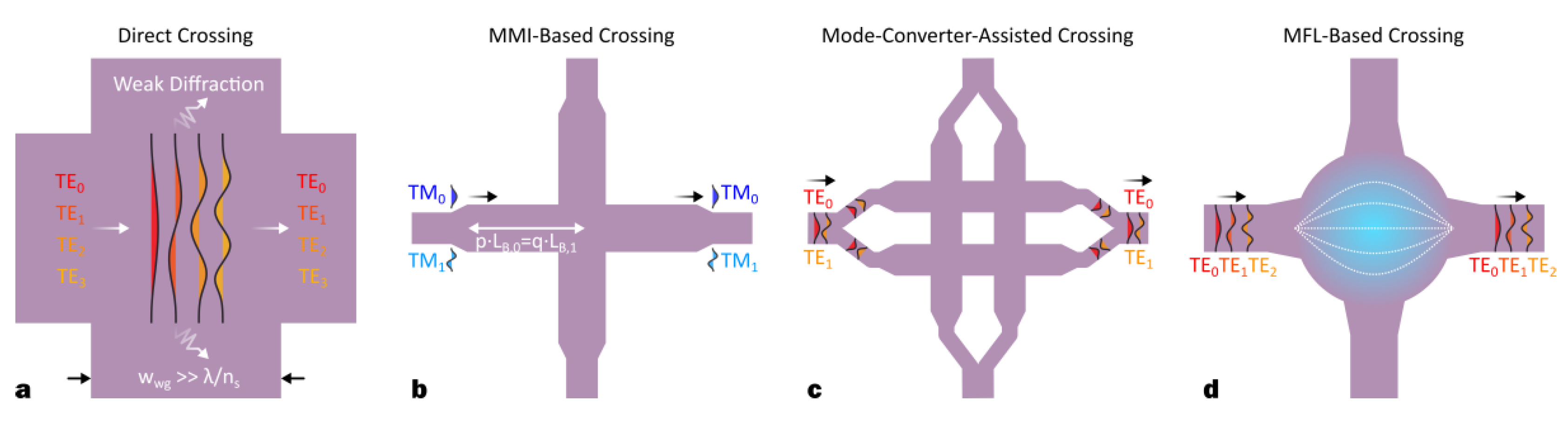
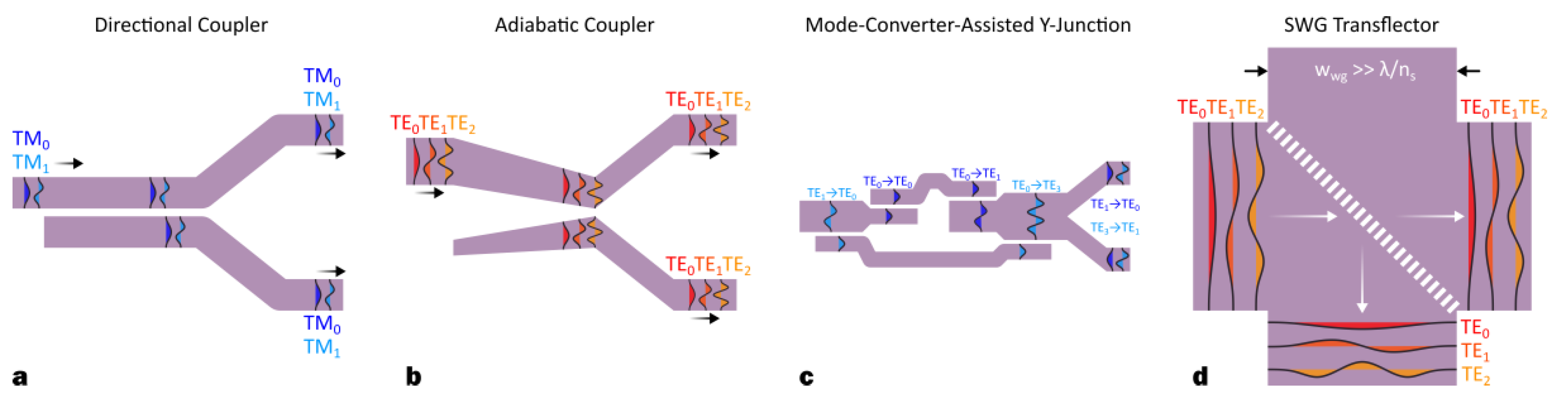
However, there are some clear disadvantages of the silicon mode (de)multiplexers based on MMIs or asymmetric Y-junctions. For instance, the MMI-based structures usually suffer from intrinsically high insertion losses due to the strong scattering at the input/output port, while for the Y-junction-based structures, a small feature size is usually required at the position where two arms are converged. The ADC has been widely considered as a better choice for realizing high-performance silicon mode (de)multiplexers, which is comprised of two closely placed waveguides with different core widths (see Figure 4c). Here, we show a design example for an ADC-based two-channel mode (de)multiplexer considering the first two TE modes (i.e., TE0/TE1). The input TE0 mode in waveguide #0 can be coupled to the output TE1 mode in waveguide #1 through evanescent coupling (see the inset of Figure 4a). The complete TE0–TE1 coupling can be obtained only if the phase-matching and critical coupling conditions are simultaneously satisfied [72]. 
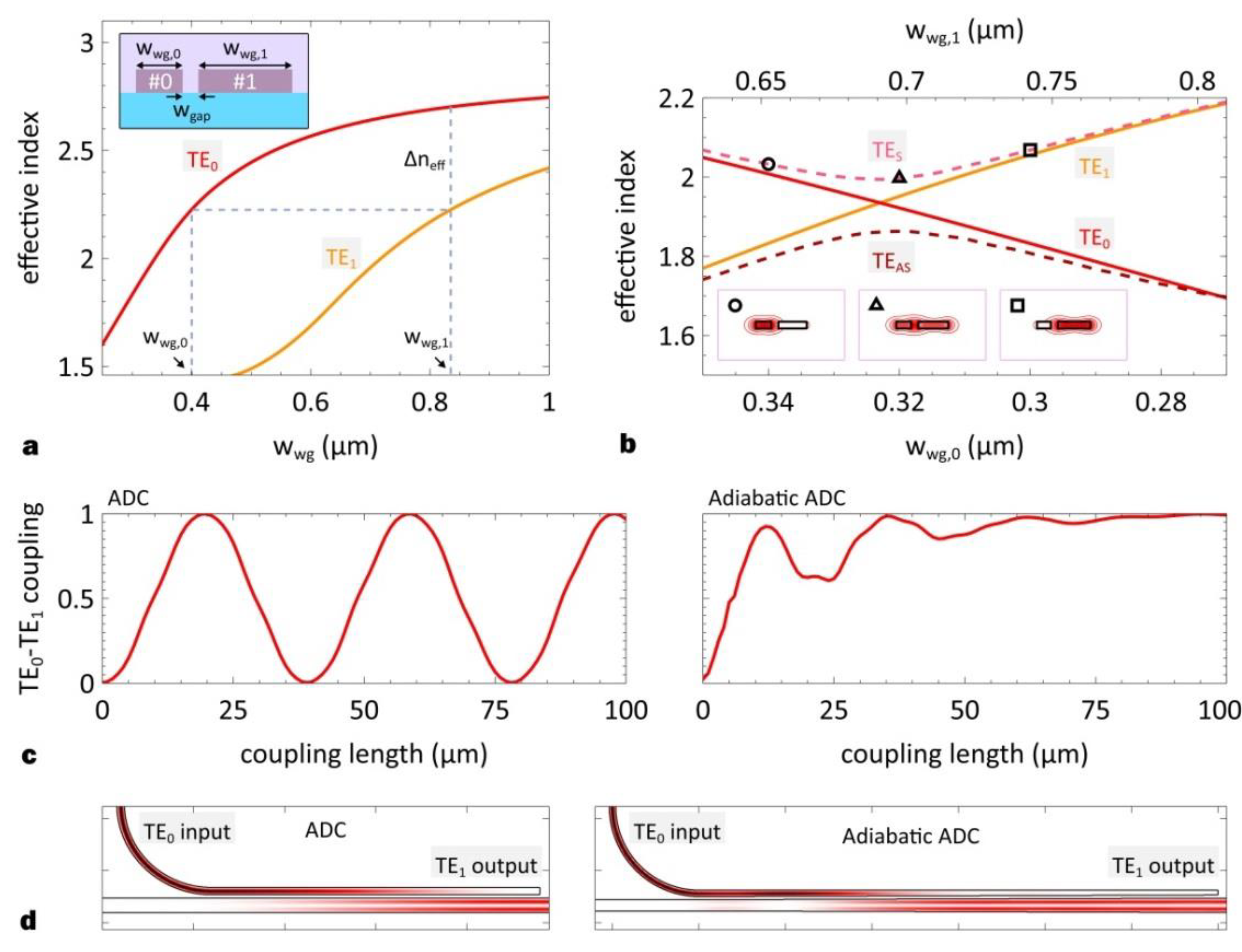
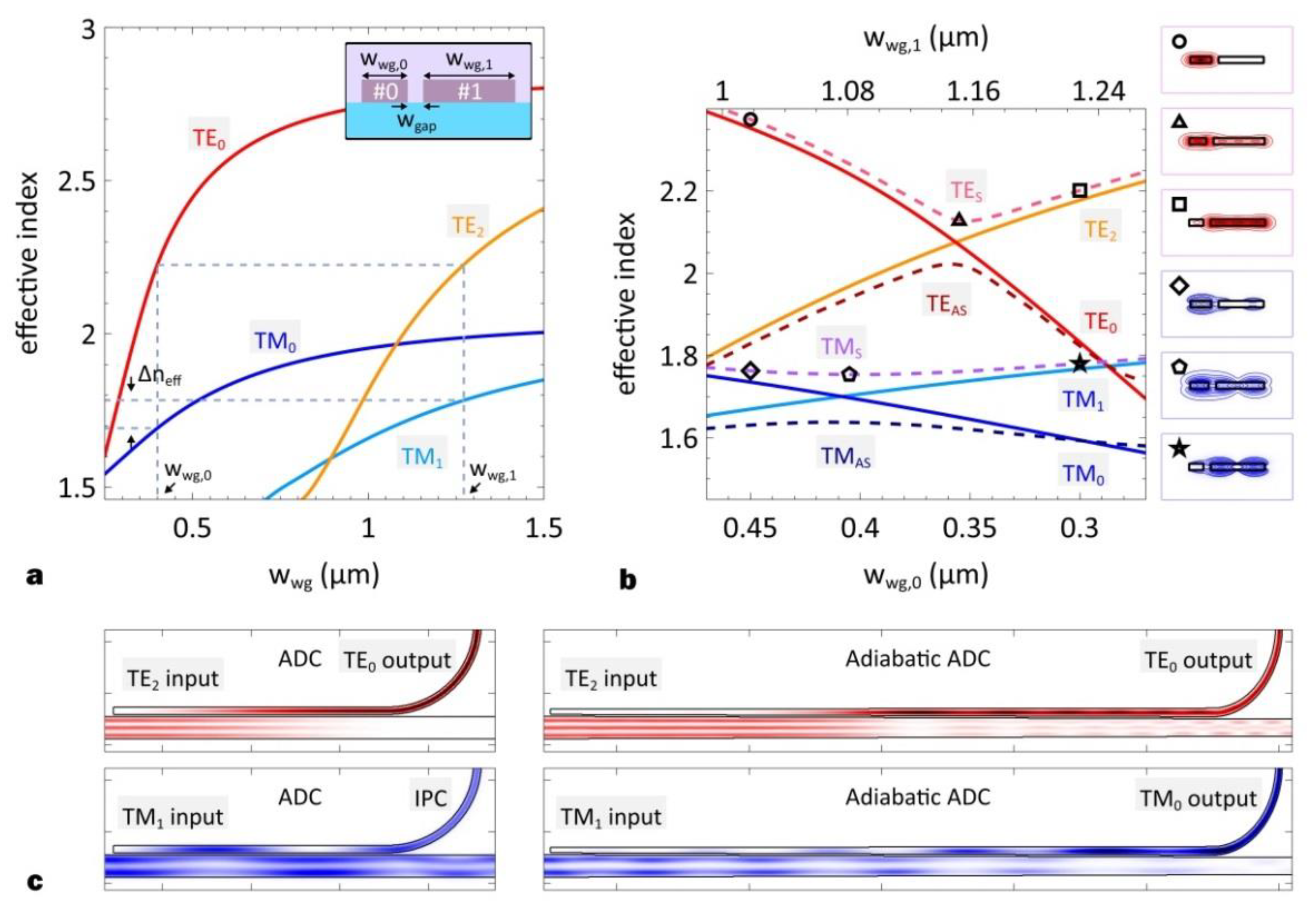
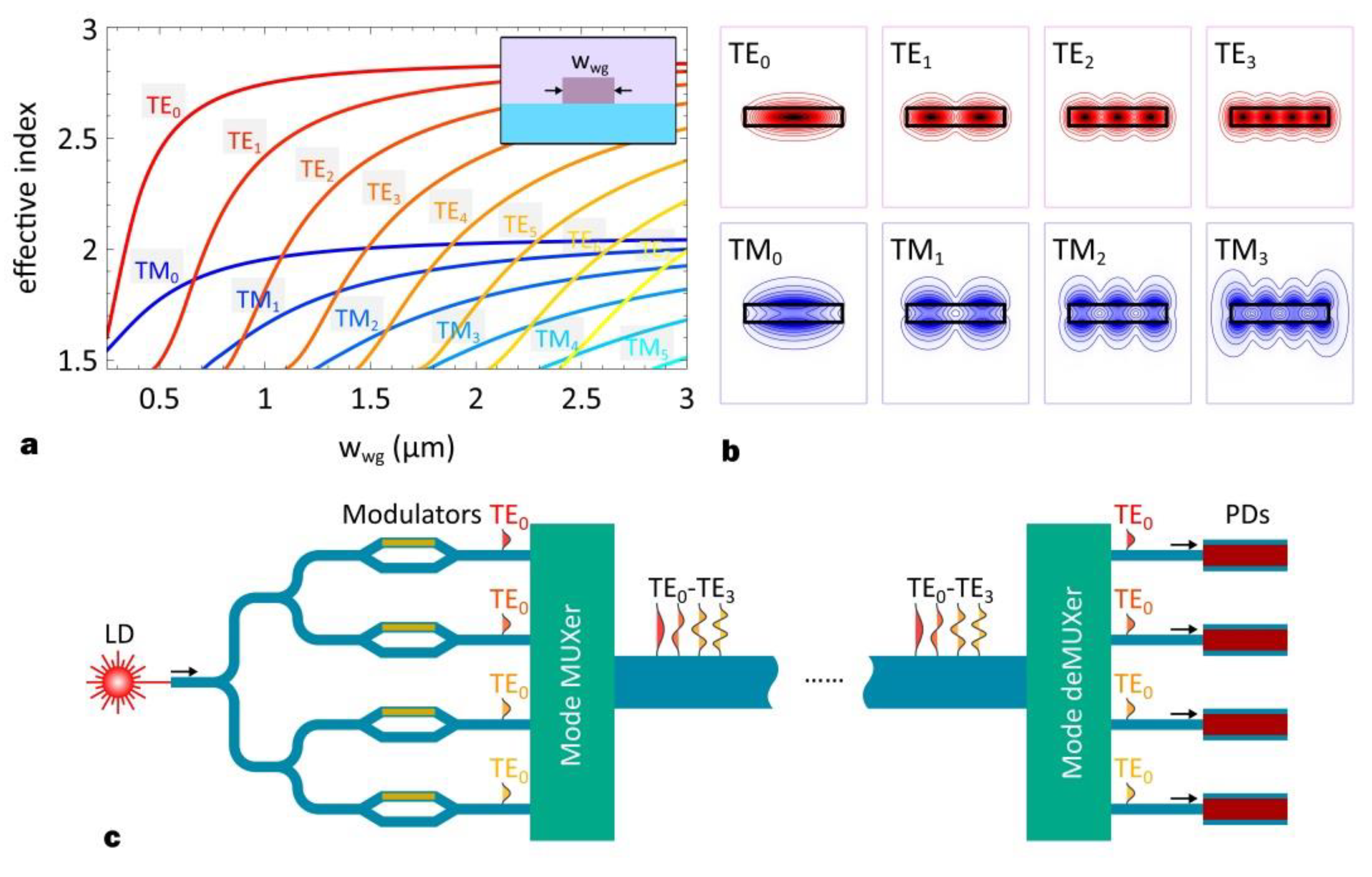
Figure 4a shows the calculated effective indices for TE0 and TE1 modes in a SOI waveguide with core width varying from 250 nm to 1 μm. Here, we consider the 220-nm-thick SOI platform with a SiO2 upper cladding. The core width is chosen to be wwg,0 = 400 nm for waveguide #0 to fulfill the single-mode condition operating at 1.55-μm wavelength. Thus, one can easily determine the core width for waveguide #1 as wwg,1 = 835 nm, so that the effective indices are matched between TE0 and TE1 (see the dashed lines in Figure 4a). After that, we calculate the TE0–TE1 coupling ratio with varied coupling length, as shown in the left panel of Figure 4c. Here, the gap width is chosen to be wgap = 200 nm. It can be observed that the curve is sinusoid-like and the first critical coupling length is ≈18 μm. The light propagation profile is then calculated for the optimized ADC, as shown in the left panel of Figure 4d. From the profile, one can observe the efficient TE0–TE1 mode conversion and the complete power transfer from waveguide #0 to waveguide #1. Additionally, the phase-matching condition is satisfied only between TE0 in waveguide #0 and TE1 in waveguide #1, so TE0 mode can directly inject into waveguide #1 without evanescent coupling or mode conversion (see the dashed lines in Figure 4a), enabling a dual-mode (de)multiplexing.
However, for the silicon ADCs, the phase-matching and critical coupling conditions can be perfectly fulfilled only at the central wavelength due to the strong waveguide dispersion, leading to a restricted working bandwidth. The bandwidth could be expanded by using SWGs [32,33,34] or hybrid plasmonics [35], but these structures are not easy to realize. Furthermore, a stringent fabrication is always required for ADCs since the mode conversion and light-coupling processes are quite sensitive to the parametric deviations, which could significantly increase the crosstalk [73]. These obstacles can be tackled by utilizing adiabatic ADCs [36,37]. The idea is to introduce an adiabatic mode evolution by gradually changing the core widths (wwg,0, wwg,1) along the coupling section. Here, we show a design example for an adiabatic TE0–TE1 ADC with linearly varied core widths. For waveguide #0, the core width is linearly varied from wwg,0 = 350 nm to wwg,0 = 270 nm, while for waveguide #1, the core width is linearly varied from wwg,1 = 630 nm to wwg,1 = 810 nm. Here, the gap width is set to be wgap = 200 nm. Figure 4b shows the calculated effective indices for TE0/TE1 modes in waveguide #0/#1 (see the solid lines) and TES/TEAS super-modes in the dual-core ADC (see the dashed lines). From the curves, one can find a critical point where the effective indices are matched between TE0 and TE1 (wc,0 = 325 nm, wc,1 = 690 nm). The TES effective index approaches the TE0 effective index when wwg,0 > wc,0 and wwg,1 < wc,1, indicating that the light power is mainly supported by the TE0 mode in waveguide #0, as shown in the inset of Figure 4b. Around the critical point, both TE0 and TE1 modes will be excited in waveguide #0/#1 (see the inset of Figure 4b), indicating the phase matching. The TES effective index approaches the TE1 effective index when wwg,0 < wc,0 and wwg,1 > wc,1, indicating that the light power is mainly supported by TE1 mode in waveguide #1, as shown in the inset of Figure 4b. Thus, the input TE0 mode in waveguide #0 can be gradually “pushed” into waveguide #1 by slowly varying the core widths. The TE0–TE1 mode conversion is also attained in the meantime. To demonstrate this, we calculate the TE0–TE1 coupling ratio with various coupling lengths, as shown in the right panel of Figure 4c. For the conventional ADC, the coupling ratio periodically changes with the coupling length, while for the adiabatic ADC, the coupling ratio monotonically reaches 100% when the coupling length is long enough (>100 μm), indicating that the mode conversion is an adiabatic process. One might find some ripples in the coupling–ratio curve, which is mainly induced by the slight interference effect. The light propagation profile is then calculated for the optimized adiabatic ADC, as shown in the right panel of Figure 4d. The complete mode conversion can be observed from the calculated profile. In [38], the silicon adiabatic ADC was demonstrated for the first time. The measurement results show low losses (IL < 0.3 dB) and low crosstalk (XT < −16 dB) over a 100-nm wavelength band. The counter-tapered ADC was proposed and demonstrated in [39] to further enhance the working bandwidth (BW >180 nm) and relax the fabrication stringency. Later, the taper-etched ADC was proposed as a highly efficient mode (de)multiplexer [40]. Low losses (IL < 1.3 dB) and low crosstalk (XT < −26 dB) were also experimentally demonstrated. However, adiabatic coupling is always accompanied with a long coupling length (see Figure 4c) and a large footprint. Note that the gap width is fixed for the aforementioned ADCs, so the coupling strength is a constant for these structures. The recent studies have shown that a broad bandwidth can be ensured even with quite a short coupling length by simultaneously changing core width (wwg,0, wwg,1) and gap width (wgap) [41]. In [42], a short and robust silicon ADC was realized by utilizing the novel STA method. A detailed description of an STA-based coupler can be found in [74]. For this optimal design, the coupling length is as short as 50 μm, while ultra-low crosstalk (XT < −30 dB), ultra-broad bandwidth (BW > 150 nm) and ultra-large fabrication tolerance (±50 nm) can still be ensured.
From the above discussions, the structures based on MMIs, asymmetric Y-junctions and ADCs all show some degrees of advantages in achieving mode (de)multiplexing. However, all these mode (de)multiplexers are not scalable, which means that these designs can only support a few modes (typically two modes). The scalable mode (de)multiplexers are desired in the MDM systems, which can be built by successively connecting several Y-junctions [75,76] or ADCs [77,78,79,80,81,82]. 
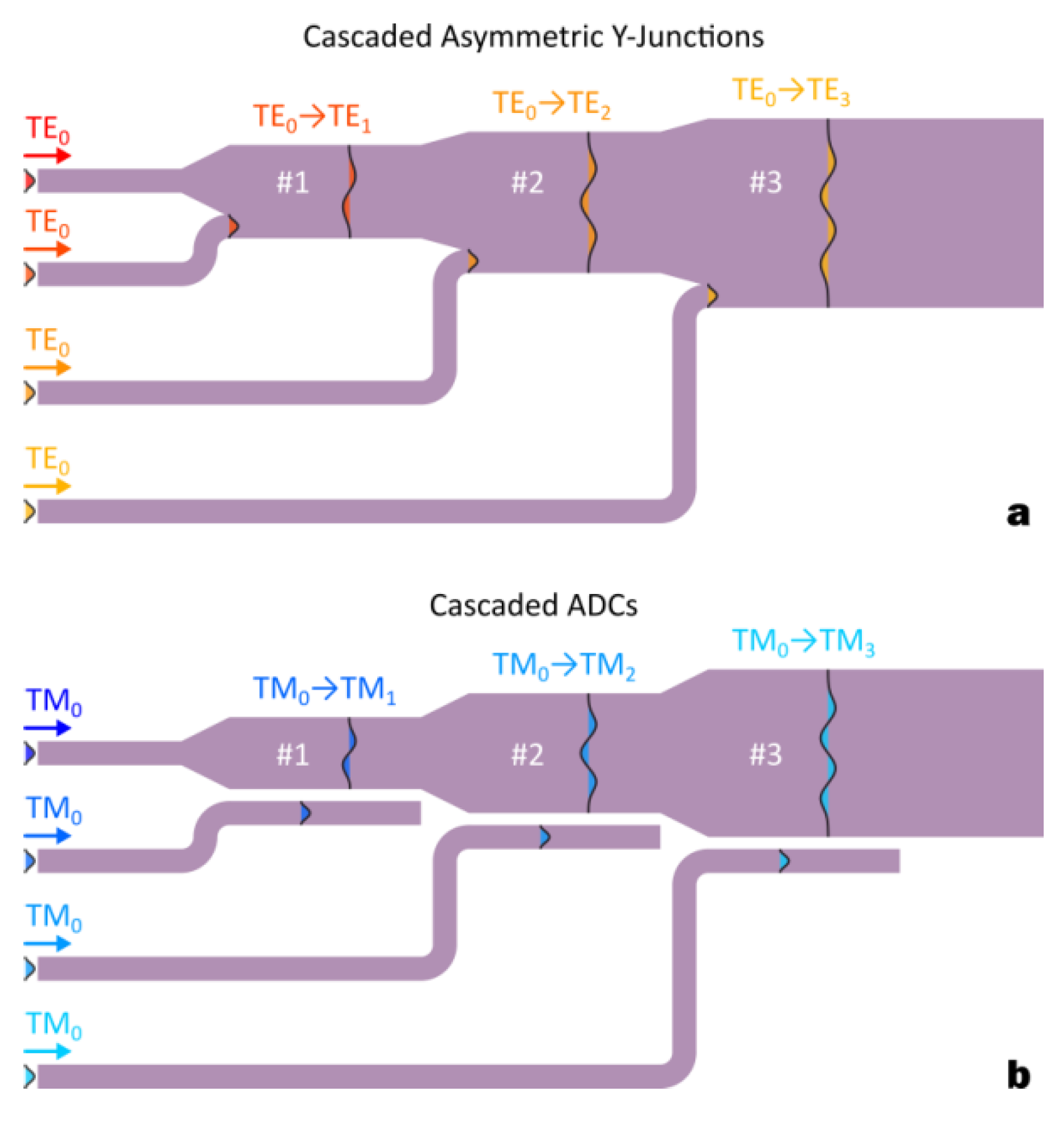
Figure 5a shows the configuration of a typical four-channel mode (de)multiplexer using the cascaded asymmetric Y-junctions [75]. Three higher-order TE modes (i.e., TE1, TE2, TE3) can be independently excited by several different Y-junctions, while the fundamental TE mode, i.e., TE0, is directly injected into the multi-mode bus waveguide. The arm widths are carefully chosen so that the mode-selective condition is satisfied for only one higher-order mode in each Y-junction. In [76], W. Chen et al. reported a three-channel MDM with cascaded asymmetric Y-junctions on silicon. The experimental results exhibit crosstalk of XT ≈ −10 dB for the first three TE modes (i.e., TE0–2). Nevertheless, the cascaded asymmetric Y-junction still seriously suffers from significant insertion losses (IL > 5 dB) and the small feature size at the junction’s tip. In contrast, the cascaded ADCs are broadly considered as a more promising candidate for mode (de)multiplexing based on the best overall performances. In 2013, the first cascaded ADC-based silicon mode (de)multiplexer was reported by D. Dai et al. [77], as illustrated in Figure 5b. In ADC #i, the phase matching is satisfied only between TM0 and TMi, so the input TM0 mode can converted to TMi mode and multiplexed into the multi-mode bus waveguide, while the other higher-order modes (i.e., TMj, j < i) will go through the coupling section with negligible losses. Additionally, TM0 mode is directly launched from the multi-mode bus waveguide without evanescent coupling or mode conversion. In this way, a four-channel mode (de)multiplexer can be built by cascading three ADCs with adiabatic tapers as connectors in between. Compared with the cascaded Y-junctions, the proposed cascaded ADCs can provide a larger feature size (>300 nm), lower insertion losses (IL < 1 dB) and lower crosstalk (XT < −23 dB). However, the experimental results also show a relatively narrow working bandwidth (BW ≈ 20 nm), which can be further improved (BW > 100 nm) by exploiting adiabatic coupling [39,78,79] or ultra-thin waveguides [80]. Moreover, recent research also shows that the crosstalk of cascaded ADCs can also be further mitigated by exploiting coherence detection [83]. In Table 1, we summarize the reported silicon mode (de)multiplexers. It can be seen that the various silicon mode (de)multiplexers have been realized with low losses, low crosstalk and a broad bandwidth. In theory, the mode capacity can be expanded at will by simply cascading more ADCs; however, an extremely long coupling length would be needed to achieve the conversion to a very high-order mode, which could lead to a large and complex device layout as well as increased crosstalk. The issue could be addressed by employing SWG waveguides with an engineered index [81,82]. However, the fabrication of SWG is immature given its subwavelength feature size. To further expand the capacity, a more effective solution is the wavelength/polarization/mode hybrid (de)multiplexing that combines multiple dimensions of light. A discussion about silicon hybrid (de)multiplexers will be given in Section 2.2.

2.2. Silicon Hybrid (De)Multiplexers

As discussed above, mode (de)multiplexing can efficiently enhance the link capacity, but it is still quite difficult to (de)multiplex very high-order modes in a multi-mode bus waveguide. Therefore, it is more cost effective to build multi-dimensional on-chip communication systems by combining MDM with WDM [86,87,88,89,90,91,92,93,94,95] and PDM [96,97,98,99,100].
The wavelength/mode hybrid (de)multiplexers are able to simultaneously manipulate signals carried by wavelength and mode channels. WDM/MDM hybrid systems could be realized by using some special mode (de)multiplexers with strong wavelength-selectivity, e.g., asymmetric Y-junctions [86], grating-assisted ADCs [87], photonic crystals [88] and asymmetric micro-ring resonators [89,90]. However, such wavelength-selective mode coupling is usually quite sensitive to parametric deviations, which make it difficult to align each wavelength/mode channel. A more general architecture is to cascade the broadband mode (de)multiplexers (e.g., cascaded ADCs) with the conventional wavelength (de)multiplexers, such as arrayed waveguide gratings (AWGs) [91,92] and micro-ring resonators (MRRs) [94,95], as summarized in
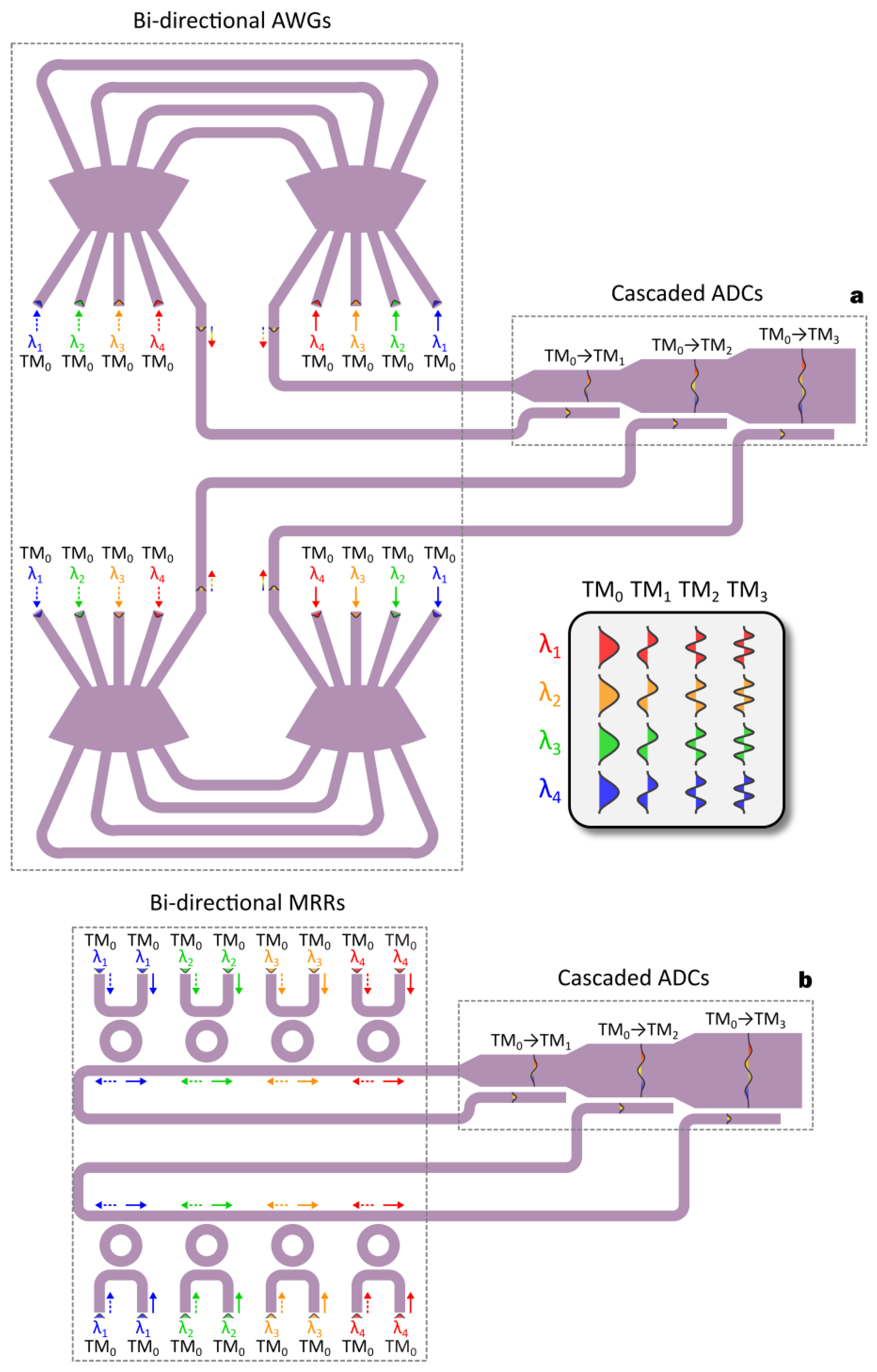
 Figure 6.
The silicon AWGs are most commonly used in the dense wavelength division-multiplexing (DWDM) systems because of the large free-spectral range (FSR) and small channel spacing [101,102,103,104,105,106,107], showing great potential for large-scale hybrid (de)mulitplexing. In [91], a 64-channel WDM/MDM hybrid system was demonstrated on silicon by cascading four identical 16-channel AWGs with a four-channel mode (de)multiplexer. For each AWG, sixteen wavelength carriers are multiplexed into a single-mode waveguide with TM0. These four waveguide channels are then converted to TM0-TM3 and multiplexed into a multi-mode bus waveguide, which makes a total link capacity of 64 (16 × 4). For such a structure, the insertion losses and crosstalk were measured to be IL≈7 dB and XT ≈ −10 dB, respectively. It should be noted that the AWGs can be bi-directional, which means that two 1 × N AWGs can be replaced by one (N + 1) × (N + 1) AWG with equivalent functionalities [101], as shown in Figure 6a. This idea was implemented to realize an improved wavelength/mode hybrid (de)multiplexer with an AWG number reduced to half [92]. The measurement results show insertion losses of IL ≈ 5 dB and crosstalk of XT ≈ −14 dB for a 64-channel WDM/MDM hybrid system. Nevertheless, the device footprint is still quite large (a few millimeters) for AWG-based wavelength/mode hybrid (de)multiplexers even if bi-directional configurations are applied. As an alternative, the cascaded MRRs are also popular for WDMs because of the low insertion losses, high extinction ratios and, especially, the compact device sizes [108,109,110]. Moreover, according to the tight-binding model [111], the top-flattened transmission responses can be realized by simply cascading several side-coupled MRRs in a serial [112]. Additionally, both clockwise and counterclockwise propagations are allowed in MRRs, so the bi-directional configurations are also applicable, as illustrated in Figure 6b. In [94], a 32-channel WDM/MDM hybrid system was demonstrated on silicon by cascading two sets of bi-directional eight-channel MRR arrays with a four-channel mode (de)multiplexer. For the fabricated device, the insertion losses were measured to be IL < 4.5 dB while the crosstalk was measured to be XT < −18dB. The insertion losses and crosstalk can be further reduced by adopting flat-top MRR filters [95]. We give a summary of the reported silicon wavelength/mode hybrid (de)multiplexers in Table 2. It can be seen that, for most of the reported structures, the wavelength channels still outnumber the mode channels, which gives rise to the system cost and layout complexity. Hence, it is necessary to reduce the wavelength channels further by introducing TE/TM polarizations as a third dimension. Furthermore, coarse wavelength-division multiplexing (CWDM) with a larger channel spacing (> 20 nm) could also be helpful to enhance the stability and lower the cost [93,113,114,115,116,117].
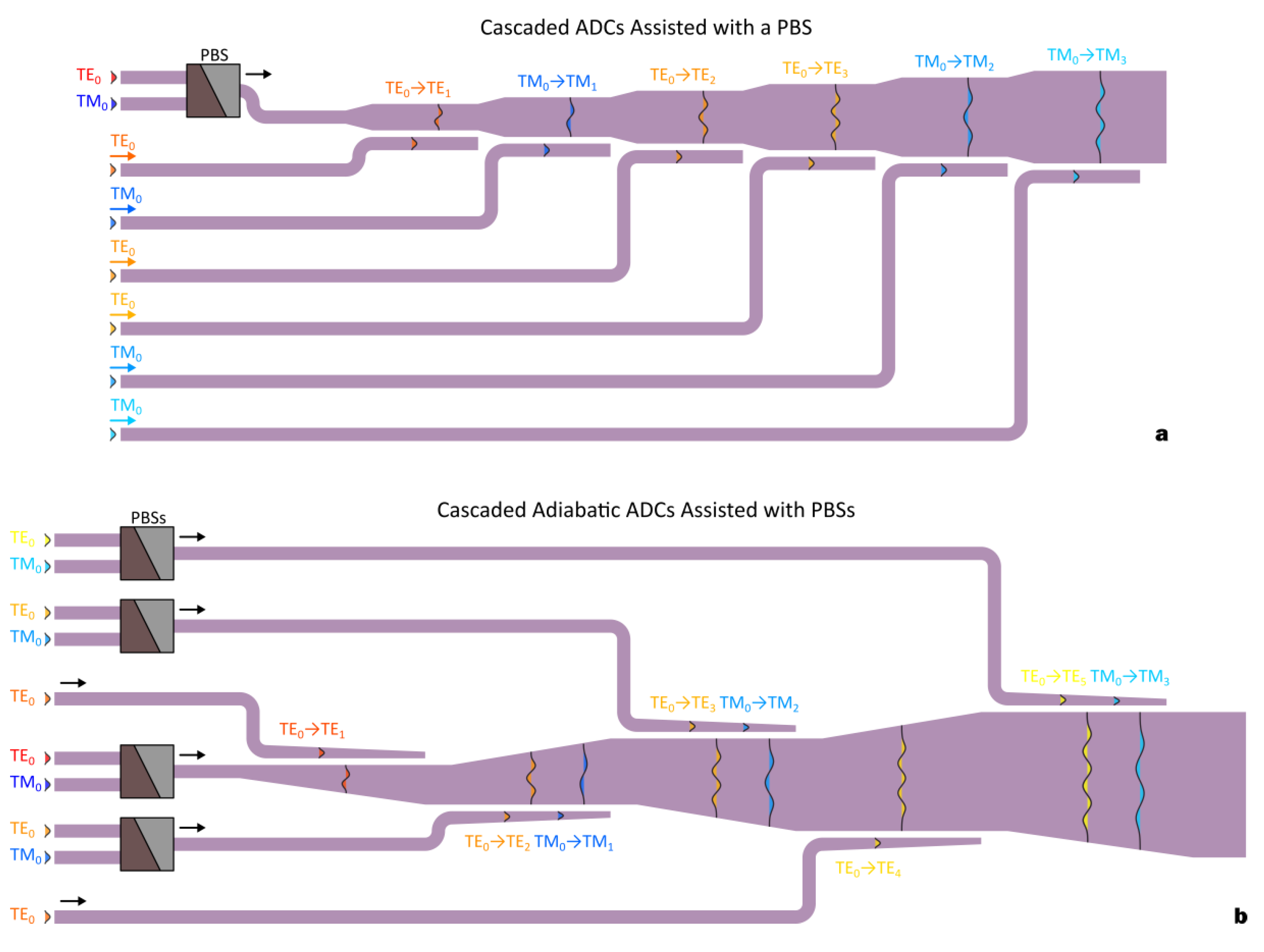
The polarization/mode hybrid (de)multiplexers are able to handle multiple mode channels with dual polarizations. One straightforward scheme is to directly cascade the two groups of ADCs designed for TE and TM modes, respectively, as illustrated in Figure 7a. In [96], an eight-channel polarization/mode hybrid (de)multiplexer was demonstrated on silicon with the first four TE/TM modes (i.e., TE0–3 and TM0–3). The higher-order modes (i.e., TE1–3 and TM1–3) are excited by using the cascaded ADCs, while TE0 and TM0 modes are coupled into the multi-mode bus waveguide by using a polarization beam splitter (PBS). The experimental results exhibit insertion losses of IL ≈ 2dB and crosstalk of XT ≈ −10 dB over a 30-nm bandwidth. For such polarization/mode hybrid (de)multiplexers, the measured crosstalk is much higher compared with the conventional mode (de)multiplexers working on a single polarization [77]. Such a phenomenon is mainly due to the undesired inter-polarization crosstalk (IPC) at the receiver terminal. Here, we show a design example to illustrate this effect. We calculate the effective indices for TE0 and TE2 modes in the 220-nm-thick SOI with SiO2 cladding, as shown in Figure 8a. The waveguide widths are chosen to be wwg,0 = 400 nm and wwg,1 = 1.27 μm to meet the phase-matching condition between TE0 and TE2 at a 1.55-μm wavelength. The gap width is chosen to be wgap = 150 nm. The coupling length is then optimized to be 15.5 μm to achieve critical coupling. Thus, the input TE2 mode can be completely demultiplexed from the multi-mode bus waveguide with negligible residual power, as shown in Figure 8c. Unfortunately, for these optimal parameters, the effective indices are also quite close between TM0 and TM1 (see the dashed lines in Figure 8a). As a result, part of the input TM1 mode will also be extracted by the ADC optimized for TE0–TE2 conversion (see Figure 8c), leading to the significant IPC. The IPC could be reduced by optimizing the structural parameters to achieve a polarization-selective mode coupling [96,97,98]. However, this methodology always leads to a relatively narrow working bandwidth and a significant parametric sensitivity. Another possible solution is to cascade the polarizers to filter out the undesired polarizations [99], but polarization filtering will give rise to the total insertion losses [118,119,120,121,122,123,124,125,126,127,128].
The IPC problem can be addressed by exploiting the cascaded adiabatic ADCs, as shown in Figure 7b. The idea is to optimally choose the core widths for each ADC, so that both TE and TM polarizations can be completely extracted from the multi-mode bus waveguide. The decoupled TE0 and TM0 modes are then separated by a PBS. To illustrate this idea, we show a design example of adiabatic ADC considering both TE0–TE2 and TM0-TM1 mode conversions. For waveguide #0, the core width is linearly varied from wwg,0 = 270 nm to wwg,0 = 470 nm, while for waveguide #1, the core width is linearly varied from wwg,1 = 1.27 μm to wwg,1 = 990 nm. Here, the gap width is set to be wgap = 150 nm. Figure 8b shows the calculated effective indices for TE0/TE2/TM0/TM1 modes (see the solid lines) and TES/TEAS/TMS/TMAS super-modes (see the dashed lines). Over this width variation range, the phase matching can be achieved for both TE0–TE2 and TM0-TM1 at different critical widths (see the curve intersections in Figure 8b). Thus, the input TE2 and TM1 modes can be simultaneously “pushed” into the single-mode waveguide (see the inset of Figure 8b). We then calculate the light propagation profiles for the optimized ADC when TE2 and TM1 modes are launched, as shown in the right panel of Figure 8c. Here, the coupling length is chosen to be 50 μm to satisfy the adiabatic condition. From the profiles, one can observe the efficient mode conversion and complete power transfer for both TE and TM polarizations. This idea was implemented to realize a 10-channel polarization/mode hybrid (de)multiplexer working with the first six TE and four TM modes (i.e., TE0–5, TM0–3). The experimental results show low losses (IL < 1.8 dB) and low crosstalk (XT < −15 dB) over a 90-nm wavelength band. In Table 3, we summarize the reported silicon polarization/mode hybrid (de)multiplexers. One can see that the link capacity can be efficiently enhanced (up to 10 channels) by combining MDM and PDM technologies, while low losses (IL < 2 dB) and low crosstalk (XT ≈ −20 dB) can still the preserved over quite a broad wavelength band (BW ≈ 100 nm).
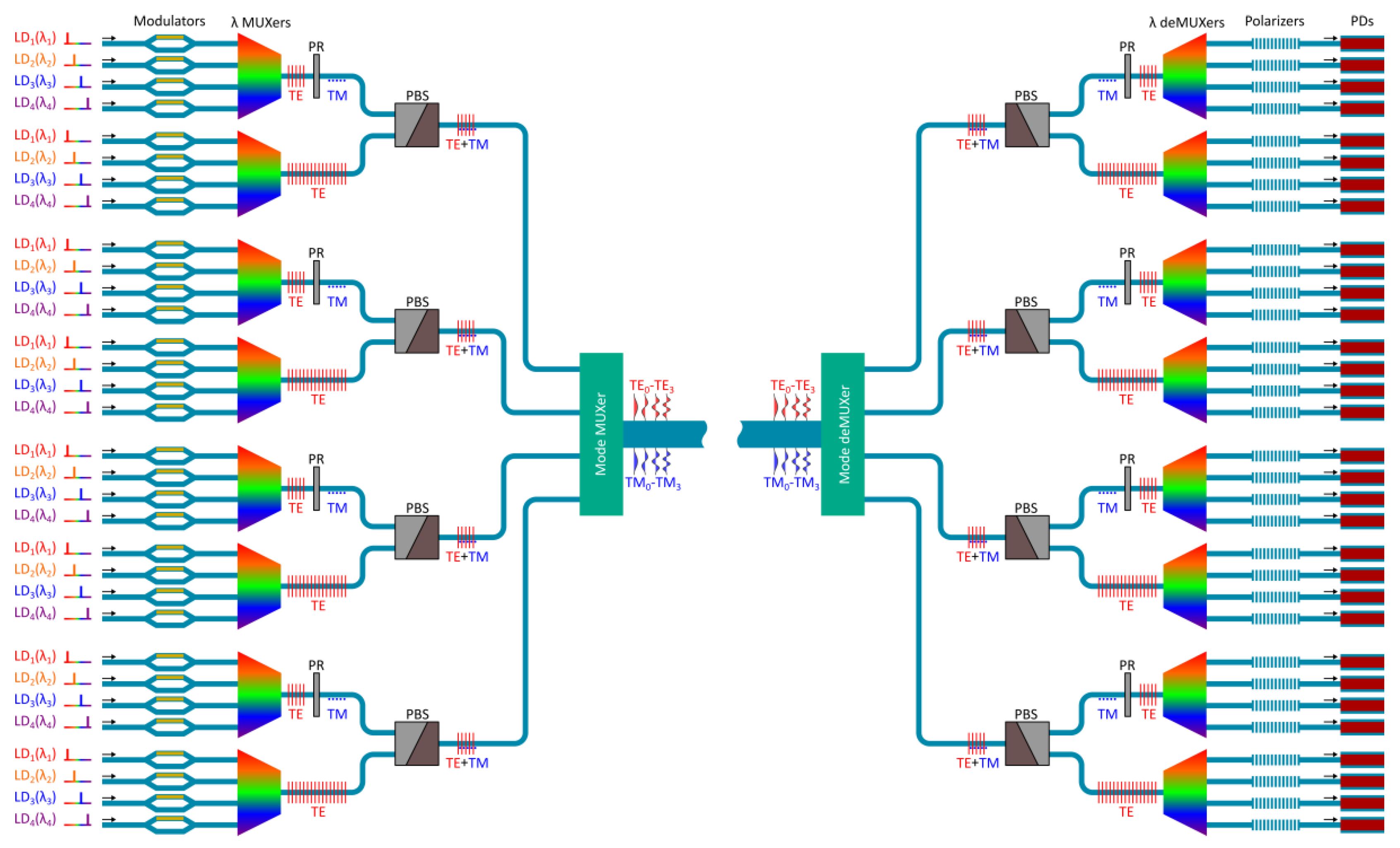
The link capacity can be dramatically scaled up by employing WDM/MDM or PDM/MDM hybrid systems. However, it is still challenging to realize WDM/PDM/MDM hybrid systems that involve all the three dimensions of light. So far, there have been only a few demonstrations on the wavelength/polarization/mode hybrid (de)multiplexing. Recently, Y. He et al. demonstrated an eight-channel hybrid (de)multiplexer with two wavelengths, two polarizations and two modes [129]. The device is based on the cascaded contra-directional couplers that assist with Bragg gratings. According to the Bragg condition, each coupling section can select a single carrier on a specific wavelength/polarization/mode channel. Nevertheless, the capacity is still restricted for this structure, and the insertion losses are also quite significant (IL ≈ 6.6 dB). Here, we propose a general configuration for the scalable WDM/PDM/MDM hybrid systems, as illustrated in Figure 9. As an example, we show a 32-channel hybrid (de)multiplexer with four wavelengths, two polarizations and four modes. At the transmitter terminal, the 32-channel carriers with TE0 are firstly coupled into eight single-mode waveguides in term of the wavelengths. Four of them are cascaded with the broadband polarization rotators [130,131,132,133,134,135,136,137,138,139,140,141] that convert TE0 to TM0. The PBSs [142,143,144,145,146,147,148,149,150,151,152,153] are then utilized to combine the orthogonal polarizations, so that the 32-channel signals can be carried by four single-mode waveguides. Finally, all the carriers are coupled into a multi-mode bus waveguide by using a polarization/mode hybrid multiplexer working on TE0–3 and TM0–3 [100]. At the receiver terminal, the 32-channel carriers are decoupled from the multi-mode bus waveguide by cascading MDM, PDM and WDM in sequence. This configuration can be used as a general architecture to build any user-defined WDM/PDM/MDM hybrid system.

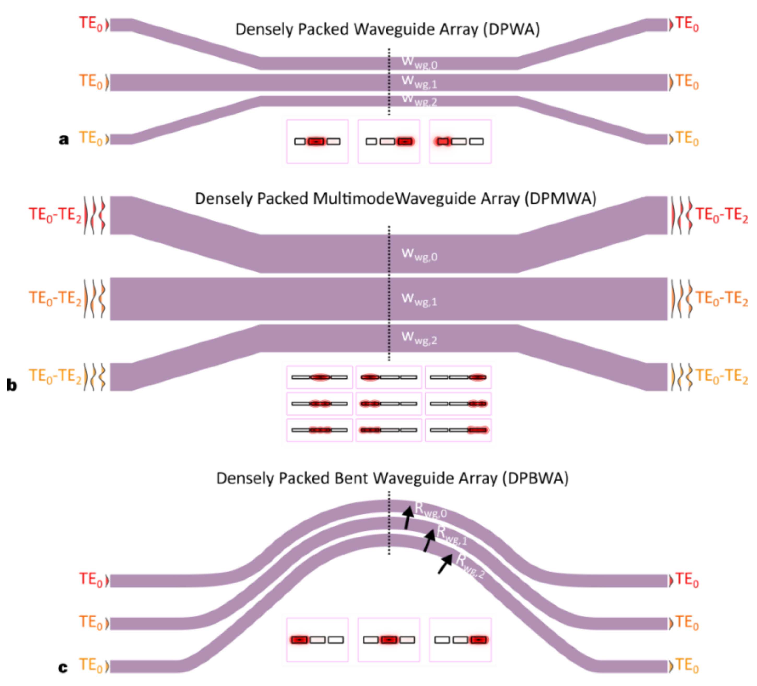
2.3. Densely Packed Waveguide Array

For the MDM system, the signals are usually carried by multiple higher-order modes in a wide multi-mode bus waveguide. However, from the above discussions, one might find that the high-performance mode (de)multiplexers are not easily realized. Instead of using the higher-order modes, the MDM can also be obtained by using the super-modes supported by several closely placed single-mode waveguides, leading to the novel concept of a densely packed waveguide array (DPWA) [154,155,156,157,158,159,160], as shown in Figure 10.
In [154], the DPWA-based MDM was proposed for the first time. The structure consists of three single-mode SOI waveguides each with different core widths and narrow gap widths in between, as shown in Figure 10a. Three super-modes can be supported by the DPWA. Unlike the conventional guided modes that are supported by a single isolated waveguide, the super-modes are supported by an array of waveguides, so the field contribution can be engineered by modifying parameters for each waveguide. If the core widths are uniform (wwg,0 = wwg,1 = wwg,2), each super-mode will have power distributions in more than one waveguide. In contrast, if the core widths are non-uniform (wwg,0 ≠ wwg,1 ≠ wwg,2), each super-mode will be well confined in a single core region due to phase mismatching (see the inset of Figure 10a). Moreover, such distinguishable distribution can be kept for all the three super-modes even if the gap widths are deep-subwavelength (wgap = 100 nm), so the waveguide array can be regarded as a multi-mode bus waveguide with a small lateral-dimension. For DPWA, mode (de)multiplexing can be achieved by using a simple fan-in/out structure since the mode profiles are perfectly matched between super-modes and individual TE0 mode, leading to a simple device layout. Such DWPA-based MDM can provide low losses (IL < 0.1 dB), low crosstalk (XT < −20dB) and a broad bandwidth (BW >100 nm). Furthermore, the DPWA can also be used as a sub-cell in an even larger waveguide super-lattice structure [155,156].
For DPWA-based MDM, the total capacity can be expanded further by introducing dual polarizations or higher-order modes [157,158]. In [157], a five-channel polarization/mode hybrid multiplexing was demonstrated with a DPWA supporting three TE super-modes and two TM super-modes. The fabricated device exhibits low losses (IL < 0.6 dB) and low crosstalk (XT < −15 dB) over an 80-nm wavelength span. However, the scalability is limited for this design since there are only two orthogonal polarizations. The densely packed multi-mode waveguide array (DPMWA) was proposed to break the limit [158]. The DPMWA structure is comprised of three parallel multi-mode waveguides each supporting three TE modes (i.e., TE0–2), leading to a transmission capacity of nine super-modes, as shown in Figure 10b. Each super-mode can be effectively restricted within a single core region (see the inset of Figure 10b) because of the core width differences. To realize the mode multiplexing, the higher-order modes are firstly excited in each waveguide by using the cascaded ADCs; the excited higher-order modes can directly convert to the corresponding super-modes through a simple butt-coupling process. From the experimental results, one can find low losses (IL < 1 dB) and low crosstalk (XT < −15 dB).
For DPWA, large effective-index difference is always desired between the adjacent cores in order to reduce the crosstalk in the MDM system. Phase mismatching can be achieved by changing the core widths, as discussed above. However, the width variation design requires a high-resolution fabrication process. An alternative is to engineer the waveguide curvature. For the bent waveguides, the phase-matching condition can be written as [161]:
neff,0R0 = neff,1R1,
where neff,0 and neff,1 are the effective indices, R0 and R1 is the bending radii. From the equation, it can be seen that the adjacent cores can be phase-mismatched even with the same core widths (neff,0 = neff,1) as long as the bending radii are different (R0 ≠ R1), which leads to the densely packed bent-waveguide array (DPBWA), as shown in Figure 10c. In [159], a 16-channel DPBWA-based MDM was demonstrated with low losses (IL < 1 dB), low crosstalk (XT < −20 dB) and a broad bandwidth (BW > 80 nm). All the waveguides in the proposed DPBWA have the same core widths, which makes the DPBWA quite easy to fabricate. In [160], a similar super-lattice structure was also demonstrated with low losses (IL < 0.5 dB) and low crosstalk (XT < −19.5).
The working performances for the reported silicon DPWAs are summarized in Table 4. One can see that the major advantage of the DPWA/DPMWA/DPBWA-based MDM is the large capacity (up to 16 channels) since the channel number can be easily scaled up by involving more waveguides. The losses and crosstalk are also quite weak due to the convenient mode (de)multiplexing. We believe that the novel DPWA can offer great opportunities for high-density on-chip optical transmissions.

3. Silicon Multi-Mode Routing Devices

A complex topology is always desired to boost the performance of an on-chip data link. For example, Figure 11 shows the configuration for the multi-mode interconnects in a micro-processor with five cores. From the configuration, one can find that a situation has arisen where multi-mode routing devices are necessary to facilitate the multi-mode network; also, the multi-mode routing devices should fall into three categories: multi-mode bends, multi-mode crossings and multi-mode splitters. The multi-mode bends enable light transmission with a sharp curvature, which will be discussed in Section 3.1. Another essential building block is the multi-mode crossing, which enables simultaneous cross-over propagations for multiple higher-order modes. The silicon multi-mode crossings will be reviewed in Section 3.2. Multi-mode splitters are also necessary to realize the broadcast topology, which will be discussed in Section 3.3.

3.1. Silicon Multi-Mode Bends

The waveguide bend is a basic component that constitutes the cornerstone of a photonic integrated circuit. The SOI waveguide can support an extremely small bending radius [162,163,164,165], taking advantage of its ultra-high-index contrast. However, most of the reported silicon waveguide bends only work for the fundamental modes (i.e., TE0, TM0) since the higher-order modes are vulnerable in the bending section. The underlying reason is the significant inter-modal crosstalk (IMC) induced by the distinct modal profiles between straight/bent waveguides. Here, we give a calculation example to explain this phenomenon. Figure 12a shows the calculated field profiles for the first four TE and TM modes (i.e., TE0–3, TM0–3) in a straight multi-mode waveguide with a 220-nm thickness and 2-μm width. From the profiles, each straight-waveguide mode (SWM) has a symmetric power distribution over the core region. In contrast, the power distribution is asymmetric for each bent-waveguide mode (BWM), as shown in Figure 12b. Here, the bending radius is chosen to be 15 μm as an example. Thus, when the incident light meets the straight–bent junction, a single SWM will be decomposed into multiple BWMs, which will interfere with each other along the waveguide bend, leading to the significant IMC. The light propagation profiles are calculated for the multi-mode bend when TE0–3 and TM0–3 modes are launched, as shown in Figure 11d and Figure 12c, where a strong inter-modal interference can be observed. Thus, one has to adopt an extremely large bending radius (typically > 200 μm) to relax the perturbation at the straight–bent junction and depress the undesired IMC [11,166]. Over the past few years, great attention has been paid to developing multi-mode bending structures, including gradient index bends [167,168], mode converter-assisted bends [169,170], gradient curvature bends [171] and corner bends [172], as summarized in Figure 13.
To eliminate the bending-induced IMC, the modal mismatch between SWMs and BWMs should be depressed. In 2012, L.H. Gabrielli et al. reported the first sharp multi-mode bend on silicon [167], as illustrated in Figure 13a. Transformation optics (TO) is utilized to map the lateral index profile. The transformed BWMs and SWMs have identical power distributions; thus, the incident higher-order modes will directly propagate through the multi-mode bend without any disturbance since the modal mismatch is eliminated. However, complicated grayscale lithography is needed to attain a non-uniform index distribution by pattering the thickness profile, leading to a CMOS-incompatible fabrication. Additionally, the bending radius is still quite large (≈78.8 μm). In [168], an improved design was proposed to overcome these obstacles. For this design, the gradient index profile is generated by patterning a series of SWGs on the waveguide’s top surface. The effective medium index can be precisely mapped by tailoring the SWG duty cycle. Furthermore, this novel structure can be easily fabricated by performing a simple shallow etching, which is a standard fabrication process in silicon photonics foundries. Such SWG-based multi-mode bends can provide low losses (IL < 0.7 dB), low crosstalk (IMC < −22 dB) and a broad bandwidth (BW > 80 nm) for the first three TE modes (i.e., TE0–2).
Alternatively, a multi-mode bend can also be realized by adopting a pair of mode converters, as shown in Figure 13b. The incident SWMs are firstly converted to the corresponding BWMs by converter #1; thus, the light transport in the multi-mode bend will not introduce any inter-modal interference. At the output port, the SWMs are then restored from the BWMs by converter #2. Therefore, the key issue is to realize the mode converter enabling SWM-BWM conversion with a low IMC. In [169], the authors optimized a SWM-BWM converter working for TE0 and TE1 modes. The bending radius is as small as 5 μm. The mode conversion efficiency could reach ≈100% by implementing a particle-swarm optimization (PSO) that defines the waveguide geometry. Low losses (IL < 0.2 dB), low crosstalk (IMC < −22 dB) and a broad bandwidth (BW > 100 nm) were experimentally demonstrated. However, this structure can only support two modes; meanwhile, the PSO process could be very time-consuming when a larger mode capacity is considered. Later, the SWG-based mode converter was proposed [170]. This converter consists of a multi-mode waveguide and a group of SWGs on the top-surface. The SWGs are non-uniform along both lateral and propagation directions, so the input SWMs can be gradually “pushed” to one sidewall, leading to the adiabatic conversion from SWMs to BWMs. Another identical mode converter is inserted at the output port to revert BWMs to SWMs. Such an SWG-based converter is able to support the first four TM modes (i.e., TM0–3) with a sharp bending radius of 30 μm. The losses and crosstalk were measured to be IL < 1 dB and IMC < −20 dB over a broad wavelength band from 1.52 μm to 1.60 μm (BW > 80 nm).
Multi-mode bends also need to be fabrication-friendly, given that the bending structures are recurring in the MDM system. However, the aforementioned designs usually require complex index mapping with subwavelength structures. A more convenient and robust scheme is based on the gradient curvature bend [171], as shown in Figure 13c. The idea is to engineer the bending trajectory by using some special curves with variant curvature, such as spline [162] or Euler curves [163,164]. For a Euler bend, the curvature is minimal at the input/output port, and adiabatically reaches its maximum value at the middle point. Thus, the inter-modal coupling can be efficiently inhibited as long as the curvature gradient is small enough. By using this method, low losses (IL < 0.5 dB), low crosstalk (IMC < −20 dB) and a broad bandwidth (BW > 90 nm) can be achieved for the first four TM modes (i.e., TM0–3). The effective radius is also as small as 45 μm. Actually, such gradient curvature bends can be regarded as special forms of mode converter-assisted bends, except that the “mode converters” are merged into the bending section, so that the footprint can be reduced. Another simple scheme is based on the corner bend [172], as illustrated in Figure 13d. The idea is to simultaneously change the propagation directions for all the supported modes at an inclined Si-SiO2 interface, where total internal reflection (TIR) happens. The corner bend is intrinsically lossless and crosstalk free (IL < 0.5 dB, IMC < −20 dB) since there is no SWM-BWM conversion. In theory, the working bandwidth can be as large as >420 nm and the capacity can be scaled up to ten modes. However, it should be noted that the core width has to be wide enough (typically >10 μm) to lower the diffraction losses at the corner junction; thus, one has to use two additional mode size converters (e.g., adiabatic tapers) as connectors between the bus waveguide and corner bend [173,174]. We give a summary of the reported silicon multi-mode bend in Table 5. One can find that MDM-compatible bending structures can be realized with a small radius (<20 μm) and a high performance (IL < 1 dB, IMC < −20 dB).

3.2. Silicon Multi-Mode Crossings

Waveguide crossing plays an important role in the photonic integrated circuit, with a complex pathway topology. Over the past few years, various single-mode waveguide crossings have been reported, including ones based on MMIs [178,179,180,181,182,183,184,185,186], ridge expanders [187], inter-layer couplers [188,189] and subwavelength structures [190,191,192,193]. Among them, the MMI-based crossing is most commonly used due to its simple design, compact size (<10 × 10 μm2) and low insertion losses (IL < 0.2 dB). The MMI can serve as a waveguide-lens that focuses the incident light at the cross-over position, which effectively reduces the diffraction losses [178]. However, such a focusing process only works for a single fundamental mode. To explain this, we show a calculation example considering the first two TE modes (i.e., TE0, TE1), as shown in Figure 14. The focal length of MMI is basically determined by interference-induced self-imaging, which can be formulated as [178]:
Lf,0 = LB,0 = λ/(neff,TE0 − neff,TE2)
Lf,1 = LB,1 = λ/(neff,TE1 − neff,TE3)
where Lf,i is the focal length for TEi, LB,i is the beat length for TEi, neff,TEi is the TEi effective index, λ is the working wavelength. We calculate the beat lengths for TE0 and TE1 with varied waveguide width (wwg) using Equations (5) and (6), as shown in Figure 14a. Here, the waveguide thickness is chosen to be hwg = 220 nm, while the working wavelength is set to be λ = 1.55 μm. We also calculate the light propagation profiles for the MMI-based crossings with Lf optimized for TE0 and TE1, as shown in Figure 14b. It can be seen that the beat lengths are always different between TE0 and TE1 regardless of the variant waveguide widths. Consequently, it is challenging to focus multiple modes at the same cross-over position.
Some works suggest that the multi-mode cross-over propagation could be simply realized by employing a direct-crossing structure [194], since the beam divergence is negligible with a wide waveguide, enabling a lossless multi-mode transport (see Figure 15a). To achieve this, the waveguide width (wwg) should be:
wwg >> λ/ns
where ns is the effective index for the slab mode, λ is the working wavelength. For instance, to support a four-mode cross-over (e.g., TE0–3), the waveguide width should be chosen as wwg > 10 μm. On the other hand, the multi-mode bus waveguide is usually quite narrow (e.g., wwg < 2 μm); thus, the long adiabatic tapers (typically > 100 μm) should also be involved to convert the mode size [173,174], leading to an extremely large total device size (>200 μm). It is crucial that the crossing structures should have small footprints (<20 μm) to fit in the dense cross-bar networks [195,196]. In this regard, such a direct crossing is not applicable for practical uses unless the taper length can be effectively shrunk to ≈10 μm.
A multi-mode crossing with a reduced size was firstly reported in 2016 [197], as shown in Figure 15b. The proposed scheme is still based on the MMI structure, but the focal length is chosen to be the common multiple of beat lengths for TM0 and TM1:
Lf = p·LB,0 = q·LB,1
LB,0 = λ/(neff,TM0 − neff,TM2)
LB,1 = λ/(neff,TM1 − neff,TM3)
where p and q are two integers, Lf is the focal length, LB,i is the beat length for TMi, neff,TMi is the TMi effective index. In this way, light focusing can be simultaneously achieved for TM0 and TM1. The measurement results exhibit insertion losses of IL ≈ 1.5 dB and crosstalk of XT < −18 dB. The working performances can be further improved by cascading several multi-sectional taper structures (IL ≈ 0.1 dB, XT < −30 dB) [198]. However, there are two major drawbacks for the MMI-based crossings: first, the device size is still relatively large (≈30 × 30 μm2) since the focal length is multiplied; second, the capacity is restricted to two modes, because it is tough to find the common multiple of beat lengths for a large number of higher-order modes.
Another type of multi-mode crossing is based on mode converters. In [199], a two-mode crossing was proposed by using a 2 × 2 single-mode waveguide crossing matrix cascaded with four symmetric Y-junctions, as illustrated in Figure 15c. For such a scheme, the input TE0/TE1 modes are converted to the symmetric/asymmetric super-modes (i.e., TES/TEAS) in the Y-junction, so that all the crossing structures only need to work with TE0. The footprint is quite small (≈21 × 21 μm2), but the insertion losses are significant (IL ≈ 1.82 dB) owing to the intrinsically strong scattering at the junction tip. In [200], the similar idea was implemented to realize a three-mode crossing by using a 3 × 3 crossing matrix cascaded with four asymmetric Y-junctions. The insertion losses and crosstalk were measured to be IL < 0.9 dB, XT < −24 dB, respectively. Nevertheless, the mode capacity is still quite limited for this type of multi-mode crossing since higher-order mode conversion is difficult to realize.
Maxwell’s fisheye lens (MFL) is a perfect imaging instrument with a gradient index map that focuses rays emanating from a point on the boundary to a conjugate point on the opposite side [203]. In [201], an MFL-based multi-mode crossing was proposed and demonstrated, as shown in Figure 15d. In this work, MFL is constructed on a silicon slab based on the following equation:
neff(R) = nmax/[1 + (R/R0)2]
where neff(R) is the index distribution, nmax Is the maximum index, R0 is the maximum radius. To realize the gradient index map, the silicon slab is covered by a layer of metamaterial film comprised of a two-dimensional array of nano-rods whose effective medium index can be controlled by varying the nano-rod filling factor. Due to the perfect-imaging feature of MFL, the incident light will propagate through the crossing section and then form its self-image regardless of the mode order, so that all the input modes can be preserved throughout the crossing section. This MFL-based crossing can provide low losses (IL < 0.3 dB) and low crosstalk (XT < −20 dB) for the first two TM modes (i.e., TM0, TM1). The footprint is also as small as 18 × 18 μm2. Later, another MFL-based three-mode crossing was reported based on the grayscale lithography technology [202]. The MFL-based crossing is considered as a universal and scalable scheme that could work for any higher-order mode since the imaging process is independent from the mode order. Moreover, conjugate imaging of MFL also enables multiple cross-over pathways at a single junction, which allows for a multi-port star-crossing with an enhanced integration density.
In Table 6, we summarize the reported silicon multi-mode crossings. For most of the reported structures, low losses (IL < 0.5 dB), low crosstalk (XT < −20 dB) and a broad bandwidth (BW > 80 nm) can be achieved, whereas the mode capacity is still restricted to two or three modes. Although the MFL-based structures have offered a clear prospect for an arbitrarily large capacity, there is still a lack of experimental demonstrations for a higher capacity (e.g., more than four channels) due to the complex index map. Therefore, the next goal should be developing simple and reliable multi-mode crossings.

3.3. Silicon Multi-Mode Splitters

Single-mode power splitting can be easily realized by exploiting Y-junctions [61,62,206], directional couplers [207,208,209] and MMI couplers [50,210]. However, these approaches cannot be directly employed in the multi-mode regime, because there are two underlying constraints for multi-mode power splitting: first, the splitting ratios (SRs) should be equivalent for all the input modes; second, the mode order should be preserved. The simplest case is a symmetric Y-junction, where the input TE1 mode will convert to a pair of TE0 modes in two branches, as shown in Figure 16. Hence, the Y-junction cannot serve as a multi-mode power splitter since the mode order is changed. Recently, a variety of multi-mode splitters have been reported, including ones based on directional couplers [211], adiabatic couplers [212], mode converter-assisted Y-junctions [213] and SWG transflectors [214], as summarized in Figure 17.
The first silicon multi-mode power splitter was designed based a directional coupler [211], as shown in Figure 17a. The incident modes (i.e., TM0, TM1) can be partially transferred to the adjacent waveguide with evanescent coupling. The problem is that the half-beat lengths are distinct for different mode orders. Thus, one has to carefully choose the structural parameters to ensure that the coupling length satisfies the following equation:
Lc = (1/2 + p)·Lπ,0 = (1/2 + q)·Lπ,1
where p and q are two integers, Lc is the coupling length, Lπ,i is the half-beat length for TMi. Here, Lπ,i can be obtained by using the super-mode theorem [70]. In this way, both TM0 and TM1 modes can be allocated to two waveguides with the same splitting ratio of SR = 50%. For the fabricated device, the insertion losses and crosstalk were measured to be IL < −0.7 dB and XT < −14.3 dB, respectively. The major disadvantage is the narrow bandwidth (BW < 30 nm) since Lπ,i is strongly wavelength dependent. Moreover, this approach is not scalable, because it is difficult to find an optimal parameter for more than two modes. As an improvement, the adiabatic coupler was proposed to enhance the bandwidth and expand the capacity [212]. The input modes are firstly converted to the corresponding super-modes, which are then evenly split by a symmetric Y-junction, as shown in Figure 17b. In theory, this adiabatic coupler-based structure can provide an ultra-broad bandwidth (BW > 165 nm) as well as an arbitrarily large capacity. The insertion losses and crosstalk are also quite low (IL < 0.12 dB, XT < −18.5 dB). However, for this scheme, the coupling length has to be extremely long (> 800 μm) to meet the adiabatic condition. In [213], the mode converter-assisted Y-junction was proposed to realize a scalable multi-mode splitter with a smaller footprint as well as a broad bandwidth. The input TMi is firstly converted to the TM2i+1 mode as a transition, which is then divided into two beams and reverted to the TMi mode through a symmetric Y-junction, as shown in Figure 17c. The TMi-TM2i+1 conversion can be achieved for any higher-order mode by bridging two groups of cascaded ADCs. Based on this scheme, the device footprint can be reduced to ≈120 μm. The measurement results show low losses (IL < 0.86 dB) and low crosstalk (XT < −15.7 dB). For the aforementioned multi-mode splitters, the splitting ratio is fixed to SR = 50% (i.e., 3-dB power splitting). However, an arbitrary splitting ratio is commonly required for a wide scope of applications, e.g., power distribution [215], power monitoring [210] and box-like filtering [216]. Hence, it is also very important to develop multi-mode splitters with a splitting ratio beyond 50:50.
In [214], an ultra-broadband silicon multimode splitter with an arbitrary splitting ratio was proposed for the first time, as shown in Figure 17d. The structure is a direct crossing with an obliquely embedded SWG that partially reflects the incident modes. The SWG is formed by a one-dimensional array of subwavelength nano-holes that can be collectively regarded as an effective medium transflector. The reflectance can be almost the same for all the input modes (i.e., TE0–2) since the effective indices are quite close when w0 >> λ/ns. More importantly, any desired splitting ratio, ranging from 0% to 100%, can be achieved by simply changing the SWG duty cycle. Additionally, the splitting ratio spectra can be very uniform over an extremely broad bandwidth (BW > 415 nm) covering O-, E-, S-, C-, L- and U-bands. The insertion losses and crosstalk are also quite low (IL < 0.1 dB, XT < −20 dB). In [194], a four-mode power splitter was realized by using a uniform trench as a transflector, whose splitting ratio can also be modified by tuning the trench width.
The reported silicon multi-mode splitters have been summarized in Table 7. Among all these schemes, the SWG transflector is the one with the most potential in terms of scalability, flexibility and overall performance. One obstacle might be the adiabatic tapers required by the direct crossing, as discussed in Section 3.2. As a possible way to proceed, extensive efforts should be made to develop a MDM-compatible mode size converter with a shorter conversion length [217,218], so that a compact and high-performance multi-mode splitter can be realized.

4. Inverse Design in Multi-Mode Photonics

A variety of building blocks need to be assembled to construct a practical MDM system with full functionalities, as discussed in Section 1. However, the design methodologies and working principles are various for different types of mode-handling devices (see Section 2 and Section 3), which hinder the standardization of MDM modules. Furthermore, most of the reported MDM components are optimized by hand-tuning a small collection of parameters, so designers are not aware of how close a particular device comes to the performance limits, especially when a great number of modes are involved. Photonic inverse design uses computational algorithms to discover an optimal set of parameters ε(x,y) as incident/scattering responses are given [221,222], as shown in the upper panel of Figure 18. Based on this method, different types of MDM components can be designed under the same framework, because such target-first optimization requires no prior knowledge or user intervention. A major obstacle is the tremendous computational cost caused by the full-space parameter searching. In recent years, various algorithms have been developed to solve this problem, e.g., genetic evolution [223], the level-set method [224], topological optimization [225], the adjoint method [226] and direct-binary search (DBS) [227,228]. For example, in 2016, L.F. Frellsen et al. reported the first experimental demonstration of an inverse-designed three-channel mode (de)multiplexer [84]. Low losses and low crosstalk were measured (IL < 1.7 dB, XT < −14 dB). Remarkably, this inverse-designed structure has an ultra-compact footprint (≈5 × 6 μm2) much smaller than any previously reported ones.
Generally, inverse-designed nanophotonics can be “analog” or “digital”. The analog nanophotonic devices have free-form geometries with continuous boundaries. However, the analog structures usually have an irregular feature size over the pattern region, so one has to redefine the pattern parameters to compensate for random errors induced by line-width broadening [229] and lag effect [130,230]. On the other hand, the digital nanophotonic devices are formed by a series of identical pixels, each with a regular shape (e.g., circle or square), so the fabrication errors can be easily predicted according to pre-treatment results. Therefore, by adopting a digitized configuration, the inverse design could be more reliable and fabrication-friendly. In the lower panel of Figure 18, we have summarized the reported “digital” MDM components, including mode (de)multiplexers [85], multi-mode bends [175,177], multi-mode crossings [204] and multi-mode splitters [219,220]. The working performances are summarized in Table 1, Table 5, Table 6, Table 7. These reported devices all exhibit ultra-small footprints (<10 μm), which is helpful for dense integration. Moreover, it can be seen that all these mode-handling devices share a similar template, leading to feasible MDM systems based on a standardized component library. For example, in [176], an arbitrarily routed multi-mode circuit with a bit rate of 112 Gbit/s was demonstrated where several different kinds of inverse-designed MDM components were integrated on a single chip. Nevertheless, it is still quite time-consuming to carry out this optimization for a large number of modes, even with graphical processing unit (GPU) accelerations [231], so advanced algorithms need to be developed to further enhance the optimization efficiency.

5. Reconfigurable Multi-Mode Photonics

Reconfigurability is a very desirable attribute in MDM systems. A reconfigurable MDM is developed to select any desired mode channels and deploy them at will. This allows for a dynamic and flexible MDM network where carriers can be optimally utilized. For single-mode photonics, there are two main streams of reconfigurable devices, i.e., non-blocking switches [201,202,232,233,234,235,236] and reconfigurable optical add-drop multiplexers (ROADM) [237,238,239]. The counterparts in multi-mode photonics are mode switches [240,241,242,243,244,245,246,247,248,249] and mode ROADM [250,251], as summarized in Figure 19.
The mode switches can re-allocate the signal mode relation directly in the optical realm without add/drop operations. The simplest case is a mode exchanger that swaps two-channel signals carried by TE0 and TE1 [240]. The proposed structure consists of two symmetric Y-junctions with a phase shifter in between. The controllable TE0–TE1 exchange can be achieved by tuning the phase difference between two arms. The measured extinction ratio is as large as ER ≈ 24 dB as TE0 and TE1 are switched. Such mode exchange can also be realized by applying some analogous schemes, such as ones based on adiabatic couplers [241], MMIs [242,243] and long-period gratings [244]. However, all these structures can only work for a two-channel MDM. In [245], a general architecture was proposed for scalable mode switches, as illustrated in Figure 19a. For a mode switch with four channels, the inputted TE0–3 modes are firstly demultiplexed into four waveguide channels with TE0, which are then arbitrarily routed by a non-blocking single-mode switch (with Benës or Spanke–Benës fabrics) and reverted to TE0–3 modes by a mode multiplexer. Generally, the N-mode switch can be easily obtained by cascading an N-channel mode demultiplexer, an N × N non-blocking switch and an N-channel mode multiplexer. Furthermore, by using a MN × MN fabric, the modified mode switch is also capable of arbitrarily distributing M × N modes among M multi-mode waveguides. The mode switching is also achievable for the WDM/MDM or PDM/MDM hybrid systems by exploiting tunable MRRs [246,247,248] or polarization-selective switches [249].
The mode ROADM can add/drop signals carried by any desired mode channels. This functionality allows light paths to be set up and taken down dynamically as needed in the MDM network. In 2015, B. Stern et al. reported an asymmetric-MRR-based structure that can select and extract a single WDM/MDM hybrid signal from the multi-mode bus waveguide [252]. However, in the strict sense, this design is not a mode ROADM since it is unable to upload carriers. To the best of our knowledge, the first mode ROADM was reported in [250]. The device consists of two four-channel mode (de)multiplexers and four parallel Mach–Zehnder interferometer (MZI) switches, as shown in Figure 19b. The incident TE0–3 modes are firstly transferred to different waveguide channels with TE0. When the switches are off, the hitless signals will propagate through. A mode demultiplexer is then utilized to restore the higher-order modes. On the other hand, when the switches are on, the MDM signals can be added and dropped at different ports of MZI. The experimental results show low losses (IL ≈ 1~5 dB) and high extinction ratios (ER ≈ 15~20 dB) over a 30-nm wavelength band. Based a similar scheme, the authors also reported a WDM/MDM-compatible ROADM where MZI switches are replaced by tunable MRRs [251]. A total link capacity of 60 Gbit/s was demonstrated.
From the above discussions, the multi-mode switching processes are actually operated in the single-mode realm, so the reconfigurable multi-mode devices can be easily constructed by assembling mode (de)multiplexers with single-mode switches. Thus, extensive efforts still need to be made in terms of improving mode (de)multiplexers (with lower IL and XT) and single-mode switches (with lower IL and higher ER) to obtain mode switches/ROADM with better performances.

6. Conclusions and Perspectives

In summary, we have reviewed the recent progresses on silicon integrated nanophotonic devices for on-chip multi-mode interconnects. In the first section, we reviewed high-dimensional (de)multiplexers, including mode (de)multiplexers, hybrid (de)multiplexers and DPWA-based MDMs. Mode (de)multiplexers were successfully developed based on cascaded ADCs with low losses and low crosstalk, whose mode capacity can be expanded further by introducing a hybrid scheme involving WDMs, PDMs or DPWAs. In the second section, a review of multi-mode routing devices was carried out, including multi-mode bends, multi-mode crossings and multi-mode splitters. Low losses, low crosstalk and compact footprints have all been proven for these devices, enabling arbitrarily routed MDM circuits and complex multi-mode networks. In the third section, we gave a brief review of the inverse design method for multi-mode photonic devices. Based on this method, the component library can be standardized for MDMs. In the fourth section, we reviewed reconfigurable MDM devices, including mode switches and mode ROAMD. The mode channels can be dynamically deployed by using these devices, leading to an efficient and flexible MDM network.
So far, silicon MDMs have been applied in actual communication systems, especially for short-reach optical links, where on-chip MDM devices are employed to excite higher-order modes (e.g., LP01, LP11) in few-mode fibers [253,254,255] or multi-core fibers [256,257] to boost their capacity. However, the practical applications of monolithic on-chip communications are still limited. Several key improvements would enable the widespread use of practical on-chip MDM interconnects. The mode (de)multiplexers and multi-mode routing devices are cornerstones in the MDM system, so, first and foremost, we must improve the performance of these basic components, especially when a larger capacity is desired. There might be two possible ways to proceed. One approach is to adopt a hybridized scheme involving all the three dimensions, i.e., wavelengths, polarizations and modes, as proposed in Section 2.2. Moreover, the inverse design method appears poised to reshape the landscape of multi-mode photonics due to its ability to explore the full parameter space, which could enable mode manipulation at a higher level of freedom. Another emerging trend lies in reconfigurable multi-mode photonics. As discussed in Section 5, the mode switching processes always happen in the single-mode realm; as a result, the multi-mode reconfigurable devices are actually combinations of mode (de)multiplexers and single-mode switches, leading to quite a large footprint (a few millimeters). The device size could be effectively shrunk if higher-order modes can be directly switched without demultiplexing. Phase-change material (PCM) could potentially realize such direct switching since it can provide an extremely large index variation range [258,259,260,261,262]. Finally, it would be both interesting and impactful to build practical on-chip interconnects that fully integrate all the required components (e.g., LDs, PDS, MDMs) with micro-processors. To achieve this, Si-III/V hybrid integration technology can be exploited to combine silicon MDM devices with other high-performance active components [263,264,265,266,267]. In conclusion, this novel silicon MDM technology has significantly motivated high-capacity optical communications, paving the way for the future of on-chip interconnects. We believe that multi-mode photonics will become more and more important in a wide range of applications.

Author Contributions

H.X.: writing and original draft preparation. D.D. and Y.S.: supervision, review and editing. All authors have read and agreed to the published version of the manuscript.

Funding

This research was funded by the National Key Research and Development Program of China (2019YFB2203603), the National Natural Science Foundation of China (61922070, 11861121002, 61961146003) and Zhejiang Provincial Natural Science Foundation (LZ18F050001, LD19F050001).

Conflicts of Interest

The authors declare no conflict of interest.

References

  1. Shacham, A.; Bergman, K.; Carloni, L.P. Photonic networks-on-chip for future generations of chip multiprocessors. IEEE Trans. Comput. 2008, 57, 1246–1260. [Google Scholar]
  2. Asghari, M.; Krishnamoorthy, A.V. Energy-efficient communication. Nat. Photonics 2011, 5, 268–270. [Google Scholar]
  3. Vlasov, Y. Silicon CMOS-integrated nano-photonics for computer and data communications beyond 100G. IEEE Commun. Mag. 2012, 50, s67–s72. [Google Scholar]
  4. Caulfield, H.J.; Dolev, S. Why future supercomputing requires optics. Nat. Photonics 2010, 4, 261–263. [Google Scholar]
  5. Ishio, H.; Minowa, J.; Nosu, K. Review and status of wavelength-division-multiplexing technology and its application. J. Lightwave Technol. 1984, 2, 448–463. [Google Scholar]
  6. Bogaerts, W.; Dumon, P.; Van Thourhout, D.; Taillaert, D.; Jaenen, P.; Wouters, J.; Beckx, S.; Wiaux, V.; Baets, R.G. Compact wavelength-selective functions in silicon-on-insulator photonic wires. IEEE J. Sel. Top. Quantum Electron. 2006, 12, 1394–1401. [Google Scholar]
  7. Bogaerts, W.; Selvaraja, S.K.; Dumon, P.; Brouckaert, J.; De Vos, K.; Van Thourhout, D.; Baets, R. Silicon-on-insulator spectral filters fabricated with CMOS technology. IEEE J. Sel. Top. Quantum Electron. 2010, 16, 33–44. [Google Scholar]
  8. Okamoto, K. Wavelength-division-multiplexing devices in thin SOI: Advances and prospects. IEEE J. Sel. Top. Quantum Electron. 2014, 20, 248–257. [Google Scholar]
  9. Dong, P. Silicon photonic integrated circuits for wavelength-division multiplexing applications. IEEE J. Sel. Top. Quantum Electron. 2016, 22, 370–378. [Google Scholar]
  10. Fukuda, H.; Yamada, K.; Tsuchizawa, T.; Watanabe, T.; Shinojima, H.; Itabashi, S. Silicon photonic circuit with polarization diversity. Opt. Express 2008, 16, 4872–4880. [Google Scholar]
  11. Dai, D.; Wang, J.; He, S. Silicon multimode photonic integrated devices for on-chip mode-division-multiplexed optical interconnects. Prog. Electromagn. Res. 2013, 143, 773–819. [Google Scholar]
  12. Li, C.; Liu, D.; Dai, D. Multimode silicon photonics. Nanophotonics 2018, 8, 227–247. [Google Scholar]
  13. Fazea, Y.; Mezhuyev, V. Selective mode excitation techniques for mode-division multiplexing: A critical review. Opt. Fiber Technol. 2018, 45, 280–288. [Google Scholar]
  14. Soref, R.; Larenzo, J. All-silicon active and passive guided-wave components for λ = 1.3 and 1.6 µm. IEEE J. Quantum Electron. 1986, 22, 873–879. [Google Scholar]
  15. Lipson, M. Guiding, modulating, and emitting light on Silicon-challenges and opportunities. J. Lightwave Technol. 2005, 23, 4222–4238. [Google Scholar]
  16. Moss, D.J.; Morandotti, R.; Gaeta, A.L.; Lipson, M. New CMOS-compatible platforms based on silicon nitride and Hydex for nonlinear optics. Nat. Photonics 2013, 7, 597–607. [Google Scholar]
  17. Subbaraman, H.; Xu, X.; Hosseini, A.; Zhang, X.; Zhang, Y.; Kwong, D.; Chen, R.T. Recent advances in silicon-based passive and active optical interconnects. Opt. Express 2015, 23, 2487–2510. [Google Scholar]
  18. Thomson, D.; Zilkie, A.; Bowers, J.E.; Komljenovic, T.; Reed, G.T.; Vivien, L.; Marris-Morini, D.; Cassan, E.; Virot, L.; Fédéli, J.-M.; et al. Roadmap on silicon photonics. J. Opt. 2016, 18, 073003. [Google Scholar]
  19. Bogaerts, W.; Chrostowski, L. Silicon photonics circuit design: Methods, tools and challenges. Laser Photonics Rev. 2018, 12, 1700237. [Google Scholar]
  20. Rahim, A.; Spuesens, T.; Baets, R.; Bogaerts, W. Open-access silicon photonics: Current status and emerging initiatives. Proc. IEEE 2018, 106, 2313–2330. [Google Scholar]
  21. Su, Y.; Zhang, Y.; Qiu, C.; Guo, X.; Sun, L. Silicon photonic platform for passive waveguide devices: Materials, fabrication, and applications. Adv. Mater. Technol. 2020. [Google Scholar] [CrossRef]
  22. Kilper, D.C.; Peyghambarian, N. Changing evolution of optical communication systems at the network edges. Appl. Opt. 2020, 59, G209–G218. [Google Scholar]
  23. Kawaguchi, Y.; Tsutsumi, K. Mode multiplexing and demultiplexing devices using multimode Interference couplers. Electron. Lett. 2002, 38, 1701–1702. [Google Scholar]
  24. Uematsu, T.; Ishizaka, Y.; Kawaguchi, Y.; Saitoh, K.; Koshiba, M. Design of a compact two-mode multi/demultiplexer consisting of multimode interference waveguides and a wavelength-insensitive phase shifter for mode-division multiplexing transmission. J. Lightwave Technol. 2012, 30, 2421–2426. [Google Scholar]
  25. Chack, D.; Hassan, S.; Qasim, M. Broadband and low crosstalk silicon on-chip mode converter and demultiplexer for mode division multiplexing. Appl. Opt. 2020, 59, 3652–3659. [Google Scholar]
  26. Han, L.; Liang, S.; Zhu, H.; Qiao, L.; Xu, J.; Wang, W. Two-mode de/multiplexer based on multimode interference couplers with a tilted joint as phase shifter. Opt. Lett. 2015, 40, 518–521. [Google Scholar]
  27. Li, Y.; Li, C.; Li, C.; Cheng, B.; Xue, C. Compact two-mode (de)multiplexer based on symmetric Y-junction and multimode interference waveguides. Opt. Express 2014, 22, 5781–5786. [Google Scholar]
  28. Gonzalez-Andrade, D.; Wanguemert-Perez, J.G.; Velasco, A.; Ortega-Monux, A.; Herrero-Bermello, A.; Molina-Fernandez, I.; Halir, R.; Cheben, P. Ultra-broadband mode converter and multiplexer based on sub-wavelength structures. IEEE Photonics J. 2018, 10, 1–10. [Google Scholar]
  29. Driscoll, J.B.; Grote, R.R.; Souhan, B.; Dadap, J.I.; Lu, M.; Osgood, R.M. Asymmetric Y junctions in silicon waveguides for on-chip mode-division multiplexing. Opt. Lett. 2013, 38, 1854–1856. [Google Scholar]
  30. Sun, C.; Yu, Y.; Ye, M.; Chen, G.; Zhang, X. An ultra-low crosstalk and broadband two-mode (de)multiplexer based on adiabatic couplers. Sci. Rep. 2016, 6, 38494. [Google Scholar]
  31. Nawwar, O.M.; Odoeze, J.A.H.; Shalaby, H.M.H. Rib waveguide as a three-mode demultiplexer for SOI. OSA Contin. 2018, 2, 124–133. [Google Scholar]
  32. Jafari, Z.; Zarifkar, A.; Miri, M. Compact fabrication-tolerant subwavelength-grating-based two-mode division (de)multiplexer. Appl. Opt. 2017, 56, 7311–7319. [Google Scholar]
  33. Jiang, W.; Miao, J.; Li, T.; Ma, L. Ultrabroadband and fabrication-tolerant mode (de)multiplexer using subwavelength structure. J. Opt. Soc. Am. B 2019, 36, 3125–3132. [Google Scholar]
  34. Jiang, W.; Miao, J.; Li, T.; Ma, L. On-chip silicon dual-mode multiplexer via a subwavelength grating-based directional coupler and a mode blocker. Appl. Opt. 2019, 58, 9290–9296. [Google Scholar]
  35. Yin, M.; Deng, Q.; Li, Y.; Wang, X.; Li, H. Compact and broadband mode multiplexer and demultiplexer based on asymmetric plasmonic-dielectric coupling. Appl. Opt. 2014, 53, 6175–6180. [Google Scholar]
  36. Greenberg, M.; Orenstein, M. Multimode add-drop multiplexing by adiabatic linearly tapered coupling. Opt. Express 2005, 13, 9381–9387. [Google Scholar]
  37. Shu, H.; Shen, B.; Deng, Q.; Jin, M.; Wang, X.; Zhou, Z. A design guideline for mode (de)multiplexer based on integrated tapered asymmetric directional coupler. IEEE Photonics J. 2019, 11, 1–12. [Google Scholar]
  38. Ding, Y.; Xu, J.; Da Ros, F.; Huang, B.; Ou, H.; Peucheret, C. On-chip two-mode division multiplexing using tapered directional coupler-based mode multiplexer and demultiplexer. Opt. Express 2013, 21, 10376–10382. [Google Scholar]
  39. Wang, J.; Xuan, Y.; Qi, M.; Huang, H.; Li, Y.; Li, M.; Chen, X.; Sheng, Z.; Wu, A.; Li, W.; et al. Broadband and fabrication-tolerant on-chip scalable mode-division multiplexing based on mode-evolution counter-tapered couplers. Opt. Lett. 2015, 40, 1956–1959. [Google Scholar]
  40. Sun, Y.; Xiong, Y.; Ye, W.N. Experimental demonstration of a two-mode (de)multiplexer based on a taper-etched directional coupler. Opt. Lett. 2016, 41, 3743–3746. [Google Scholar]
  41. Narevicius, E.; Narevich, R.; Berlatzky, Y.; Shtrichman, I.; Rosenblum, G.; Vorobeichik, I. Adiabatic mode multiplexer for evanescent-coupling-insensitive optical switching. Opt. Lett. 2005, 30, 3362–3364. [Google Scholar]
  42. Pan, T.H.; Tseng, S.Y. Short and robust silicon mode (de)multiplexers using shortcuts to adiabaticity. Opt. Express 2015, 23, 10405–10412. [Google Scholar]
  43. Nawwar, O.M.; Shalaby, H.M.H.; Pokharel, R.K. Modeling, simulation, and fabrication of bi-directional mode-division multiplexing for silicon-on-insulator platform. Appl. Opt. 2018, 57, 42–51. [Google Scholar]
  44. Mehrabi, K.; Zarifkar, A. Compact and broadband data exchange for mode-division-multiplexed networks. Appl. Opt. 2019, 58, 4352–4357. [Google Scholar]
  45. Mehrabi, K.; Zarifkar, A. Ultracompact and broadband asymmetric directional-coupler-based mode division (de)multiplexer. J. Opt. Soc. Am. B 2019, 36, 1907–1913. [Google Scholar]
  46. Soldano, L.B.; Pennings, E.C.M. Optical multi-mode interference devices based on self-imaging: Principles and applications. J. Lightwave Technol. 1995, 13, 615–627. [Google Scholar]
  47. Ulrich, R.; Ankele, G. Self-imaging in homogeneous planar optical waveguides. Appl. Phys. Lett. 1975, 27, 337–339. [Google Scholar]
  48. Levy, D.S.; Kyung Hyun, P.; Scarmozzino, R.; Osgood, R.M.; Dries, C.; Studenkov, P.; Forrest, S. Fabrication of ultracompact 3-dB 2 x 2 MMI power splitters. IEEE Photonics Technol. Lett. 1999, 11, 1009–1011. [Google Scholar]
  49. Halir, R.; Molina-Fernandez, I.; Ortega-Monux, A.; Wanguemert-Perez, J.G.; Xu, D.-X.; Cheben, P.; Janz, S. A design procedure for high-performance, rib-waveguide-based multimode interference couplers in silicon-on-insulator. J. Lightwave Technol. 2008, 26, 2928–2936. [Google Scholar]
  50. Thomson, D.J.; Hu, Y.; Reed, G.T.; Fedeli, J.-M. Low loss MMI couplers for high performance MZI modulators. IEEE Photonics Technol. Lett. 2010, 22, 1485–1487. [Google Scholar]
  51. Maese-Novo, A.; Halir, R.; Romero-Garcia, S.; Perez-Galacho, D.; Zavargo-Peche, L.; Ortega-Monux, A.; Molina-Fernandez, I.; Wanguemert-Perez, J.G.; Cheben, P. Wavelength independent multimode interference coupler. Opt. Express 2013, 21, 7033–7040. [Google Scholar]
  52. Ortega-Moñux, A.; Alonso-Ramos, C.; Maese-Novo, A.; Halir, R.; Zavargo-Peche, L.; Pérez-Galacho, D.; Molina-Fernández, I.; Wangüemert-Pérez, J.G.; Cheben, P.; Schmid, J.H.; et al. An ultra-compact multimode interference coupler with a subwavelength grating slot. Laser Photonics Rev. 2013, 7, L12–L15. [Google Scholar]
  53. Domenech, J.D.; Fandino, J.S.; Gargallo, B.; Munoz, P. Arbitrary coupling ratio multimode interference couplers in silicon-on-insulator. J. Lightwave Technol. 2014, 32, 2536–2543. [Google Scholar]
  54. Li, J.; Kim, T.R.; Kim, H.S.; Oh, G.Y.; Choi, Y.W. Lossy waveguide design considering polarization dependency to reduce back reflection in 2 × 1 MMI combiners. Opt. Express 2014, 22, 25953–25964. [Google Scholar]
  55. Halir, R.; Cheben, P.; Luque-Gonzalez, J.M.; Sarmiento-Merenguel, J.D.; Schmid, J.H.; Wanguemert-Perez, G.; Xu, D.X.; Wang, S.R.; Ortega-Monux, A.; Molina-Fernandez, I. Ultra-broadband nanophotonic beamsplitter using an anisotropic sub-wavelength metamaterial. Laser Photonics Rev. 2016, 10, 1039–1046. [Google Scholar]
  56. Jeong, S.H.; Morito, K. Optical 90° hybrid with broad operating bandwidth of 94 nm. Opt. Lett. 2009, 34, 3505–3507. [Google Scholar]
  57. Jeong, S.-H.; Morito, K. Compact optical 90° hybrid employing a tapered 2 × 4 MMI coupler serially connected by a 2 × 2 MMI coupler. Opt. Express 2010, 18, 4275–4288. [Google Scholar]
  58. Jeong, S.-H.; Morito, K. Simple analytical calculation and experimental demonstration of optical 90° hybrids based on tapered 2 × 4 and 2 × 2 multimode interference couplers. J. Opt. Soc. Am. B 2010, 28, 159–164. [Google Scholar]
  59. Halir, R.; Roelkens, G.; Ortega-Monux, A.; Wanguemert-Perez, J.G. High-performance 90° hybrid based on a silicon-on-insulator multimode interference coupler. Opt. Lett. 2011, 36, 178–180. [Google Scholar]
  60. Lu, L.; Liu, D.; Zhou, F.; Li, D.; Cheng, M.; Deng, L.; Fu, S.; Xia, J.; Zhang, M. Inverse-designed single-step-etched colorless 3 dB couplers based on RIE-lag-insensitive PhC-like subwavelength structures. Opt. Lett. 2016, 41, 5051–5054. [Google Scholar]
  61. Wang, Y.; Gao, S.; Wang, K.; Skafidas, E. Ultra-broadband and low-loss 3 dB optical power splitter based on adiabatic tapered silicon waveguides. Opt. Lett. 2016, 41, 2053–2056. [Google Scholar]
  62. Sia, J.X.B.; Wang, W.; Guo, X.; Zhou, J.; Zhang, Z.; Rouifed, M.S.; Li, X.; Qiao, Z.L.; Liu, C.Y.; Littlejohns, C.; et al. Mid-infrared, ultra-broadband, low-loss, compact arbitrary power splitter based on adiabatic mode evolution. IEEE Photonics J. 2019, 11, 1–11. [Google Scholar]
  63. Wu, B.; Sun, C.; Yu, Y.; Zhang, X. Integrated optical coupler with an arbitrary splitting ratio based on a mode converter. IEEE Photonics Technol. Lett. 2020, 32, 15–18. [Google Scholar]
  64. Riesen, N.; Love, J.D. Design of mode-sorting asymmetric Y-junctions. Appl. Opt. 2012, 51, 2778–2783. [Google Scholar]
  65. Burns, W.; Milton, A. Mode conversion in planar-dielectric separating waveguides. IEEE J. Quant. Electron. 1975, 11, 32–39. [Google Scholar]
  66. Vance, R.W.C.; Love, J.D. Asymmetric adiabatic multiprong for mode-multiplexed systems. Electron. Lett. 1993, 29, 2134–2136. [Google Scholar]
  67. Love, J.D.; Riesen, N. Single-, few-, and multimode Y-junctions. J. Lightwave Technol. 2012, 30, 304–309. [Google Scholar]
  68. Martínez-Garaot, S.; Muga, J.G.; Tseng, S.-Y. Shortcuts to adiabaticity in optical waveguides using fast quasiadiabatic dynamics. Opt. Express 2017, 25, 159–167. [Google Scholar]
  69. Martinez-Garaot, S.; Tseng, S.Y.; Muga, J.G. Compact and high conversion efficiency mode-sorting asymmetric Y junction using shortcuts to adiabaticity. Opt. Lett. 2014, 39, 2306–2309. [Google Scholar]
  70. Kapon, E.; Katz, J.; Yariv, A. Supermode analysis of phase-locked arrays of semiconductor-lasers. Opt. Lett. 1984, 9, 125–127. [Google Scholar]
  71. Xing, J.; Li, Z.; Xiao, X.; Yu, J.; Yu, Y. Two-mode multiplexer and demultiplexer based on adiabatic couplers. Opt. Lett. 2013, 38, 3468–3470. [Google Scholar]
  72. Yariv, A. Coupled-mode theory for guided-wave optics. IEEE J. Quantum Electron. 1973, 9, 919–933. [Google Scholar]
  73. Williams, C.; Zhang, G.; Priti, R.; Cowan, G.; Liboiron-Ladouceur, O. Modal crosstalk in Silicon photonic multimode interconnects. Opt. Express 2019, 27, 27712–27725. [Google Scholar]
  74. Ho, C.-P.; Tseng, S.-Y. Optimization of adiabaticity in coupled-waveguide devices using shortcuts to adiabaticity. Opt. Lett. 2015, 40, 4831–4834. [Google Scholar]
  75. Chen, W.; Wang, P.; Yang, J. Mode multi/demultiplexer based on cascaded asymmetric Y-junctions. Opt. Express 2013, 21, 25113–25119. [Google Scholar]
  76. Chen, W.; Wang, P.; Yang, T.; Wang, G.; Dai, T.; Zhang, Y.; Zhou, L.; Jiang, X.; Yang, J. Silicon three-mode (de)multiplexer based on cascaded asymmetric Y junctions. Opt. Lett. 2016, 41, 2851–2854. [Google Scholar]
  77. Dai, D.; Wang, J.; Shi, Y. Silicon mode (de)multiplexer enabling high capacity photonic networks-on-chip with a single-wavelength-carrier light. Opt. Lett. 2013, 38, 1422–1424. [Google Scholar]
  78. Guo, D.; Chu, T. Silicon mode (de)multiplexers with parameters optimized using shortcuts to adiabaticity. Opt. Express 2017, 25, 9160–9170. [Google Scholar]
  79. Zheng, S.; Huang, M.; Cao, X.; Wang, L.; Ruan, Z.; Shen, L.; Wang, J. Silicon-based four-mode division multiplexing for chip-scale optical data transmission in the 2 μm waveband. Photonics Res. 2019, 7, 1030–1035. [Google Scholar]
  80. Li, C.; Dai, D. Low-loss and low-crosstalk multi-channel mode (de)multiplexer with ultrathin silicon waveguides. Opt. Lett. 2017, 42, 2370–2373. [Google Scholar]
  81. He, Y.; Zhang, Y.; Zhu, Q.; An, S.; Cao, R.; Guo, X.; Qiu, C.; Su, Y. Silicon high-order mode (de)multiplexer on single polarization. J. Lightwave Technol. 2018, 36, 5746–5753. [Google Scholar]
  82. Dave, U.D.; Lipson, M. Efficient conversion to very high order modes in silicon waveguides. In Proceedings of the Conference on Lasers and Electro-Optics, San Jose, CA, USA, 5–10 May 2019; p. SM3J.6. [Google Scholar]
  83. Huang, Y.; Zhang, R.; Chen, H.; Huang, H.; Zhu, Q.; He, Y.; Yuan, Y.; Song, Y.; Fontaine, N.K.; Ryf, R.; et al. On-chip mode-division multiplexing with modal crosstalk mitigation. In Proceedings of the Optical Fiber Communication Conference (OFC) 2020, San Diego, CA, USA, 8–12 March 2020; p. M3A.4. [Google Scholar]
  84. Frellsen, L.F.; Ding, Y.; Sigmund, O.; Frandsen, L.H. Topology optimized mode multiplexing in silicon-on-insulator photonic wire waveguides. Opt. Express 2016, 24, 16866–16873. [Google Scholar]
  85. Chang, W.; Lu, L.; Ren, X.; Li, D.; Pan, Z.; Cheng, M.; Liu, D.; Zhang, M. Ultra-compact mode (de)multiplexer based on subwavelength asymmetric Y-junction. Opt. Express 2018, 26, 8162–8170. [Google Scholar]
  86. Driscoll, J.B.; Chen, C.P.; Grote, R.R.; Souhan, B.; Dadap, J.I.; Stein, A.; Lu, M.; Bergman, K.; Osgood, R.M., Jr. A 60 Gb/s MDM-WDM Si photonic link with <0.7 dB power penalty per channel. Opt. Express 2014, 22, 18543–18555. [Google Scholar]
  87. Qiu, H.; Yu, H.; Hu, T.; Jiang, G.; Shao, H.; Yu, P.; Yang, J.; Jiang, X. Silicon mode multi/demultiplexer based on multimode grating-assisted couplers. Opt. Express 2013, 21, 17904–17911. [Google Scholar]
  88. Nawwar, O.M.; Shalaby, H.M.H.; Pokharel, R.K. Photonic crystal-based compact hybrid WDM/MDM (de)multiplexer for SOI platforms. Opt. Lett. 2018, 43, 4176–4179. [Google Scholar]
  89. Luo, L.W.; Ophir, N.; Chen, C.P.; Gabrielli, L.H.; Poitras, C.B.; Bergmen, K.; Lipson, M. WDM-compatible mode-division multiplexing on a silicon chip. Nat. Commun. 2014, 5, 3069. [Google Scholar]
  90. Yang, Y.D.; Li, Y.; Huang, Y.Z.; Poon, A.W. Silicon nitride three-mode division multiplexing and wavelength-division multiplexing using asymmetrical directional couplers and microring resonators. Opt. Express 2014, 22, 22172–22183. [Google Scholar]
  91. Wang, J.; Chen, S.; Dai, D. Silicon hybrid demultiplexer with 64 channels for wavelength/mode-division multiplexed on-chip optical interconnects. Opt. Lett. 2014, 39, 6993–6996. [Google Scholar]
  92. Dai, D.; Wang, J.; Chen, S.; Wang, S.; He, S. Monolithically integrated 64-channel silicon hybrid demultiplexer enabling simultaneous wavelength- and mode-division-multiplexing. Laser Photonics Rev. 2015, 9, 339–344. [Google Scholar]
  93. Mulugeta, T.; Rasras, M. Silicon hybrid (de)multiplexer enabling simultaneous mode and wavelength-division multiplexing. Opt. Express 2015, 23, 943–949. [Google Scholar]
  94. Wang, S.; Wu, H.; Zhang, M.; Dai, D. A 32-channel hybrid wavelength-/mode-division (de)multiplexer on silicon. IEEE Photonics Technol. Lett. 2018, 30, 1194–1197. [Google Scholar]
  95. Tan, Y.; Wu, H.; Wang, S.; Li, C.; Dai, D. Silicon-based hybrid demultiplexer for wavelength- and mode-division multiplexing. Opt. Lett. 2018, 43, 1962–1965. [Google Scholar]
  96. Wang, J.; He, S.; Dai, D. On-chip silicon 8-channel hybrid (de)multiplexer enabling simultaneous mode- and polarization-division-multiplexing. Laser Photonics Rev. 2014, 8, L18–L22. [Google Scholar]
  97. Jiang, W.; Miao, J.; Li, T. Compact silicon 10-mode multi/demultiplexer for hybrid mode- and polarisation-division multiplexing system. Sci. Rep. 2019, 9, 13223. [Google Scholar]
  98. Minz, M.; Sonkar, R.K. Design and analysis of a grating assisted hybrid mode and polarization division (de)multiplexer. Appl. Opt. 2020, 59, 785–794. [Google Scholar]
  99. Wang, J.; Chen, P.; Chen, S.; Shi, Y.; Dai, D. Improved 8-channel silicon mode demultiplexer with grating polarizers. Opt. Express 2014, 22, 12799–12807. [Google Scholar]
  100. Dai, D.; Li, C.; Wang, S.; Wu, H.; Shi, Y.; Wu, Z.; Gao, S.; Dai, T.; Yu, H.; Tsang, H.-K. 10-channel mode (de)multiplexer with dual polarizations. Laser Photonics Rev. 2018, 12, 1700109. [Google Scholar]
  101. Tachikawa, Y.; Inoue, Y.; Ishii, M.; Nozawa, T. Arrayed-waveguide grating multiplexer with loop-back optical paths and its applications. J. Lightwave Technol. 1996, 14, 977–984. [Google Scholar]
  102. Smit, M.K. New focusing and dispersive planar component based on an optical phased array. Electron. Lett. 1988, 24, 385–386. [Google Scholar]
  103. Takada, K.; Abe, M.; Shibata, M.; Ishii, M.; Okamoto, K. Low-crosstalk 10-GHz-spaced 512-channel arrayed-waveguide grating multi/demultiplexer fabricated on a 4-in wafer. IEEE Photonics Technol. Lett. 2001, 13, 1182–1184. [Google Scholar]
  104. Takada, K.; Abe, M.; Shibata, T.; Okamoto, K. 1-GHz-spaced 16-channel arrayed-waveguide grating for a wavelength reference standard in DWDM network systems. J. Lightwave Technol. 2002, 20, 850–853. [Google Scholar]
  105. Zhu, N.; Song, J.; Wosinski, L.; He, S.; Thylen, L. Experimental demonstration of a cross-order echelle grating triplexer based on an amorphous silicon nanowire platform. Opt. Lett. 2009, 34, 383–385. [Google Scholar]
  106. Wang, J.; Sheng, Z.; Li, L.; Pang, A.; Wu, A.; Li, W.; Wang, X.; Zou, S.; Qi, M.; Gan, F. Low-loss and low-crosstalk 8 × 8 silicon nanowire AWG routers fabricated with CMOS technology. Opt. Express 2014, 22, 9395–9403. [Google Scholar]
  107. Martens, D.; Subramanian, A.Z.; Pathak, S.; Vanslembrouck, M.; Bienstman, P.; Bogaerts, W.; Baets, R.G. Compact silicon nitride arrayed waveguide gratings for very near-infrared wavelength. IEEE Photonics Technol. Lett. 2015, 27, 137–140. [Google Scholar]
  108. Xu, Q.; Schmidt, B.; Shakya, J.; Lipson, M. Cascaded silicon micro-ring modulators for WDM optical interconnection. Opt. Express 2006, 14, 9431–9435. [Google Scholar]
  109. Xiao, S.; Khan, M.H.; Shen, H.; Qi, M. Multiple-channel silicon micro-resonator based filters for WDM applications. Opt. Express 2007, 15, 7489–7498. [Google Scholar]
  110. De Heyn, P.; De Coster, J.; Verheyen, P.; Lepage, G.; Pantouvaki, M.; Absil, P.; Bogaerts, W.; Van Campenhout, J.; Van Thourhout, D. Fabrication-tolerant four-channel wavelength-division-multiplexing filter based on collectively tuned Si microrings. J. Lightwave Technol. 2013, 31, 2785–2792. [Google Scholar]
  111. Yariv, A.; Xu, Y.; Lee, R.K.; Scherer, A. Coupled-resonator optical waveguide: A proposal and analysis. Opt. Lett. 1999, 24, 711–713. [Google Scholar]
  112. Xia, F.; Rooks, M.; Sekaric, L.; Vlasov, Y. Ultra-compact high order ring resonator filters using submicron silicon photonic wires for on-chip optical interconnects. Opt. Express 2007, 15, 11934–11941. [Google Scholar]
  113. Oguma, M.; Kitoh, T.; Shibata, T.; Inoue, Y.; Jinguji, K.; Himeno, A.; Hibino, Y. Four-channel flat-top and low-loss filter for wide passband WDM access network. Electron. Lett. 2001, 37, 514–515. [Google Scholar]
  114. Gao, G.; Chen, D.; Tao, S.; Zhang, Y.; Zhu, S.; Xiao, X.; Xia, J. Silicon nitride O-band (de)multiplexers with low thermal sensitivity. Opt. Express 2017, 25, 12260–12267. [Google Scholar]
  115. Bucio, T.D.; Khokhar, A.Z.; Mashanovich, G.Z.; Gardes, F.Y. Athermal silicon nitride angled MMI wavelength division (de)multiplexers for the near-infrared. Opt. Express 2017, 25, 27310–27320. [Google Scholar]
  116. Xu, H.; Liu, L.; Shi, Y. Polarization-insensitive four-channel coarse wavelength-division (de)multiplexer based on Mach-Zehnder interferometers with bent directional couplers and polarization rotators. Opt. Lett. 2018, 43, 1483–1486. [Google Scholar]
  117. Tao, S.; Huang, Q.; Zhu, L.; Liu, J.; Zhang, Y.; Huang, Y.; Wang, Y.; Xia, J. Athermal 4-channel (de-) multiplexer in silicon nitride fabricated at low temperature. Photonics Res. 2018, 6, 686–691. [Google Scholar]
  118. Qian, W.; Seng-Tiong, H. Ultracompact TM-pass silicon nanophotonic waveguide polarizer and design. IEEE Photonics J. 2010, 2, 49–56. [Google Scholar]
  119. Alam, M.; Aitchsion, J.S.; Mojahedi, M. Compact hybrid TM-pass polarizer for silicon-on-insulator platform. Appl. Opt. 2011, 50, 2294–2298. [Google Scholar]
  120. Alam, M.Z.; Aitchison, J.S.; Mojahedi, M. Compact and silicon-on-insulator-compatible hybrid plasmonic TE-pass polarizer. Opt. Lett. 2012, 37, 55–57. [Google Scholar]
  121. Bauters, J.F.; Heck, M.J.R.; Dai, D.; Barton, J.S.; Blumenthal, D.J.; Bowers, J.E. Ultralow-loss planar Si3N4 waveguide polarizers. IEEE Photonics J. 2013, 5, 6600207. [Google Scholar]
  122. Huang, Y.; Zhu, S.; Zhang, H.; Liow, T.Y.; Lo, G.Q. CMOS compatible horizontal nanoplasmonic slot waveguides TE-pass polarizer on silicon-on-insulator platform. Opt. Express 2013, 21, 12790–12796. [Google Scholar]
  123. Xiong, Y.; Xu, D.-X.; Schmid, J.H.; Cheben, P.; Ye, W.N. High extinction ratio and broadband silicon TE-Pass polarizer using subwavelength grating index engineering. IEEE Photonics J. 2015, 7, 1–7. [Google Scholar]
  124. Ying, Z.; Wang, G.; Zhang, X.; Huang, Y.; Ho, H.-P.; Zhang, Y. Ultracompact TE-pass polarizer based on a hybrid plasmonic waveguide. IEEE Photonics Technol. Lett. 2015, 27, 201–204. [Google Scholar]
  125. Kim, D.W.; Lee, M.H.; Kim, Y.; Kim, K.H. Ultracompact transverse magnetic mode-pass filter based on one-dimensional photonic crystals with subwavelength structures. Opt. Express 2016, 24, 21560–21565. [Google Scholar]
  126. Zafar, H.; Moreira, P.; Taha, A.M.; Paredes, B.; Dahlem, M.S.; Khilo, A. Compact silicon TE-pass polarizer using adiabatically-bent fully-etched waveguides. Opt. Express 2018, 26, 31850–31860. [Google Scholar]
  127. Zhou, W.; Tong, Y.; Sun, X.; Tsang, H.K. Hyperuniform disordered photonic bandgap polarizers. J. Appl. Phys. 2019, 126, 113106. [Google Scholar]
  128. Xu, H.; Dai, D.; Shi, Y. Anisotropic metamaterial-assisted all-silicon polarizer with 415-nm bandwidth. Photonics Res. 2019, 7, 1432–1439. [Google Scholar]
  129. He, Y.; Zhang, Y.; Wang, H.; Sun, L.; Su, Y. Design and experimental demonstration of a silicon multi-dimensional (de)multiplexer for wavelength-, mode- and polarization-division (de)multiplexing. Opt. Lett. 2020, 45, 2846–2849. [Google Scholar]
  130. Holmes, B.M.; Hutchin, D.C. Realization of novel low-loss monolithically integrated passive waveguide mode converters. IEEE Photonics Technol. Lett. 2006, 18, 43–45. [Google Scholar]
  131. Liu, L.; Ding, Y.; Yvind, K.; Hvam, J.M. Silicon-on-insulator polarization splitting and rotating device for polarization diversity circuits. Opt. Express 2011, 19, 12646–12651. [Google Scholar]
  132. Zhang, J.; Zhu, S.; Zhang, H.; Chen, S.; Lo, G.-Q.; Kwong, D.-L. An ultracompact surface plasmon polariton-effect-based polarization rotator. IEEE Photonics Technol. Lett. 2011, 23, 1606–1608. [Google Scholar]
  133. Guan, H.; Novack, A.; Streshinsky, M.; Shi, R.; Fang, Q.; Lim, A.E.; Lo, G.Q.; Baehr-Jones, T.; Hochberg, M. CMOS-compatible highly efficient polarization splitter and rotator based on a double-etched directional coupler. Opt. Express 2014, 22, 2489–2496. [Google Scholar]
  134. Xiong, Y.; Wangüemert-Pérez, J.G.; Xu, D.-X.; Schmid, J.H.; Cheben, P.; Ye, W.N. Polarization splitter and rotator with subwavelength grating for enhanced fabrication tolerance. Opt. Lett. 2014, 39, 6931–6934. [Google Scholar]
  135. Xiong, Y.; Xu, D.X.; Schmid, J.H.; Cheben, P.; Janz, S.; Ye, W.N. Fabrication tolerant and broadband polarization splitter and rotator based on a taper-etched directional coupler. Opt. Express 2014, 22, 17458–17465. [Google Scholar]
  136. Xiong, Y.; Xu, D.-X.; Schmid, J.H.; Cheben, P.; Janz, S.; Ye, W.N. Robust silicon waveguide polarization rotator with an amorphous silicon overlayer. IEEE Photonics J. 2014, 6, 1–8. [Google Scholar]
  137. Socci, L.; Sorianello, V.; Romagnoli, M. 300 nm bandwidth adiabatic SOI polarization splitter-rotators exploiting continuous symmetry breaking. Opt. Express 2015, 23, 19261–19271. [Google Scholar]
  138. Tan, K.; Huang, Y.; Lo, G.Q.; Lee, C.; Yu, C. Compact highly-efficient polarization splitter and rotator based on 90° bends. Opt. Express 2016, 24, 14506–14512. [Google Scholar]
  139. Chen, D.; Xiao, X.; Wang, L.; Liu, W.; Yang, Q.; Yu, S. Highly efficient silicon optical polarization rotators based on mode order conversions. Opt. Lett. 2016, 41, 1070–1073. [Google Scholar]
  140. Tan, K.; Huang, Y.; Lo, G.Q.; Yu, C.; Lee, C. Experimental realization of an O-band compact polarization splitter and rotator. Opt. Express 2017, 25, 3234–3241. [Google Scholar]
  141. Xu, H.; Shi, Y. Subwavelength-grating-assisted silicon polarization rotator covering all optical communication bands. Opt. Express 2019, 27, 5588–5597. [Google Scholar]
  142. Lin, S.; Hu, J.; Crozier, K.B. Ultracompact, broadband slot waveguide polarization splitter. Appl. Phys. Lett. 2011, 98, 151101. [Google Scholar]
  143. Sun, B.; Chen, M.-Y.; Zhang, Y.-K.; Zhou, J. An ultracompact hybrid plasmonic waveguide polarization beam splitter. Appl. Phys. B 2013, 113, 179–183. [Google Scholar]
  144. Kim, D.W.; Lee, M.H.; Kim, Y.; Kim, K.H. Planar-type polarization beam splitter based on a bridged silicon waveguide coupler. Opt. Express 2015, 23, 998–1004. [Google Scholar]
  145. Shen, B.; Wang, P.; Polson, R.; Menon, R. An integrated-nanophotonics polarization beamsplitter with 2.4 × 2.4 μm2 footprint. Nat. Photonics 2015, 9, 378–382. [Google Scholar]
  146. Zhang, Y.; He, Y.; Wu, J.; Jiang, X.; Liu, R.; Qiu, C.; Jiang, X.; Yang, J.; Tremblay, C.; Su, Y. High-extinction-ratio silicon polarization beam splitter with tolerance to waveguide width and coupling length variations. Opt. Express 2016, 24, 6586–6593. [Google Scholar]
  147. Zhang, F.; Yun, H.; Wang, Y.; Lu, Z.; Chrostowski, L.; Jaeger, N.A. Compact broadband polarization beam splitter using a symmetric directional coupler with sinusoidal bends. Opt. Lett. 2017, 42, 235–238. [Google Scholar]
  148. Ong, J.R.; Ang, T.Y.L.; Sahin, E.; Pawlina, B.; Chen, G.F.R.; Tan, D.T.H.; Lim, S.T.; Png, C.E. Broadband silicon polarization beam splitter with a high extinction ratio using a triple-bent-waveguide directional coupler. Opt. Lett. 2017, 42, 4450–4453. [Google Scholar]
  149. Huang, J.; Yang, J.; Chen, D.; He, X.; Han, Y.; Zhang, J.; Zhang, Z. Ultra-compact broadband polarization beam splitter with strong expansibility. Photonics Res. 2018, 6, 574–578. [Google Scholar]
  150. Xu, H.; Dai, D.; Shi, Y. Ultra-broadband and ultra-compact on-chip silicon polarization beam splitter by using hetero-anisotropic metamaterials. Laser Photonics Rev. 2019, 13, 1800349. [Google Scholar]
  151. Xu, L.; Wang, Y.; El-Fiky, E.; Mao, D.; Kumar, A.; Xing, Z.; Saber, M.G.; Jacques, M.; Plant, D.V. Compact broadband polarization beam splitter based on multimode interference coupler with internal photonic crystal for the SOI platform. J. Lightwave Technol. 2019, 37, 1231–1240. [Google Scholar]
  152. Luque-González, J.M.; Herrero-Bermello, A.; Ortega-Moñux, A.; Sánchez-Rodríguez, M.; Velasco, A.V.; Schmid, J.H.; Cheben, P.; Molina-Fernández, Í.; Halir, R. Polarization splitting directional coupler using tilted subwavelength gratings. Opt. Lett. 2020, 45, 3398–3401. [Google Scholar]
  153. Herrero-Bermello, A.; Dias-Ponte, A.; Luque-González, J.M.; Ortega-Moñux, A.; Velasco, A.V.; Cheben, P.; Halir, R. Experimental demonstration of metamaterial anisotropy engineering for broadband on-chip polarization beam splitting. Opt. Express 2020, 28, 16385–16393. [Google Scholar]
  154. Liu, L. Densely packed waveguide array (DPWA) on a silicon chip for mode division multiplexing. Opt. Express 2015, 23, 12135–12143. [Google Scholar]
  155. Song, W.; Gatdula, R.; Abbaslou, S.; Lu, M.; Stein, A.; Lai, W.Y.; Provine, J.; Pease, R.F.; Christodoulides, D.N.; Jiang, W. High-density waveguide superlattices with low crosstalk. Nat. Commun. 2015, 6, 7027. [Google Scholar]
  156. Yang, N.; Yang, H.; Hu, H.; Zhu, R.; Chen, S.; Zhang, H.; Jiang, W. Theory of high-density low-cross-talk waveguide superlattices. Photonics Res. 2016, 4, 233–239. [Google Scholar]
  157. Chen, K.; Wang, S.; Chen, S.; Wang, S.; Zhang, C.; Dai, D.; Liu, L. Experimental demonstration of simultaneous mode and polarization-division multiplexing based on silicon densely packed waveguide array. Opt. Lett. 2015, 40, 4655–4658. [Google Scholar]
  158. Xu, H.; Shi, Y. Broadband nine-channel mode-division (de)multiplexer based on densely packed multimode waveguide arrays. J. Lightwave Technol. 2017, 35, 4949–4953. [Google Scholar]
  159. Xu, H.; Shi, Y. Ultra-broadband 16-channel mode division (de)multiplexer utilizing densely packed bent waveguide arrays. Opt. Lett. 2016, 41, 4815–4818. [Google Scholar]
  160. Gatdula, R.; Abbaslou, S.; Lu, M.; Stein, A.; Jiang, W. Guiding light in bent waveguide superlattices with low crosstalk. Optica 2019, 6, 585–591. [Google Scholar]
  161. Chin, M.K.; Ho, S.T. Design and modeling of waveguide-coupled single-mode microring resonators. J. Lightwave Technol. 1998, 16, 1433–1446. [Google Scholar]
  162. Bogaerts, W.; Selvaraja, S.K. Compact single-mode silicon hybrid rib/strip waveguide with adiabatic bends. IEEE Photonics J. 2011, 3, 422–432. [Google Scholar]
  163. Cherchi, M.; Ylinen, S.; Harjanne, M.; Kapulainen, M.; Aalto, T. Dramatic size reduction of waveguide bends on a micron-scale silicon photonic platform. Opt. Express 2013, 21, 17814–17823. [Google Scholar]
  164. Fujisawa, T.; Makino, S.; Sato, T.; Saitoh, K. Low-loss, compact, and fabrication-tolerant Si-wire 90° waveguide bend using clothoid and normal curves for large scale photonic integrated circuits. Opt. Express 2017, 25, 9150–9159. [Google Scholar]
  165. Yu, S.L.; Qiu, X.M.; Zuo, H.J.; Turduev, M.; Gu, T.; Hu, J.J. Compact and fabrication-tolerant waveguide bends based on quadratic reflectors. J. Lightwave Technol. 2020, 38, 4368–4373. [Google Scholar]
  166. Dai, D. Multimode optical waveguide enabling microbends with low inter-mode crosstalk for mode-multiplexed optical interconnects. Opt. Express 2014, 22, 27524–27534. [Google Scholar]
  167. Gabrielli, L.H.; Liu, D.; Johnson, S.G.; Lipson, M. On-chip transformation optics for multimode waveguide bends. Nat. Commun. 2012, 3, 1217. [Google Scholar]
  168. Wu, H.; Li, C.; Song, L.; Tsang, H.-K.; Bowers, J.E.; Dai, D. Ultra-sharp multimode waveguide bends with subwavelength gratings. Laser Photonics Rev. 2019, 13, 1800119. [Google Scholar]
  169. Sun, C.; Yu, Y.; Chen, G.; Zhang, X. Ultra-compact bent multimode silicon waveguide with ultralow inter-mode crosstalk. Opt. Lett. 2017, 42, 3004–3007. [Google Scholar]
  170. Xu, H.; Shi, Y. Ultra-sharp multi-mode waveguide bending assisted with metamaterial-based mode converters. Laser Photonics Rev. 2018, 12, 1700240. [Google Scholar]
  171. Jiang, X.; Wu, H.; Dai, D. Low-loss and low-crosstalk multimode waveguide bend on silicon. Opt. Express 2018, 26, 17680–17689. [Google Scholar]
  172. Wang, Y.; Dai, D. Multimode silicon photonic waveguide corner-bend. Opt. Express 2020, 28, 9062–9071. [Google Scholar]
  173. Fu, Y.; Ye, T.; Tang, W.; Chu, T. Efficient adiabatic silicon-on-insulator waveguide taper. Photonics Res. 2014, 2, A41–A44. [Google Scholar]
  174. Sethi, P.; Haldar, A.; Selvaraja, S.K. Ultra-compact low-loss broadband waveguide taper in silicon-on-insulator. Opt. Express 2017, 25, 10196–10203. [Google Scholar]
  175. Chang, W.; Lu, L.; Liu, D.; Zhang, M. An ultra-compact multimode waveguide bend based on subwavelength asymmetric Y-junction. In Proceedings of the CLEO Pacific Rim Conference 2018, Hong Kong, China, 29 July–3 August 2018; p. W4H.2. [Google Scholar]
  176. Liu, Y.; Xu, K.; Wang, S.; Shen, W.; Xie, H.; Wang, Y.; Xiao, S.; Yao, Y.; Du, J.; He, Z.; et al. Arbitrarily routed mode-division multiplexed photonic circuits for dense integration. Nat. Commun. 2019, 10, 3263. [Google Scholar]
  177. Xie, H.; Liu, Y.; Li, W.; Du, J.; Yao, Y.; Song, Q.; Xu, K. Demonstration of an ultra-compact bend for four modes based on pixelated meta-structure. In Proceedings of the Optical Fiber Communication Conference (OFC) 2020, San Diego, CA, USA, 8–12 March 2020; p. W4C.4. [Google Scholar]
  178. Stuart, H.R. Waveguide lenses with multimode interference for low-loss slab propagation. Opt. Lett. 2003, 28, 2141–2143. [Google Scholar]
  179. Liu, H.; Tam, H.; Wai, P.K.A.; Pun, E. Low-loss waveguide crossing using a multimode interference structure. Opt. Commun. 2004, 241, 99–104. [Google Scholar]
  180. Chen, H.; Poon, A.W. Low-loss multimode-interference-based crossings for silicon wire waveguides. IEEE Photonics Technol. Lett. 2006, 18, 2260–2262. [Google Scholar]
  181. Chen, C.-H.; Chiu, C.-H. Taper-integrated multimode-interference based waveguide crossing design. IEEE J. Quantum Electron. 2010, 46, 1656–1661. [Google Scholar]
  182. Zhang, Y.; Yang, S.; Lim, A.E.-J.; Lo, G.-Q.; Galland, C.; Baehr-Jones, T.; Hochberg, M. A CMOS-compatible, low-loss, and low-crosstalk silicon waveguide crossing. IEEE Photonics Technol. Lett. 2013, 25, 422–425. [Google Scholar]
  183. Kim, S.H.; Cong, G.; Kawashima, H.; Hasama, T.; Ishikawa, H. Tilted MMI crossings based on silicon wire waveguide. Opt. Express 2014, 22, 2545–2552. [Google Scholar]
  184. Chen, C.H. Compact waveguide crossings with a cascaded multimode tapered structure. Appl. Opt. 2015, 54, 828–833. [Google Scholar]
  185. Chen, J.; Shi, Y. Polarization-insensitive silicon waveguide crossing based on multimode interference couplers. Opt. Lett. 2018, 43, 5961–5964. [Google Scholar]
  186. Nevlacsil, S.; Muellner, P.; Sagmeister, M.; Kraft, J.; Hainberger, R. Broadband low loss and ultra-low crosstalk waveguide crossings based on a multimode interferometer for 840 nm operation. OSA Contin. 2020, 3, 334–344. [Google Scholar]
  187. Bogaerts, W.; Dumon, P.; Van Thourhout, D.; Baets, R. Low-loss, low-cross-talk crossings for silicon-on-insulator nanophotonic waveguides. Opt. Lett. 2007, 32, 2801–2803. [Google Scholar]
  188. Tsarev, A.V. Efficient silicon wire waveguide crossing with negligible loss and crosstalk. Opt. Express 2011, 19, 13732–13737. [Google Scholar]
  189. Jones, A.M.; DeRose, C.T.; Lentine, A.L.; Trotter, D.C.; Starbuck, A.L.; Norwood, R.A. Ultra-low crosstalk, CMOS compatible waveguide crossings for densely integrated photonic interconnection networks. Opt. Express 2013, 21, 12002–12013. [Google Scholar]
  190. Cheben, P.; Schmid, J.H.; Bock, P.; Xu, D.-X.; Janz, S.; Delage, A.; Lapointe, J.; Lamontagne, B.; Densmore, A.; Hall, T. Sub-wavelength nanostructures for engineering the effective index of silicon-on-insulator waveguides. In Proceedings of the 2009 11th International Conference on Transparent Optical Networks, Azores, Portugal, 28 June–2 July 2009; pp. 1–4. [Google Scholar]
  191. Lu, L.; Zhang, M.; Zhou, F.; Chang, W.; Tang, J.; Li, D.; Ren, X.; Pan, Z.; Cheng, M.; Liu, D. Inverse-designed ultra-compact star-crossings based on PhC-like subwavelength structures for optical intercross connect. Opt. Express 2017, 25, 18355–18364. [Google Scholar]
  192. Wu, S.; Mao, S.; Zhou, L.; Liu, L.; Chen, Y.; Mu, X.; Cheng, L.; Chen, Z.; Tu, X.; Fu, H.Y. A compact and polarization-insensitive silicon waveguide crossing based on subwavelength grating MMI couplers. Opt. Express 2020, 28, 27268–27276. [Google Scholar]
  193. Li, Z.; Li, G.; Huang, J.; Zhang, Z.; Yang, J.; Yang, C.; Qian, Y.; Xu, W.; Huang, H. Ultra-compact high efficiency and low crosstalk optical interconnection structures based on inverse designed nanophotonic elements. Sci. Rep. 2020, 10, 11993. [Google Scholar]
  194. Sun, C.; Ding, Y.; Li, Z.; Qi, W.; Yu, Y.; Zhang, X. Key multimode silicon photonic devices inspired by geometrical optics. ACS Photonics 2020, 7, 2037–2045. [Google Scholar] [CrossRef]
  195. Sherwood-Droz, N.; Wang, H.; Chen, L.; Lee, B.G.; Biberman, A.; Bergman, K.; Lipson, M. Optical 4 × 4 hitless slicon router for optical networks-on-chip (NoC). Opt. Express 2008, 16, 15915–15922. [Google Scholar]
  196. Ji, R.; Yang, L.; Zhang, L.; Tian, Y.; Ding, J.; Chen, H.; Lu, Y.; Zhou, P.; Zhu, W. Five-port optical router for photonic networks-on-chip. Opt. Express 2011, 19, 20258–20268. [Google Scholar]
  197. Xu, H.; Shi, Y. Dual-mode waveguide crossing utilizing taper-assisted multimode-interference couplers. Opt. Lett. 2016, 41, 5381–5384. [Google Scholar]
  198. Wu, B.; Yu, Y.; Zhang, X. Multimode waveguide crossing with ultralow loss and low imbalance. Opt. Express 2020, 28, 14705–14711. [Google Scholar]
  199. Sun, C.; Yu, Y.; Zhang, X. Ultra-compact waveguide crossing for a mode-division multiplexing optical network. Opt. Lett. 2017, 42, 4913–4916. [Google Scholar]
  200. Chang, W.; Lu, L.; Ren, X.; Lu, L.; Cheng, M.; Liu, D.; Zhang, M. An ultracompact multimode waveguide crossing based on subwavelength asymmetric Y-junction. IEEE Photonics J. 2018, 10, 1–8. [Google Scholar]
  201. Xu, H.; Shi, Y. Metamaterial-based Maxwell’s fisheye lens for multimode waveguide crossing. Laser Photonics Rev. 2018, 12, 1800094. [Google Scholar]
  202. Li, S.; Zhou, Y.; Dong, J.; Zhang, X.; Cassan, E.; Hou, J.; Yang, C.; Chen, S.; Gao, D.; Chen, H. Universal multimode waveguide crossing based on transformation optics. Optica 2018, 5, 1549–1556. [Google Scholar]
  203. Moore, D.T. Gradient-index optics: A review. Appl. Opt. 1980, 19, 1035–1038. [Google Scholar]
  204. Chang, W.; Lu, L.; Ren, X.; Li, D.; Pan, Z.; Cheng, M.; Liu, D.; Zhang, M. Ultracompact dual-mode waveguide crossing based on subwavelength multimode-interference couplers. Photonics Res. 2018, 6, 660–665. [Google Scholar]
  205. Badri, S.H.; Rasooli Saghai, H.; Soofi, H. Multimode waveguide crossing based on a square Maxwell’s fisheye lens. Appl. Opt. 2019, 58, 4647–4653. [Google Scholar]
  206. Zhang, Y.; Yang, S.; Lim, A.E.; Lo, G.Q.; Galland, C.; Baehr-Jones, T.; Hochberg, M. A compact and low loss Y-junction for submicron silicon waveguide. Opt. Express 2013, 21, 1310–1316. [Google Scholar]
  207. Halir, R.; Maese-Novo, A.; Ortega-Monux, A.; Molina-Fernandez, I.; Wanguemert-Perez, J.G.; Cheben, P.; Xu, D.X.; Schmid, J.H.; Janz, S. Colorless directional coupler with dispersion engineered sub-wavelength structure. Opt. Express 2012, 20, 13470–13477. [Google Scholar]
  208. Chen, X.; Liu, W.; Zhang, Y.; Shi, Y. Polarization-insensitive broadband 2 × 2 3 dB power splitter based on silicon-bent directional couplers. Opt. Lett. 2017, 42, 3738–3740. [Google Scholar]
  209. Ye, C.; Dai, D. Ultra-compact broadband 2 × 2 3 dB power splitter using a subwavelength-grating-assisted asymmetric directional coupler. J. Lightwave Technol. 2020, 38, 2370–2375. [Google Scholar]
  210. Zanzi, A.; Brimont, A.; Griol, A.; Sanchis, P.; Marti, J. Compact and low-loss asymmetrical multimode interference splitter for power monitoring applications. Opt. Lett. 2016, 41, 227–229. [Google Scholar]
  211. Luo, Y.; Yu, Y.; Ye, M.; Sun, C.; Zhang, X. Integrated dual-mode 3 dB power coupler based on tapered directional coupler. Sci. Rep. 2016, 6, 23516. [Google Scholar]
  212. Han, L.; Kuo, B.P.; Alic, N.; Radic, S. Ultra-broadband multimode 3 dB optical power splitter using an adiabatic coupler and a Y-branch. Opt. Express 2018, 26, 14800–14809. [Google Scholar]
  213. Xu, H.; Shi, Y. Ultra-broadband dual-mode 3 dB power splitter based on a Y-junction assisted with mode converters. Opt. Lett. 2016, 41, 5047–5050. [Google Scholar]
  214. Xu, H.; Dai, D.; Shi, Y. Ultra-broadband on-chip multimode power splitter with an arbitrary splitting ratio. OSA Contin. 2020, 3, 1212–1221. [Google Scholar]
  215. Sun, J.; Timurdogan, E.; Yaacobi, A.; Hosseini, E.S.; Watts, M.R. Large-scale nanophotonic phased array. Nature 2013, 493, 195–199. [Google Scholar]
  216. Horst, F.; Green, W.M.; Assefa, S.; Shank, S.M.; Vlasov, Y.A.; Offrein, B.J. Cascaded Mach-Zehnder wavelength filters in silicon photonics for low loss and flat pass-band WDM (de-)multiplexing. Opt. Express 2013, 21, 11652–11658. [Google Scholar]
  217. Wang, Z.; Li, T.; Soman, A.; Mao, D.; Kananen, T.; Gu, T. On-chip wavefront shaping with dielectric metasurface. Nat. Commun. 2019, 10, 3547. [Google Scholar]
  218. Luque-González, J.M.; Halir, R.; Wangüemert-Pérez, J.G.; de-Oliva-Rubio, J.; Schmid, J.H.; Cheben, P.; Molina-Fernández, Í.; Ortega-Moñux, A. An ultracompact GRIN-lens-based spot size converter using subwavelength grating metamaterials. Laser Photonics Rev. 2019, 13, 1900172. [Google Scholar]
  219. Chang, W.; Ren, X.; Ao, Y.; Lu, L.; Cheng, M.; Deng, L.; Liu, D.; Zhang, M. Inverse design and demonstration of an ultracompact broadband dual-mode 3 dB power splitter. Opt. Express 2018, 26, 24135–24144. [Google Scholar]
  220. Xie, H.; Liu, Y.; Wang, Y.; Wang, Y.; Yao, Y.; Song, Q.; Du, J.; He, Z.; Xu, K. An ultra-compact 3-dB power splitter for three modes based on pixelated meta-structure. IEEE Photonics Technol. Lett. 2020, 32, 341–344. [Google Scholar]
  221. Molesky, S.; Lin, Z.; Piggott, A.Y.; Jin, W.; Vucković, J.; Rodriguez, A.W. Inverse design in nanophotonics. Nat. Photonics 2018, 12, 659–670. [Google Scholar]
  222. Campbell, S.D.; Sell, D.; Jenkins, R.P.; Whiting, E.B.; Fan, J.A.; Werner, D.H. Review of numerical optimization techniques for meta-device design. Opt. Mater. Express 2019, 9, 1842–1863. [Google Scholar]
  223. Gondarenko, A.; Lipson, M. Low modal volume dipole-like dielectric slab resonator. Opt. Express 2008, 16, 17689–17694. [Google Scholar]
  224. Kao, C.Y.; Osher, S.; Yablonovitch, E. Maximizing band gaps in two-dimensional photonic crystals by using level set methods. Appl. Phys. B 2005, 81, 235–244. [Google Scholar]
  225. Bendsøe, M.P.; Kikuchi, N. Generating optimal topologies in structural design using a homogenization method. Comput. Methods Appl. Mech. Eng. 1988, 71, 197–224. [Google Scholar]
  226. Lu, J.; Vuckovic, J. Nanophotonic computational design. Opt. Express 2013, 21, 13351–13367. [Google Scholar]
  227. Seldowitz, M.A.; Allebach, J.P.; Sweeney, D.W. Synthesis of digital holograms by direct binary search. Appl. Opt. 1987, 26, 2788–2798. [Google Scholar]
  228. Kim, G.; Dominguez-Caballero, J.A.; Menon, R. Design and analysis of multi-wavelength diffractive optics. Opt. Express 2012, 20, 2814–2823. [Google Scholar]
  229. Selvaraja, S.K.; Bogaerts, W.; Dumon, P.; Van Thourhout, D.; Baets, R. Subnanometer linewidth uniformity in silicon nanophotonic waveguide devices using CMOS fabrication technology. IEEE J. Sel. Top. Quantum Electron. 2010, 16, 316–324. [Google Scholar]
  230. Velasco, A.V.; Calvo, M.L.; Cheben, P.; Ortega-Monux, A.; Schmid, J.H.; Ramos, C.A.; Fernandez, I.M.; Lapointe, J.; Vachon, M.; Janz, S.; et al. Ultracompact polarization converter with a dual subwavelength trench built in a silicon-on-insulator waveguide. Opt. Lett. 2012, 37, 365–367. [Google Scholar]
  231. Su, L.; Piggott, A.Y.; Sapra, N.V.; Petykiewicz, J.; Vučković, J. Inverse design and demonstration of a compact on-chip narrowband three-channel wavelength demultiplexer. ACS Photonics 2017, 5, 301–305. [Google Scholar]
  232. Khope, A.S.P.; Saeidi, M.; Yu, R.; Wu, X.; Netherton, A.M.; Liu, Y.; Zhang, Z.; Xia, Y.; Fleeman, G.; Spott, A.; et al. Multi-wavelength selective crossbar switch. Opt. Express 2019, 27, 5203–5216. [Google Scholar]
  233. Zhao, S.; Lu, L.; Zhou, L.; Li, D.; Guo, Z.; Chen, J. 16 × 16 silicon Mach–Zehnder interferometer switch actuated with waveguide microheaters. Photonics Res. 2016, 4, 202–207. [Google Scholar]
  234. Han, S.; Seok, T.J.; Quack, N.; Yoo, B.-W.; Wu, M.C. Large-scale silicon photonic switches with movable directional couplers. Optica 2015, 2, 370–375. [Google Scholar]
  235. Seok, T.J.; Quack, N.; Han, S.; Muller, R.S.; Wu, M.C. Large-scale broadband digital silicon photonic switches with vertical adiabatic couplers. Optica 2016, 3, 64–70. [Google Scholar]
  236. Seok, T.J.; Kwon, K.; Henriksson, J.; Luo, J.; Wu, M.C. Wafer-scale silicon photonic switches beyond die size limit. Optica 2019, 6, 490–494. [Google Scholar]
  237. Chen, C.; Niu, X.; Han, C.; Shi, Z.; Wang, X.; Sun, X.; Wang, F.; Cui, Z.; Zhang, D. Monolithic multi-functional integration of ROADM modules based on polymer photonic lightwave circuit. Opt. Express 2014, 22, 10716–10727. [Google Scholar]
  238. Chen, S.; Shi, Y.; He, S.; Dai, D. Compact eight-channel thermally reconfigurable optical add/drop multiplexers on silicon. IEEE Photonics Technol. Lett. 2016, 28, 1874–1877. [Google Scholar]
  239. Geng, M.; Jia, L.; Zhang, L.; Yang, L.; Chen, P.; Wang, T.; Liu, Y. Four-channel reconfigurable optical add-drop multiplexer based on photonic wire waveguide. Opt. Express 2009, 17, 5502–5516. [Google Scholar]
  240. Sun, C.; Yu, Y.; Chen, G.; Zhang, X. Integrated switchable mode exchange for reconfigurable mode-multiplexing optical networks. Opt. Lett. 2016, 41, 3257–3260. [Google Scholar]
  241. Sun, C.; Yu, Y.; Chen, G.; Zhang, X. On-chip switch for reconfigurable mode-multiplexing optical network. Opt. Express 2016, 24, 21722–21728. [Google Scholar]
  242. Priti, R.B.; Liboiron-Ladouceur, O. Reconfigurable and scalable multimode silicon photonics switch for energy-efficient mode-division-multiplexing systems. J. Lightwave Technol. 2019, 37, 3851–3860. [Google Scholar]
  243. Xiong, Y.; Priti, R.B.; Liboiron-Ladouceur, O. High-speed two-mode switch for mode-division multiplexing optical networks. Optica 2017, 4, 1098–1102. [Google Scholar]
  244. Zhao, W.K.; Feng, J.; Chen, K.X.; Chiang, K.S. Reconfigurable broadband mode (de)multiplexer based on an integrated thermally induced long-period grating and asymmetric Y-junction. Opt. Lett. 2018, 43, 2082–2085. [Google Scholar]
  245. Yang, L.; Zhou, T.; Jia, H.; Yang, S.; Ding, J.; Fu, X.; Zhang, L. General architectures for on-chip optical space and mode switching. Optica 2018, 5, 180–187. [Google Scholar]
  246. Sun, C.; Wu, W.; Yu, Y.; Chen, G.; Zhang, X.; Chen, X.; Thomson, D.J.; Reed, G.T. De-multiplexing free on-chip low-loss multimode switch enabling reconfigurable inter-mode and inter-path routing. Nanophotonics 2018, 7, 1571–1580. [Google Scholar]
  247. Jia, H.; Yang, S.; Zhou, T.; Shao, S.; Fu, X.; Zhang, L.; Yang, L. WDM-compatible multimode optical switching system-on-chip. Nanophotonics 2019, 8, 889–898. [Google Scholar]
  248. Zhou, D.; Sun, C.; Lai, Y.; Yu, Y.; Zhang, X. Integrated silicon multifunctional mode-division multiplexing system. Opt. Express 2019, 27, 10798–10805. [Google Scholar]
  249. Zhang, Y.; He, Y.; Zhu, Q.; Qiu, C.; Su, Y. On-chip silicon photonic 2 × 2 mode- and polarization-selective switch with low inter-modal crosstalk. Photonics Res. 2017, 5, 521–526. [Google Scholar]
  250. Wang, S.; Wu, H.; Tsang, H.K.; Dai, D. Monolithically integrated reconfigurable add-drop multiplexer for mode-division-multiplexing systems. Opt. Lett. 2016, 41, 5298–5301. [Google Scholar]
  251. Wang, S.; Feng, X.; Gao, S.; Shi, Y.; Dai, T.; Yu, H.; Tsang, H.K.; Dai, D. On-chip reconfigurable optical add-drop multiplexer for hybrid wavelength/mode-division-multiplexing systems. Opt. Lett. 2017, 42, 2802–2805. [Google Scholar]
  252. Stern, B.; Zhu, X.; Chen, C.P.; Tzuang, L.D.; Cardenas, J.; Bergman, K.; Lipson, M. On-chip mode-division multiplexing switch. Optica 2015, 2, 530–535. [Google Scholar]
  253. Koonen, A.M.J.; Haoshuo, C.; van den Boom, H.P.A.; Raz, O. Silicon photonic integrated mode multiplexer and demultiplexer. IEEE Photonics Technol. Lett. 2012, 24, 1961–1964. [Google Scholar]
  254. Lai, Y.; Yu, Y.; Fu, S.; Xu, J.; Shum, P.P.; Zhang, X. Compact double-part grating coupler for higher-order mode coupling. Opt. Lett. 2018, 43, 3172–3175. [Google Scholar]
  255. Zhang, M.; Liu, H.; Wang, B.; Li, G.; Zhang, L. Efficient grating couplers for space division multiplexing applications. IEEE J. Sel. Top. Quantum Electron. 2018, 24, 1–5. [Google Scholar]
  256. Chen, H.; van Uden, R.; Okonkwo, C.; Koonen, T. Compact spatial multiplexers for mode division multiplexing. Opt. Express 2014, 22, 31582–31594. [Google Scholar]
  257. Melati, D.; Alippi, A.; Annoni, A.; Peserico, N.; Melloni, A. Integrated all-optical MIMO demultiplexer for mode- and wavelength-division-multiplexed transmission. Opt. Lett. 2017, 42, 342–345. [Google Scholar]
  258. Wu, C.; Yu, H.; Li, H.; Zhang, X.; Takeuchi, I.; Li, M. Low-loss integrated photonic switch using subwavelength patterned phase change material. ACS Photonics 2018, 6, 87–92. [Google Scholar]
  259. Zhang, H.; Zhou, L.; Lu, L.; Xu, J.; Wang, N.; Hu, H.; Rahman, B.M.A.; Zhou, Z.; Chen, J. Miniature multilevel optical memristive switch using phase change material. ACS Photonics 2019, 6, 2205–2212. [Google Scholar]
  260. Xu, P.; Zheng, J.; Doylend, J.K.; Majumdar, A. Low-loss and broadband nonvolatile phase-change directional coupler switches. ACS Photonics 2019, 6, 553–557. [Google Scholar]
  261. Zheng, J.; Zhu, S.; Xu, P.; Dunham, S.; Majumdar, A. Modeling electrical switching of nonvolatile phase-change integrated nanophotonic structures with graphene heaters. ACS Appl. Mater. Interfaces 2020, 12, 21827–21836. [Google Scholar]
  262. Zheng, J.; Fang, Z.; Wu, C.; Zhu, S.; Xu, P.; Doylend, J.K.; Deshmukh, S.; Pop, E.; Dunham, S.; Li, M.; et al. Nonvolatile electrically reconfigurable integrated photonic switch enabled by a silicon PIN diode heater. Adv. Mater. 2020. [Google Scholar] [CrossRef]
  263. Roelkens, G.; Liu, L.; Liang, D.; Jones, R.; Fang, A.; Koch, B.; Bowers, J. III-V/silicon photonics for on-chip and intra-chip optical interconnects. Laser Photonics Rev. 2010, 4, 751–779. [Google Scholar]
  264. Lindenmann, N.; Balthasar, G.; Hillerkuss, D.; Schmogrow, R.; Jordan, M.; Leuthold, J.; Freude, W.; Koos, C. Photonic wire bonding: A novel concept for chip-scale interconnects. Opt. Express 2012, 20, 17667–17677. [Google Scholar]
  265. Williams, K.A.; Bente, E.A.J.M.; Heiss, D.; Jiao, Y.; Ławniczuk, K.; Leijtens, X.J.M.; van der Tol, J.J.G.M.; Smit, M.K. InP photonic circuits using generic integration. Photonics Res. 2015, 3, B60–B68. [Google Scholar]
  266. Gu, Z.; Amemiya, T.; Ishikawa, A.; Hiratani, T.; Suzuki, J.; Nishiyama, N.; Tanaka, T.; Arai, S. Optical transmission between III-V chips on Si using photonic wire bonding. Opt. Express 2015, 23, 22394–22403. [Google Scholar]
  267. Billah, M.R.; Blaicher, M.; Hoose, T.; Dietrich, P.-I.; Marin-Palomo, P.; Lindenmann, N.; Nesic, A.; Hofmann, A.; Troppenz, U.; Moehrle, M.; et al. Hybrid integration of silicon photonics circuits and InP lasers by photonic wire bonding. Optica 2018, 5, 876–883. [Google Scholar]
Figure 1. (a) The calculated effective indices for the higher-order modes in a silicon-on-insulator (SOI) waveguide with varied waveguide width (wwg). The inset shows the cross-section of a multi-mode SOI waveguide with some key parameters labeled. (b) The calculated field profiles for the first four transverse electric (TE) and transverse magnetic (TM) modes. (c) The configuration for a typical four-channel mode-division multiplexing (MDM) system.
Applsci 10 06365 g001
Figure 2. A table of contents: the main topics that will be discussed in the following sections.
Applsci 10 06365 g002
Figure 3. The schematics for the silicon few-mode (de)multiplexers based on (a) multimode interference couplers (MMI) [24], (b) asymmetric Y-junction [29] and (c) asymmetric directional coupler (ADC) [36].
Applsci 10 06365 g003
Figure 4. (a) The calculated effective indices for TE0 and TE1 modes in a SOI waveguide with varied waveguide width (wwg). The inset shows the cross-section of an ADC with some key parameters labeled. (b) The calculated effective indices for TE0 and TE1 modes (solid lines) and TES/TEAS super-modes (dashed lines) in an ADC with varied waveguide width (wwg,0 and wwg,1). The inset shows the mode profiles. (c) The calculated TE0–TE1 coupling ratio for ADC (left panel) and adiabatic ADC (right panel) with varied coupling length. (d) The calculated light propagation profiles for ADC (left panel) and adiabatic ADC (right panel) when TE0 mode is launched.
Applsci 10 06365 g004
Figure 5. The schematics for the scalable silicon mode (de)multiplexers based on (a) cascaded asymmetric Y-junctions [75,76] and (b) cascaded ADCs [77].
Applsci 10 06365 g005
Figure 6. The schematics for the silicon wavelength/mode hybrid (de)multiplexers with (a) bi-directional arrayed waveguide gratings (AWGs) [92] and (b) bi-directional micro-ring resonators (MRRs) [94]. The inset shows the wavelength and mode channel arrangement. Here, a 4 × 4 wavelength-division multiplexing (WDM)/MDM system is illustrated as an example.
Applsci 10 06365 g006
Figure 7. The schematics for the silicon polarization/mode hybrid (de)multiplexers based on (a) cascaded ADCs [96] and (b) cascaded adiabatic ADCs [100].
Applsci 10 06365 g007
Figure 8. (a) The calculated effective indices for TE0/TE2/TM0/TM1 modes in the SOI waveguide with varied waveguide width (wwg). The inset shows the cross-section of an ADC with some key parameters labeled. (b) The calculated effective indices for TE0/TE2/TM0/TM1 modes (solid lines) and TES/TEAS/TMS/TMAS super-modes (dashed lines) in the ADC as the waveguide width (wwg,0 and wwg,1) varying. The inset shows the mode profiles. (c) The calculated light propagation profiles for ADC (left panel) and adiabatic ADC (right panel) when TE2 and TM1 modes are launched.
Applsci 10 06365 g008
Figure 9. A proposal for the scalable WDM/polarization-division multiplexing (PDM)/MDM hybrid systems.
Applsci 10 06365 g009
Figure 10. The schematics for the silicon (a) densely packed waveguide array (DPWA) [154,157], (b) densely packed multi-mode waveguide array (DPMWA) [158] and (c) densely packed bent-waveguide array (DPBWA) [159,160].
Applsci 10 06365 g010
Figure 11. The configuration for MDM-enabled interconnects with multi-mode routing devices.
Applsci 10 06365 g011
Figure 12. The calculated field profiles for (a) straight-waveguide mode (SWM) and (b) bent-waveguide mode (BWM). The calculated light propagation profiles for a 15-μm multi-mode bend when (c) TE0–3 and (d) TM0–3 modes are launched.
Applsci 10 06365 g012
Figure 13. The schematics for different silicon multi-mode bends: (a) gradient index bend [167,168], (b) mode converter-assisted bend [170], (c) gradient curvature bend [171], (d) corner bend [172].
Applsci 10 06365 g013
Figure 14. (a) The calculated beat lengths (LB) for TE0 and TE1 modes with varied waveguide width (wwg). (b) The calculated light propagation profiles for MMI-based crossings when TE0 (left panel) and TE1 (right panel) are launched. The beat lengths are different between TE0 and TE1.
Applsci 10 06365 g014
Figure 15. The schematics for different silicon multi-mode crossings: (a) direct crossing [194], (b) MMI-based crossing [197,198], (c) mode converter-assisted crossing [199,200], (d) Maxwell’s fisheye lens (MFL)-based crossing [201,202].
Applsci 10 06365 g015
Figure 16. The calculated light propagation profiles for a Y-junction when TE0 (left panel) and TE1 (right panel) are launched. The mode order cannot be preserved in the splitting process.
Applsci 10 06365 g016
Figure 17. The schematics for different silicon multi-mode splitters based on (a) directional coupler [211], (b) adiabatic coupler [212], (c) mode converter-assisted Y-junction [213], (d) subwavelength grating (SWG) transflector [214].
Applsci 10 06365 g017
Figure 18. Upper panel: the schematic for photonic inverse-design. Lower panel: the schematic for inverse-designed mode (de)multiplexer [85], multi-mode bend [175], multi-mode crossing [204] and multi-mode splitter [220].
Applsci 10 06365 g018
Figure 19. The configurations for (a) mode switch [245] and (b) mode reconfigurable optical add-drop multiplexers (ROADM) [250]. The insets show the mapping relation between signals and modes. Here, a four-channel MDM system is illustrated as an example.
Applsci 10 06365 g019
Table 1. Summary of the reported silicon mode (de)multiplexers.
RefYearSize (μm)CapacityIL (dB)XT (dB)BW (nm)
Sim.Exp.Sim.Exp.Sim.Exp.
[24]20128021/<−40/60/
[77]2013≈10040.11−25−23/20
[38]2013502/0.3−22−16200100
[29]20131002/1.5/−30~−9/<20
[27]201448.820.3/−48~−22/100/
[35]201413.620.35/−17/100/
[26]201539.5421/−36.3~−25/100/
[42]2015≈1504<0.5/−40/150/
[39]2015≈40030.18//−20.5~−10/180
[76]2016≈35030.32~0.825.7−44.9~−11.9−31.5~−9.712029
[30]201618020.31−18−2010075
[40]20166820.1~0.31.3−40−2620065
[84]20162.6 × 4.222<1<1.2<−18<−12100100
≈5 × 63/1.7/<−14/>35
[78]2017≈45040.71.3−30−23200100
[32]20176.2521/−18~−10/120/
[80]201731030.20.2−20−33~−1813065
[85]20182.3 × 320.47~0.911−24−246060
3.6 × 4.83/1.2~2.5/−22~−19/60
[28]20183620.84/−20/300/
[81]201850711/0.1~2.6/−15.4~−26.4/50
[34]20198.7520.39/−15/310/
[79]2019≈9004/1.3~5<−15−187070
[25]202013620.22~1.31.8−25.2~−20−206060
IL, insertion loss. XT, crosstalk. BW, working bandwidth. Sim., simulation results. Exp., experimental results.
Table 2. Summary of the reported silicon wavelength/mode hybrid (de)multiplexers.
RefYearSize (mm)CapacityΔλ (nm)ILXT
WM
[86]20141.2328~10/−30
[89]2014≈0.2230.41.5−22~−12
[91]2014≈3 × 21643.27−10
[92]2015<1.5 × 1.51643.23.5~5.5−14
[93]20150.1222401.2−18
[94]20181.38424.5−18
[95]2018<1843.20.5~5−23.5~−16.5
W, wavelength channels. M, mode channels. Δλ, channel spacing. IL, insertion loss. XT, crosstalk.
Table 3. Summary of the reported silicon polarization/mode hybrid (de)multiplexers.
Ref.YearSize (μm)Capacity (TE + TM)IL (dB)XT (dB)BW (nm)
Sim.Exp.Sim.Exp.Sim.Exp.
[96]2014≈3004 + 422−10−1010030
[99]2014≈6004 + 4/0.2~3.5/−20/100
[100]2018≈5006 + 4<0.10.2~1.8−20−25~−1513090
[97]201974.756 + 4<1/−11.4/85/
IL, insertion loss. XT, crosstalk. BW, working bandwidth. Sim., simulation results. Exp., experimental results.
Table 4. Summary of the reported DPWA-based MDMs.
Ref.YearSize (μm)CapacityIL (dB)XT (dB)BW (nm)
Sim.Exp.Sim.Exp.Sim.Exp.
[154]20151530.05/−20/100/
[155]2015<10011//<−20<−207070
[157]20156050.050.6−20−158080
[159]2016≈30160.11−30−2010080
[158]2017<2009<1≈1≈20−1510055
[160]2019<100110.10.5<−20−19.5/80
IL, insertion loss. XT, crosstalk. BW, working bandwidth. Sim., simulation results. Exp., experimental results.
Table 5. Summary of the reported silicon multi-mode bends.
Ref.YearRadius (μm)CapacityIL (dB)IMC (dB)BW (nm)
Sim.Exp.Sim.Exp.Sim.Exp.
[167]201278.84/<3////
[166]2014108<0.1/<−20///
[169]201752<0.1<0.2−23−22100100
[170]2018<3040.881.5<−20<−208080
[171]2018≈454<0.10.5<−25−19.210090
[175]20183.62<0.5<0.8<−25<−248060
[168]20191030.1~0.50.1~0.7<−30−2210080
[176]20193.93<0.84<0.95<−20<−208080
[172]2020>7 *2~10<0.18<0.53<−36<−15>420280
[177]20203.94<1.1<1.8<−20<−174040
IL, insertion loss. IMC, inter-modal crosstalk. BW, working bandwidth. Sim., simulation results. Exp., experimental results. * Taper lengths are not included.
Table 6. Summary of the reported silicon multi-mode crossings.
Ref.YearSize (μm2)CapacityIL (dB)XT (dB)BW (nm)
Sim.Exp.Sim.Exp.Sim.Exp.
[197]201630 × 3020.25~1.71.5<−32<−1810080
[199]201721 × 2120.3~0.51.82<−30<−1810090
[200]201834 × 343<1.5<0.9<−22<−246080
[201]201819 × 1920.06~0.21<0.3<−30<−2010080
[202]201821 × 213<0.5≈2≈−20≈−20400≈40
[204]2018<5 × 52<0.5<0.6<−30<−248060
[176]20198 × 830.2~0.590.28~0.82<−30<−208080
[205]2019<4 × 430.24~0.45/<−27/415/
[198]2020<34 × 342<0.10.1~0.2<−56<−3010075
IL, insertion loss. CT, crosstalk. BW, working bandwidth. Sim., simulation results. Exp., experimental results.
Table 7. Summary of the reported silicon multi-mode splitters.
Ref.YearSize (μm)CapacitySRIL (dB)XT (dB)BW (nm)
Sim.Exp.Sim.Exp.Sim.Exp.
[211]201615.220.5<0.1<0.7<−17<−14.36030
[213]201612020.50.470.86<−19−15.710080
[212]201880030.5<0.12/<−18.5/165/
[219]20182.8820.5<0.9<1.5<−20<−208060
[214]202015 *30~1<0.1/<−20/415/
[220]2020<4.530.5<0.9<1.5<−19<−154040
[194]202010 *40~1/2.4///75
SR, splitting ratio. IL, insertion loss. CT, crosstalk. BW, working bandwidth. Sim., simulation results. Exp., experimental results. * Taper lengths are not included.

