Article

Improvement of Quantum Dot Light Emitting Device Characteristics by CdSe/ZnS Blended with HMDS (Hexamethyldisilazane)

1
Department of Electrical and Computer Engineering, Sungkyunkwan Univerisity, Suwon, Gyeonggi-do 16419, Korea
2
Samsung Display, Asan, Chungcheongnam-do 31454, Korea
*
Author to whom correspondence should be addressed.
Appl. Sci. 2020, 10(17), 6081; https://doi.org/10.3390/app10176081
Submission received: 19 July 2020 / Revised: 20 August 2020 / Accepted: 27 August 2020 / Published: 2 September 2020
(This article belongs to the Special Issue NANO KOREA-2020)

Abstract

:
We demonstrated the way to improve the characteristics of quantum dot light emitting diodes (QD-LEDs) by adding a simple step to the conventional fabrication process. For instance, we can effectively deactivate the surface defects of quantum dot (QD) (e.g., CdSe/ZnS core-shell QDs in the current work) with the SiO bonds by simply mixing QDs with hexamethyldisilazane (HMDS) under atmospheric conditions. We observed the substantial improvement of device characteristics such that the current efficiency, the maximum luminance, and the QD lifetime were improved by 1.7–1.8 times, 15–18%, and nine times, respectively, by employing this process. Based on the experimental data (e.g., energy dispersive X-ray spectroscopy (EDX), and X-ray photoelectron spectroscopy (XPS)), we estimated that the growth of the SiOx on the surface of QDs is self-limited: the SiOx are effective to passivate the surface defects of QDs without deteriorating the intrinsic properties including the color-purity of QDs. Second, we proposed that the emission profiling study can lead us to the fundamental understanding of charge flow in each layer of QD-LEDs. Interestingly enough, many problems related to the charge-imbalance phenomenon were simply solved by selecting the combination of thicknesses of the hole transport layer (HTL) and the electron transport layer (ETL).

1. Introduction

An organic light emitting diode (OLED), in general, has a multilayered structure in which an electric field is applied to a light emitting layer sandwiched between an electron and a hole transport layer [1,2,3,4,5,6,7]. It has been issued that OLED must tackle many problems such as a burn-in phenomenon originated from the use of organic materials, the oxidation problem of an organic layer [8], the recrystallization of hole transport layer [9,10,11], the observation of black dot at cathode [12,13,14], and the yield issues in large area fabrication. Several strategies to overcome the problems observed in OLED have been suggested for various device architectures and mainly focused to highlight the high performance and efficiency of the system [15,16]. Recently, various studies using quantum dots (QDs) as the light emitting layer has attracted intensive attention [17,18,19,20,21]. The emission wavelength is dependent on the size of QD which has a narrow full width at half maximum (FWHM), resulting in both the controllability of color modulation and the high intensity of color purity. Nevertheless, the performance and reliability issues relating to QDs must be clarified prior to their wide adoption in the industry. A recent trend in quantum dot light emitting diodes (QD-LED) research has mainly focused on improving the properties of the hole transport layer (HTL) and the electron transport layer (ETL) for improving the performance of devices. For example, Dai et al. reported the way to make the charge balance both by introducing the stepped HTL layer to enhance the hole injection and by inserting an insulating layer between the emission layer (EML) and ETL to delay the electron transport in ETL [17]. On the other hand, Kim et al. inserted polyethylenimine ethoxylated (PEIE) between HTL and EML as the surface modifier of QDs, and reported the improvement of the hole injection efficiency by directly controlling the level of the valance band [18]. Besides, it is known that the doping of Ca ion [19], Al [20], or Mg [21] to the ZnO layer helps to improve the electron injection efficiency and the exciton lifetime. Cao et al. reported that the 8% doping of Ca ion into ZnO improves the efficiency of QD-LEDs [19]. Specifically, the doping of Ca ion not only improves the efficiency of electron injection by controlling both the energy level and the electrical conductivity of ZnO but also effectively suppresses the separation of excitons at the interface between QDs and ZnO. Sun et al. [20] and Zhang et al. [21] also reported the similar effects from the QD-LEDs with the ZnO ETL doped using Al and Mg, respectively. In this study, unlike the previous research effort to focus mainly on the property improvement of either HTL or ETL by other research groups, we propose two new approaches to obtain highly efficient and charge-balanced QD-LEDs. The first approach is to improve the property of QDs itself used for the EML layer by a simple mixing process of CdSe/ZnS core-shell QDs with hexamethyldisilazane (HMDS) under atmospheric conditions. Additionally, the second approach is to optimize the structure of QD-LEDs to achieve the charge balance through the emission profiling analysis.

2. Materials and Methods

2.1. Preparation of Anode Electrode

Commercial indium tin oxide (ITO) glass substrate with a sheet resistance of 10 Ω/square and with the shape of windmill was cleaned using acetone, isopropyl alcohol (IPA), and methanol for 30 min each in the ultrasonic cleaning equipment. Additionally, the UV/O3 treatment was followed for 20 min to reduce the ITO surface energy and to improve the surface roughness.

2.2. Coating of the Hole Injection Layer (HIL)

For HIL, PEDOT:PSS (Poly(3,4-ethylenedioxythiophene)-poly (styrenesulfonate)) purchased from Clevios was used. After removing impurity particles in the HIL using a 0.45 um hydrophilic filter, it was put into a syringe. After dropping this on an ITO glass substrate, spin coating was performed at 2000 rpm for 60 s, followed by baking at 120 °C for 30 min. Spin coating was performed from the outside because the coating was more uniform from the outside than in the glove box.

2.3. Coating of the Hole Transport Layer (HTL)

HTL used PVK (Poly 9-vinylcarbazole) purchased from Sigma Aldrich (Seoul, Korea) and dissolved in chlorobenzene (CB) to make a solution of 10 mg/mL and stirred for 2 h. The PVK was spin coated on the HIL in the glove box at 3000 rpm for 30 s, and then baked at 180 °C for 30 min.

2.4. Coating of the Light Emitting Layer

CdSe/ZnS quantum dots were used as the emissive layer (EML). The high-quality green emitting CdSe/ZnS QDs were synthesized according to a typical synthetic procedure. First, 0.1 mmol of cadmium oxide (CdO, 99.9%, Aldrich), 4 mmol of zinc acetate (99.9%, Aldrich, powder), and 5 mL of oleic acid (OA, 90%, Kanto) were placed in a 50 mL flask to form a clear solution of Cd(OA)2 and Zn(OA)2. The mixture was heated to 150 °C under the high-purity N2 flow ambient for 30 min. Temperature was further increased to 300 °C and a stock solution containing 2 mL of trioctylphosphine (TOP, 90%, Aldrich), 0.2 mmol of selenium (Se, 99.99%, Aldrich), and 3 mmol of sulfur (S, 99.99%, Aldrich, powder) was quickly injected into the reaction flask. The reaction temperature was kept for 10 min for promoting the growth of QDs, and then cooled down to room temperature to prevent further growth. Purification was performed, because some of the TOPs that were not bound to the quantum dots were floating. Methanol was added to the synthesized material, and centrifugation was performed at 3000 rpm for 5 min under the room temperature. As a result, the particles subsided and the colorless liquid was observed to be floating. The purification was repeated in a similar manner. After removing methanol, the remaining liquid evaporated and the final extractions were resulted in the form of powder. As the powder was dissolved in 5 mL Chloroform (CF), 75 ul 2-(dimethylamino)ethanethiol hydrochloride (DMAET 2.38 g + D.I. water 20 mL) was added. When the precipitation occurred, methanol was added and the purification process was conducted under the condition of 14,000 rpm for 10 min of the centrifuge. The resulting mixture was evaporated and left behind, which was then dissolved in 5 mL of Hexane.
When HMDS is mixed in 1 mL or 4 mL into 10 mL QD solution and stirred for 2 h, a substitution reaction occurs between ammonium in the HMDS and oxygen in the air, followed by a layer of SiO(CH3)3, which is formed on the surface of CdSe/ZnS QD. Subsequently, QD with HMDS was spin coated on HTL at 2000 rpm for 20 s and dried at room temperature for 5 min inside the glovebox.

2.5. Coating of the Electron Transport Layer (ETL)

ETL used ZnO NP. ZnO was synthesized using the solution-precipitation method. In total, 0.15 M of Zinc acetate dehydrated and 0.55 M tetramethylammonium hydroxide (TMAH) were used as a precursor.
A total of 30 mL of ethanol and 17 mmol of TMAH, which was purchased from Sigma Aldrich were added to the beaker, forming 0.55 M of solution, which was then stirred and inserted into the burette.
In another beaker, 60 mL of dimethylsulphoxide (DMSO) and 9 mmol of zinc acetate dehydrate were introduced and mixed to form 0.15 M of a solution, which was then stirred.
All the materials used in this experiment were purchased from Sigma Aldrich.
TMAH solution was dropped across the burrette and into the second beaker at a rate of 1 mL/min. The mixture was then stirred for 1 h. Adding the Acetone into the mixture, the solution was purified at 0 °C 11,000 rpm for 15 min using a centrifuge to separate the solution and ZnO powder. After drying ZnO, it was dissolved in ethanol at a concentration of 15 mg/mL, and impurities were removed using a 0.45 um hydrophilic filter.
ZnO was spin coated on the EML at 1500 rpm for 60 s and then baked at 150 °C for 30 min inside the glove box.

2.6. Deposition of the Cathode Electrode

Finally, an Al cathode with the thickness of 1000 Å was deposited using the thermal evaporator. The deposition rate of 2–3 Å/s was maintained under 5 × 10⁻⁶ pa. After the cathode was deposited, the active area of the devices was defined with the area of 3 mm2.

2.7. Device Characterization and Instrumentation

The current-voltage-luminance (I-V-L) characterizations, the intensity of electroluminescence, and CIE color coordinates were measured with a Keithley 2400 source measurement unit and a Minolta CS2000 luminance meter.

3. Results and Discussion

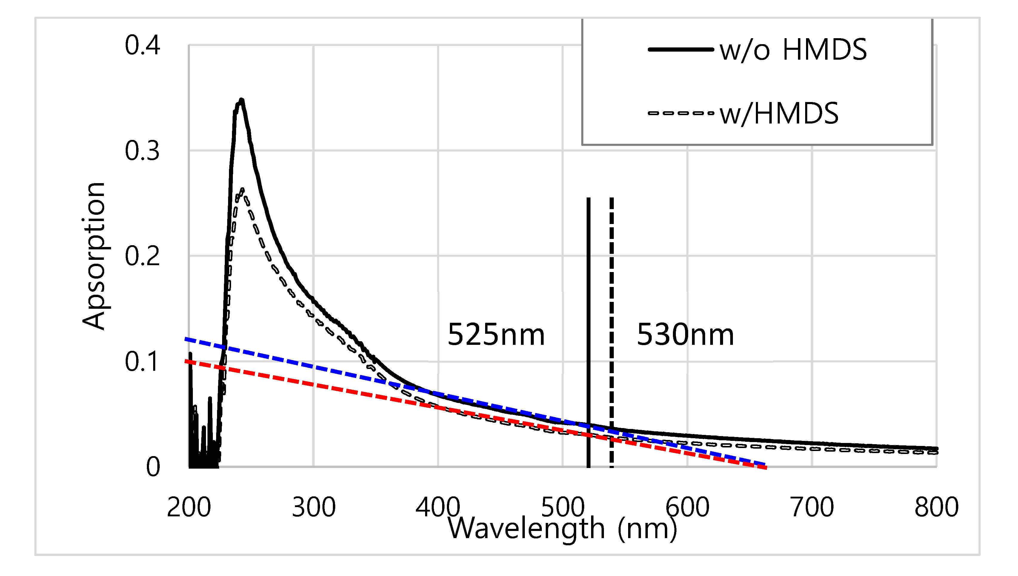
3.1. Introduction of HMDS for QD Improvement

For the first approach to improve the material properties of QDs itself, the following two steps proceeded. The first step is to coat the QDs with HMDS, and the second step is to expose the HMDS-coated QDs under atmospheric conditions. The result of this process is the growth of the SiOx on the surface of QDs as shown in Figure 1a. HMDS is widely used in cleaning processes that oxidize around impurities on the semiconductor wafer surface with chemical stability and then remove them through etch [22,23]. With this in mind, it is intended to improve the properties by oxidation on the surface of QDs. In this work, we further expect the additional benefits from this simple process such that the thickness growth of the SiOx is self-limited and effectively passivate the defects located on the surface of QDs without deteriorating the intrinsic properties including the color-purity of QDs as we will discuss later in this work. For instance, the SiO(CH3)3 layer is known to be formed via the substitution reaction between ammonium in the HMDS chemicals and oxygen in the air as shown in Figure 1a. The growth of the SiO(CH3)3 layer on the CdSe/ZnS core-shell QDs surface is a self-limited process. Figure 1b represents the data of the high resolution-transmission electron microscopy (HR-TEM) measurement, and clearly shows the lattice of CdSe/ZnS core-shell QDs regardless of the coating with (W) and without (W/O) HMDS. It is, however, difficult to distinguish the existence of the nonstoichiometric oxide layer (i.e., SiOx) from the samples treated with HMDS in Figure 1b. We, in fact, expected this result because the Si–O–(CH3)3 layer can be formed only when the HMDS chemicals and oxygen in the air were simultaneously supplied.
Once the SiO(CH3)3 layer was formed on the CdSe/ZnS core-shell QDs surface, the substitution reaction between ammonium in the HMDS chemicals and oxygen in the air was limited. The growth of SiO(CH3)3 layer with consequently the SiO bonds on the surface of the CdSe/ZnS core-shell QDs is the self-limited process, causing the non-distinguishable HR-TEM results in Figure 1b. Another method of determining the presence of the SiO(CH3)3 layer (i.e., SiO bonds) is to determine the presence of oxygen and silicon on the QD surface using the EDX component mapping method. Regardless of coating the CdSe/ZnS QDs with HMDS, the elements of Cd, Se, Zn, and S were clearly observed in the EDX results shown in Figure 1c as expected. The element of Si, however, demonstrates the roles of the HMDS coating: the samples coated with HMDS show the Si pattern of evenly dispersed QDs. It is, however, practically impossible to distinguish the form of QDs in the case of the samples measured without the HMDS treatment. It is also interesting to notice that the HMDS-coated QDs were well dispersed because the hydrophobic interface was created by the CH3 groups in the SiO(CH3)3 layer. The degree of dispersion can be checked from the atomic force microscope (AFM) results in Figure A1 in the Appendix A. It can be seen that the roughness of QD coated using HMDS is excellent. Oxygen element is always present in the air, making it difficult to distinguish using the EDX component mapping method. The Si and O elements on the CdSe/ZnS QD surface were additionally investigated by the XPS measurement technique as shown in Figure 1d. The intensities of both O 1s and Si 2p are higher when the CdSe/ZnS QDs were coated with HMDS, indicating the formation of the SiO bonds on the CdSe/ZnS QD surface. The strong intensity in XPS means that the number of bonds of the element corresponding to the energy is large. When the QD was blended with HMDS, the intensity of O increased, indicating that the number of bonds of oxygen increased and it became oxidation. Furthermore, for the samples treated with HMDS, the peak position of the O 1s signal shifted toward the direction of higher binding energy. This observation also suggests that the samples treated with HMDS move to a higher oxidation state due to the formation of SiO(CH3)3 on the CdSe/ZnS QD surface. In [24], it is said that the oxygen bound to the organic component increases the binding energy range from 530.9 to 533.8 eV. When HMDS was not coated on QD, O 1s was 531.7 eV, and when HMDS was coated, O 1s showed a peak of 533.3 eV. It was found that the binding energy was increased by 533.3 eV as carbon, the organic component, was combined with O. It can be predicted from the increased binding energy that Si–O–(CH3)3 is formed. As described above, despite the fact that the Oxide layer was not visible at the QD edge from the TEM results, the Si component was confirmed in EDX, and the presence of oxygen was predicted by the strong intensity and the increased binding energy of O 1s in XPS. From these results, rather than a uniform oxide layer, it is considered that a thin oxide of the extent to passivation of defects of QDs in various places is formed. Further analysis of the passivated material on the surface of the CdSe/ZnS QD is necessary for future analysis.

3.2. The Roles of HMDS Coating of the QD on the Improvement of QD-LED Characteristics

To clarify the effects of the HMDS-coated QDs on the electrical and optical characteristics of the QD-LEDs, we prepared the test samples without the glass capping layer (i.e., no encapsulation) as shown in Figure 2a. Patterned indium tin oxide (ITO) and aluminum (Al) were used as the anode and the cathode, respectively. The functions of poly(ethylenedioxythiophene): polystyrene sulphonate (PEDOT:PSS), poly(9-vinylcarbazole) (PVK) and ZnO are the hole injection layer (HIL), the hole transport layer (HTL), and the electron transport layer (ETL), respectively. Additionally, they were all spin-coated to make the multi-layered structure.
All manufacturing processes were carefully performed under a controlled environment in the N2 glove box to avoid the unwanted contamination or oxidation of QD-LEDs except for HIL PEDOT:PSS coating. The hole mobility of PVK employed as HTL is known to be 2.5 × 10⁻⁶ cm2 V−1 s−1 [4]. On the other hand, the mobility of electron in ETL of ZnO is known to be 1.8 × 10⁻³ cm2 V−1 s−1 [17], which is approximately 1000 times faster than the hole mobility in PVK. This significant discrepancy in mobility can cause the problem of charge imbalance in QD-LEDs: we attempted to find the solution for this type of problem via the emission profiling study and describe it later in this paper. Figure 2b demonstrates the energy levels of QD-LED shown in Figure 2a. In PVK, the highest occupied molecular orbital (HOMO) and the lowest unoccupied molecular orbital (LUMO) are 5.5 and 2.0 eV, respectively. In contrast, the HOMO and the LUMO energy level for ZnO are 7.5 and 4.2 eV, respectively. In this scheme, an energy barrier for electron injection from the cathode (i.e., Al electrode) to the ETL layer of ZnO with the LUMO level of 4.2 eV is small enough, and therefore electrons can easily reach to CdSe/ZnS QDs. Now, electrons can be confined within CdSe/ZnS QDs since PVK provides a high enough energy barrier to block the injection of electrons to ITO. The efficiency of hole injection from ITO to CdSe/ZnS QDs is high since the energy barrier between the HOMO of PEDOT:PSS and PVK is small enough for hole injection, although a relatively high energy band offset exists between PVK and CdSe/ZnS QDs. The energy level for CdSe/ZnS QDs can effectively confine the charges (i.e., injected electrons and holes) within the QD emitting layer, resulting in the efficiency improvement of charge recombination. Data shown in Figure 2c–f show the effects of an HMDS treatment of QD-LEDs on the reliability, J-V characteristics, luminance, and efficiency, respectively. Note that the test samples used for these measurements were fabricated without the glass capping layer to monitor the roles of the HMDS treatment as quickly as possible. Results in Figure 2c illustrate the initial stage of luminance degradation with time: the change in luminance characteristics of QD-LED samples was investigated as a function of time while applying a constant current that set to obtain the initial luminance (L0) of 1000 cd/m2. The test samples with HMDS-coated quantum dots (i.e., denoted by HMDS1 and HMDS2) exhibits a significant improvement in reliability. For instance, the luminance more rapidly degrades below 50% of the initial value with the stress time in the QD-LED samples without the additional HMDS coating process (i.e., denoted by Ref1 and Ref2). We suggest that this significant luminance improvement by the simple HMDS treatment is the curing effect of surface defects of CdSe/ZnS QDs by the SiO(CH3)3. In Figure 2d–f, the test samples made of CdSe/ZnS QDs without the HMDS treatment are denoted as Ref, while HMDS1 and HMDS2 are the test samples processed by the different concentrations of HMDS (refer to Table 1). The data in Figure 2d,e indicate that the simple HMDS treatment of CdSe/ZnS QDs improves the property of luminance even though the current density is low as compared to the one of Ref. This result indicates that current loss via a Joule heat consumption was reduced by the simple HMDS treatment so that current effectively converted into light. Consequently, the efficiency of both HMDS1 and HMDS2 is higher than that of Ref in Figure 2f. As listed in Table 1, the simple HMDS treatment of QDs increased the maximum efficiency of test samples up to 1.7 and 1.8 times for HMDS-1 and HMDS-2, respectively. We believe that the deactivation of surface defects on QDs by the SiO(CH3)3 improves the amount of photon conversion. Additionally, based on the same reason, we observed the improvement of the maximum luminance up to 15–18%. The results of the reproducibility experiment are summarized in Table A2 of Appendix A, and the distribution of luminance values was not large depending on the conditions.

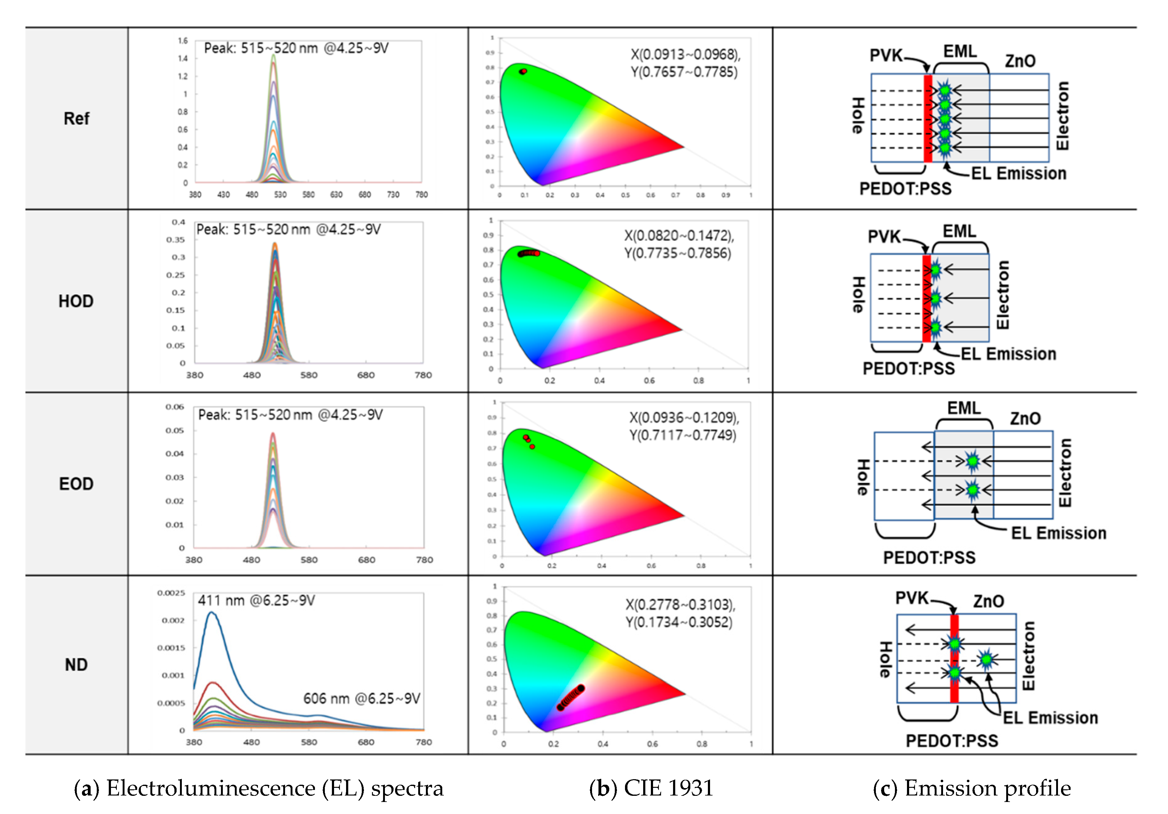
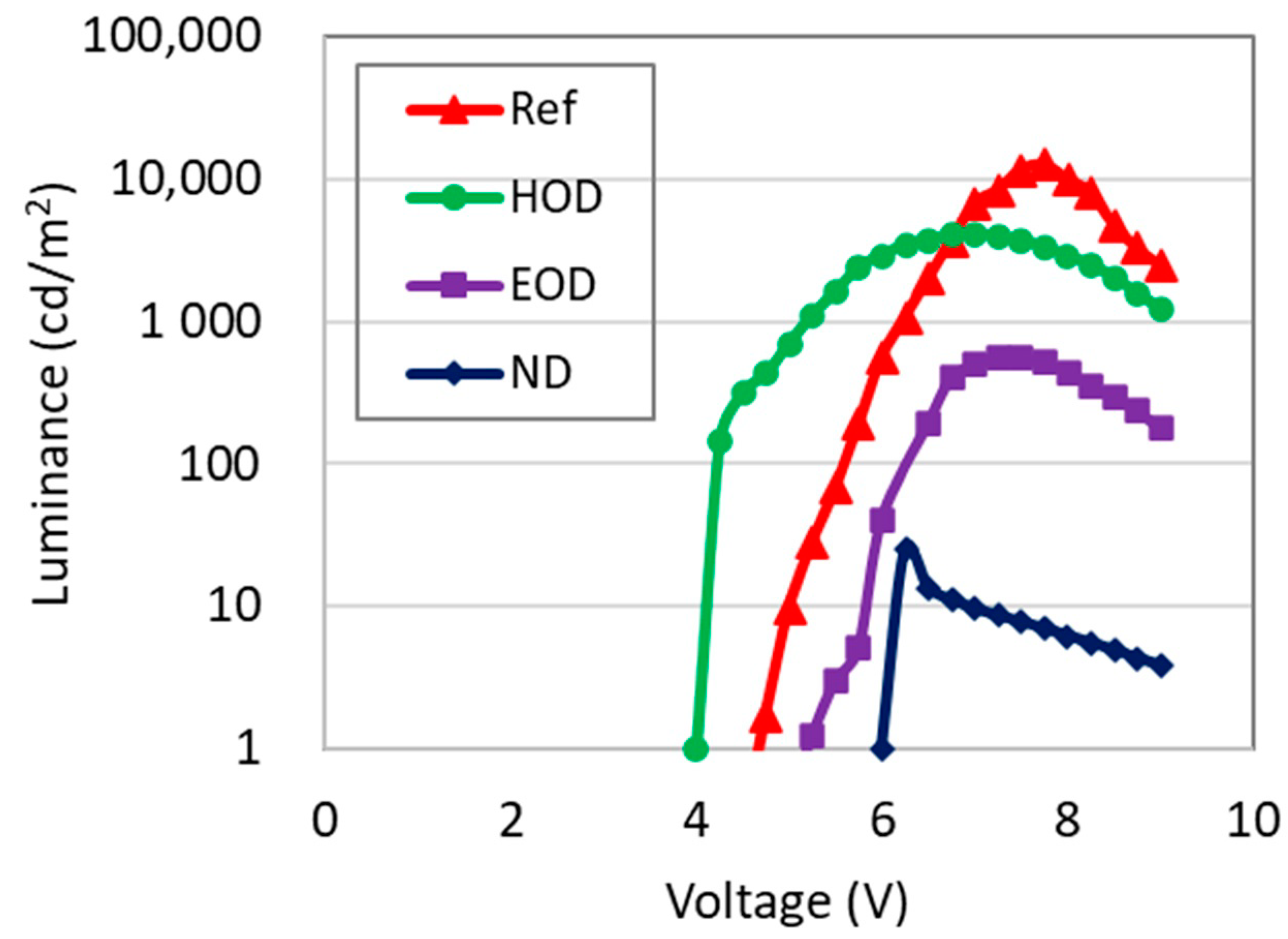
3.3. The Emission Profiling Study for Characterizing the Flow of Charge

By adding the HMDS coating step for minimizing the surface defects on QDs to the conventional fabrication process, we obtained the substantial improvement of QD-LED characteristics as discussed above. In addition to improving the QD properties themselves, we conducted the emission profiling study using the various types of devices (e.g., hole only device, electron only device, etc.) to understand how electrons and holes flow through the layers. Based on the data obtained from the emission profiling study, we can research how to improve current efficiency by achieving charge balance through the structural adjustment of QD-LEDs. We prepared various types of test samples for this purpose: for instance, in Figure 3, “reference (Ref)” represents the QD-LED device with the HMDS treatment process, “hole only device (HOD)” is the HMDS-treated QD-LED device without a ZnO ETL layer, “electron only device (EOD)” is the HMDS-treated QD-LED device without a PVK HTL layer, and finally “no-QD device (ND)” represents the test samples without the HMDS-treated QDs.
Data shown in the first column and the second column in Figure 3 are the electroluminescence (EL) spectra and the Commission internationale de l’ éclairage (CIE) 1931 chart (CIE 1931) color space chromaticity diagram, respectively, of the test samples employed in this work for the emission profiling study. Based on the experimental results of the first two columns, we analyzed the emission profiles shown in the third column in Figure 3. Data shown in the first column in Figure 3 show the EL spectra of the various samples at the driving voltage from 4.25 to 9 V. All test devices except ND produced the EL spectra of 515–520 nm wavelength (i.e., green light emission). Nonetheless, the maximum luminance observed from the HOD and EOD samples was approximately 1/3 and 1/22, respectively, as compared to the one recorded from the Ref sample (refer to Table 2). The characteristics of ND were different from the other samples (i.e., Ref, HOD, and EOD): for instance, we observed the EL peaks with the wavelength of 410 nm (i.e., blue light emission), but the intensity was very weak. We also found a broad EL peak with the wavelength of 400~700 nm. The EL spectra of Ref, HOD, and EOD represent the same green light emission, suggesting that the exciton recombination occurred within EML. Regarding the case of Ref, we expect that the electron-hole recombination occurs mainly near the EML-PVK interface since the electron mobility in ZnO was 1000 times faster than the hole mobility in PVK. Furthermore, the energy difference between the LUMO level of PVK (2.0 eV) and the one of EML (4.3 eV) is big enough to block the electron injection into PVK. Consequently, PVK acts as an electron blocking layer (EBL), and therefore, the electrons accumulate near the EML-PVK interface, and start to emit as soon as the holes with relatively low mobility are finally transferred to EML. Regarding the case of HOD, the electron injected into EML directly from the cathode without assisting by ETL, resulting in the reduced electron injection. This phenomenon caused the decrease of EL intensity by three times. The emission occurs within EML regardless of the existence of ZnO in HOD because PVK still acts as EBL. In the case of EOD without PVK, we shall observe the charge-imbalance problem since the ZnO layer with high electron mobility effectively helps to inject the large number of electrons into EML. On the other hand, hole injection into EML decreases due to the lack of hole transfer from the anode without HTL. This charge-imbalance phenomenon reduced emission efficiency by 22 times as compared to the one of Ref. Additionally, we may expect the exciton formation does not strictly restrict within EML because of no PVK in EOD. As shown in the EL spectra, however, luminescence occurs mostly in EML, although the EL intensity is very weak. We interpret that both the fast electron mobility in ZnO and the low injection efficiency of the hole causes this observation. The majority of injected electrons that did not convert into light within EML then dissipated via a Joule heat consumption. In the case of ND, the light emission occurs at both ETL (i.e., the blue emission with the 410 nm wavelength in PVK) and HTL (i.e., the white emission with the 400–700 nm wavelength in ZnO) because we did not use QDs to make the samples. However, the intensities of all EL peaks were very weak, and especially the EL peak observed in the region of white wavelength of 400–700 nm was barely distinguishable. We anticipate that this phenomenon is due to the difference in carrier mobility between PVK and ZnO. The exciton recombination mainly occurred at the PVK region because the electron mobility in ZnO is faster than that of injected holes in PVK, indicating that the injected electrons from the cathode arrived at PVK very fast to recombine with the slowly moving holes.
Data in Figure 4 and Table 2 represent luminance as a function of voltage and the maximum luminance of the test samples, respectively. Based on the experimental results in Figure 4 and Table 2, the emission profiling study using the various types of devices (i.e., Ref, HOD, EOD, and ND) helps us to understand how electrons and holes flow through the layers. First, PVK used as HTL has more significant roles in the luminous efficiency than that of ZnO used as ETL: the values of maximum luminance of both EOD without PVK and HOD without ZnO reduced up to the 1/22 and the 1/3 of Ref, respectively. Second, in the test samples except ND, the recombination of injected electron and holes via an exciton formation occurs mainly in the EML region, but very near the EML-PVK interface since the electron mobility in ZnO is 1000 times faster than the hole mobility in PVK that also acts as EBL. For the high efficiency of luminance, therefore, we recommend controlling the centroid of electron-hole recombination. For example, if we can properly control the position of light emission to be located at the center of EML by selecting the thicknesses of PVK and ZnO, it is possible to minimize the problem caused by the charge imbalance and enhance the efficiency of luminance. The results of the reproducibility experiment are summarized in Table A3 of Appendix A, and the distribution of luminance values was not large depending on the conditions of each sample.

3.4. The Charge Balance Through the Thickness Adjustment of Both ETL and HTL

Data in Figure 5 and Table 3 represent the effects of thickness adjustment of PVK and ZnO by adjusting the time of a spin coating process. As compared to the values of Ref, the thickness of ZnO in Sample 1 increased to delay the electron transport by reducing the spin-coating time from 60 to 30 s. On the other hand, when the spin coating time for PVK was increased from 30 to 60 s, the thickness of the PVK layer became thinner, thereby reducing the hole transport time from HTL to EML. Even though Sample 3 had the same thickness conditions as Sample 2, it did not blend QD and HMDS, resulting in low luminance and efficiency. The effectiveness of HMDS was again confirmed. Data in Figure 5a indicate that all four samples have both the similar EL peaks at the wavelength of 523–529 nm and the sharp emission spectra (e.g., FWHM of 22 nm). To measure the bandgap of QD, a Ultraviolet-visible (UV) spectrometry technique was used, and the wavelength from the absorption spectra in Figure A2 of the Appendix A was identified as 525 ~ 530nm, and the calculated bandgap value was 2.3~2.4 eV. The frequency and bandgap energy of the absorption spectrum of QD with or without HMDS are summarized in Table A1.
The inset shows green emission light observed in dark chamber with power supply and spectroradiometer and is also confirmed by the CIE 1931 chart in Figure 5b. As we expected, Sample 2 with both a thinner PVK and a thicker ZnO results in the highest EL intensity peak since the problem of charge imbalance was minimized as compared to the one of Ref. Additionally, it is interesting to note that the EL intensity of Sample 1 is higher than Ref but lower than Sample 2: the thickness of ZnO in Sample 1 was thicker than that of Ref so that we intentionally obtained the time delay for the electron transport to EML. However, the thicknesses of PVK in both Ref and Sample 1 were the same, suggesting that the difference in the EL intensity between Sample 1 and Sample 2 is due to the thickness difference of PVK. HTL and ETL of Sample 2 and Sample 3 have the same thickness, but QD without HMDS was used for Sample 3. Electroluminescence in Figure 5c is consistent with experimental results of Figure 5a,b. Figure 5d,f shows the experimental results of current density, luminance, and efficiency, respectively. Data in Figure 5d suggest that turn-on voltage (Von) can be optimized by properly selecting the thicknesses of PVK and ZnO. As compared to the measured Von of Ref, a significant reduction of Von (i.e., from 5.5 to 5.0 V) was observed in Samples 1 and 2. It is interesting to note that the value of Von is more sensitive to the thickness change of PVK and ZnO. We speculate that this phenomenon is due to the degree of charge-imbalance improvement. As shown in Figure 5e,f, as compared to Ref, luminance was improved by 2.9 and 4.4 times for Sample 1 and Sample 2, respectively. Additionally, efficiency that was converted from the data listed in Figure 5d,e was increased by 2.5 and 2.7 times for Samples 1 and 2, respectively. In addition, from the results of Samples 2 and 3, it was found that when QD and HMDS were not blended, luminance and efficiency were poor under the same HTL and ETL thickness conditions. Although the properties such as Von, luminance, and efficiency of QD-LEDs were improved by properly adjusting the thicknesses of PVK and ZnO, the emission center for the EL spectra was hardly changed as shown in Figure 5a,b. This result suggests that we can improve the EL characteristics without any side effects (e.g., unexpected color change) via the emission profiling study regardless of the QD-LED types. Until now, the highest luminance among Green CdSe/ZnS QDs is known as 614,000 cd/m2 published by Shen et al. [25]. Our research also seems to require further structural optimization.

4. Conclusions

In conclusion, we presented a unique fabrication method of highly efficient and charge-balanced QD-LEDs. First, to improve the property of materials itself, we effectively covered the surface of CdSe/ZnS core-shell quantum dots with the SiO(CH3)3 by simply mixing QDs with HMDS under atmospheric conditions. Based on the experimental data (e.g., HR-TEM, EDX, and XPS), we estimated that the growth of the SiO(CH3)3 on the surface of QDs is self-limited: the SiO(CH3)3 then effectively passivate the defects located on the surface of QDs without deteriorating the intrinsic properties including the color-purity of QDs. By simply employing this process to the conventional QD-LED fabrication step, we observed the substantial improvement of device characteristics such that the current efficiency, the maximum luminance, and the QD lifetime were improved by 1.7–1.8 times, 15–18%, and nine times, respectively. Second, to enhance the emission efficiency at QDs, we performed the emission profiling study using the different types of test devices (e.g., HOD, EOD, etc.) to understand how electrons and holes flow through layers consisting of the newly proposed QD-LEDs with the HMDS treatment process. Based on the experimental results of the emission profiling investigation, we found that it is recommended to reduce the thickness of HTL (e.g., PVK in this work) and to increase the thickness of ETL (e.g., ZnO in this work) in order to make the charge balance, so that to improve both the maximum luminance and the current efficiency of QD-LEDs. Our simple and novel fabrication methodology in this work (i.e., HMDS coating of QDs and optimization of charge balance) will be a catalyzer that can trigger cost effective productions and reliable QD-LED fabrication with respect to design and application for next generation display and technologies.

Author Contributions

This paper was accomplished based on the co-work of the authors. J.P. (Junekyun Park) carried out experiments, analyzed data, interpreted the results of experiments, and wrote the paper. E.S. contributed to analyzing data and interpreting experimental results. J.P. (Jongwoo Park) contributed to experimental design. Y.R. supervised the entire research progress. All authors have read and agreed to the published version of the manuscript.

Funding

This research was supported by Basic Science Research Program through the National Research Foundation of Korea (NRF) funded by the Ministry of Education (NRF-2018R1D1A1B07047719).

Conflicts of Interest

The authors declare no conflict of interest.

Appendix A

Coating HMDS on QD forms the Si–O–(CH3)3 bond that includes the carbon group of CH3. In general, it is well known that the carbon groups (CH, CH2, CH3) are nonpolar and hydrophobic. Therefore, we expect that the SiO(CH3)3 bonds formed on the surface of QDs force QDs to distribute uniformly as we discussed in Figure 1c and as shown in Figure A1.
Figure A1. Atomic force microscope (AFM) images show the roughness of the electron transport layer (EML) layer without (a) and with (b) the HMDS treatment. A comparison of the root mean square (RMS) values indicates the HMDS treatment of QDs results in the smooth surface morphology in addition to the uniform distribution of QDs.
Applsci 10 06081 g0a1
CdSe/ZnS QDs used in this work emitted the green light as shown in Figure 1d, Figure 3 and Figure 5. The bandgaps of CdSe/ZnS QDs were measured using the UV-visible spectrometry technique. Based on the UV-visible absorption spectra in Figure A2, the wavelength of CdSe/ZnS QDs was in the range of 525–530 nm. Additionally, this result is well consistent with the electroluminescence result shown in Figure 5, and the calculated bandgap values in Table A1 are in the range of 2.3–2.4 eV.
Figure A2. Bandgap measurement of QDs using UV-visible spectrometry.
Applsci 10 06081 g0a2
Table A1. Wavelength and bandgap energy of QDs without and with HMDS.
ItemW/O HMDSW HMDS
Wavelength (nm)525530
Bandgap energy (eV)2.362.34
The band gap was calculated from the wavelength value at which the abrupt change in absorbance occurs. E = hc/wavelength. The band gaps w/o and with HMDS were 1240/525 = 2.36 eV and 1240/530 = 2.34 eV, respectively. Where h is the Frank’s constant, c is the speed of light. Therefore, hc = 1240.
The reproducibility experiment for voltage-luminance in Figure 2 and Table 1 was conducted and the results are as follows. The distribution of luminance according to conditions was not large.
Table A2. The maximum luminance and efficiency for each condition. (Measurement of four devices from two samples.)
ItemSample No.12Average
Device No.1212
Max. LuminanceRef99729835993710,1359970
HMDS-111,53811,36211,64911,73611,571
HMDS-211,78311,57211,62311,81411,698
Max. EfficiencyRef7.07.27.37.47.2
HMDS-112.112.312.412.512.3
HMDS-212.812.612.512.612.9
The reproducibility experiment for voltage-luminance in Figure 4 and Table 2 was conducted and the results are as follows. The distribution of luminance according to conditions was not large.
Table A3. The maximum luminance for each condition. (Measurement of six devices from two samples.)
Sample No.Sample 1Sample 2Average
Device No.123123
Ref12,48812,43211,45312,71111,65012,66012,232
HOD4074437240954556430848594377
EOD562476559776832409602
ND25262317151821

References

  1. Mitschke, U.; Bäuerle, P.J. The electroluminescence of organic materials. Mater. Chem. 2000, 10, 1471–1507. [Google Scholar] [CrossRef]
  2. D’Andrade, B.W.; Thompson, M.E.; Forrest, S.R. Controlling Exciton Diffusion in Multilayer White Phosphorescent Organic Light Emitting Devices. Adv. Mater. 2002, 14, 147–151. [Google Scholar] [CrossRef]
  3. Nayak, P.K.; Agarwal, N.; Ali, F.; Patankar, M.P.; Periasamy, N.J. Blue and white light electroluminescence in a multilayer OLED using a new aluminium complex. Chem. Sci. 2010, 122, 847–855. [Google Scholar] [CrossRef] [Green Version]
  4. Lee, D.; Liu, Y.; Lee, K.; Chae, H.; Cho, S.M. Effect of hole transporting materials in phosphorescent white polymer light-emitting diodes. Org. Electron. 2010, 11, 427–433. [Google Scholar] [CrossRef]
  5. Caruge, J.-M.; Halpert, J.E.; Bulovic, V.; Bawendi, M.G. NiO as an Inorganic Hole-Transporting Layer in Quantum-Dot Light-Emitting Devices. Nano Lett. 2006, 6, 2991–2994. [Google Scholar] [CrossRef]
  6. Park, S.; Yun, W.M.; Kim, L.H.; Park, S.; Kim, S.H.; Park, C.E. Inorganic/organic multilayer passivation incorporating alternating stacks of organic/inorganic multilayers for long-term air-stable organic light-emitting diodes. Org. Electron. 2013, 14, 3385–3391. [Google Scholar] [CrossRef]
  7. Friend, R.H.; Gymer, R.W.; Holmes, A.B.; Burroughes, J.H.; Marks, R.N.; Taliani, C.; Bradley, D.D.C.; Santos, D.A.D.; Bredas, J.L.; Logdlund, M.; et al. Electroluminescence in conjugated polymers. Nature 1999, 397, 121–128. [Google Scholar] [CrossRef]
  8. Chen, J.; Zhao, D.; Li, C.; Xu, F.; Lei, W.; Sun, L.; Nathan, A.; Sun, X.W. All Solution-processed Stable White Quantum Dot Light-emitting Diodes with Hybrid ZnO@TiO2 as Blue Emitters. Sci. Rep. 2014, 4, 4085. [Google Scholar] [CrossRef] [Green Version]
  9. Jiang, X.; Liu, S.; Liu, M.S.; Ma, H.; Jen, A.K.-Y. Organic light-emitting diodes using an in situ thermally polymerized hole transporting layer. Appl. Phys. Lett. 2000, 76, 2985–2987. [Google Scholar] [CrossRef]
  10. Zhao, J.; Bardecker, J.A.; Munro, A.M.; Liu, M.S.; Niu, Y.; Ding, I.-K.; Luo, J.; Chen, B.; Jen, A.K.-Y.; Ginger, D.S. Efficient CdSe/CdS Quantum Dot Light-Emitting Diodes Using a Thermally Polymerized Hole Transport Layer. Nano Lett. 2006, 6, 463–467. [Google Scholar] [CrossRef]
  11. Caruge, J.M.; Halpert, J.E.; Wood, V.; Bulovic, V.; Bawendi, M.G. Colloidal quantum-dot light-emitting diodes with metal-oxide charge transport layers. Nat. Photonics 2008, 2, 247–250. [Google Scholar] [CrossRef]
  12. Cho, K.-S.; Lee, E.K.; Joo, W.J.; Jang, E.; Kim, T.-H.; Lee, S.J.; Kwon, S.-J.; Han, J.Y.; Kim, B.-K.; Choi, B.L.; et al. High-performance crosslinked colloidal quantum-dot light-emitting diodes. Nat. Photonics 2009, 3, 341. [Google Scholar] [CrossRef]
  13. Qian, L.; Zheng, Y.; Xue, J.; Holloway, P.H. Stable and efficient quantum-dot light-emitting diodes based on solution-processed multilayer structures. Nat. Photonics 2011, 5, 543. [Google Scholar] [CrossRef]
  14. Kwak, J.; Bae, W.K.; Lee, D.; Park, I.; Lim, J.; Park, M.; Cho, H.; Woo, H.; Yoon, D.Y.; Char, K.; et al. Bright and Efficient Full-Color Colloidal Quantum Dot Light-Emitting Diodes Using an Inverted Device Structure. Nano Lett. 2012, 12, 2362–2366. [Google Scholar] [CrossRef]
  15. Mashford, B.S.; Stevenson, M.; Popovic, Z.; Hamilton, C.; Zhou, Z.; Breen, C.; Steckel, J.; Bulovic, V.; Bawendi, M.; Coe-Sullivan, S.; et al. High-efficiency quantum-dot light-emitting devices with enhanced charge injection. Nat. Photonics 2013, 7, 407. [Google Scholar] [CrossRef]
  16. Bae, W.K.; Park, Y.-S.; Lim, J.; Lee, D.; Padilha, L.A.; McDaniel, H.; Robel, I.; Lee, C.; Pietryga, J.M.; Klimov, V.I. Controlling the influence of Auger recombination on the performance of quantum-dot light-emitting diodes. Nat. Commun. 2013, 4, 2661. [Google Scholar] [CrossRef] [PubMed] [Green Version]
  17. Dai, X.; Zhang, Z.; Jin, Y.; Niu, Y.; Cao, H.; Liang, X.; Chen, L.; Wang, J.; Peng, X. Solution-processed, high-performance light-emitting diodes based on quantum dots. Nature 2014, 515, 96. [Google Scholar] [CrossRef] [PubMed]
  18. Kim, D.; Fu, Y.; Kim, S.; Lee, W.; Lee, K.-H.; Chung, H.K.; Lee, H.-J.; Yang, H.; Chae, H. Polyethylenimine Ethoxylated-Mediated All-Solution-Processed High-Performance Flexible Inverted Quantum Dot-Light-Emitting Device. ACS Nano 2017, 11, 1982–1990. [Google Scholar] [CrossRef]
  19. Cao, S.; Zheng, J.; Zhao, J.; Yang, Z.; Li, C.; Guan, X.; Yang, W.; Shang, M.; Wu, T. Enhancing the Performance of Quantum Dot Light-Emitting Diodes Using Room-Temperature-Processed Ga-Doped ZnO Nanoparticles as the Electron Transport Layer. ACS Appl. Mater. Interfaces 2017, 9, 15605–15614. [Google Scholar] [CrossRef] [Green Version]
  20. Sun, Y.; Wang, W.; Zhang, H.; Su, Q.; Wei, J.; Liu, P.; Chen, S.; Zhang, S. High-Performance Quantum Dot Light-Emitting Diodes Based on Al-Doped ZnO Nanoparticles Electron Transport Layer. ACS Appl. Mater. Interfaces 2018, 10, 18902–18909. [Google Scholar] [CrossRef]
  21. Zhang, Z.; Ye, Y.; Pu, C.; Deng, Y.; Dai, X.; Chen, X.; Chen, D.; Zheng, X.; Gao, Y.; Fang, W.; et al. High-Performance, Solution-Processed, and Insulating-Layer-Free Light-Emitting Diodes Based on Colloidal Quantum Dots. Adv. Mater. 2018, 30, 1801387. [Google Scholar] [CrossRef] [PubMed]
  22. Xu, Y.; Fan, W.H.; Li, Z.H.; Wu, D.; Sun, Y.H. Antireflective silica thin films with super water repellence via a solgel process. Appl. Opt. 2003, 42, 108–112. [Google Scholar] [CrossRef] [PubMed]
  23. Fan, C.; Lin, Y.; Huang, C. Over 40 cd/A Efficient Green Quantum Dot Electroluminescent Device Comprising Uniquely Large-Sized Quantum Dots. Semicond. Sci. Technol. 2011, 26, 045006. [Google Scholar] [CrossRef]
  24. Beamson, G. High resolution XPS of organic polymers: The Scienta ESCA 300 Database; Wiley: Chichester, UK, 1992; p. 295. [Google Scholar]
  25. Shen, H.; Gao, Q.; Zhang, Y.; Lin, Y.; Lin, Q.; Li, Z.; Wang, S. Visible quantum dot light-emitting diodes with simultaneous high brightness and efficiency. Nat. Photonics 2019, 13, 192–197. [Google Scholar] [CrossRef]
Figure 1. Improvement of the quantum dot light emitting diodes (QD-LED) characteristics by adding a simple step to the conventional fabrication process: (a) a schematic for the surface reaction of the quantum dot (QDs) with hexamethyldisilazane (HMDS) and the formation of SiO bond as a consequence, (b) high resolution-transmission electron microscopy (HR-TEM) results for both without (W/O) and with (W) an HMDS treatment process. No clear evidence for the formation of the SiO bonds both in W/O HMDS (left) and in W HMDS (right) samples. (c) colored energy dispersive X-ray spectroscopy (EDX) results for both without (W/O) and with (W) the HMDS treatment process. Note the clear shape of Si elements only in W HMDS (right) samples. (d) X-ray photoelectron spectroscopy (XPS) results of O 1s and Si 2p obtained from the samples without (W/O) and with (W) an HMDS treatment process.
Applsci 10 06081 g001aApplsci 10 06081 g001b
Figure 2. The roles of HMDS coating of the CdSe/ZnS core-shell quantum dot on the improvement of QD-LED characteristics. To quickly confirm the effects of HMDS coating, we tested the QD-LEDs without the glass capping layer for the optical and electrical characterizations. (a) A schematic of QD-LED with newly proposed HMDS-coated the CdSe/ZnS core-shell quantum dot. (b) The energy levels of QD-LED and the effects of the HMDS treatment of QD-LEDs on (c) the reliability, (d) J-V characteristics, (e) luminance, and (f) efficiency. Where, Ref means QD-LED without HMDS, HMDS1 and HMDS2 mean QD-LEDs blended with HMDS.
Applsci 10 06081 g002
Figure 3. A step for the emission profiling study for characterizing the charge flow through the layers consisting of the newly proposed QD-LEDs: the first, second, and third columns represent the Electroluminescence (EL) spectra, the Commission internationale de l’ éclairage (CIE) 1931 chart, and the emission profile, respectively, for the various test samples. (a) is the measurement of the electroluminescence according to the voltage, and the emission color can be predicted from the peak value. (b) is a diagram that defines the wavelength distribution of the electromagnetic visible spectrum and the color perceived physiologically in human color vision. (c) shows the position where electrons and holes from the electrode move to the emission layer to form electron hole pairs and emit light through recombination. Ref, HOD, EOD, and ND are the abbreviations for the reference devices, the hole only devices, the electron only devices, and the devices without QDs, respectively. Note that the structure of HOD was the same as Ref except the ZnO layer that acts as both ETL and HBL. On the other hand, the structure of EOD was the same as Ref except the PVK layer that acts as both HTL and EBL. Using these schemes, we can study the roles of PVK and ZnO in the emission profile via the exciton formation. Where, Ref, HOD, EOD, and ND are the abbreviations for reference, hole only device, electron only device, and no-QD device, respectively.
Applsci 10 06081 g003
Figure 4. Luminance for the test devices employed for the emission profiling study.
Applsci 10 06081 g004
Figure 5. The effects of thickness change of both PVK and ZnO: (a) the EL spectra, (b) CIE 1931 chart, (c) electroluminescence, (d) current density as a function of the driving voltage, (e) luminance, and (f) efficiency. The EL spectra showed a wavelength of 523–529 nm regardless of the sample, and it was found that it was in a similar position on the CIE 1931 diagram. When power is applied to the metal terminal, it can be seen that the green color has a wavelength of 520–530 nm from the electroluminescence. We designed this experiment to find the optimal thickness combination for minimizing the problems caused by the charge imbalance phenomenon. The efficiency was obtained by dividing the luminance by the current density, and was best when the PVK thickness was thin and the ZnO thickness was increased.
Applsci 10 06081 g005
Table 1. The effects of the hexamethyldisilazane (HMDS) treatment on the characteristics of quantum dot light emitting diodes (QD-LEDs). Note that the ratio of HMDS-1 to of quantum dot (QD) was 1/10 and the ratio of HMDS-2 to QD was 4/10.
Turn-On Voltage (V)Maximum Luminance (cd/m2)Maximum Efficiency (cd/A)
Ref
(no HMDS treatment)
4.399727.0
HMDS-1
(QD = 10 mL and HMDS = 1 mL)
5.511,53812.1
HMDS-2
(QD = 10 mL and HMDS = 4 mL)
5.511,78312.8
Table 2. The maximum luminance for four devices.
Unit (cd/m2)Max. Luminance
Reference (Ref)12,488
Hole only device (HOD)4074
Electron only device (EOD)562
No-QD device (ND)25
Table 3. The effects of thickness change of both Poly 9-vinylcarbazole (PVK) and ZnO on current density, luminance, and efficiency. The best results were obtained from Sample 2 although the measured current density was the lowest one. QD without HMDS was used for Sample 3.
ItemSpin-Coating Conditions (s)Turn-On Voltage (V)Luminance
(cd/m2)
Efficiency
(cd/A)
RefPVK(30) and ZnO(60)5.512,00511.9
Sample 1PVK(30) and ZnO(30)5.035,27029.8
Sample 2PVK(60) and ZnO(30)5.053,12532.4
Sample 3PVK(60) and ZnO(30)5.041,17921.2

