Article

Real-Time Controller Design Test Bench for High-Voltage Direct Current Modular Multilevel Converters

1
Department of Electrical Engineering, Sukkur IBA University, Sukkur 65200, Pakistan
2
School of Electrical and Electronics Engineering, Chung-Ang University, Seoul 06910, Korea
*
Author to whom correspondence should be addressed.
Appl. Sci. 2020, 10(17), 6004; https://doi.org/10.3390/app10176004
Submission received: 30 July 2020 / Revised: 18 August 2020 / Accepted: 26 August 2020 / Published: 29 August 2020
(This article belongs to the Section Electrical, Electronics and Communications Engineering)

Abstract

:
Modular multilevel converters (MMCs), with their inherent features and advantages over other conventional converters, have gained popularity and remain an ongoing topic of research. Many scholars have solved issues related to the operation, control, protection, and reliability of MMCs using simulation software and small hardware prototypes. We propose a novel approach for an MMC controller design with real-time systems. By utilizing a key benefit of LabVIEW Multisim co-simulation, an MMC control algorithm that can be deployed on a field-programmable gate array (FPGA) was developed in LabVIEW. The complete circuit was designed in Multisim, and a co-simulation was performed to drive an MMC model. The benefit of this topology is that control algorithms can be designed in a LabVIEW FPGA and tested with the Multisim co-simulation circuit to obtain simulation results. Once the controller works and provides satisfactory results, the same algorithm can be deployed in any NI (National Instruments) FPGA-based controller, like a compact remote input/output (RIO), to control real-time MMCs designed in an NI PCI eXtensions for Instrumentation (PXI) system. This method saves time and provides flexibility for effectively designing control algorithms and implementing them in an FPGA for real-time model implementation.

1. Introduction

With increasing global warming, renewable energy sources are being used to generate power. Offshore wind turbines, because of the more linear wind velocity profile, are an example of a renewable energy source; however, they are located far away from load centers [1]. In transmitting power to load centers, high-voltage direct current (HVDC) transmission lines are preferred over high-voltage alternating current (HVAC) lines because they require fewer conductors and have less power losses, no skin effect, a reduced right of way, and good stability [2,3].
Modular multilevel converters (MMCs) are ideal converter topologies used for interfacing between HVDC and HVAC transmission systems. Compared with conventional converters, MMCs are more advantageous because they have modularity, scalability in terms of voltage and current, redundancy, good reliability, independent control of active and reactive power, low switching frequency, low total harmonic distortion (THD) in the output waveforms, and no filter requirement [4]. The first MMC HVDC was commissioned in December 2013 on Nan’ao Island, and another MMC HVDC system was installed on the Zhoushan Islands, China [5].
Many researchers are studying design control schemes for MMCs. For instance, the authors in [6] developed a simplified capacitor voltage balancing technique that does not require sorting to select submodules. In [7], the circulating currents of MMCs were controlled using an adaptive proportional integral (API) controller to reduce secondary harmonic components, and its performance was measured and compared with a proportional resonant (PR) controller for transient response, stability, optimal performance, and reference tracking in MATLAB. The authors in [8] proposed an energy-balancing control strategy to keep an MMC operating normally under submodule (SM) fault conditions in which PSCAD was used to simulate the system, and a small prototype was used to validate the results. A novel control strategy for MMCs based on differential flatness theory was proposed in [9]. Their results highlight the capability of the proposed controller in steady and dynamic conditions while maintaining MMC currents and voltages by controlling active and reactive power. Several researchers have developed small prototypes to verify their control algorithms. The algorithms are developed early in the simulation process and need to be written for the controller chosen to run the prototype, which takes time and effort and is costly [10,11,12,13,14,15,16,17,18,19,20,21]. As an emerging technology, there are few tools for MMC controller design and no established standards to guide engineering practices for MMC control and operation. Thus, there is a need for a platform where control algorithms are designed once and can be utilized for simulation and real-time implementation, ultimately saving time during the development and testing of the system.
This study presents a development platform using a LabVIEW Multisim co-simulation (Figure 1) that can develop control algorithms in a graphical-language-based LabVIEW platform for MMC simulation and allows the same program to be used for the control of the real-time MMC system implemented in a National Instruments (NI) PCI eXtensions for Instrumentation (PXI) system. In LabVIEW Multisim co-simulation, the control algorithm is designed with a LabVIEW field-programmable gate array (FPGA), and the circuit is developed in Multisim. Using the control algorithm, the circuit can be operated with the controls designed in LabVIEW. Therefore, the proposed real-time controller design test bench for HVDC MMCs saves time, money, and effort required for the development and testing of the system.

2. Comparison with Conventional Methods

Andrus et al. [22] studied a test bed design for HVDC systems to design fault management with a scaled-down MMC with a full bridge, but their system cannot be extended further due to hardware limitations. The work presented in [23] demonstrates a real-time simulation of an MMC-based MVDC traction system in which an FPGA-based system is used for real-time simulation. Additionally, a second offline simulation, PSCAD/EMTDC, was used for simulation and real-time verification of the results. The authors of [24] presented a 5 MW test bed hardware setup where the simulation results were verified from the test bed; however, the hardware was put at risk. In [25], a small prototype was developed with 10 SMs in each arm, and control algorithms were developed for a system with NI controllers. However, the system was limited to only 10 SMs, so the simulation results were obtained with different software. Several other studies [26,27,28] presented test beds for HVDC systems, but their systems either limited or lacked simulation verification without changing the control algorithm.

3. Operating Principles and Mathematical Modelling of the Proposed Controller Design Test Bench for the HVDC MMC

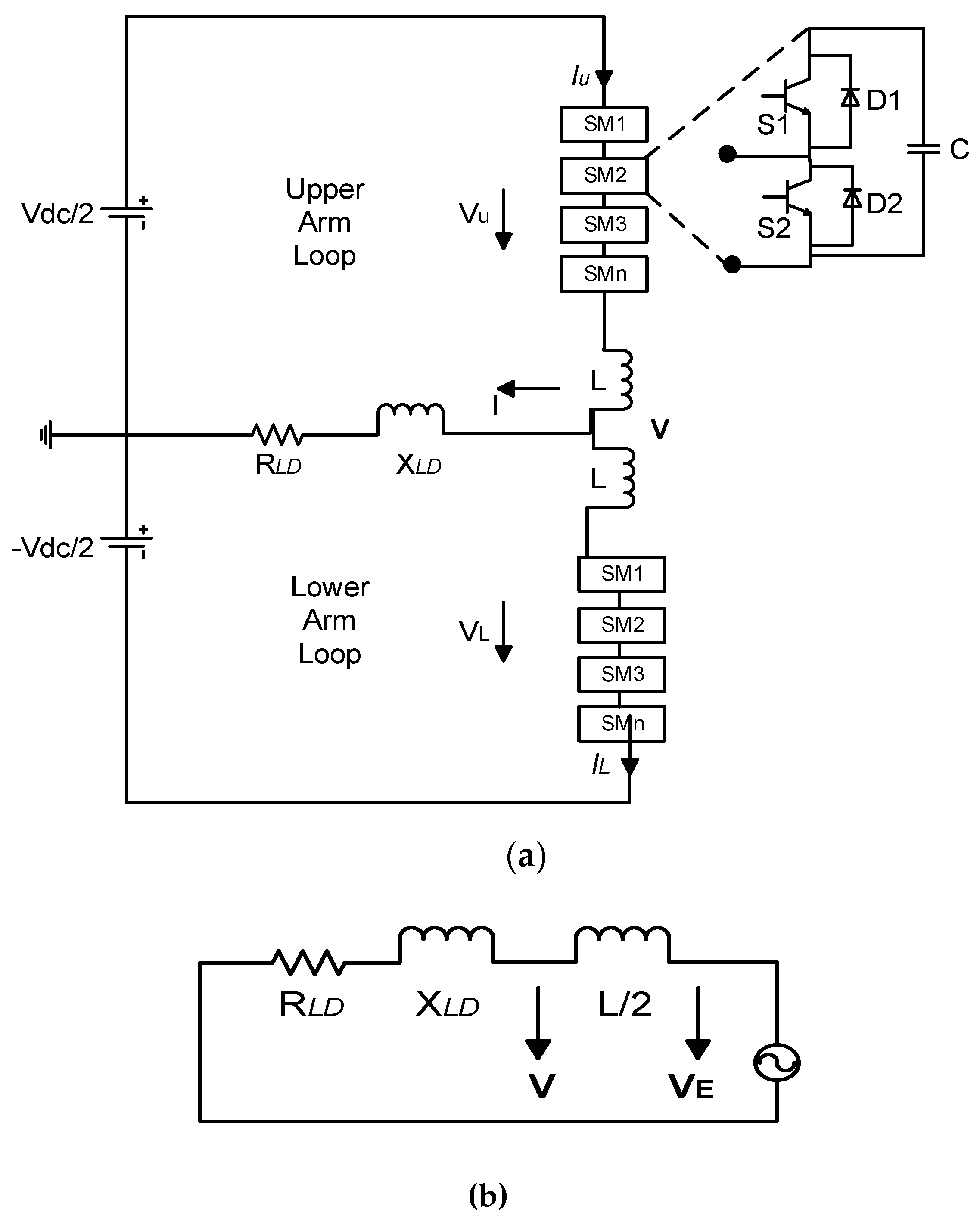
The single-phase topology of the MMC is shown in Figure 2a, which is composed of one phase/arm. The phase is further divided into an upper arm and a lower arm connected together by inductors. Each arm has N connected submodules (SMs) (SM1, SM2, etc.) in series, and each SM consists of two switches and a capacitor connected across them. By applying Kirchhoff’s voltage law (KVL) in the upper and lower loops, as shown in Figure 2a, we obtain
V = 1 2 V d c V u L d i U d t
V = 1 2 V d c + V L + L d i L d t
Then we apply Kirchhoff’s current law (KCL) to obtain the output current:
i = i L + i U
The equivalent circuit of the MMC is shown in Figure 2b. Using Equations (1) and (2), the output voltage is
V = 1 2 ( V L V U ) + L 2 d i d t
It is clear from Equation (3) that the equivalent inner voltage of the phase can be expressed as
V E = 1 2 ( V L V U )
Generally, the VE can be shown as
V E r e f = m V d c 2 cos ( ω t )
where m is the modulation index with 0 < m < 1 and ω is the angular frequency. N submodules are used in the circuit with conventional NLM methods, so Equation (7) is satisfied on the DC side.
V d c = V L + V U
Reference voltages for the upper and lower arms can be expressed as
V U r e f = V d c 2 [ 1 m cos ( ω t ) ]
V L r e f = V d c 2 [ 1 + m cos ( ω t ) ]
The circulating currents flowing due to the voltage difference in each arm can be found by Equations (10)–(12). These currents distort the leg current, produce additional heat in the switches, increase the rated current of power devices, and cause loss in the MMC. They must be controlled and reduced to avoid losses and reduce system cost.
i U = i c i r c + i 2
i L = i c i r c i 2
i c i r c = i U + i L 2
Equations (1) and (2) provide an understanding of the operation of the MMC. The SM voltages should be equal to ½ Vdc with the total DC link voltage Vdc. Consider a basic three-level MMC with two SMs in the upper arm and two in the lower arm. When one SM is inserted in each arm, using Equations (1) and (2), we will get zero.
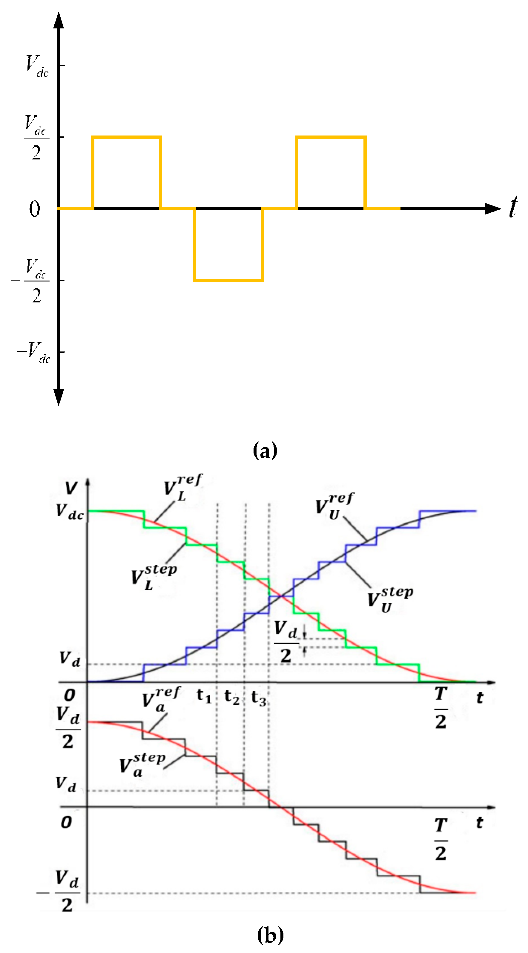
Similarly, when all the SMs in the lower arm are inserted and the SMs in the upper arm are bypassed, we will get an output voltage of ½ Vdc. When all the SMs in the upper arm are inserted, and the SMs in the lower arm are bypassed, we will obtain −½ Vdc. In case of an even number of levels, a zero output voltage cannot be obtained. The switching pattern of the SMs is shown in Table 1, and the waveform is displayed in Figure 3a.
We can conclude from the switching pattern that when all the SMs in the lower arm are inserted and the SMs in the upper arm are bypassed, we will observe a positive peak voltage. Similarly, when all the SMs in the upper arm are inserted and the SMs in the lower arm are bypassed, we will observe negative peaks in the output waveform. Using this concept, we can develop a switching pattern for any number of levels.

4. Proposed LabVIEW Multisim Co-Simulation Platform

LabVIEW is a graphical programming language that enables us to program the FPGA without using VHDL or Verilog. A nearest level control (NLC) algorithm was developed in LabVIEW to control the MMC operation and was compatible for deployment in real-time NI controllers (i.e., compact reconfigurable input/output (cRIO)). NLC is advantageous because the algorithm does not require complex changes when output waveform levels are increased for power quality analysis. Equations (13) and (14) are used to implement the NLC algorithm, where, Vd is the capacitor voltage, Vdc is the total DC link voltage, and NU and NL determine the total number of SMs to be inserted at any instant in the upper and lower arm, respectively.
N U = r o u n d 0.5 V d c 2 V d ( 1 + m cos ( ω t ) )
N L = r o u n d 0.5 V d c 2 V d ( 1 m cos ( ω t ) )

4.1. Open-Loop Results of MMC Co-Simulation

The open-loop NLC-based algorithm developed in LabVIEW for co-simulation is shown in Figure 4.
The inserted number of SMs can be calculated by Equations (13) and (14). The round function round0.5 (x) will round the real number x to the nearest whole number according to the decimal fraction of x. If the decimal fraction of x is greater than 0.5, x is rounded up to the next whole number, or else it is rounded down to the next whole number. To understand the switching states, two cases [t1 to t2, t2 to t3] are analyzed and shown in Figure 3b. In the first case [t1 to t2], assuming V L s t e p = M V d , then the reference values of the arm voltages and equivalent inner voltage of the phase at t = t1 can be shown as Equations (15) and (16), respectively.
{ V L r e f = ( M + 0.5 ) V d V U r e f = [ ( N M 1 ) + 0.5 ] V d
V E r e f = ( M 0.5 N + 0.5 ) V d
In the first scenario, the step waves of the arm voltages and equivalent inner voltage are expressed as
{ V L s t e p = M V d V U s t e p = ( N M ) V d
V E s t e p = ( M 0.5 N ) V d
In the second scenario, from t2 to t3, the reference values of the arm voltages and equivalent inner voltage are expressed as
{ V L r e f = [ ( M 1 ) + 0.5 ] V d V U r e f = [ ( N M ) + 0.5 ] V d
V E r e f = ( M 0.5 N 0.5 ) V d
The step waves of the arm voltages and equivalent inner voltage are shown as
{ V L s t e p = ( M 1 ) V d V U s t e p = ( N M + 1 ) V d
V E s t e p = ( M 0.5 N 1 ) V d
Comparing Equations (18) and (22), it can be observed that the step height in V E s t e p is V d . Since the positive and negative DC voltage limits are ±0.5Vdc, the maximum level in the equivalent inner voltage is equal to Vdc/Vd +1.
The solver methods recommended for co-simulation are R-K 23 and 45 ODE solvers since they can auto-adjust the rate of the loop according to the complexity of the circuit. The MMC model was designed in the NI Multisim software, and a half-bridge SM topology was considered for co-simulation. The sub-circuit for each arm was made as shown in Figure 5. An open simple RL load is considered for co-simulation.
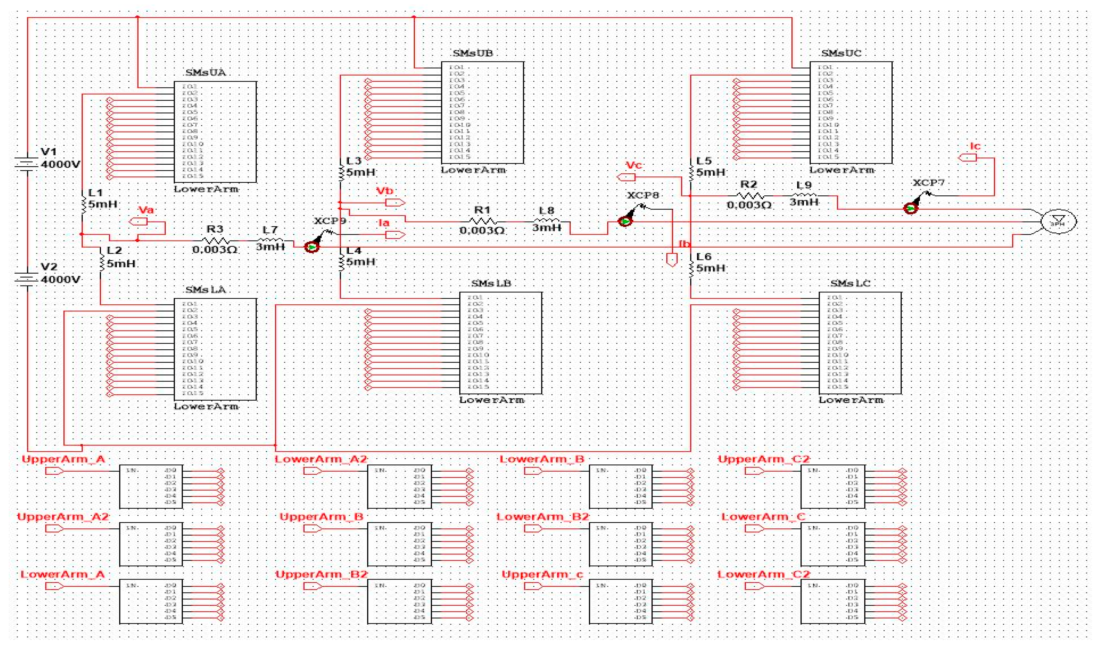
Each arm is an MMC that is connected by inductors to reduce the current change when all the SMs in the arm are bypassed and to limit the fault current. In Multisim, on-page connectors are used to distribute the signals coming from LabVIEW since only 24 inputs/outputs are allowed in LabVIEW Multisim co-simulation; however, they can be increased using decoders. The MMC circuit designed in Multisim is shown in Figure 6.
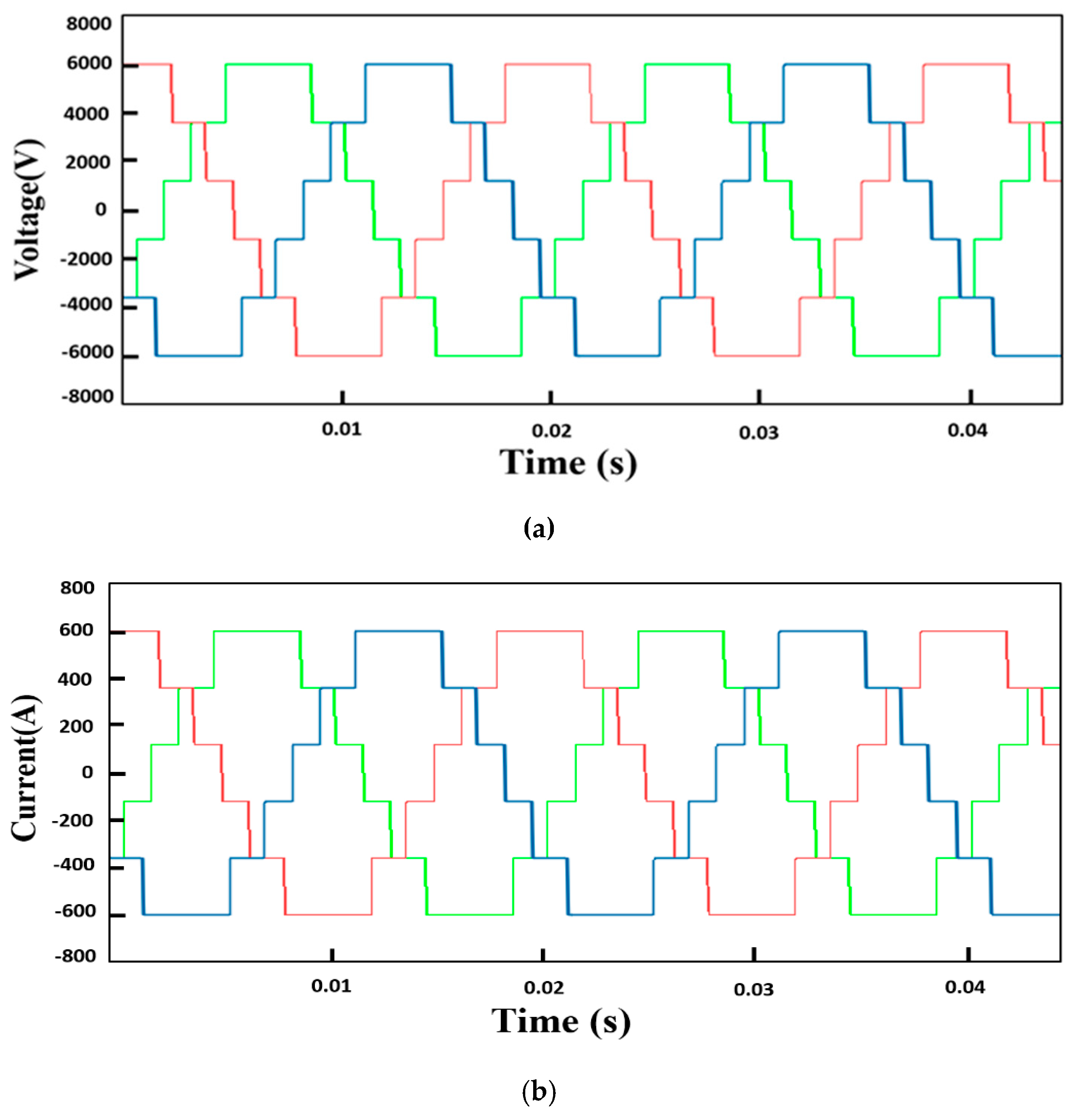
The open-loop MMC co-simulation was completed using an NLC control algorithm to obtain the results, and a simple RL load was considered. Capacitor voltage balancing was not considered. The output voltage waveform and current are shown in Figure 7.

4.2. Closed-Loop NLC Algorithm Design in LabVIEW

Modulation signals must be controlled and varied accordingly to control active and reactive power in a closed-loop MMC as depicted in Figure 8. The modulation signals are sinusoids and cannot be controlled instantaneously; therefore, two frames of reference are used: a stationary frame of reference or the alpha–beta frame, and a rotating frame of reference or the DQ frame. In LabVIEW, the DQ frame is used to achieve zero steady state errors with a pi controller.
Capacitor voltages in the MMC are not constant and need to be measured continuously whenever an SM is inserted or bypassed according to the direction of the arm current and value of the capacitor voltage. When the arm current is positive, capacitors are sorted from lowest to highest voltage, and capacitors with low voltages are inserted so they can be charged. In contrast, when the arm current is negative, capacitors are sorted from highest to lowest voltage, and the capacitors with high voltages are inserted so they can be discharged. In this experiment, the capacitor voltages were considered constant, and no voltage balancing algorithm was applied.
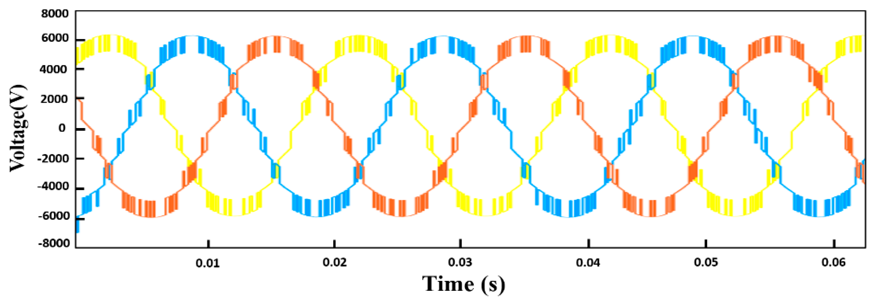
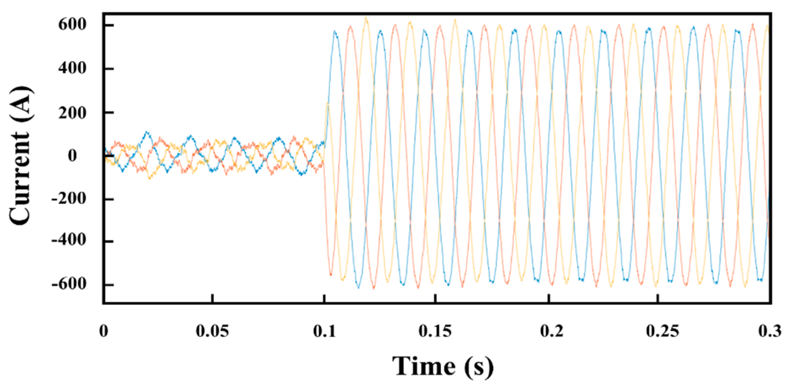
The output voltage and current were measured from the Multisim model node in LabVIEW as shown in Figure 9; Figure 10, respectively. In a closed-loop system, the output of the MMC is tied with the voltage source equivalent to grid. These measured parameters are fed back to the controller for active and reactive power control. The DQ reference frame was used to achieve zero steady state error.
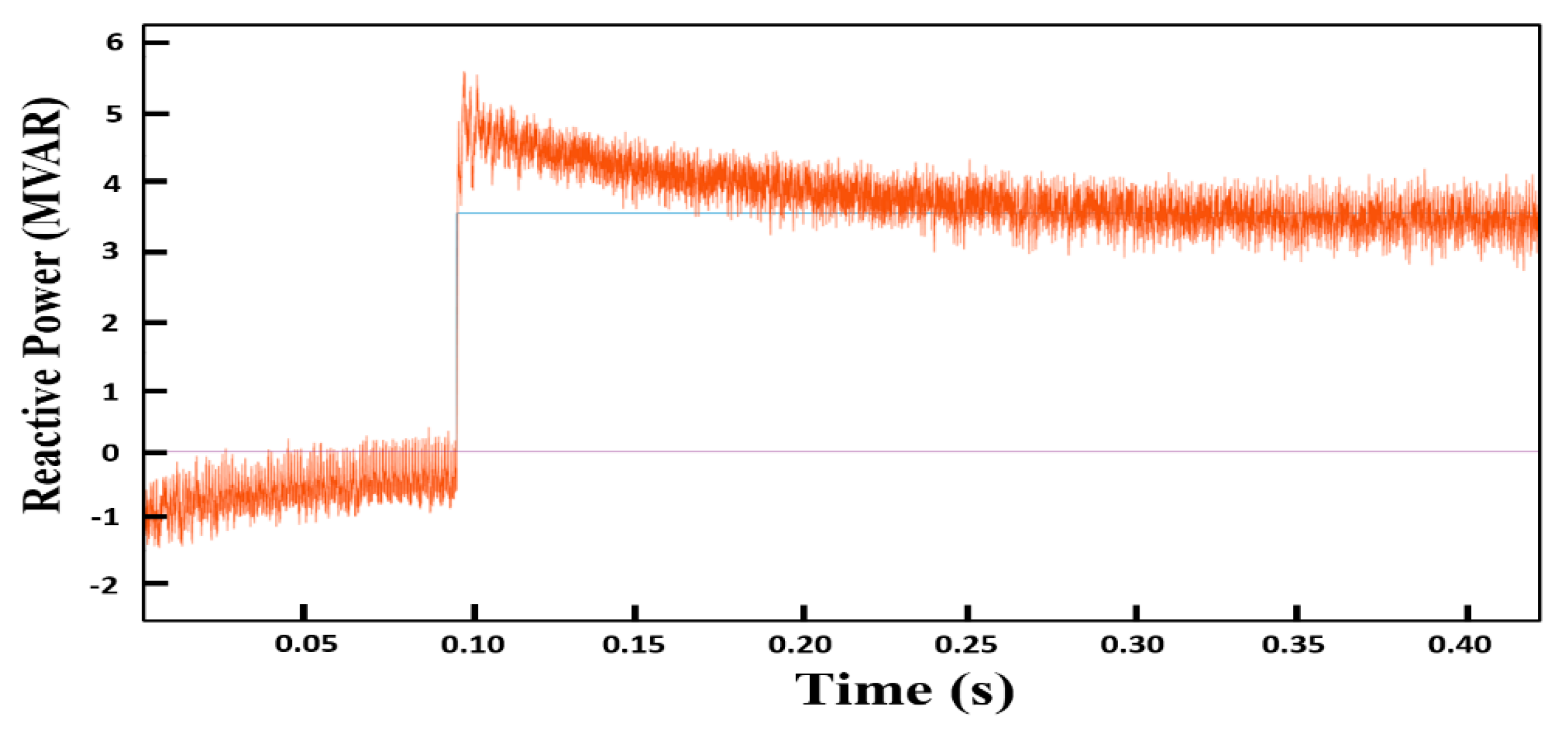
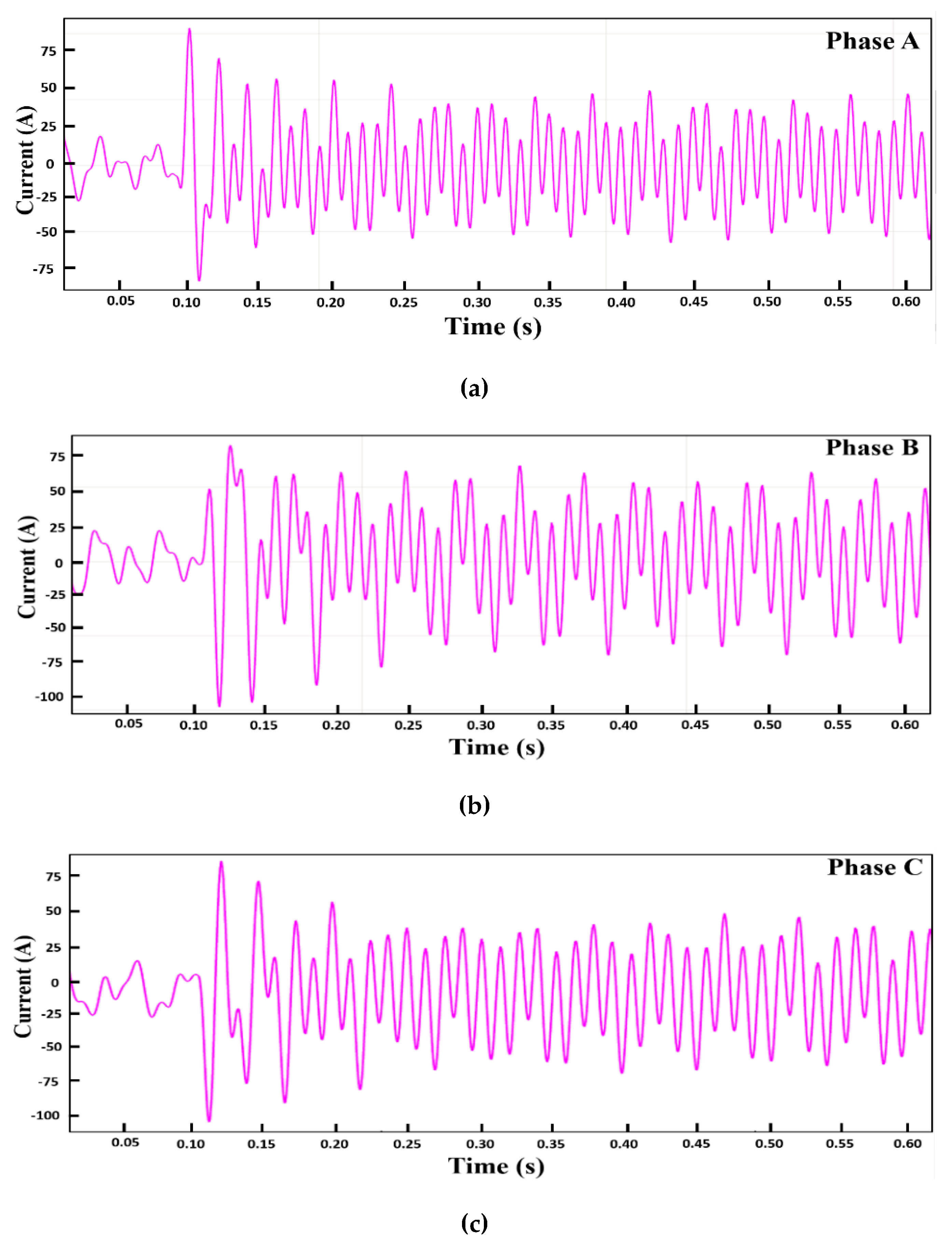
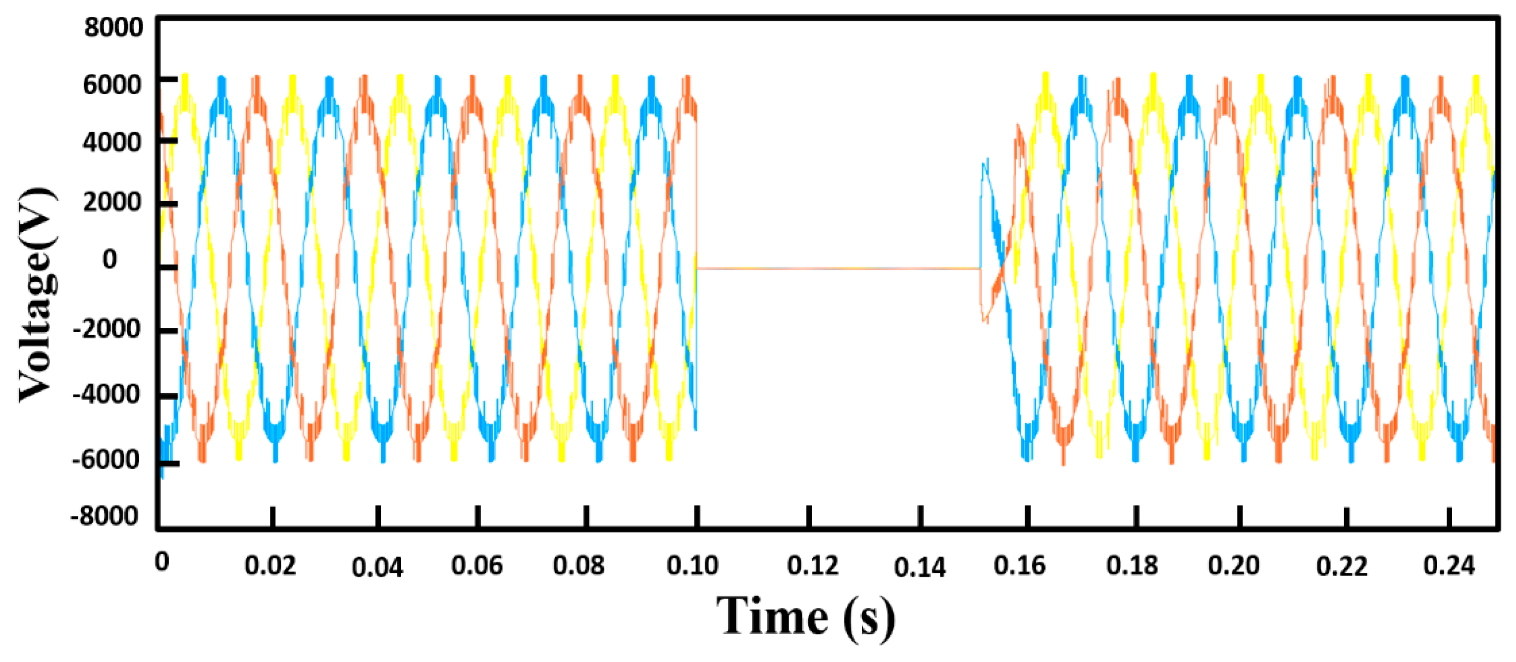
The active and reactive power controls were enabled at 0.1 s, and the observed response is shown in Figure 11 and Figure 12, respectively. The circulating current flowing in each phase of the MMC was found using Equation (12) and is shown in Figure 13, and it flows due to the potential difference between the upper and lower arm caused by the difference in SM capacitor voltage. Its magnitude must be reduced to zero in order to avoid losses in the MMC. Increasing the arm inductance decreases the circulating current but does not eliminate it. Its negative sequence component rotates at twice the line frequency. Different types of faults (i.e., line-to-line fault and three-phase fault) are also analyzed and shown in Figure 14 and Figure 15, respectively. The converter parameters are shown in Table 2.

5. Real-Time Control Algorithm Implementation and Testing in NI Compact RIO and PXIe

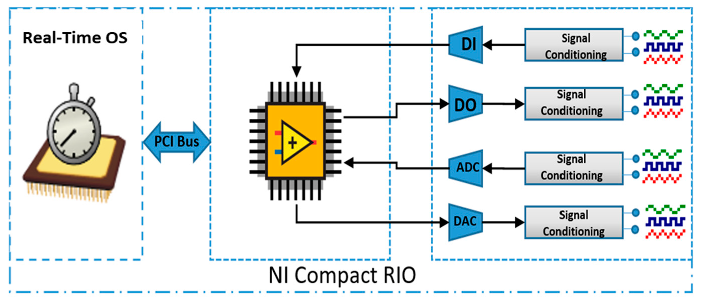
The compact RIO (cRIO) combines an RT operating system with an embedded floating-point processor. It has a remarkable FPGA performance and hot-swappable analogue and digital input/output modules with hardware flexibility. Each module in cRIO is directly connected to the FPGA, imparting minimum jitter and high-speed input/output signal processing. The FPGA is physically linked to the RT processor via a PCI bus as shown in Figure 16, which represents the internal architecture of the cRIO with an open retrieve to basic hardware resources. The FPGA and RT processor are programmed in LabVIEW, which is a graphical-language-based programming platform. LabVIEW has integrated data-fetching mechanisms to circulate data from the FPGA to the input/output modules and from the FPGA to the RT processor for real-time analysis, data logging, post-processing, and communication with the host computer.
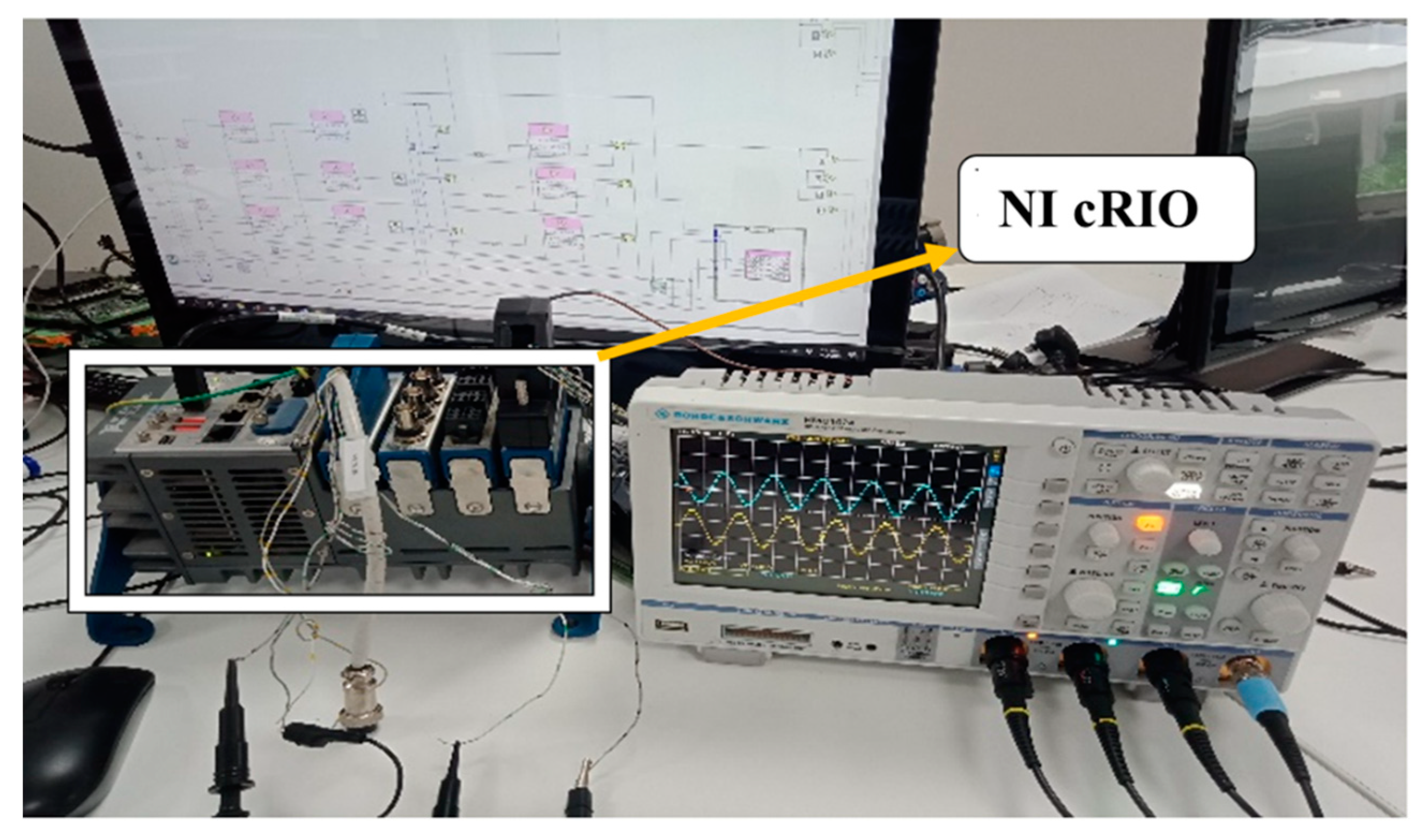
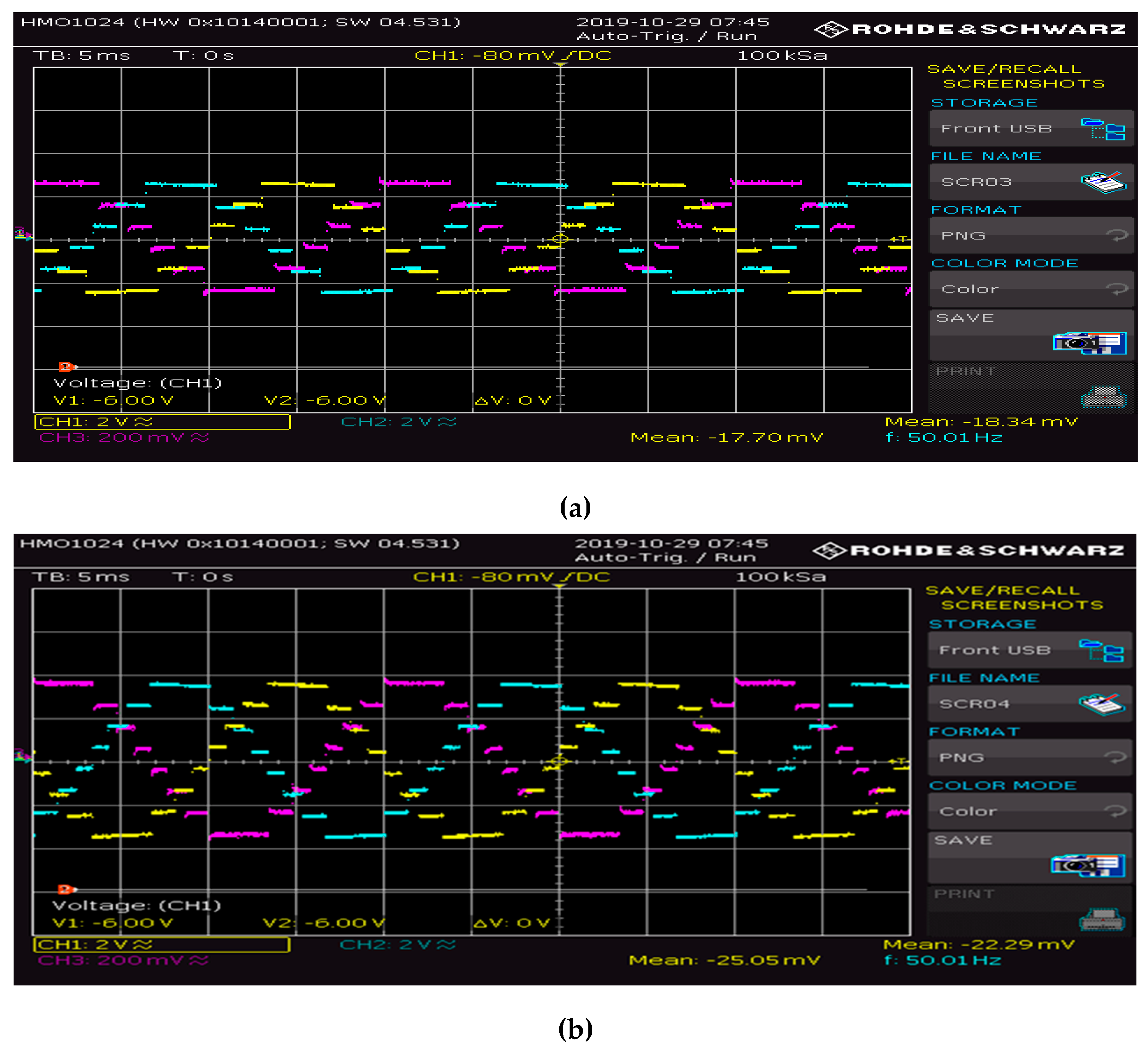
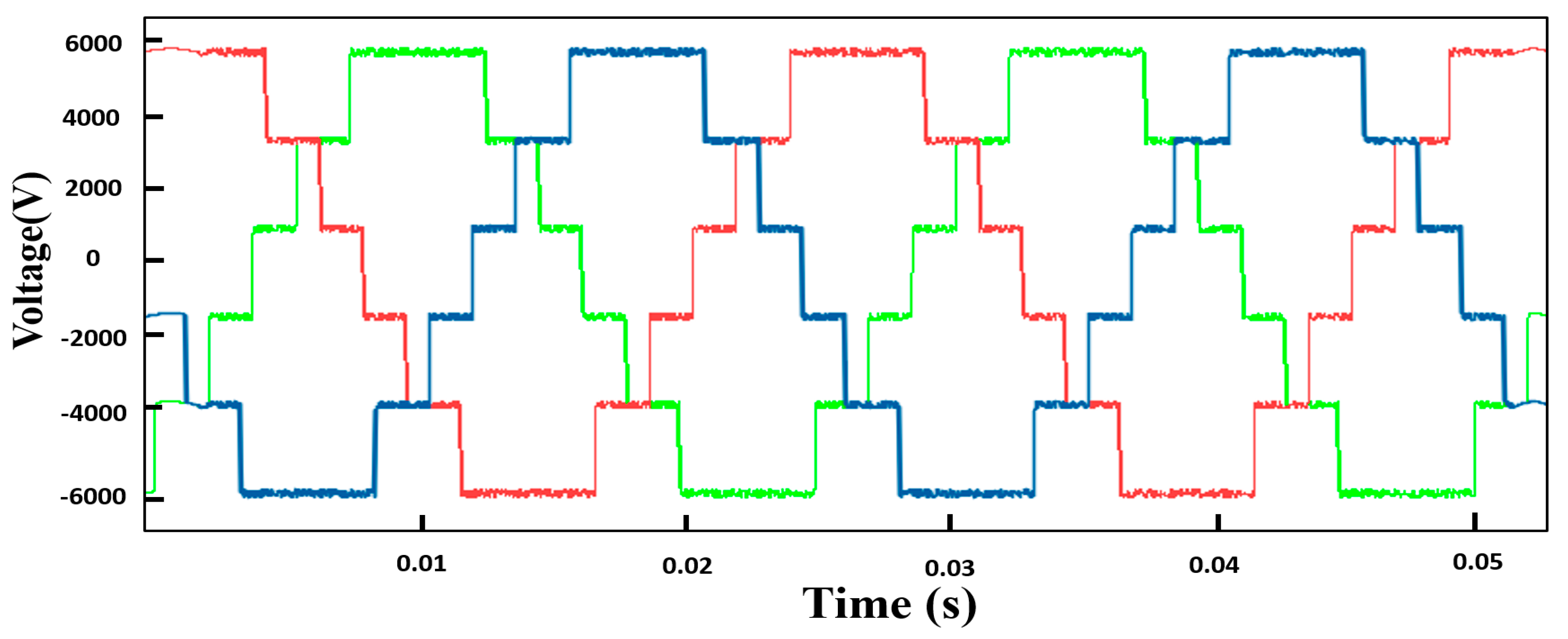
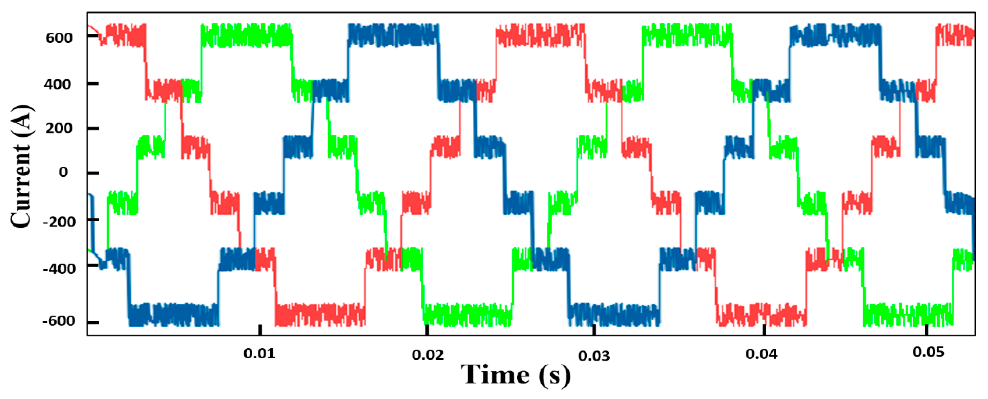
The control algorithm designed in LabVIEW was first compiled through the NI cloud servers and then downloaded in the NI cRIO FPGA to see the actual behavior of the controller. The algorithm was tested at different levels of the MMC, as shown in Figure 18. The system setup is shown in Figure 17, and the results obtained from the cRIO are shown in Figure 18; Figure 19. Once the controller showed the desired behavior, the signals generated from the cRIO were used to operate a real-time MMC circuit implemented in an NI FPGA-based PXIe system. The results obtained from the PXIe system are shown in Figure 20; Figure 21 and can be compared with the initially obtained results from the co-simulation.

6. State-of-the-Art Hardware-in-Loop Setup

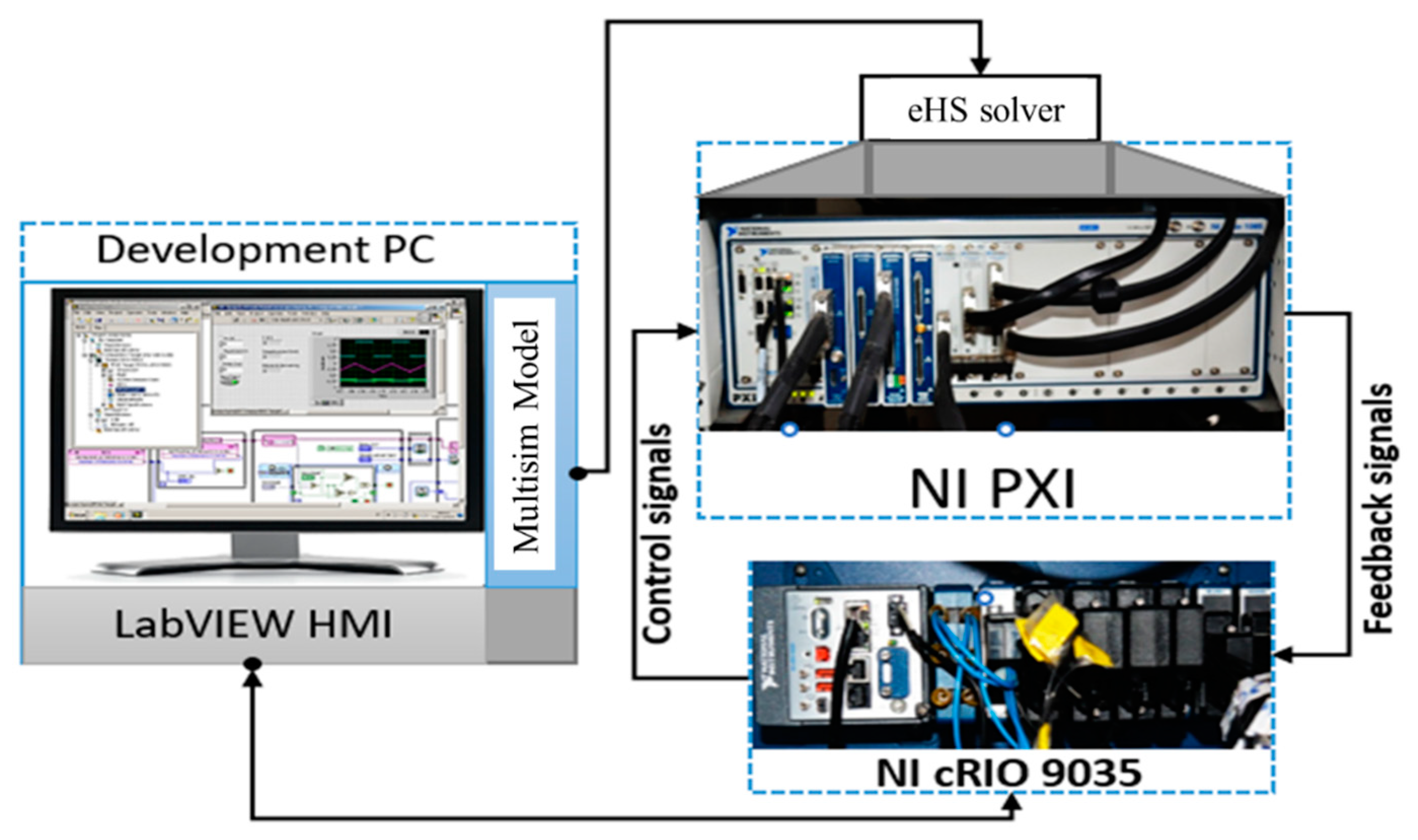
The hardware-in-loop (HIL) architecture helps the user to build a model in MATLAB/PLECS/PSIM/Multisim and burn it into PXI through an eHS solver provided by OPAL RT, which is an FPGA-based floating-point solver that helps the user to burn an electrical circuit on the FPGA automatically with a step size of 250 nanoseconds and without having to code in VHDL or calculating system equations. In our case, the minimum time step at which a model is loaded in PXI is 480 nanoseconds. The overall scheme of the RT system discussed above is shown in Figure 22. Initially, the co-simulation was performed using LabVIEW and Multisim on a desktop PC. After obtaining the results, the same developed algorithm on LabVIEW was burned on an FPGA-based real-time controller cRIO as shown in Figure 22. After getting satisfactory results from the controller, the real simulation was performed using an actual controller and PXIe system.
However, the total number of switches that can be used in one model is limited to 72 in PXIe. Additionally, there is a total of 64 analogue outputs that can be used as an input feedback to the controller cRIO from PXI.

7. Conclusions

Owing to an increased interest in HVDC MMCs, a platform where control algorithms are developed for simulations and deployed after the verification of the simulation results without changing the designed code is needed. In this study, a LabVIEW Multisim co-simulation platform was presented for designing a control algorithm that could be used to run the MMC circuit designed in Multisim and provide the simulation results. Now, once the simulation results are verified, the same algorithm can be loaded to NI controllers, such as the NI cRIO or myRIO, and the real-time controller can be used to control the real-time MMC burned in PXIe, which is a real-time digital simulator. Therefore, the use of this platform allows for obtaining simulation results and does not require changes to the code for real-time applications.

Author Contributions

Conceptualization, J.B., and F.A.; funding acquisition, J.-S.R.; investigation, S.A.; writing—review and editing, S.S.H.B. All authors have read and agreed to the published version of the manuscript.

Funding

This research received no external funding.

Acknowledgments

This research was supported in part by the Basic Science Research Program through the National Research Foundation of Korea funded by the Ministry of Education (2016R1D1A1B01008058); by the Human Resources Development (No. 20204030200090) of the Korea Institute of Energy Technology Evaluation and Planning (KETEP) funded by the Korean government’s Ministry of Trade, Industry, and Energy; and by the Korea Research Fellowship Program through the National Research Foundation (NRF) of Korea funded by the Ministry of Science and ICT (2019H1D3A1A01102988).

Conflicts of Interest

The authors declare no conflict of interest.

References

  1. Bidadfar, A.; Saborío-Romano, O.; Naidu Sakamuri, J.; Akhmatov, V.; Antonio Cutululis, N.; Ejnar Sørensen, P. Coordinated Control of HVDC and HVAC Power Transmission Systems Integrating a Large Offshore Wind Farm. Energies 2019, 12, 3435. [Google Scholar] [CrossRef] [Green Version]
  2. Kalair, A.; Abas, N.; Khan, N. Comparative study of HVAC and HVDC transmission systems. Renew. Sustain. Energy Rev. 2016, 59, 1653–1675. [Google Scholar] [CrossRef]
  3. Chachar, F.A.; Bukhari, S.S.H.; Mangi, F.H.; MacPherson, D.E.; Harrison, G.P.; Bukhsh, W.; Ro, J.-S.; Akhter, F.; Buhksh, W. Hierarchical Control Implementation for Meshed AC/Multi-Terminal DC Grids with Offshore Windfarms Integration. IEEE Access 2019, 7, 142233–142245. [Google Scholar] [CrossRef]
  4. Jamshidifar, A.; Jovcic, D. Small-Signal Dynamic DQ Model of Modular Multilevel Converter for System Studies. IEEE Trans. Power Deliv. 2015, 31, 191–199. [Google Scholar] [CrossRef] [Green Version]
  5. Li, C.; Hu, X.; Guo, J.; Liang, J. The DC grid reliability and cost evaluation with Zhoushan five-terminal HVDC case study. In Proceedings of the 2015 50th International Universities Power Engineering Conference (UPEC), Stroke-on-Trent, UK, 1–4 September 2015; pp. 1–6. [Google Scholar]
  6. Dekka, A.; Wu, B.; Zargari, N.R. A Novel Modulation Scheme and Voltage Balancing Algorithm for Modular Multilevel Converter. IEEE Trans. Ind. Appl. 2015, 52, 432–443. [Google Scholar] [CrossRef]
  7. Ishfaq, M.; Uddin, W.; Zeb, K.; Khan, I.; Islam, S.U.; Adil Khan, M.; Kim, H.-J. A New Adaptive Approach to Control Circulating and Output Current of Modular Multilevel Converter. Energies 2019, 12, 1118. [Google Scholar] [CrossRef] [Green Version]
  8. Hu, P.; Jiang, D.; Zhou, Y.; Liang, Y.; Guo, J.; Lin, Z. Energy-Balancing Control Strategy for Modular Multilevel Converters under Submodule Fault Conditions. IEEE Trans. Power Electron. 2013, 29, 5021–5030. [Google Scholar] [CrossRef]
  9. Mehrasa, M.; Pouresmaeil, E.; Taheri, S.; Vechiu, I.; Catalão, J.P. Novel Control Strategy for Modular Multilevel Converters Based on Differential Flatness Theory. IEEE J. Emerg. Sel. Top. Power Electron. 2017, 6, 888–897. [Google Scholar] [CrossRef] [Green Version]
  10. Cui, S.; Kim, S.; Jung, J.-J.; Sul, S.-K. A comprehensive cell capacitor energy control strategy of a modular multilevel converter (MMC) without a stiff DC bus voltage source. In Proceedings of the 2014 IEEE Applied Power Electronics Conference and Exposition—APEC 2014, Fort Worth, TX, USA, 16–20 March 2014; pp. 602–609. [Google Scholar]
  11. Li, K.; Yuan, L.; Zhao, Z.; Lu, S.; Zhang, Y. Fault-Tolerant Control of MMC With Hot Reserved Submodules Based on Carrier Phase Shift Modulation. IEEE Trans. Power Electron. 2016, 32, 6778–6791. [Google Scholar] [CrossRef]
  12. Lee, Y.; Cui, S.; Kim, S.; Sul, S.-K. Control of hybrid HVDC transmission system with LCC and FB-MMC. In Proceedings of the 2014 IEEE Energy Conversion Congress and Exposition (ECCE), Pittsburgh, PA, USA, 13–18 September 2014; pp. 475–482. [Google Scholar]
  13. Zhou, Y.; Jiang, D.; Hu, P.; Guo, J.; Liang, Y.; Lin, Z. A Prototype of Modular Multilevel Converters. IEEE Trans. Power Electron. 2013, 29, 3267–3278. [Google Scholar] [CrossRef]
  14. Moranchel, M.; Sánchez, F.M.; Bueno, E.J.; Rodriguez, F.J.; Sanz, I. Six-Level modular multilevel converter prototype with centralized hardware platform controller. In Proceedings of the IECON 2015—41st Annual Conference of the IEEE Industrial Electronics Society, Yokohama, Japan, 9–12 November 2015; pp. 3863–3868. [Google Scholar]
  15. Schnarrenberger, M.; Kammerer, F.; Brackle, D.; Braun, M. Cell design of a square-wave powered 1AC-3AC modular multilevel converter low voltage prototype. In Proceedings of the 2016 18th European Conference on Power Electronics and Applications (EPE’16 ECCE Europe), Karlsruhe, Germany, 5–9 September 2016; pp. 1–11. [Google Scholar]
  16. Wang, Z.; Hua, L.; Ma, Y. A Control Strategy of Modular Multilevel Converter with Integrated Battery Energy Storage System Based on Battery Side Capacitor Voltage Control. Energies 2019, 12, 2151. [Google Scholar] [CrossRef] [Green Version]
  17. Hakimi, S.M.; Hajizadeh, A. Integration of Photovoltaic Power Units to Power Distribution System through Modular Multilevel Converter. Energies 2018, 11, 2753. [Google Scholar] [CrossRef] [Green Version]
  18. Yin, J.; Wu, W.; Tongzhen, W.; Xuezhi, W.; Qunhai, H. A Novel Fault-Tolerant Control of Modular Multilevel Converter under Sub-Module Faults based on Phase Disposition PWM. Energies 2018, 12, 20. [Google Scholar] [CrossRef] [Green Version]
  19. Kim, K.-M.; Kim, J.-H.; Kim, D.-H.; Han, B.-M.; Lee, J.Y. Improved Pre-Charging Method for MMC-Based HVDC Systems Operated in Nearest Level Control. J. Power Electron. 2017, 17, 127–135. [Google Scholar] [CrossRef] [Green Version]
  20. Talon Louokdom, E.; Gavin, S.; Siemaszko, D.; Biya-Motto, F.; Essimbi Zobo, B.; Marchesoni, M.; Carpita, M. Small-Scale Modular Multilevel Converter for Multi-Terminal DC Networks Applications: System Control Validation. Energies 2018, 11, 1690. [Google Scholar] [CrossRef] [Green Version]
  21. Andrus, M.; Ravindra, H.; Hauer, J.; Steurer, M.; Bosworth, M.; Soman, R. PHIL implementation of a MVDC fault management test bed for ship power systems based on megawatt-scale modular multilevel converters. In Proceedings of the 2015 IEEE Electric Ship Technologies Symposium (ESTS), Old Town Alexandria, VA, USA, 21–24 June 2015; pp. 337–342. [Google Scholar]
  22. Liang, T.; Dinavahi, V. Real-Time Device-Level Simulation of MMC-Based MVDC Traction Power System on MPSoC. IEEE Trans. Transp. Electrific. 2018, 4, 626–641. [Google Scholar] [CrossRef]
  23. Blaszczyk, P.; Steurer, M.; Soto, D.; Bogdan, F.; Hauer, J.; Sloderbeck, M.; Schoder, K. Modular multilevel converter based test bed for mvdc applications—A case study with a 12 kV, 5 MW setup. In Proceedings of the 2016 IEEE International Power Electronics and Motion Control Conference (PEMC), Varna, Bulgaria, 25–30 September 2016; pp. 139–145. [Google Scholar]
  24. Zhang, S.; Wang, S.; Praisuwanna, N.; Kong, L.; Li, Y.; Martin, R.B.; Wang, F.; Tolbert, L.M. Development of a Flexible Modular Multilevel Converter Test-Bed. In Proceedings of the 2018 IEEE Energy Conversion Congress and Exposition (ECCE), Portland, OR, USA, 24–27 September 2018; pp. 5250–5257. [Google Scholar]
  25. Guillaud, X.; Faruque, M.O.; Teninge, A.; Hariri, A.H.; Vanfretti, L.; Paolone, M.; Dinavahi, V.; Mitra, P.; Lauss, G.; Dufour, C.; et al. Applications of Real-Time Simulation Technologies in Power and Energy Systems. IEEE Power Energy Technol. Syst. J. 2015, 2, 103–115. [Google Scholar] [CrossRef] [Green Version]
  26. Li, Y.; Shi, X.; Liu, B.; Lei, W.; Wang, F.; Tolbert, L.M. Development, Demonstration, and Control of a Testbed for Multiterminal HVDC System. IEEE Trans. Power Electron. 2017, 32, 6069–6078. [Google Scholar] [CrossRef]
  27. Steurer, M.M.; Schoder, K.; Faruque, O.; Soto, D.; Bosworth, M.; Sloderbeck, M.; Bogdan, F.; Hauer, J.; Winkelnkemper, M.; Schwager, L.; et al. Multifunctional Megawatt-Scale Medium Voltage DC Test Bed Based on Modular Multilevel Converter Technology. IEEE Trans. Transp. Electrific. 2016, 2, 597–606. [Google Scholar] [CrossRef]
  28. Wang, L.; Bosworth, M.; Hauer, J.; Soto, D.; Schoder, K.; Steurer, M. Common-Mode Characterization of a Modular Multilevel Converter in a Megawatt-scale Medium-Voltage DC Test Bed. In Proceedings of the 2019 IEEE Electric Ship Technologies Symposium (ESTS), Washington, DC, USA, 14–16 August 2019; pp. 388–395. [Google Scholar]
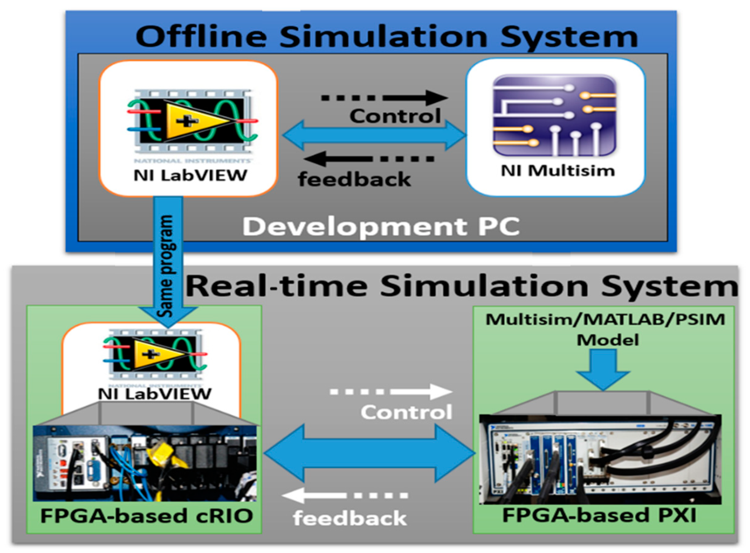
Figure 1. LabVIEW Multisim co-simulation block diagram.
Applsci 10 06004 g001
Figure 2. (a) Single-phase modular multilevel converter (MMC) circuit diagram; (b) equivalent circuit of the MMC.
Applsci 10 06004 g002
Figure 3. (a) Switching pattern of the output waveform; (b) switching states of the reference and output waveform.
Applsci 10 06004 g003
Figure 4. Open-loop control algorithm development in LabVIEW for the MMC.
Applsci 10 06004 g004
Figure 5. Sub-circuit of each arm in National Instruments (NI) Multisim.
Applsci 10 06004 g005
Figure 6. MMC circuit designed in NI Multisim.
Applsci 10 06004 g006
Figure 7. Three-phase 6-level output (a) voltage and (b) current waveforms of the MMC.
Applsci 10 06004 g007
Figure 8. Closed-loop control algorithm development in LabVIEW for the MMC.
Applsci 10 06004 g008
Figure 9. Output voltage of the closed-loop MMC LabVIEW Multisim co-simulation.
Applsci 10 06004 g009
Figure 10. Output current flowing into grid.
Applsci 10 06004 g010
Figure 11. Active power control of the MMC in the LabVIEW Multisim co-simulation.
Applsci 10 06004 g011
Figure 12. Reactive power control of the MMC in the LabVIEW Multisim co-simulation.
Applsci 10 06004 g012
Figure 13. Circulating current flowing in each phase of the MMC: (a) phase A, (b) phase B, and (c) phase C.
Applsci 10 06004 g013
Figure 14. Line-to-line fault.
Applsci 10 06004 g014
Figure 15. Three-phase symmetrical fault.
Applsci 10 06004 g015
Figure 16. NI compact reconfigurable input/output (cRIO) architecture.
Applsci 10 06004 g016
Figure 17. NI cRIO-based setup for real-time control algorithm testing.
Applsci 10 06004 g017
Figure 18. (a) 6-level MMC control staircase waveform; (b) eight-level MMC control staircase waveform.
Applsci 10 06004 g018
Figure 19. Switching signal for SM operation in the MMC.
Applsci 10 06004 g019
Figure 20. Three-phase 6-level output voltage from PXIe.
Applsci 10 06004 g020
Figure 21. Three-phase 6-level output current from PXIe.
Applsci 10 06004 g021
Figure 22. Experimental setup of hardware-in-loop (HIL) architecture.
Applsci 10 06004 g022
Table 1. Switching pattern of the submodules (SMs) for a 3-level MMC.
1-PhaseSM NumberOutput Voltage Levels
0½ Vdc0−½ Vdc0½ Vdc0
Upper ArmSM1
SM2
Lower ArmSM1
SM2
Table 2. System parameters and values.
Item No.System ParametersValues
1Rated power 10 MVA
2Vac grid voltage4.16 kV
3Vdc8 kV
4Switching frequency300 Hz
5Rated frequency50 Hz
6SM_cap (submodule capacitance)5000 μF
7L_arm (arm inductance)5 mH
8L_val (line inductance)3 mH
9R_line (line resistance)0.003 Ω