Article

Air Pressure, Gas Exposure and Electron Beam Irradiation of 2D Transition Metal Dichalcogenides

by
Antonio Di Bartolomeo
1,2,*,
Aniello Pelella
1,
Alessandro Grillo
1,
Francesca Urban
1 and
Filippo Giubileo
2,*
1
Department of Physics ‘E.R.Caianello’, University of Salerno, Via Giovanni Paolo II 132, 84084 Fisciano (SA), Italy
2
CNR-SPIN Institute, Via Giovanni Paolo II 132, 84084 Fisciano (SA), Italy
*
Authors to whom correspondence should be addressed.
Appl. Sci. 2020, 10(17), 5840; https://doi.org/10.3390/app10175840
Submission received: 19 June 2020 / Revised: 26 July 2020 / Accepted: 20 August 2020 / Published: 23 August 2020
(This article belongs to the Special Issue 10th Anniversary of Applied Sciences: Invited Papers in Materials)

Abstract

:
In this study, we investigate the electrical transport properties of back-gated field-effect transistors in which the channel is realized with two-dimensional transition metal dichalcogenide nanosheets, namely palladium diselenide (PdSe2) and molybdenum disulfide (MoS2). The effects of the environment (pressure, gas type, electron beam irradiation) on the electrical properties are the subject of an intense experimental study that evidences how PdSe2-based devices can be reversibly tuned from a predominantly n-type conduction (under high vacuum) to a p-type conduction (at atmospheric pressure) by simply modifying the pressure. Similarly, we report that, in MoS2-based devices, the transport properties are affected by pressure and gas type. In particular, the observed hysteresis in the transfer characteristics is explained in terms of gas absorption on the MoS2 surface due to the presence of a large number of defects. Moreover, we demonstrate the monotonic (increasing) dependence of the width of the hysteresis on decreasing the gas adsorption energy. We also report the effects of electron beam irradiation on the transport properties of two-dimensional field-effect transistors, showing that low fluences of the order of few e-/nm2 are sufficient to cause appreciable modifications to the transport characteristics. Finally, we profit from our experimental setup, realized inside a scanning electron microscope and equipped with piezo-driven nanoprobes, to perform a field emission characterization of PdSe2 and MoS2 nanosheets at cathode–anode separation distances as small as 200 nm.

1. Introduction

The exceptional properties of two-dimensional (2D) materials have focused an enormous amount of research activity on developing next-generation devices in the field of electronics and optoelectronics [1]. Graphene had the merit of being the prototype of these 2D materials and it is extremely interesting as a transparent electrode, but, being a gapless semiconductor, has several drawbacks in its digital logic and optoelectronic applications [2]. In this context, transition metal dichalcogenides (TMDs), such as MoS2, WS2, WSe2, PdSe2, and many others, were recognized as valid candidates to be exploited in those fields, due to their physical and chemical properties, including a finite band gap tuned by the number of layers, the absence of dangling bonds, chemical stability, etc. [3,4,5,6].
In this study, we report a detailed investigation of the effects caused by pressure, gas type and electron beam irradiation on the electrical transport properties of back-gated field-effect transistors with PdSe2 or MoS2 nanosheets as conducting channels. We demonstrate that the conduction of the devices can be tuned from the n-type (dominant in a high vacuum) to the p-type by modifying the gas pressure. In addition, the transfer characteristics are significantly modified by the gas absorption, showing a widening of the observed hysteresis.
Interestingly, we also show that the transport properties are clearly affected by electron bombardments at fluences as low as those typically involved in electron beam-based imaging and processing techniques. Finally, we report a characterization of the field emission properties of the nanosheets under investigation. Their n-type conduction as well as their high aspect ratio at the borders allow us to extract a current at the relatively low electric fields applied. These field emission properties open up new opportunities for the exploitation of 2D materials in vacuum electronics.

2. Materials and Methods

Back-gated field-effect transistors were fabricated on Si (highly p-doped)/SiO2 (300-nm-thick) substrates with mechanically exfoliated PdSe2 [7] and chemical vapor deposition (CVD) MoS2 nanosheets [8,9]. The standard scotch tape method was applied to exfoliate single PdSe2 crystals that had been synthesized via a thermal process of compressed tablets of selenium and palladium powders, mixed in an atomic ratio of 2:1 and held in a quartz tube at 850 °C and 7.5 µTorr for 72 h. The thermal cycle was repeated twice, the second time after mixing the PdSe2 tablets with Se powder in a mass ratio of 1:4.
MoS2 nanoflakes were obtained by CVD in a three-zone tube furnace, purged with Ar gas for 15 min to minimize the O2 content. S powder was located upstream in a zone heated to 150 °C, while the Si/SiO2 substrate and the MoO3 precursor were placed in a downstream zone of the furnace, heated to 750 °C. The deposition process lasted 15 min, after which the sample was cooled down rapidly.
PdSe2 has a pentagonal and puckered structure (Figure 1a), while MoS2 has a hexagonal and planar structure (Figure 1b) [10,11].
Nanosheets for this study were initially identified by optical microscopy and then confirmed by Raman spectroscopy. Furthermore, scanning electron microscopy (SEM) and atomic force microscopy (AFM) were employed to characterize the nanosheets’ lateral size and thickness. While exfoliated PdSe2 nanoflakes were multilayers with thicknesses around 15 nm, MoS2 nanosheets were mostly monolayer or bilayers with thicknesses below 1.3 nm. Details regarding the materials’ fabrication and characterization have been reported elsewhere [7,8,9,12,13]. Electron beam lithography and a standard lift-off process were used to realize Ti(5 nm)/Au(40 nm) metallic electrodes contacting the nanosheets. In Figure 1c,d, we report a top-view SEM image of a back-gated field-effect transistor fabricated using a PdSe2 (MoS2) nanosheet as the channel and Ti/Au leads as the metal contacts.
The electrical measurements were performed inside a scanning electron microscope chamber, equipped with piezo-driven nanoprobes connected to a Keithley 4200 SCS (a semiconductor parameter analyzer by Tektronix Inc, Beaverton, Oregon) working as multi-source-measurement units. Metal leads were used as the source and drain electrodes in a three-terminal configuration, the back gate being realized by the Si substrate. The fabrication of more than two top electrodes allowed us to characterize more than one transistor on the same nanosheet to verify the sample homogeneity.

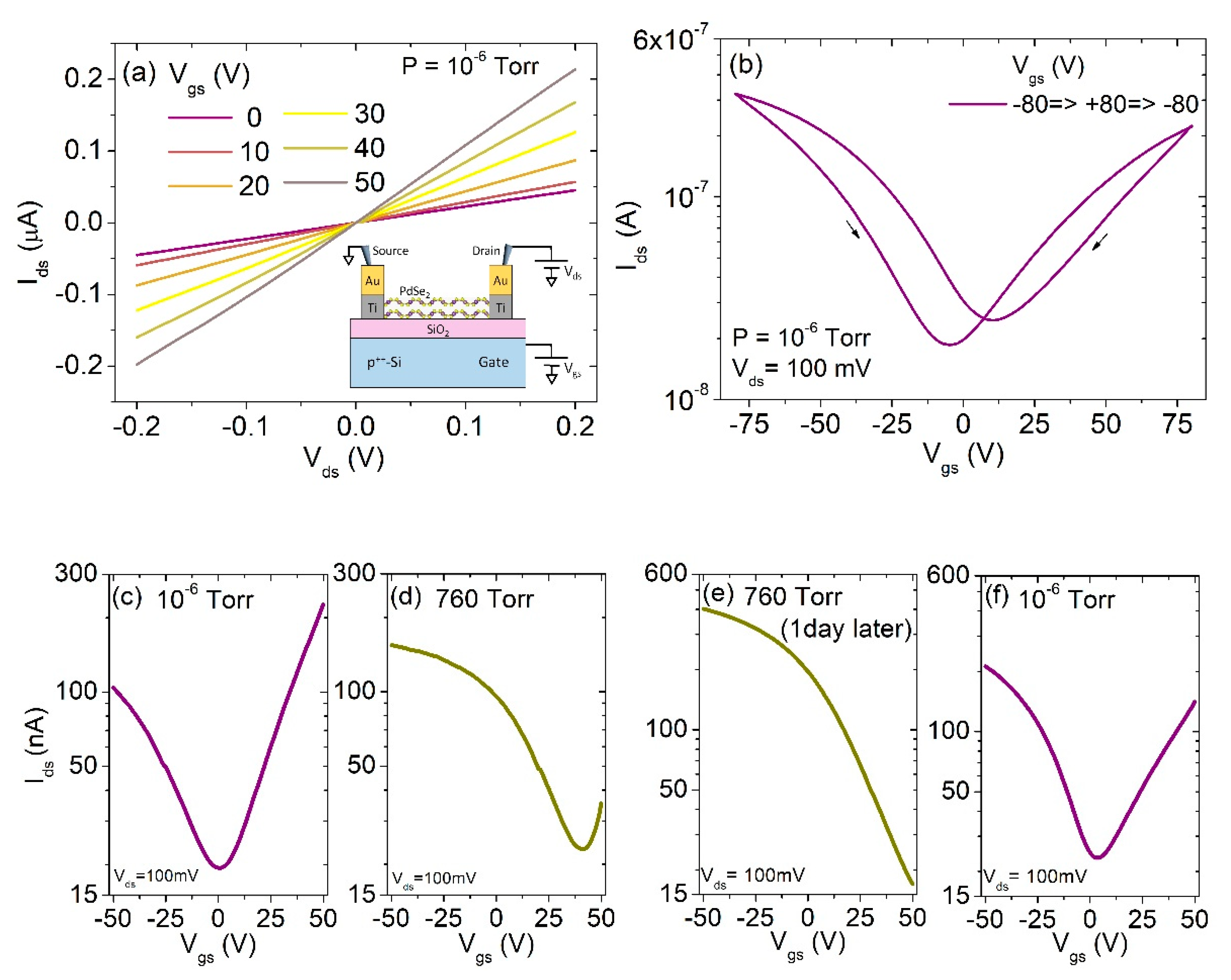
3. Results and Discussion

The electrical characterization of the PdSe2 back-gated field-effect transistor is reported in Figure 2. The drain-source current-voltage, Ids–Vds, output characteristics (Figure 2a), measured in a high vacuum and at room temperature, are linear and demonstrate the formation of a good ohmic contact between PdSe2 and Ti. The Ids–Vgs transfer curve, reported in Figure 2b, was measured by fixing a bias Vds = 100 mV between the source and the drain, and sweeping the gate bias Vgs forward from −80 V to +80 V and then backward from +80 V to −80 V. The transfer curve has a hysteretic behavior, often observed in 2D material-based field effect transistors (FET), and it can be explained in terms of adsorbates on the channel surface, trap states in the dielectric or at the dielectric/channel interface or due to intrinsic defects [7,14,15,16]. In particular, trap states can be filled (or emptied) during the gate bias sweep and can participate in the gating effect, originating the hysteresis [17,18].
The measured curve shows a clear ambipolar behavior and a current modulation of about one order of magnitude. The observed ambipolar behavior gives an indication that we are dealing with a semiconducting material characterized by a small band gap. We note that the band gap amplitude is expected to depend on the number of layers. According to the nanosheet characterization, the PdSe2 layer under investigation is about 15-nm thick, i.e., about 25 layers [10], which should correspond to a bandgap less than 100 meV [19]. The transfer curve reported in Figure 2b shows a conductance minimum at about Vgs = 0 V that is indicative of the midgap alignment of the Fermi levels of the contacts. These curves also allowed us to obtain an estimation of the field-effect mobility, using the following equation:
µ = L W ( 1 C SiO 2 · V ds ) · dI ds dV gs
where L and W are the channel length and width, respectively, and CSiO2 is the capacitance per unit area of SiO2. We can calculate C SiO 2 = ( ϵ 0 · ϵ SiO 2 ) t SiO 2 =   0.11 · 10−3 F/m2, considering that ϵ 0 is the vacuum permittivity, ϵ SiO 2   = 3.9 is the relative permittivity of SiO2 and t SiO 2   = 300 nm is the thickness of SiO2. Then, evaluating the slope dI ds dV gs of the I ds   V gs curve in the linear region, we obtain the field-effect mobility, μ   3.0 cm2V−1s−1, within the range of values typically reported (0.01–100 cm2V−1s−1) for TMD-based FETs on SiO2 [20,21,22,23,24,25]. In Figure 2c–f, we report the evolution of the transfer characteristics measured in the presence of different pressure conditions, i.e., at atmospheric pressure and in a high vacuum (10−6 Torr), in order to verify the effects of the pressure on the transistor properties. We first show the curve measured in a high vacuum (Figure 2c) and then the curve measured at 760 Torr (Figure 2d). The pressure was raised gradually by controlling the air flow via a high precision vacuum valve. We observe that the Ids–Vgs transfer curve shifts towards a positive bias that means a change from n-type to p-type conduction in the investigated gate bias range. By keeping the device exposed to air (atmospheric pressure) for about 8 h, the p-type behavior is further enhanced (Figure 2e), with no indication of ambipolarity. Successively, by reducing the pressure back to 10−6 Torr, we demonstrate (in Figure 2f) that the process can be reversed by restoring the ambipolar conduction centered almost at Vgs = 0 V. The reversibility of this phenomenon provides an opportunity to use the pressure as a controller to tune the conduction type from n to p or vice versa in PdSe2 devices. However, it has been reported that long air exposure (>15 days) can result in the definitive suppression of n-type conduction [26]. The observed reversible conduction type can be due to the activated chemisorption of molecular O2, probably in the Se vacancies, and desorption by vacuum annealing [7,26].
A similar characterization of the effect of pressure on the transport properties of 2D field-effect transistors was performed on monolayer MoS2-based devices. In Figure 3a, we report the Ids–Vds output characteristics, measured for different values of the gate voltage. The experimental data evidence a clear modulation of the current up to five orders of magnitude and an asymmetric behavior. Usually, the Fermi level at the metal–MoS2 interface is pinned above the midgap of MoS2 by either a metal work function modification due to interface dipole formation or by the production of gap states owing to the intralayer S–Mo bonding being weakened by metal [27]. As a consequence of the Fermi level pinning, Schottky barriers are formed at the contacts, causing the small rectification observed in the output curves as well as a dominant n-type behavior [9,28,29].
In Figure 3b we show a I ds   V gs transfer curve, measured in a high vacuum (10−6 Torr) and at room temperature, by applying a bias V ds   = 100 mV. We note that the device has the expected n-type conduction and clear hysteresis. In addition, we estimate a field-effect mobility of about 1 cm2V−1s−1 and an on-off ratio of about six orders of magnitude. The I ds   V gs transfer curves at atmospheric pressure (Figure 3c,d) were then measured by filling the SEM chamber with selected gases. We observe that the exposure to gas provokes significant modifications of the curves, in particular causing a reduction in the conductance and/or a widening of the hysteresis. More precisely, we stress that when monolayer MoS2 FET is exposed to argon or hydrogen atmospheric pressure, the main effect is the enlargement of the hysteresis, keeping the same conductance values at the maximum (positive and negative) gate bias (Figure 3c). On the other hand, when oxygen, nitrogen, and methane are employed, a reduction in the conductance is also observed (Figure 3d). In all cases, the device remains in the n-type conduction due to the intrinsic doping of MoS2 by S vacancies and to the pinning effect [27,30]. Moreover, S vacancies and other defects like unreacted MoO3 play a role as centers for gas adsorption [8], favoring charge trapping and an increase in the hysteresis.
From the curves of Figure 3c,d, we can obtain the relation between the hysteresis width, Hw (here defined as the Vgs difference at 10 pA current) and the gas adsorption energy Eads [31,32,33]. The results are summarized in Table 1. Eads are ordered for increasing absolute value to evidence the monotonic dependence of Hw on Eads.
To complete the characterization of the transport properties in PdSe2- (Figure 4a) and MoS2-based (Figure 4b) field-effect transistors, we also investigated the effect of electron beam irradiation. Indeed, 2D materials are necessarily exposed to electron irradiation during fabrication or imaging processes, as in electron beam lithography or simply in SEM imaging. To measure such an effect, we performed an experiment in the SEM chamber using a 10 keV-electron beam to irradiate the nanosheets at various fluences. We clarify here that electrical measurements were performed soon after each irradiation (when the beam is switched off). The first I ds V gs transfer curve was measured in its pristine state, before the irradiation, and was compared to the curves measured for successively increasing levels of fluences up to 4160 e/nm2 for PdSe2 (Figure 4c) and up to 100 e/nm2 for MoS2 (Figure 4d).
From the data in Figure 4c, we note that electron irradiation causes a suppression of the n-type conduction towards a p-type conduction. On the other hand, from Figure 4d, we see that n-type conduction is enhanced in the MoS2 device. Comparing the two behaviors, it seems that electron irradiation acts with opposite modifications on PdSe2 and in MoS2 devices. Actually, it has been reported that effects on PdSe2 may be irreversible [34], differing from MoS2, in which vacuum annealing can restore its initial state [35]. To explain the experimental observations, we need to take into account that electron irradiation can easily produce Se and S vacancies, due to the small energy (less than 10 eV) necessary for the displacement of a chalcogen atom [36]. Vacancy formation is responsible for p-type conductivity, in particular when dealing with thick nanosheets (as in the case of 15-nm-thick PdSe2), in which a larger beam energy can be adsorbed [34].
A further effect of electron irradiation is the formation of electron–hole pairs in both the SiO2 oxide and the Si substrate. Therefore, holes may accumulate in the oxide (while electrons are easily transported away by the bias) causing a gating effect that increases the n-type doping. This process is dominant for MoS2, where there is a limited release of energy and negligible S displacement because of the atomic thickness.
Our results are of interest to evaluate the radiation hardness of 2D materials to develop devices working in high radiation environments (such as space or nuclear plants).
Finally, we also performed a complete field emission characterization of PdSe2 and MoS2 nanosheets, to profit from the sharp edges of 2D materials as well as from a work function that, in these materials, decreases with the decreasing number of layers [37] (4.3 eV in monolayer PdSe2 [19] and about 4.4 in monolayer MoS2 [38]). The high aspect ratio and the low work function are desirable parameters to extract electrons from a material by means of an external electric field (field emission). The main interest in field emission is in the vacuum electronics context, in electrically operated floating gate memory cells or displays in electron and X-ray sources [39,40,41,42,43].
The most widely accepted theoretical framework to describe the field emission (FE) phenomenon was created by Fowler and Nordheim. They developed the so-called Fowler–Nordheim (FN) theory [44] based on a one-dimensional free electron model to calculate the tunneling probability through a triangular barrier. In this model, the FE current is written as:
I = S · A ϕ 1 ( β V d ) 2 exp [ B   ϕ 3 / 2 ( β V d ) 1 ]
where S is the emitting surface, ϕ is the work function of the emitter, β is the field enhancement factor, V/d is the applied electric field (V is the applied voltage, d is the separation distance between the emitter and the anode), A and B are dimensional constants.
Field emission measurements, reported in Figure 5, were performed in the high-vacuum chamber of a scanning electron microscope equipped with piezo-driven metallic nanoprobes, for both PdSe2 and MoS2 nanosheets. In particular, we placed one probe on the metal electrode contacting the nanosheet (cathode emitter), while the second tip (anode) was positioned at a controlled (with nanometric precision) separation distance d from the emitter. The current-voltage, I–V, characteristics ere then measured by performing a voltage sweep up to maximum 100 V (to avoid circuit failure) and recording the flowing current with a resolution better than 0.1 pA. The layout of the FE setup is shown in Figure 5a. The field emission I–V characteristic measured for a 4-nm-thick PdSe2 sample is reported in Figure 5b. The experiment was performed by positioning the tip anode at d = 200 nm from the emitter surface. We could then evaluate the turn-on field Eturn-on, i.e., the field at which the current starts to raise exponentially, and we found that Eturn-on ≈80 V/µm, considering that Eturn-on = V/(ktip∙d), where ktip = 1.6 is a correction factor to take into account the tip-shaped anode [45]. In addition, the field enhancement factor β can be evaluated from the slope m of the linear Fowler–Nordheim plot, ln ( IV 2 )   vs   V 1 , shown in Figure 5d, considering that β   =   B   k tip d   ϕ 3 / 2 / m , and we found β = 44 for the cathode–anode distance of 200 nm.
Similarly, FE characterization was performed on monolayer MoS2 (Figure 5c) at a separation distance d = 200 nm.
The linear FN plot reported in Figure 5e confirmed the FE nature of the measured current. We found that the turn-on field is about 100 V/µm and β = 54. The higher turn-on field is easily explained in terms of the higher work function, while the higher field enhancement factor may originate from the better aspect ratio of the emitter, the MoS2 nanosheet being thinner than the PdSe2 one. We note that the reported FE parameters are comparable with other widely investigated field emitters such as nanowires [46,47], carbon nanotubes [48,49] and nanostructures [50,51] measured in similar conditions.

4. Conclusions

The transport properties of two-dimensional PdSe2 and MoS2 back-gated field-effect transistors were investigated. We reported the transfer characteristics measured under different pressure conditions and gas types, demonstrating that the channel conductance is severely affected by the environment up to and including the possibility of reversibly tuning the conduction from the n- to the p-type or vice versa. Moreover, we showed that standard electron irradiation employed in electron beam lithography processes, as well as in SEM imaging, provokes the formation of defects in the 2D channel and causes a gating effect that significantly modifies the transistor properties. Finally, we also reported the field emission characterization of PdSe2 and MoS2 nanosheets, confirming their suitability for vacuum nanoelectronics applications.

Author Contributions

Conceptualization, A.D.B. and F.G.; methodology, A.D.B. and F.G.; software, A.G., A.P.; validation, A.D.B. and F.G.; formal analysis, A.D.B., F.G. and F.U.; investigation, A.G., A.P. and F.U.; resources, A.D.B.; data curation, A.G., F.G., A.P., F.U.; writing—original draft preparation, A.D.B.; writing—review and editing, F.G.; supervision, A.D.B.; project administration, A.D.B.; funding acquisition, A.D.B. All authors have read and agreed to the published version of the manuscript.

Funding

This research was funded by MIUR – Italian Ministry of Education, University and Research, projects Pico & Pro ARS01_01061 and RINASCIMENTO ARS01_01088).

Conflicts of Interest

The authors declare no conflict of interest.

References

  1. Rawat, B.; Vinaya, M.M.; Paily, R. Transition Metal Dichalcogenide-Based Field-Effect Transistors for Analog/Mixed- Signal Applications. IEEE Trans. Electron Devices 2019, 66, 2424–2430. [Google Scholar] [CrossRef]
  2. Schwierz, F. Graphene transistors. Nat. Nanotechnol. 2010, 5, 487–496. [Google Scholar] [CrossRef]
  3. Gatensby, R.; McEvoy, N.; Lee, K.; Hallam, T.; Berner, N.C.; Rezvani, E.; Winters, S.; O’Brien, M.; Duesberg, G.S. Controlled synthesis of transition metal dichalcogenide thin films for electronic applications. Appl. Surf. Sci. 2014, 297, 139–146. [Google Scholar] [CrossRef]
  4. Choi, W.; Choudhary, N.; Han, G.H.; Park, J.; Akinwande, D.; Lee, Y.H. Recent development of two-dimensional transition metal dichalcogenides and their applications. Mater. Today 2017, 20, 116–130. [Google Scholar] [CrossRef]
  5. Di Bartolomeo, A. Emerging 2D Materials and Their Van Der Waals Heterostructures. Nanomaterials 2020, 10, 579. [Google Scholar] [CrossRef] [Green Version]
  6. Tedstone, A.A.; Lewis, D.J.; O’Brien, P. Synthesis, Properties, and Applications of Transition Metal-Doped Layered Transition Metal Dichalcogenides. Chem. Mater. 2016, 28, 1965–1974. [Google Scholar] [CrossRef]
  7. Di Bartolomeo, A.; Pelella, A.; Liu, X.; Miao, F.; Passacantando, M.; Giubileo, F.; Grillo, A.; Iemmo, L.; Urban, F.; Liang, S. Pressure-Tunable Ambipolar Conduction and Hysteresis in Thin Palladium Diselenide Field Effect Transistors. Adv. Funct. Mater. 2019, 29, 1902483. [Google Scholar] [CrossRef]
  8. Urban, F.; Giubileo, F.; Grillo, A.; Iemmo, L.; Luongo, G.; Passacantando, M.; Foller, T.; Madauß, L.; Pollmann, E.; Geller, M.P.; et al. Gas dependent hysteresis in MoS2 field effect transistors. 2D Mater. 2019, 6, 045049. [Google Scholar] [CrossRef]
  9. Di Bartolomeo, A.; Grillo, A.; Urban, F.; Iemmo, L.; Giubileo, F.; Luongo, G.; Amato, G.; Croin, L.; Sun, L.; Liang, S.-J.; et al. Asymmetric Schottky Contacts in Bilayer MoS2 Field Effect Transistors. Adv. Funct. Mater. 2018, 28, 1800657. [Google Scholar] [CrossRef] [Green Version]
  10. Oyedele, A.D.; Yang, S.; Liang, L.; Puretzky, A.A.; Wang, K.; Zhang, J.; Yu, P.; Pudasaini, P.R.; Ghosh, A.W.; Liu, Z.; et al. PdSe2: Pentagonal Two-Dimensional Layers with High Air Stability for Electronics. J. Am. Chem. Soc. 2017, 139, 14090–14097. [Google Scholar] [CrossRef]
  11. Kan, M.; Wang, J.Y.; Li, X.W.; Zhang, S.H.; Li, Y.W.; Kawazoe, Y.; Sun, Q.; Jena, P. Structures and Phase Transition of a MoS2 Monolayer. J. Phys. Chem. C 2014, 118, 1515–1522. [Google Scholar] [CrossRef]
  12. Urban, F.; Passacantando, M.; Giubileo, F.; Iemmo, L.; Di Bartolomeo, A. Transport and Field Emission Properties of MoS2 Bilayers. Nanomaterials 2018, 8, 151. [Google Scholar] [CrossRef] [Green Version]
  13. Di Bartolomeo, A.; Pelella, A.; Urban, F.; Grillo, A.; Iemmo, L.; Passacantando, M.; Liu, X.; Giubileo, F. Field Emission in Ultrathin PdSe2 Back-Gated Transistors. Adv. Electron. Mater. 2020, 2000094. [Google Scholar] [CrossRef]
  14. Kaushik, N.; Mackenzie, D.M.A.; Thakar, K.; Goyal, N.; Mukherjee, B.; Boggild, P.; Petersen, D.H.; Lodha, S. Reversible hysteresis inversion in MoS2 field effect transistors. npj 2D Mater. Appl. 2017, 1, 1–9. [Google Scholar] [CrossRef] [Green Version]
  15. Di Bartolomeo, A.; Genovese, L.; Giubileo, F.; Iemmo, L.; Luongo, G.; Foller, T.; Schleberger, M. Hysteresis in the transfer characteristics of MoS2 transistors. 2D Mater. 2017, 5, 015014. [Google Scholar] [CrossRef] [Green Version]
  16. Shu, J.; Wu, G.; Guo, Y.; Liu, B.; Wei, X.; Chen, Q. The intrinsic origin of hysteresis in MoS2 field effect transistors. Nanoscale 2016, 8, 3049–3056. [Google Scholar] [CrossRef]
  17. Di Bartolomeo, A.; Yang, Y.; Rinzan, M.B.M.; Boyd, A.K.; Barbara, P. Record Endurance for Single-Walled Carbon Nanotube–Based Memory Cell. Nanoscale Res. Lett. 2010, 5, 1852–1855. [Google Scholar] [CrossRef] [Green Version]
  18. Di Bartolomeo, A.; Genovese, L.; Foller, T.; Giubileo, F.; Luongo, G.; Croin, L.; Liang, S.-J.; Ang, L.K.; Schleberger, M. Electrical transport and persistent photoconductivity in monolayer MoS2 phototransistors. Nanotechnology 2017, 28, 214002. [Google Scholar] [CrossRef] [Green Version]
  19. Zeng, L.-H.; Wu, D.; Lin, S.-H.; Xie, C.; Yuan, H.-Y.; Lu, W.; Lau, S.P.; Chai, Y.; Luo, L.-B.; Li, Z.-J.; et al. Controlled Synthesis of 2D Palladium Diselenide for Sensitive Photodetector Applications. Adv. Funct. Mater. 2019, 29, 1806878. [Google Scholar] [CrossRef] [Green Version]
  20. Wu, J.; Zhao, Y.; Sun, M.; Zheng, M.; Zhang, G.; Liu, X.; Chi, D. Enhanced photoresponse of highly air-stable palladium diselenide by thickness engineering. Nanophotonics 2020. [Google Scholar] [CrossRef] [Green Version]
  21. Liang, Q.; Wang, Q.; Zhang, Q.; Wei, J.; Lim, S.X.; Zhu, R.; Hu, J.; Wei, W.; Lee, C.; Sow, C.; et al. High-Performance, Room Temperature, Ultra-Broadband Photodetectors Based on Air-Stable PdSe2. Adv. Mater. 2019, 1807609. [Google Scholar] [CrossRef]
  22. Zhao, P.; Khosravi, A.; Azcatl, A.; Bolshakov, P.; Mirabelli, G.; Caruso, E.; Hinkle, C.L.; Hurley, P.K.; Wallace, R.M.; Young, C.D. Evaluation of border traps and interface traps in HfO2 /MoS2 gate stacks by capacitance–voltage analysis. 2D Mater. 2018, 5, 031002. [Google Scholar] [CrossRef] [Green Version]
  23. Urban, F.; Martucciello, N.; Peters, L.; McEvoy, N.; Di Bartolomeo, A. Environmental Effects on the Electrical Characteristics of Back-Gated WSe2 Field-Effect Transistors. Nanomaterials 2018, 8, 901. [Google Scholar] [CrossRef] [Green Version]
  24. Hong, J.; Hu, Z.; Probert, M.; Li, K.; Lv, D.; Yang, X.; Gu, L.; Mao, N.; Feng, Q.; Xie, L.; et al. Exploring atomic defects in molybdenum disulphide monolayers. Nat. Commun. 2015, 6, 1–8. [Google Scholar] [CrossRef] [Green Version]
  25. Grillo, A.; Di Bartolomeo, A.; Urban, F.; Passacantando, M.; Caridad, J.M.; Sun, J.; Camilli, L. Observation of 2D Conduction in Ultrathin Germanium Arsenide Field-Effect Transistors. ACS Appl. Mater. Interfaces 2020, 12, 12998–13004. [Google Scholar] [CrossRef]
  26. Hoffman, A.N.; Gu, Y.; Liang, L.; Fowlkes, J.D.; Xiao, K.; Rack, P.D. Exploring the air stability of PdSe2 via electrical transport measurements and defect calculations. npj 2D Mater. Appl. 2019, 3, 1–7. [Google Scholar] [CrossRef] [Green Version]
  27. Gong, C.; Colombo, L.; Wallace, R.M.; Cho, K. The Unusual Mechanism of Partial Fermi Level Pinning at Metal–MoS2 Interfaces. Nano Lett. 2014, 14, 1714–1720. [Google Scholar] [CrossRef]
  28. Kim, C.; Moon, I.; Lee, D.; Choi, M.S.; Ahmed, F.; Nam, S.; Cho, Y.; Shin, H.-J.; Park, S.; Yoo, W.J. Fermi Level Pinning at Electrical Metal Contacts of Monolayer Molybdenum Dichalcogenides. ACS Nano 2017, 11, 1588–1596. [Google Scholar] [CrossRef]
  29. Di Bartolomeo, A.; Giubileo, F.; Grillo, A.; Luongo, G.; Iemmo, L.; Urban, F.; Lozzi, L.; Capista, D.; Nardone, M.; Passacantando, M. Bias Tunable Photocurrent in Metal-Insulator-Semiconductor Heterostructures with Photoresponse Enhanced by Carbon Nanotubes. Nanomaterials 2019, 9, 1598. [Google Scholar] [CrossRef] [Green Version]
  30. Yang, J.; Kawai, H.; Wong, C.P.Y.; Goh, K.E.J. Electrical Doping Effect of Vacancies on Monolayer MoS2. J. Phys. Chem. C 2019, 123, 2933–2939. [Google Scholar] [CrossRef]
  31. Yue, Q.; Shao, Z.; Chang, S.; Li, J. Adsorption of gas molecules on monolayer MoS2 and effect of applied electric field. Nanoscale Res. Lett. 2013, 8, 425. [Google Scholar] [CrossRef] [PubMed] [Green Version]
  32. Kronberg, R.; Hakala, M.; Holmberg, N.; Laasonen, K. Hydrogen adsorption on MoS2-surfaces: A DFT study on preferential sites and the effect of sulfur and hydrogen coverage. Phys. Chem. Chem. Phys. 2017, 19, 16231–16241. [Google Scholar] [CrossRef] [PubMed] [Green Version]
  33. Yu, N.; Wang, L.; Li, M.; Sun, X.; Hou, T.; Li, Y. Molybdenum disulfide as a highly efficient adsorbent for non-polar gases. Phys. Chem. Chem. Phys. 2015, 17, 11700–11704. [Google Scholar] [CrossRef] [PubMed]
  34. Di Bartolomeo, A.; Urban, F.; Pelella, A.; Grillo, A.; Passacantando, M.; Liu, X.; Giubileo, F. Electron irradiation on multilayer PdSe2 field effect transistors. Nanotechnology 2020. [Google Scholar] [CrossRef]
  35. Giubileo, F.; Iemmo, L.; Passacantando, M.; Urban, F.; Luongo, G.; Sun, L.; Amato, G.; Enrico, E.; Di Bartolomeo, A. Effect of Electron Irradiation on the Transport and Field Emission Properties of Few-Layer MoS2 Field-Effect Transistors. J. Phys. Chem. C 2019, 123, 1454–1461. [Google Scholar] [CrossRef] [Green Version]
  36. Komsa, H.-P.; Kurasch, S.; Lehtinen, O.; Kaiser, U.; Krasheninnikov, A.V. From point to extended defects in two-dimensional MoS2: Evolution of atomic structure under electron irradiation. Phys. Rev. B 2013, 88, 035301. [Google Scholar] [CrossRef] [Green Version]
  37. Datta, S.S.; Strachan, D.R.; Mele, E.J.; Johnson, A.T.C. Surface Potentials and Layer Charge Distributions in Few-Layer Graphene Films. Nano Lett. 2009, 9, 7–11. [Google Scholar] [CrossRef] [Green Version]
  38. Robinson, B.J.; Giusca, C.E.; Gonzalez, Y.T.; Kay, N.D.; Kazakova, O.; Kolosov, O.V. Structural, optical and electrostatic properties of single and few-layers MoS2: Effect of substrate. 2D Mater. 2015, 2, 015005. [Google Scholar] [CrossRef]
  39. Giubileo, F.; Di Bartolomeo, A.; Iemmo, L.; Luongo, G.; Urban, F. Field Emission from Carbon Nanostructures. Appl. Sci. 2018, 8, 526. [Google Scholar] [CrossRef] [Green Version]
  40. Di Bartolomeo, A.; Rücker, H.; Schley, P.; Fox, A.; Lischke, S.; Na, K.-Y. A single-poly EEPROM cell for embedded memory applications. Solid-State Electron. 2009, 53, 644–648. [Google Scholar] [CrossRef]
  41. Swanson, L.W.; Schwind, G.A. Chapter 2: A Review of the Cold-Field Electron Cathode. In Advances in Imaging and Electron Physics; Elsevier: Amsterdam, The Netherlands, 2009; Volume 159, pp. 63–100. ISBN 978-0-12-374986-4. [Google Scholar]
  42. Di Bartolomeo, A.; Passacantando, M.; Niu, G.; Schlykow, V.; Lupina, G.; Giubileo, F.; Schroeder, T. Observation of field emission from GeSn nanoparticles epitaxially grown on silicon nanopillar arrays. Nanotechnology 2016, 27, 485707. [Google Scholar] [CrossRef] [PubMed] [Green Version]
  43. Talin, A.A.; Dean, K.A.; Jaskie, J.E. Field emission displays: A critical review. Solid-State Electron. 2001, 45, 963–976. [Google Scholar] [CrossRef]
  44. Jensen, K. Fowler-Nordheim equation. In Introduction to the Physics of Electron Emission; John Wiley & Sons, Ltd.: Chichester, UK, 2017; pp. 139–148. ISBN 978-1-119-05179-4. [Google Scholar]
  45. Di Bartolomeo, A.; Scarfato, A.; Giubileo, F.; Bobba, F.; Biasiucci, M.; Cucolo, A.M.; Santucci, S.; Passacantando, M. A local field emission study of partially aligned carbon-nanotubes by atomic force microscope probe. Carbon 2007, 45, 2957–2971. [Google Scholar] [CrossRef] [Green Version]
  46. Lee, C.-K.; Lee, B.; Ihm, J.; Han, S. Field emission of metal nanowires studied by first-principles methods. Nanotechnology 2007, 18, 475706. [Google Scholar] [CrossRef]
  47. Giubileo, F.; Di Bartolomeo, A.; Iemmo, L.; Luongo, G.; Passacantando, M.; Koivusalo, E.; Hakkarainen, T.; Guina, M. Field Emission from Self-Catalyzed GaAs Nanowires. Nanomaterials 2017, 7, 275. [Google Scholar] [CrossRef]
  48. Saito, Y.; Uemura, S. Field emission from carbon nanotubes and its application to electron sources. Carbon 2000, 38, 169–182. [Google Scholar] [CrossRef]
  49. Bonard, J.-M.; Kind, H.; Stöckli, T.; Nilsson, L.-O. Field emission from carbon nanotubes: The first five years. Solid-State Electron. 2001, 45, 893–914. [Google Scholar] [CrossRef]
  50. Jin, H.; Li, Y.; Li, J.; Gu, C. Field emission from ZnO nanostructures with different morphologies. Microelectron. Eng. 2009, 86, 1159–1161. [Google Scholar] [CrossRef]
  51. Di Bartolomeo, A.; Urban, F.; Passacantando, M.; McEvoy, N.; Peters, L.; Iemmo, L.; Luongo, G.; Romeo, F.; Giubileo, F. A WSe2 vertical field emission transistor. Nanoscale 2019, 11, 1538–1548. [Google Scholar] [CrossRef] [Green Version]
Figure 1. (a) Puckered pentagonal configuration of palladium diselenide (PdSe2) and (b) hexagonal molybdenum disulfide (MoS2). (c) SEM top-view image of (c) PdSe2- and (d) MoS2-based field-effect transistors, fabricated on Si/SiO2 substrates. PdSe2 is exfoliated while MoS2 is obtained by chemical vapor deposition. The two processes yield different flake sizes.
Applsci 10 05840 g001
Figure 2. PdSe2 back-gated FET characterization in high vacuum. (a) Output curves Ids–Vds; (b) transfer curve Ids–Vgs. Comparison of transfer curves of the same device at atmospheric pressure and at high vacuum: (c) transfer curve measured in high vacuum for a forward gate bias sweep (from −50 V to +50 V); (d) transfer curve measured at 760 Torr; (e) transfer curve measured after keeping the transistor at 760 Torr for 8 h; (f) transfer curve measured in high vacuum again.
Applsci 10 05840 g002
Figure 3. Electrical characterization of a monolayer MoS2 field-effect transistor. (a) Ids–Vds output characteristics measured in a high vacuum for various gate bias values. (b) Ids–Vgs transfer characteristic measured in a high vacuum. (c) Evolution of the transfer characteristics from vacuum to atmospheric pressure of Ar or H2. (d) Evolution of the transfer characteristics from vacuum to atmospheric pressure of O2, N2, and CH4.
Applsci 10 05840 g003
Figure 4. SEM image (top-view) of (a) PdSe2 and (b) monolayer MoS2. Field-effect transistors used to study the effect of 10 keV electron beam irradiation on the transport properties of the transistors. (c) Transfer characteristics measured for various fluences for (c) PdSe2 and (d) monolayer MoS2.
Applsci 10 05840 g004
Figure 5. (a) Layout of the field emission measurement setup: a piezo-driven metallic nanoprobe is used as the anode and it is finely positioned at controlled distance from the nanosheet emitter. (b) FE current from PdSe2 nanosheet at cathode–anode separation distance d = 200 nm. (c) FE current from MoS2 monolayer at distance d = 200 nm. Fowler–Nordheim plots corresponding to the I–V curves of PdSe2 (d) and of MoS2 (e). Solid lines represent the linear fittings.
Applsci 10 05840 g005
Table 1. Summary of the hysteresis width, Hw, extracted from the transfer curves of Figure 3c and 3(d) for the various gases, with the indication of the gas adsorption energy Eads. Eads, which is negative, is obtained by DFT calculations assuming that Eads = EMoS2+gas-EMoS2-Egas, with EMoS2+gas the total energy of the system, EMoS2 the energy of MoS2 and Egas the gas phase molecules [31,32,33].
VacuumArH2O2N2CH4
|Eads |(meV)1170106114407
Hw (V)12.425.43139.440.951.0

