1. Introduction
Booming all-optical communication has revolutionized information transmission technology drastically, and in the all-optical communicating network, the all-optical switch is one of the key types of components. A typical all-optical switch could be realized by optical bistability, tristability or multistability effects, in which any given value of input intensity can correspond to two, three or multiple stable output states, respectively [
1]. Optical bistability, tristability and multistability can also be utilized for optical memory [
2], sensors [
3] or logic gates [
4]. Although the hysteresis phenomena originate from magnetic effects, investigations demonstrate that bistable effects are widespread in optics [
5], thermotics [
6], and mechanics [
7,
8]. The Fabry-Perot cavity is the simplest structure to realize optical bistability [
9]. Recently, Fano resonance [
10] and surface plasmon polaritons (SPPs) [
11] have been proposed to achieve optical bistability too. The common characteristic of those systems is that they can localize the light field and enhance the third-order nonlinear effect of materials. Localization of light field can be also observed in many other constructions or effects, such as defective photonic crystals [
12], nanocavity [
13], topological bound modes [
14,
15,
16,
17] and solitons [
18,
19]. Intense laser light can be utilized, not for optical bistability, but for probing the internal structure of molecules [
20,
21,
22].
Graphene is an excellent two-dimensional material. It possesses predominant mechanical properties [
23,
24] and superconductivity [
25]. Furthermore, it has a considerable Kerr coefficient [
26]. Past research has shown that low-threshold optical bistability and multistability could be achieved through embedding graphene into defective photonic crystals or combining graphene with dielectrics. Moreover, the bistable thresholds and the intervals between the lower threshold and upper threshold could be regulated conveniently by the external voltage on graphene.
Since single sheets of graphene are arrayed periodically to form one-dimensional photonic crystals, there are photonic bandgaps in wave-vector space, similar to the semiconductor bands structure. Explorations prove that arrays of graphene sheets could significantly localize the light field and optical solitons may arise at the edge of the bandgaps [
27,
28]. The nonlinear optical effects, such as optical bistability, tristability and multistability, all run based on localization enhancement of light field. Therefore, it inspires our interest to explore optical bistability, tristability and multistability in arrays of graphene sheets.
The tunable optical bistability, tristability and multistability are explored here in arrays of graphene. Single sheets of graphene array periodically along the horizontal direction. The linear and nonlinear transmittances are firstly investigated. Then, we give the bistable relationship between the output and input intensity. To illustrate the regulation on bistability by the external voltage, we simulate the surface conductivity of graphene in the parametric space composed of the external voltage and the incident wavelength. By further increasing the incident intensity of light, optical tristability and multistability can also be induced. This research can be applied to all-optical switches and optical storages.
2. Periodic Graphene Arrays
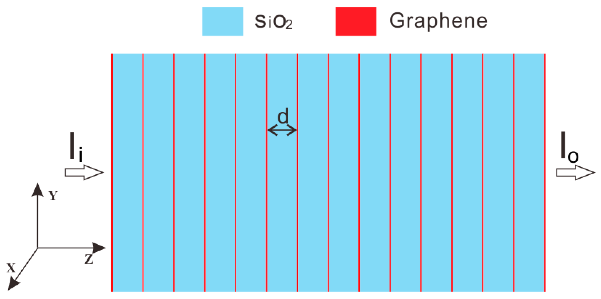
Single sheets of graphene are embedded in silicon dioxide to form arrays of graphene with a fixed spatial period as shown in
Figure 1. Silicon and silicon dioxide are usually used for waveguides or substrate [
29,
30]. In the arrays, the thickness of dielectrics, viz., silicon dioxide, is noted by
d and
N is the period number of graphene. Graphene is an ultrathin two-dimensional material equipped with distinct electrical conductivity. Its surface conductivity is governed by the Kubo formula [
1,
31]:
where
fd = 1/(1 + exp[(
ε −
μc)/(
kBT)]) is the Fermi-Dirac statistical distribution,
kB denotes the Boltzmann constant,
τ is the momentum delay time,
i is the unit of imaginary number,
ε denotes the particle energy,
μc represents the chemical potential of graphene (also known as the Fermi level
EF), and
T is the temperature,
e is the unit charge of electron. The first term of Equation (1) represents the intraband electron-photon scattering process, which can be obtained after integration.
The second term of Equation (1) represents the interband transition of electrons. For
ħω, |
μc| ≫
kBT, it can be simplified as
The energy band of intrinsic graphene is provided in
Figure 2a. Graphene exhibits strong broadband absorption which is 50 times higher than GaAs. For graphene, its surface conductivity is contributed by interband and intraband transitions, which are related to the frequency of photons and the chemical potential on graphene
μc =
EF. The chemical potential of doped graphene can be controlled by chemical doping or external gate voltage [
32]. For intrinsic graphene
EF = 0, there is only interband transition and no intraband contribution.
Figure 2b gives the transitions of electrons in graphene for
EF > 0. The Fermi level is elevated as a negative gate voltage bias on graphene. The effect of this operation is similar to the case of
n-doping. Interband transition only occurs as the incident photon satisfies the condition
ħω1 > 2|
EF|, so the low-wavelength dynamic surface conductivity is dominated by interband contribution. In the THz band, the energy of the photon is relatively low. Interband transition dominates for
ħω2 < 2|
EF| and the conductivity of graphene is approximately in the form of a Drude model, similar to that of the metals. As the graphene is biased by a positive gate voltage, similar to the case of
p-doped, the Fermi level degrades
EF < 0 as shown in
Figure 2c. Interband transition occurs above the threshold of
ħω1 > 2|
EF| as well.
Graphene could be viewed as an equivalent dielectric and numerous simulations have shown that the deviations caused by such emulating can be negligible as long as the equivalent thickness is less than 1 nm [
33,
34].
As a transverse wave is incident in the arrays of graphene from the left and its intensity is low enough, the third-order nonlinear effect in graphene can be ignored. The symbol
Io represents the transmitted intensity of light and
Ii is the intensity incident light wave. The linear transmittance and reflectivity of graphene arrays are derived by the forward transmission matrix method (FTMM) [
1,
35]. However, the nonlinear effect of graphene cannot be ignored as the incident light is strong enough. Then, we can utilize the inverse transmission matrix method (ITMM) [
36] to simulate the nonlinear transmittance in the graphene arrays and the input-output intensity relationship of light.
The nonlinear conductivity coefficient of graphene is denoted by
where
VF ≈
c/300 is the Fermi velocity [
1,
20]. We divide the dielectric into numerous sublayers and calculate the incident light intensity of each sublayer in reverse through the transmission matrix for different output light intensity. For graphene, the nonlinear modification to the surface conductivity of graphene is carried out by using the relationship between the surface conductivity and local intensity of electric field. Then, the complete form of surface conductivity is noted by
Since graphene is regarded as a dielectric with a certain thickness, its equivalent dielectric constant is expressed as
where Δ is the equivalent thickness of graphene, the vacuum resistivity is noted by
η0 and
k0 represents the incidence wave number in vacuum. Here, we collectively give the parameters as follows: the environment temperature
T = 300 K, the equivalent thickness Δ = 0.3 nm, the thickness of each layer of SiO
2 is
d = 10 nm, the period number of graphene arrays is
N = 40, the dielectric constant of silicon dioxide is
ε = 2.1.
3. Optical Bistability, Tristability and Multistability
The reflectivity and transmittance are given in
Figure 3a as a light impinges upon the arrays of graphene. One can see that there is an upward saltus step on the transmission curve. As the input wavelength is lower than 1.25 μm, the transmittance
T fluctuates around 0.5. While the wavelength is greater than 1.25 μm, the transmittance approximates to 1 and fluctuates around this value. There are many peaks in transmission spectrum and these maxima in the curve correspond to resonant states. In addition, the reflectivity
R is low and fluctuates around zero, indicating that most energy of light has been transmitted. The peaks of transmittance face to the zero points of reflectivity exactly. Interband transition of electrons dominates as a short wavelength is incident in the graphene sheets, inducing large loss in intensity of light wave, while the incident wave with long wavelength mainly triggers intraband transition.
As the intensity of incident light is strong enough, so that the third-order nonlinear modification to the surface conductivity of graphene reaches the order of linear counterpart, the influence of light intensity on the transmittance and output intensity of light should be considered. For a fixed incident wavelength,
Figure 3b provides the relationship between transmittance and the intensity of incident light. It can be seen that the transmittance oscillates as the input light intensity increases. In addition, the amplitude of oscillation enlarges gradually. Furthermore, with the increase in intensity of incident light, the negative slope of transmittance curve appears, indicating that optical bistability may be achieved.
Considering the nonlinear effect, the intensity of transmitted light increases with the incident intensity.
Figure 3c provides the input-output relationship. Characteristics of this curve manifest so that it is similar to the hysteresis. By increasing the incident intensity of light, the output intensity makes an abruptly upward jump at
Iu, and the input-output curve varies along path I, while the output light intensity has a downward jump at
Id as the incident intensity declines, and the input-output curve goes along path II. So
Iu is known as the upper threshold, and
Id is defined as the lower threshold. Therefore, for the fixed incident intensity between the values of
Id <
Ii <
Iu, it corresponds to two stable resonant states
S1 and
S2. In general, the output–input intensity relation evolves along path I by increasing the light intensity, while it evolves along path II by decreasing the light intensity. The curve actually corresponds to a double valued function, similar to the hysteresis loop. The two paths represent different physical meanings and here we put them together in the same schematic to make a sharp contrast.
Figure 4a shows the transmission spectra for three different external voltages on graphene. The value of chemical potential depends on the external voltages biased on graphene. The incident wavelength at the saltus step point of transmittance has a red shift as the chemical potential increases. The Fermi level, i.e., the chemical potential, is a critical value to characterize intraband and interband transitions in the energy band. Therefore, the critical incident wavelength triggering the intraband transition decreases as the external voltage on graphene rises.
For different chemical potentials,
Figure 4b displays their corresponding reflection spectra. One can see that the peaks in reflection spectra are just at the valleys in transmission spectra for a given chemical potential, that is, the maximum transmittance is the conjugate of the minimum reflectivity. For a shorter incident wavelength, interband transitions of electrons in graphene are dominant and graphene can be viewed as metals, so the loss of graphene is greater, and the transmittance is lower. As the incident wavelength increases, intraband transition dominates and the loss of light in graphene decreases. Meanwhile, most of the light has been transmitted. Interband transition only occurs as the incident photon satisfies the condition
ħω1 > 2|
EF|. The electrons emitted by interband transition lead to considerable loss of light. Therefore, with the increasing of the chemical potential, the lower limit of frequency of photons required for interband transition increases, which results in a shift in the
R and
T curves towards lower wavelengths, which could be utilized to modulate the reflectivity and transmittivity of light.
The third-order nonlinearity, known as Kerr effect, needs to be considered as the incident intensity of light is strong enough. The transmittance, therefore, may change with the input intensity of light as a strong laser impinges.
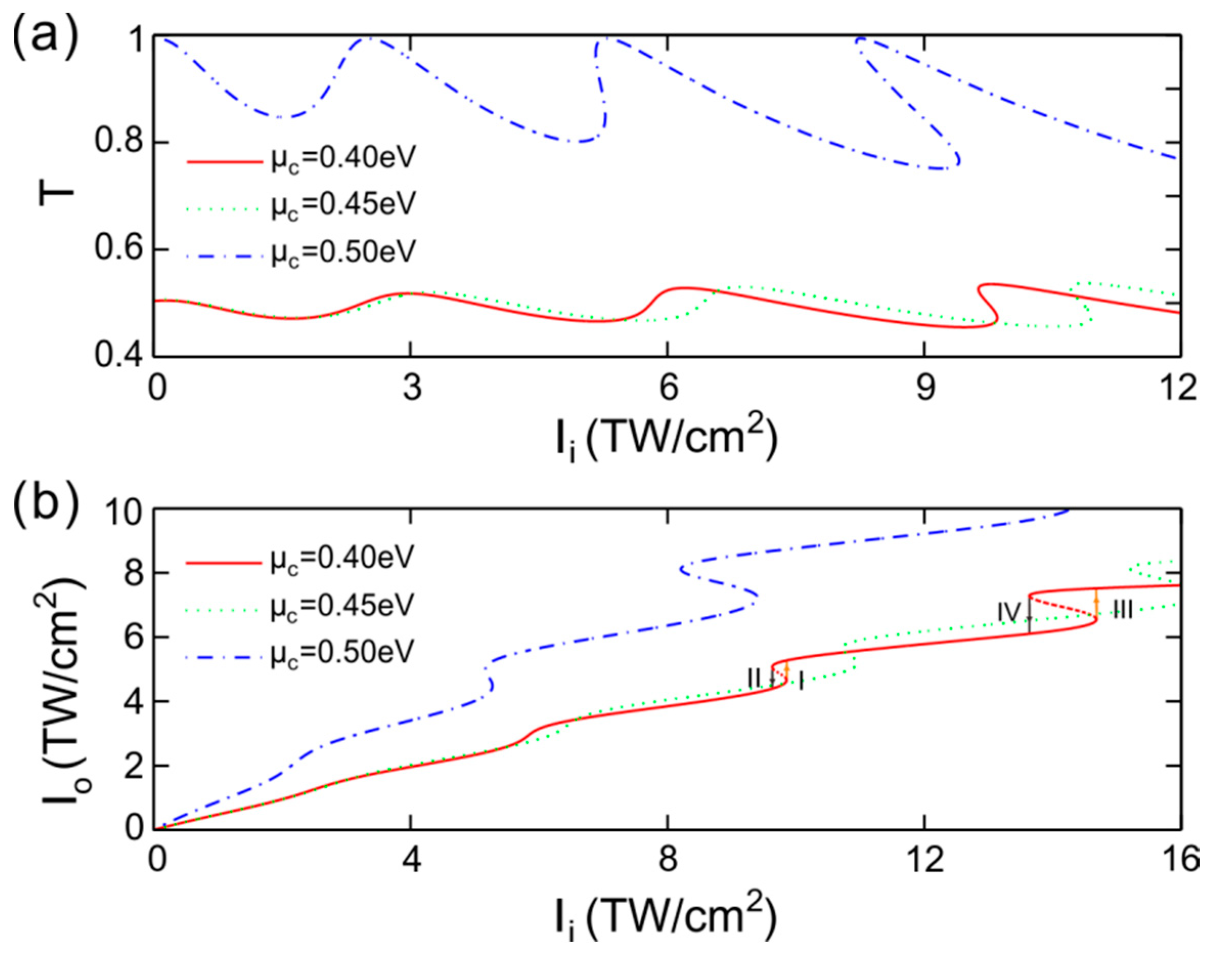
Figure 5a gives the nonlinear transmittance for different values of chemical potential. One can see that, for a given incident intensity, the nonlinear transmittance for
μc = 0.40 eV is larger than those for
μc = 0.45 and 0.50 eV. This characteristic results from the fact that the linear transmittance for the chemical potential, 0.40 eV, is significantly higher than the two others. With the same incident intensity of light, larger nonlinear transmittance results in stronger transmitted intensity.
The negative value in the curve slope of the nonlinear transmittance indicates that optical bistability may be realized if given an appropriate incident intensity.
Figure 5b provides the input–output relationship for different chemical potentials. It can be seen that, for
μc = 0.40 eV, two bistablities appear in the curve within a given input intensity interval. As the intensity of incident light increases, there are two upward jumps, namely I and III, while the incident light intensity decreases, there are two downward jumps, namely II and IV. This specialty can be applied to polymorphic switches. The upper and lower thresholds of bistability can be tuned by an external voltage on graphene.
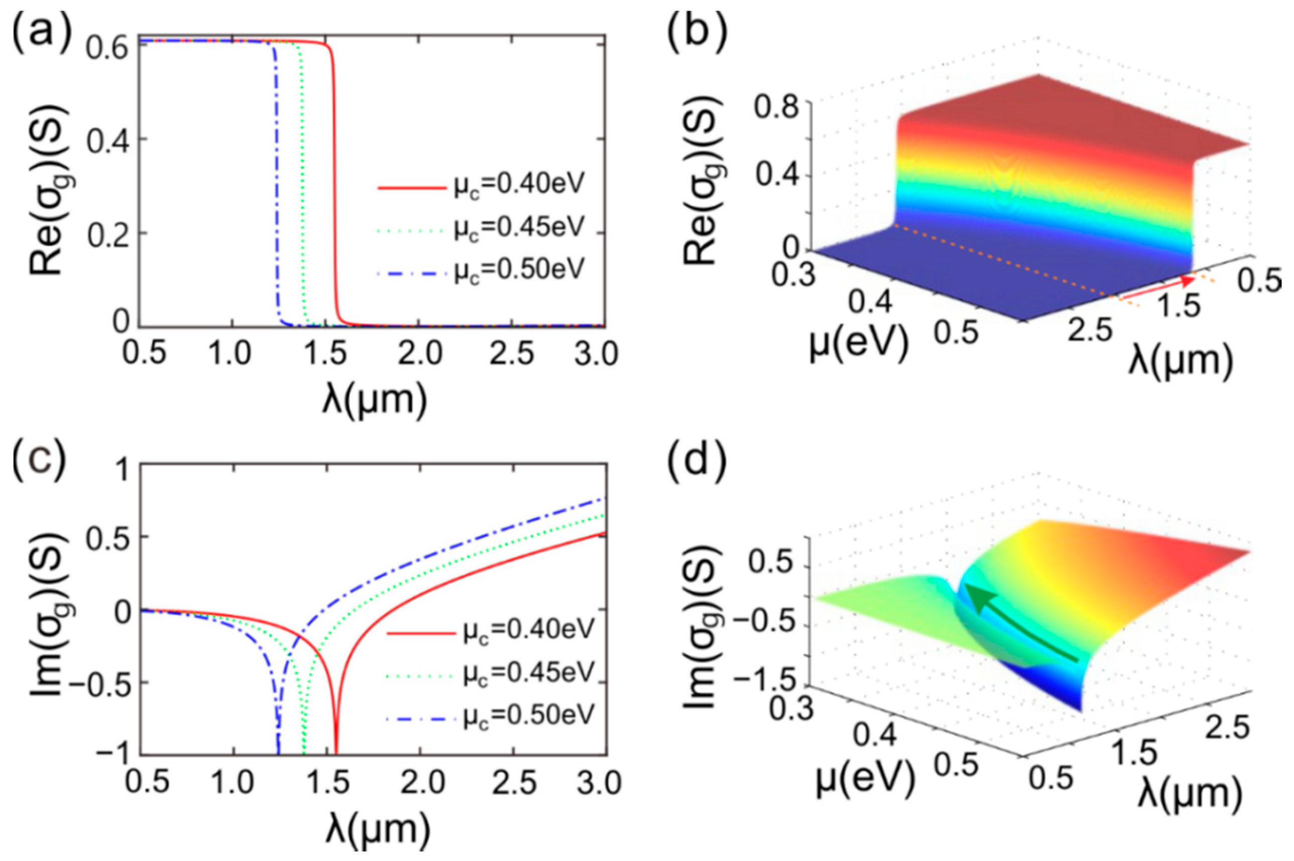
In order to explore the mechanism of formation of these jumps in the transmission spectra, we here investigate the relation between the incident wavelength and the linear surface conductivity of graphene. For three given different chemical potentials
μc = 0.40, 0.45 and 0.50 eV,
Figure 6a gives the real part Re(
σg) of the surface conductivity of graphene. For shorter incident wavelengths, Re(
σg) approximates to 6 S and keeps constant as the wavelength increases. Otherwise, Re(
σg) suddenly jumps downward as the wavelength is continuing to increase. The real value always is as low as zero by increasing the wavelength sequentially. We here have viewed graphene as a dielectric with an equivalent thickness, so the imaginary part in the refraction index of graphene is the counterpart of Re(
σg) representing loss or gain of materials. Therefore, larger Re(
σg) means greater loss and weaker transmitted intensity.
Figure 6b provides the real part of surface conductivity
σg in the parameter space. The chemical potential
μc in graphene and the incident wavelength compose of the parameter space. It shows that there is a waterfall in Re(
σg) as the wavelength and the surface conductivity change. The incident wavelength is
λ = 2.066 μm at the saltus step point in the surface conductivity for
μc = 0.30 eV, while the wavelength at the saltus step point is
λ = 2.066 μm for
μc = 0.55 eV. Therefore, the incident wavelength at these points of dramatic change in the surface conductivity is blueshifted as
μc increases, indicated by the red arrow. The chemical potential can be regulated by an external voltage on graphene. On the other hand, the transmit phase of wave in the arrays of graphene sheets, which can affect transmittance of light, is a function of the surface conductivity. Therefore, the transmittance of light can be flexibly regulated by an external voltage.
The imaginary part Im(
σg) of the surface conductivity represents the real part of the refraction index of graphene. For three given different values of chemical potential,
Figure 6c demonstrates Im(
σg) varying with the incident wavelength. There is a sink in each curve and the sink has a blue shift as
μc increases. However, this obvious feature has a very limited effect on the transmittance due to graphene being ultrathin. It may significantly disturb the complex phase of reflection coefficient.
Figure 6d describes the imaginary part of surface conductivity in the parametric space composed of the chemical potential and incident wavelength. There is a groove in the schematic of Im(
σg) indicated by the arrow. That means the incident wavelength at the valley of Im(
σg) is redshifted as the chemical potential decreases. Drastic changes in the real index of refraction of equivalent dielectric of graphene have only a slight effect on the transmittance.
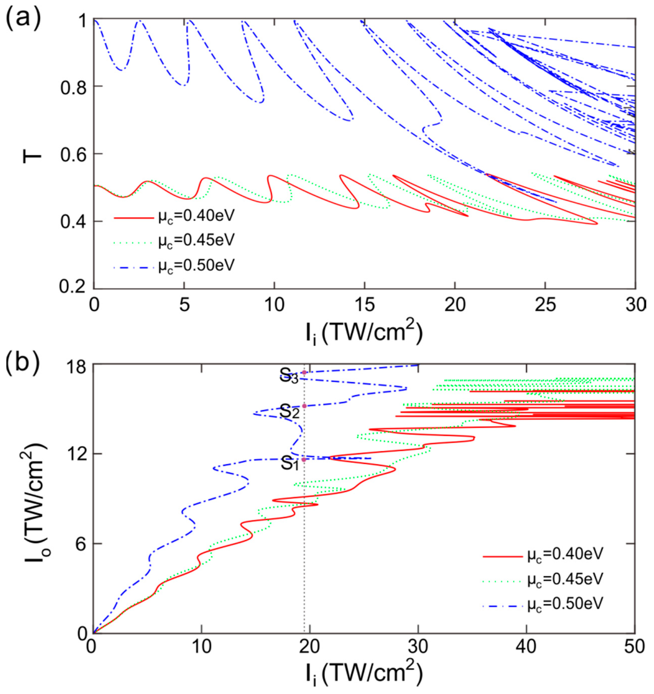
If we keep on increasing the incident light intensity, a settled input intensity of light can correspond to several transmittances with a positive slope as shown in
Figure 7a. This phenomenon indicates that tristability or multistability could be induced in the input-output relationship as the incident intensity is strong enough. In addition, the nonlinear transmittance may overlap for a stronger incident intensity of light. For the incident wavelength
λ = 1.308 μm, we can see that the linear transmittance is larger at 0.5 eV than that at 0.40 or 0.45 eV in
Figure 4a. Interband transition dominates for
ħω1 < 2|
EF|, so the chemical potential affects electron transition in graphene. The nonlinear part of the equivalent refractive index of graphene is proportional to the incident intensity of light. A change in refractive index induces phase shifts of the transmission coefficient in the arrays of graphene sheets. Therefore, the transmittance varies with the incident intensity and the influence of incident intensity on the transmittance is more obvious for a stronger incident intensity of light.
Figure 7b provides optical tristability and multistability for different values of chemical potential. For
μc = 0.50 eV, one can see that the vertical dotted line intersects the input-output curve at three points, i.e.,
S1,
S2 and
S3. This illustrates that for one input there can be three stable outputs, known as optical tristability. As light intensity keeps on increasing, multiple outputs appear for each input, which is known as optical multistability. Optical tristability and multistability may be applied to multivalued all-optical switches or optical storage, respectively. The thresholds and intervals between thresholds of optical tristability and multistability can also be modulated by the external voltage on graphene.


