Article

Contribution to the Physical Modelling of Single Charged Defects Causing the Random Telegraph Noise in Junctionless FinFET

by
Atabek E. Atamuratov
1,*,
Mahkam M. Khalilloev
1,
Ahmed Yusupov
2,
A. J. García-Loureiro
3,
Jean Chamberlain Chedjou
4 and
Kyamakya Kyandoghere
4
1
Department of Physics, Urgench State University, Kh.Olimjan str.,14, 220100 Urgench, Uzbekistan
2
Department of Electronics, Tashkent University of Information Technologies, A.Temur str.,108, 100200 Tashkent, Uzbekistan
3
Department of Computational electronics, University of Santiago de Compostela, Praza do Obradoiro, 15782 Santiago de Compostela, Spain
4
Department of Transportation informatics, University of Klagenfurt, 9020 Klagenfurt, Austria
*
Author to whom correspondence should be addressed.
Appl. Sci. 2020, 10(15), 5327; https://doi.org/10.3390/app10155327
Submission received: 12 July 2020 / Revised: 28 July 2020 / Accepted: 29 July 2020 / Published: 1 August 2020
(This article belongs to the Special Issue Device Modeling for TCAD and Circuit Simulation)

Abstract

:
In this paper, different physical models of single trap defects are considered, which are localized in the oxide layer or at the oxide–semiconductor interface of field effect transistors. The influence of these defects with different sizes and shapes on the amplitude of the random telegraph noise (RTN) in Junctionless Fin Field Effect Transistor (FinFET) is modelled and simulated. The RTN amplitude dependence on the number of single charges trapped in a single defect is modelled and simulated too. It is found out that the RTN amplitude in the Junctionless FinFET does not depend on the shape, nor on the size of the single defect area. However, the RTN amplitude in the subthreshold region does considerably depend on the number of single charges trapped in the defect.

1. Introduction

Decreasing the critical metal-oxide-semiconductor field effect transistor (MOSFET) dimensions up to the nanometer-scale induces the increasing of the defect influence on carrier mobility, subthreshold swing, and threshold voltage. It also stimulates both instability and degradation of the transistor in active mode. Depending on certain conditions and the type of measurements, the instability may be responsible for bias temperature instability (BTI), random telegraph noise (RTN), and a hysteresis of characteristics [1]. Especially amongst these effects, a single interface or oxide defect on the drain current can be noticed. These single charged traps can induce instability in the operation of the transistor [2], generate RTN in the MOSFET and affect both stability and reliability of MOSFET-based circuits [3,4]. On the other hand, RTN can be used as a tool for analyzing and exploring the defect behavior of the oxide–semiconductor interface of the MOSFET [5,6].
Therefore, it is very important to investigate a single interface or the influence of an oxide charged trap on the characteristics of the MOSFET. One of the reliable simulation methods for studying such defects is the so-called atomistic approach [7]. However, this technique requires a magnificent effort in computation (in terms of time and memory), particularly while simulating integrated circuits on a MOSFET basis. Therefore, the development of a simple physical model of the single-trapped charge useable in commercial widely used Technology Computer Added Design (TCAD) programs is an important task from the point of view of significantly reducing the computational time required for these types of simulation studies. The model should properly describe the processes related to the trapped charge influence on the charge transfer processes in these devices. The TCAD Sentaurus provides the opportunity of simulating the charge trapping in the oxide layer or at the interface in MOSFET (model of traps and fixed charges). However, to fully describe the trapped charge, a clear specification of both the boundary conditions and the density of charge is required. In the literature, usually, the single trapped charge is modeled as simple cell with appropriate boundary conditions [2,8]. However, there is no experimental research work indicating clear criteria for defining appropriate and specific sizes of the cell describing the single trapped charge. The sizes presented in various works differ by several orders of magnitude. Besides, to the best of our knowledge, no research has been carried out addressing the dependency and correlation between the single charge effect, the size and shape of the charged area. Therefore, in this work, the effect of a simple cell model is compared with other proposed models of single trapped charge with appropriate (i.e., using suitable) boundary conditions. The single trapped charge effect/ dependency on the size of the charged area are estimated. One of the important effects of the single trapped charge is generation of the Random Telegraph Noise. Therefore, the RTN amplitude dependency on the size and shape of the charged area is considered.
The influence of a single trapped charge on the noise characteristics has been widely investigated for the planar MOSFETs [9,10,11,12] and FinFETs [13,14], while very few works were devoted to investigating the RTN amplitude in the relatively new Junctionless FinFET [15,16]. Thus, the influence of both shape and size of the single trapped charge to noise characteristics of nanometer Junctionless FinFET is closely studied in this paper.

2. Modeling and Simulation Procedure

Nowadays, there is no universal physical model that describes the spatial distribution and sizes of the single charge trapped at the interface or in the oxide defects in a MOSFET. Moreover, it is very interesting to implement these models in commercial TCAD programs. There are many geometrical sizes, which describe spatial sizes of an elementary component of solid states such as the Bohr radius, Van der Vaals radius or atomic radius. All of the above might be used as a size-related single defect physical model.
We consider that the trap defect at the Si-SiO2 interface or in the oxide is a broken connection between silicon atoms (or between silicon and oxygen atoms). In general, hydrogen atoms are introduced to recover the dangling bonds. However, because it (i.e., the recovery) is a statistical process, some broken bonds may not be recovered by hydrogen atoms. This case is very important in nanometer devices because the charged trap will have a significant impact on the device characteristics.
In some cases, the trap in oxide may be represented by a vacancy V0, which can capture carrier according to the reaction
V0 + e = > V
where e and V denote the elementary charge and charged vacancy, respectively. Hence, the defect will represent a local charged area with some spatial shape. It is expected that the single trapped charge will be distributed in that local area. It can be assumed that the sizes of this area will be restricted by atomic sizes as well as by interatomic distances inherent to the considered materials. Interatomic distances at the interface, as well as in bulk, vary depending on defect’s position and layer’s thickness. Thus, the distance between silicon and oxygen atoms RSi-O varies in the range from 0.154 nm to 0.162 nm, and the distance between neighboring oxygen atoms RO-O ranges between 0.248 and 0.265 nm at changing SiO2 thickness from 0.4 nm to bulk [17] (Figure 1). However, in [18], it is stated that RO-O is equal to 0.227 nm, and the average distance between silicon and oxygen atoms is equal to 0.162 nm in SiO2. Further, it is indicated that the distance between silicon atoms RSi-Si is equal 0.543 in crystal silicon and the atomic radius for silicon RSi and for oxygen RO ranges between 0.118 and 0.065 nm correspondingly. At the transition layer from Si to bulk SiO2, the ratio of the number of silicon and oxygen atoms is changed depending on the position. Therefore, the atomic distances indicated above, and, as a consequence, the interface defect sizes, can change in some range.
When decreasing the transistor dimensions to decrease the tunneling current through the gate oxide, HfO2 with a high dielectric constant and the appropriate equivalent thickness is mainly used instead of SiO2. Therefore, it is also interesting to notice the characteristic interatomic distances in this material. Depending on orientation and number of atomic layers from 3 to 11, the distances between oxygen atoms vary from 0.254 up to 0.265 nm. In addition, the distances between Hf and oxygen atoms vary from 0.202 nm up to 0.248 nm [19] (see Figure 2). In the transition layer Si-HfO2, the average distance between Si and Hf atoms is 0.260 nm [20]. In this transition layer, the break of the connections between silicon atoms as well as the oxygen vacancies is responsible for the arising of the interface defects [21]. Due to the facts indicated above, it is obvious that the interatomic distances and, as a consequence, the trap defect linear sizes are in accordance with the ranges indicated above. In some papers, the trap sizes are considered in the electron (or hole) capture cross-section point of view. For the considered materials, often, the range of the capture cross sections is taken from 10−18 up to 10−13 cm2 [22,23,24]. This range of the cross section fits to the range of the linear sizes of defects from 1.8 nm up to 0.005 nm and it covers the range of possible defect sizes indicated above. It can be summarized that for the substrate and oxide materials used for MOSFET, the typical atomic linear sizes and interatomic distances are in the range between 0.05 and 0.55 nm.
However, these above described sizes do not allow for arguing the defect’s shape and/or assessing the spatial distribution of single trapped charge in the defect. The spatial distribution of the single charge in the trap is described by the wave function of the carrier in the defect. The wave function depends on the excitation condition of the defect. Obviously, in the basic non-excited state, the charge distribution can be modeled by a simple homogeneously charged sphere with the center allocated in the defect’s center (see Figure 3, form (a)). For comparison, the idealized forms of the charge distribution, which would be appropriate to the wave function of the excited condition, are considered too (Figure 3, forms (b) and (c)). In many papers studying the influence of a single charged trap on the characteristics of the MOSFET, the charged area is considered as a homogeneously charged simple cell [3,8]. Therefore, for comparison, besides the forms indicated above, the single defect model in the form of a simple cell is also considered (see Figure 3, form (d)).
Our analysis is mainly based on the McWhorter model of RTN and we have considered only the steady state, but not dynamic features [25,26,27]. We have considered the influence of the size and shape of the defect area on the amplitude of the RTN in a Junctionless MOSFET. For this purpose, the RTN amplitude dependence on the gate voltage overload (Vg – Vth) is simulated by trapping the single defect with different sizes and forms at the interface, as well as in the oxide layer.
The spherical model of a single trapped charge is considered for the first time. It is therefore necessary to check whether this model is appropriate. In this context, we first compared the RTN simulation results induced by this model with the experimental results of a classic planar MOSFET, which were discussed in detail in [27]. The proposed physical model of the defect, and the transport model for the RTN simulation, are all calibrated by using experimental results. To calibrate the models, one considers the planar MOSFET structure with the same parameters as for the experimental sample [27], and for the model of the single defects, a sphere with radius r = 0.13 nm homogeneously charged by elementary charge (see Figure 3, form (a)) is used. Experiments carried out in [27] utilize silicon oxynitride (SiON) n-channel MOSFET devices with a physical dielectric thickness of 1.4 nm. The nominal channel widths are in the range 0.085 µm to 1 µm and the nominal channel lengths are between 0.055 µm and 1 µm. A full description of the RTN measurement apparatus and methods can be found in [27]. Indeed, source and gate electrodes are biased using battery-powered variable-voltage sources, while the substrate electrode is grounded for all measurements. The drain current is monitored by a low-noise current amplifier with 2 kHz bandwidth. The amplifier output is directly captured using a digital storage oscilloscope with a large memory depth (107 Samples). The experimental measurements (obtained in the form of time series data) are further analyzed offline. The parameters of the simulated transistor are shown in Table 1. In the simulation, SiON is used for gate oxide; the same is done in the experimental sample.
The simulation and experimental results for a MOSFET with widths 90 and 130 nm are shown and compared in Figure 4. Regarding the RTN amplitude, it is seen that the simulation values are sufficiently close to the experimental ones when the gate overload lies in the range between −0.15 and 0.1 V for both gate widths. The RTN amplitude differences observed between simulation and experimental results outside of the previously specified range, obviously, are due to fluctuations in the experimental samples’ parameters responsible for the drain current. This is confirmed by the significant differences observed in the RTN amplitude for two different experimental samples outside of the indicated range: the jumping increase is observed for the positive gate overload higher than 0.1 V for the sample with width 130 nm, and for the negative gate overload lower than 0.15 V for the sample with a width of 90 nm.
Reasonable agreement with the experimental results enables the use of this model in Junctionless FinFET and comparison with various other models, especially the conventional simple cell model. The proposed defect model was applied for simulating the RTN amplitude generated by single charges trapped at the oxide–semiconductor interface, as well as in the gate oxide layer of nanosized Junctionless (JL) Silicon on Insulator (SOI) FinFET. The RTN amplitude was calculated in steady state condition using the following expression
RTN = (│Id0 − Id │)/Id0
where Id0 and Id denote the drain current before and after trapping the single charge, respectively. The structure of the simulated transistor is shown in Figure 5a and the corresponding parameters are presented in Table 2.
3D simulations were performed in the framework by a drift-diffusion model using the TCAD Sentaurus software. The influence of trapped charge in this model is accounted by trapped charge density ρtrap in the Poisson equation, which is part of the transport model used [28]:
∇ε∇φ = − q(pn + ND − NA ) − ρytap
where ε is the electrical permittivity, q is the elementary electronic charge, n and p are the electron and hole densities, ND is the concentration of ionized donors, NA is the concentration of ionized acceptors. Boundary conditions for ρtrap are determined by the form of charged defect (Figure 3). In Sentaurus, an area with a certain shape, size, and boundary was created in the oxide layer and at the boundary using the Sentaurus Structure Editor, which corresponds to the different single trapped charge models at stake (i.e., under consideration). In the “Physics” section of the Sentaurus Device, the parameters of a charge trap were defined for various models at stake (i.e., under consideration). The used transport model considered the influence of the doping level on the carrier mobility, the saturation of carrier velocity, and the influence of the normal field component on the drain current. Since the transistor had nanoscale dimensions, it was also necessary to take into account the quantum confinement effects. The present work employed quantum corrections with respect to the density gradient, which is preferred in the framework of drift-diffusion simulations [29,30]. The adopted transport model has been calibrated on experimental Id–Vg characteristics carried out in [31]. The experimental transistor preparation and measurements details are described in [31]. According to this work, [110]-trigate nanowires with high-κ/metal gate stack were fabricated on (100) SOI wafers with a 12 nm top silicon layer and a buried oxide thickness of 145 nm. The SOI layer was thinned down to 10 nm. The silicon layer is patterned to create nanowires by using a mesa isolation technique. The gate stack consists of 2.3 nm CVD HfSiON, 5 nm ALD TiN, and polysilicon (50 nm) layers (equivalent oxide thickness (EOT) ≈ 1.2 nm). As for the active patterning, photoresist trimming is used to address gate lengths up to 13 nm.
The comparison of Id–Vg characteristics obtained from both simulation and experiment is shown in Figure 5b. A good calibration between simulation and experimental characteristics in the subthreshold as well as in the superthreshold regions was obtained. Hereby, the trap at the interface of the defect area is modeled by the projection of the spatial defect to the interface surface with an appropriate density of charge.
For an adequate comparison of the effect of different defect forms, the volume of different spatial defect forms as well as the area of different forms of interface defects were correspondingly chosen to be equal. The radius of the spherical model of the defect in the oxide layer and that of the circle model at the interface surface were chosen to equal 0.15 nm.

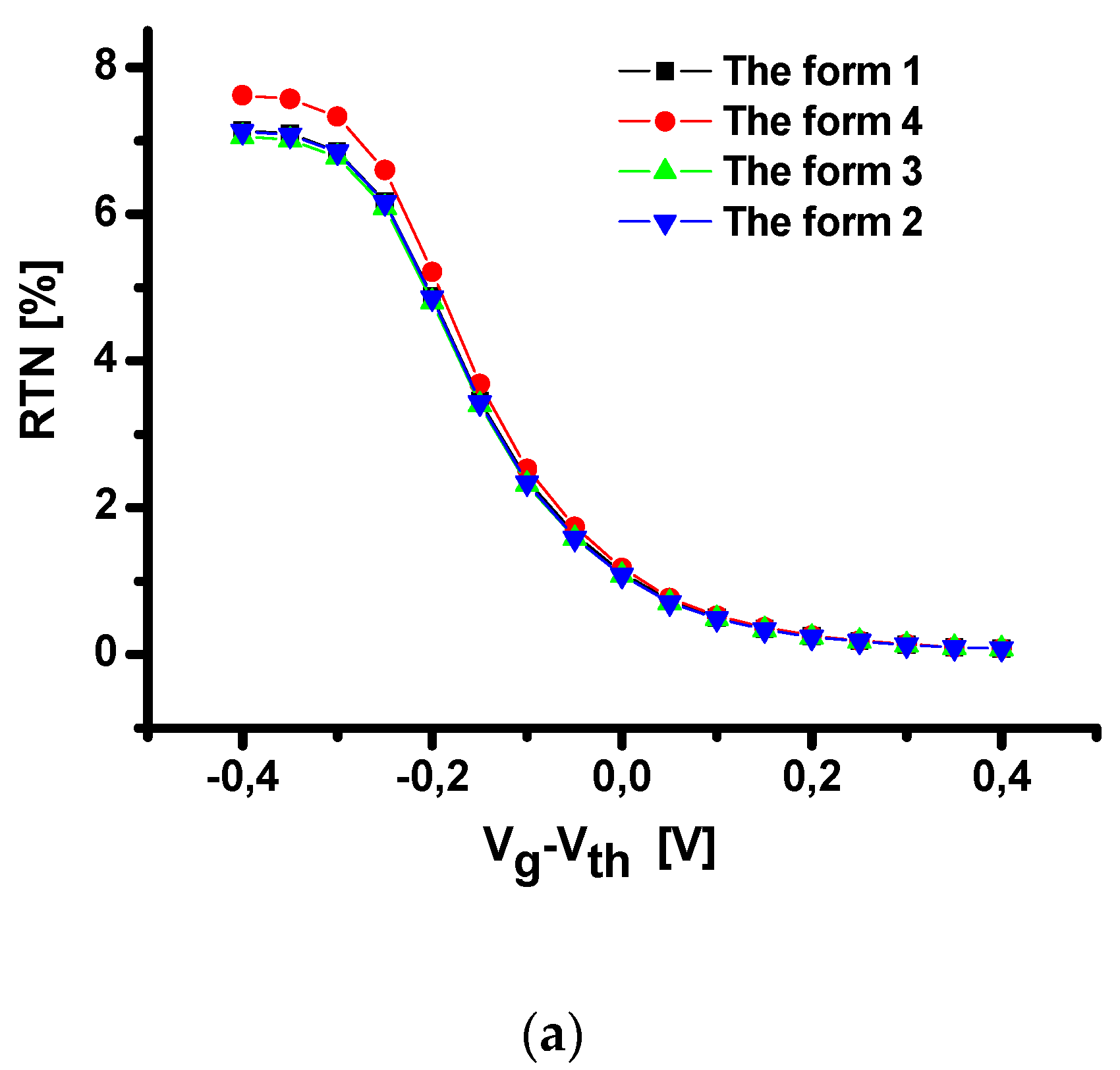
3. Simulation Results and Discussions

The simulation results of the RTN amplitude dependence on gate voltage at single charge trapping in the oxide layer and at the interface are shown in Figure 6. It is seen that for both single oxide and interface defects, the RTN amplitude dependence on the gate voltage overload is not influenced by the considered form of the single defect. Figure 6 also indicates that a single defect trap in the oxide layer can be modeled by a homogeneously charged sphere (or circle at the interface) or by a simple cell.
The RTN amplitude dependence on the radius of spherical or circular area of defects in the oxide or at the interface, correspondingly, was simulated to study the influence of the defect size.
One has considered the radius range between 0.1 and 0.5 nm, which covers practically all featured linear sizes of atomic radius and interatomic distances in Si, SiO2, and HfO2. When changing the radius only, the charge density is modified because the trapped charge remains single and elementary. The results show that the RTN amplitude depends linearly, but very weakly, on the radius of the defect and practically does not change in the radius range under consideration (see Figure 7). When increasing the radius of the defect area, at a constant trapped charge, the RTN amplitude is practically not changed in all considered ranges of the gate voltage overload. The RTN amplitude in the subthreshold region is not as high as it is reported in some experimental works [14,25]. To find out a possible reason for creating the large RTN amplitudes in the subthreshold region, as observed in our experiments, we have studied the RTN amplitude dependence on single charge quantity in the spherical defect area at the constant radius 0.15 nm. We considered the repeatedly charged defect with constant size. In this case, the RTN is appreciably changed in the subthreshold as well as in the near-threshold region (see Figure 8, Figure 9a). The RTN amplitude in the subthreshold region is considerably increased when increasing the number of single charges N in the defect (see Figure 9b). Obviously, the main reason for creating the high RTN amplitude is not the size as well as the shape of the defects but the density or the number of trapped charges in the defect.

4. Conclusions

We have found out that the RTN amplitude in a Junctionless FinFET does not actually depend on the single charge spatial distribution in the defect. A simplified simulation of the single trap can be modeled by the homogeneously charged simple cells in both the oxide and interface trap cases. Moreover, the RTN amplitude does not practically depend on the linear size of the charged area in the range from 0.1 up to 0.5 nm. However, the RTN amplitude is considerably increased with the increasing number of single charges trapped in the defect. In particular, a high amplitude is created at the subthreshold region, depending on the number of the trapped charge.

Author Contributions

Conceptualization, A.E.A., A.Y.; methodology, A.E.A., M.M.K.; software, M.M.K.; validation, A.E.A. and M.M.K.; formal analysis, A.J.G.-L.; investigation, M.M.K.; resources, M.M.K.; data curation, M.M.K.; writing—original draft preparation, A.E.A.; writing—review and editing, K.K. and J.C.C.; visualization, J.C.C., K.K. and A.Y.; supervision, K.K.; project administration A.E.A.; funding acquisition, A.E.A. All authors have read and agreed to the published version of the manuscript.

Funding

This research was funded by Ministry of Innovation Development of the Republic of Uzbekistan, grant number OT-F2-67.

Conflicts of Interest

The authors declare no conflict of interest.

References

  1. Kaczer, B.; Franco, J.; Weckx, P.; Roussel, P.J.; Putcha, V.; Bury, E.; Simicic, M.; Chasin, A.; Linten, D.; Parvais, B.; et al. A brief overview of gate oxide defect properties and their relation to MOSFET instabilities and device and circuit time-dependent variability. Microelectron. Reliab. 2018, 81, 186–194. [Google Scholar] [CrossRef]
  2. Kang, C.J.; Buh, G.H.; Lee, S.; Kim, C.K.; Mang, K.M.; Im, C.; Kuka, Y. Charge trap dynamics in a SiO2 layer on Si by scanning capacitance Microscopy. Appl. Phys. Lett. 1999, 74, 1815–1817. [Google Scholar] [CrossRef]
  3. Sriram, S.R.; Bindu, B. Analytical modeling of random discrete traps induced threshold voltage fluctuations in double-gate MOSFET with HfO2/SiO2 gate dielectric stack. Microelectron. Reliab. 2019, 99, 87–95. [Google Scholar]
  4. Toh, S.O.; Liu, T.J.K.; Nikolic, B. Impact of Random Telegraph Signaling Noise on SRAM Stability. In Proceedings of the 2011 Symposium on VLSI Technology—Digest of Technical Papers, Honolulu, HI, USA, 14–16 June 2011; pp. 204–205. [Google Scholar]
  5. Kao, T.H.; Chang, S.J.; Fang, Y.K.; Huang, P.C.; Wang, B.C.; Wu, C.Y.; Wu, S.L. Investigation of low-frequency noise of 28-nm technology process, of high-k/metal gate p-MOSFETs with fluorine incorporation. Solid-State Electron. 2016, 115, 7–11. [Google Scholar] [CrossRef]
  6. Javier, D.; Javier, M.; Rosana, R.; Rafael, C.; Elisenda, R.; Francisco, V.; Fernandez, M.N. A smart noise- and RTN-removal method for parameter extraction of CMOS aging compact models. Solid-State Electron. 2019, 159, 99–105. [Google Scholar]
  7. Asenov, A.; Balasubramaniam, R.; Brown, A.R.; Davies, J.H.; Saini, S. Random Telegraph Signal Amplitudes in Sub-100 nm (Decanano) MOSFETs: A 3D “Atomistic” Simulation Study. In Proceedings of the International Electron Devices Meeting, San Francisco, CA, USA, 10–13 December 2000; pp. 279–282. [Google Scholar]
  8. Velayudhan, V.; Gamiz, F.; Martin-Martinez, J.; Rodriguez, R.; Nafria, M.; Aymerich, X. Influence of the interface trap location on the performance and variability of ultra-scaled MOSFETs. Microelectron. Reliab. 2013, 53, 1243–1246. [Google Scholar] [CrossRef]
  9. Contoyiannis, Y.; Potirakis, S.M.; Stavrinides, S.G.; Hanias, M.P.; Tassis, D.; Theodorou, C.G. Intermittency-induced criticality in the random telegraph noise of nanoscale UTBB FD-SOI MOSFETs. Microelectron. Eng. 2019, 216, 111027. [Google Scholar] [CrossRef]
  10. Shamsur, A.S.M.; Rouf, Z.Ç. Channel hot carrier induced volatile oxide traps responsible for random telegraph signals in submicron pMOSFETs. Solid-State Electron. 2020, 164, 107745. [Google Scholar] [CrossRef]
  11. Carlos, M.; Noel, R.; Francisco, G.; Akiko, O. Systematic method for electrical characterization of random telegraph noise in MOSFETs. Solid-State Electron. 2017, 128, 115–120. [Google Scholar]
  12. Angelica, L.; Andrew, R.; Brown, A.A.; Scott, R. Random telegraph signal noise simulation of decanano MOSFETs subject to atomic scale structure variation. Superlattices Microstruct. 2003, 34, 293–300. [Google Scholar]
  13. Gerrer, L.; Amoroso, S.M.; Hussin, R.; Asenov, A. RTN distribution comparison for bulk, FDSOI and FinFETs devices. Microelectron. Reliab. 2014, 54, 1749–1752. [Google Scholar] [CrossRef]
  14. Fan, M.L.; Yang, S.Y.; Hu, V.P.H.; Chen, Y.N.; Su, P.; Chuang, C.T. Single-trap-induced random telegraph noise for FinFET, Si/Ge Nanowire FET, Tunnel FET, SRAM and logic circuits. Microelectron. Reliab. 2014, 54, 698–711. [Google Scholar] [CrossRef]
  15. Rudenko, T.; Nazarov, A.; Barraud, S.; Kilchytska, V.; Flandre, D. A method for threshold voltage extraction in junctionless MOSFETs using the derivative of transconductance-to-current ratio. Solid-State Electron. 2019, 161, 107723. [Google Scholar] [CrossRef]
  16. Lee, C.W.; Ferain, I.; Afzalian, A.; Yan, R.; Akhavan, N.D.; Razavi, P.; Colinge, J.P. Performance estimation of junctionless multigate transistors. Solid-State Electron. 2010, 54, 97–103. [Google Scholar] [CrossRef]
  17. Miura, K.; Ino, T.; Tada, M.; Ohsaki, H. Shrinkage of atomic distances in ultrathin a-SiO2 film. Philos. Mag. 1992, 66, 25–36. [Google Scholar] [CrossRef]
  18. Hössinger, A. Simulation of Ion Implantation for ULSI Technology. Ph.D. Thesis, Technische Universität Wien, Wien, Austria, July 2000. [Google Scholar]
  19. Beltrán, J.I.; Muñoz, M.C.; Hafner, J. Structural, electronic and magnetic properties of the surfaces of tetragonal and cubic HfO2. New J. Phys. 2008, 10, 063031. [Google Scholar] [CrossRef] [Green Version]
  20. Tang, C.; Ramprasad, R. Oxygen defect accumulation at Si:HfO2 interfaces. Appl. Phys. Lett. 2008, 92, 182908. [Google Scholar] [CrossRef] [Green Version]
  21. Benthem, K.V.; Rashkeev, S.N.; Pennycook, S.J. Atomic and Electronic Structure Investigations of HfO2/SiO2/Si Gate Stacks Using Aberration-Corrected STEM. In AIP Conference Proceedings; American Institute of Physics: College Park, MD, USA, 2005; Volume 788, pp. 79–84. [Google Scholar] [CrossRef]
  22. DiMaria, D.J. The Physics of SiO2 and its Interfaces; Pantelides, S.T., Ed.; Pergamon: New York, NY, USA, 1978; pp. 160–178. [Google Scholar]
  23. Lax, M. Cascade capture of electrons in solids. Phys. Rev. 1960, 119, 1502. [Google Scholar] [CrossRef]
  24. Tzou, J.J.; Sun, J.Y.; Sah, C.T. Field dependence of two large hole capture cross sections in thermal oxide on silicon. Appl. Phys. Lett. 1983, 43, 861. [Google Scholar] [CrossRef]
  25. McWhorter, A.L. 1/f Noise and Germanium Surface Properties. In Semiconductor Surface Physics; Kingston, R.H., Ed.; University of Pennsylvania Press: Philadelphia, PA, USA, 1957; pp. 207–228. [Google Scholar]
  26. Goes, W.; Schanovsky, F.; Grasser, T.; Reisinger, H.; Kaczer, B. Advanced Modeling of Oxide Defects for Random Telegraph Noise. In Proceedings of the 21st International Conference on Noise and Fluctuations, Toronto, ON, Canada, 12–16 June 2011; pp. 204–207. [Google Scholar]
  27. Campbell, J.P.; Yu, L.C.; Cheung, K.P.; Qin, J.; Suehle, J.S.; Oates, A.; Sheng, K. Large Random Telegraph Noise in Sub-Threshold Operation of Nano-Scale nMOSFETs. In Proceedings of the 2009 IEEE International Conference on IC Design and Technology, Austin, TX, USA, 18–20 May 2009; pp. 17–20. [Google Scholar]
  28. Sentaurus™ Device User Guide; Version 2018; Synopsys: Mountain View, CA, USA, 2018.
  29. García-Loureiro, A.J.; Seoane, N.; Aldegunde, M.; Valín, R.; Asenov, A.; Martinez, A.; Kalna, K. Implementation of the density gradient quantum corrections for 3-D simulations of multigate nanoscaled transistors. IEEE Trans. Comput.-Aided Des. Integr. Circuits Syst. 2011, 30, 841. [Google Scholar]
  30. Asenov, A.; Brown, A.; Watling, J. Quantum Corrections in the Simulation of Decanano MOSFETs. Solid-State Electron. 2003, 47, 1141. [Google Scholar] [CrossRef] [Green Version]
  31. Barraud, S.; Berthomé, M.; Coquand, R.; Cassé, M.; Ernst, T.; Samson, M.P.; Perreau, P.; Bourdelle, K.K.; Faynot, O.; Poiroux, T. Scaling of Trigate Junctionless Nanowire MOSFET with Gate Length Down to 13 nm. Electron. Device Lett. 2012, 33, 9. [Google Scholar] [CrossRef]
Figure 1. Model of the crystal lattices of (a) SiO2 and (b) Si.
Applsci 10 05327 g001
Figure 2. Model of the Si-HfO2 structure.
Applsci 10 05327 g002
Figure 3. Models of a single charged defect with different forms of charge distribution. (a) is form of defect in basic state; (b,c) are forms of defect in excited state; (d) is simple cell form of the defect.
Applsci 10 05327 g003
Figure 4. RTN amplitude dependence on the gate overload for the planar MOSFET with gate widths 130 (a) and 90 (b) nm.
Applsci 10 05327 g004
Figure 5. The structure of the simulated JL MOSFET (a) and comparison of Id–Vg characteristics of the transistor carried out from simulation and experiment (b).
Applsci 10 05327 g005
Figure 6. Random telegraph noise (RTN) amplitude dependence on the gate voltage overload generated by single charged defect with different forms: in the oxide layer (a) and at the interface (b).
Applsci 10 05327 g006aApplsci 10 05327 g006b
Figure 7. RTN amplitude dependence on the radius of (a) the oxide, and (b) the interface single charged defects at a constant trapped charge.
Applsci 10 05327 g007
Figure 8. RTN amplitude dependence on the gate overload for different numbers of the single charges trapped N in the defect area.
Applsci 10 05327 g008
Figure 9. RTN amplitude dependence on the number of the single charge trapped in the defect area at gate overload 0 V (a) and −0.4 V (b).
Applsci 10 05327 g009
Table 1. The parameters of the simulated MOSFET.
ParametersDesignationValue of the Parameters
The channel doping concentrationNch2 × 1016 cm−3
Gate oxide thicknesstox1.4 nm
Gate widthWgate90, 130 nm
Gate lengthLgate55 nm
Table 2. Parameters of the simulated SOI FinFET.
ParametersDesignationValue of the Parameters
The channel doping concentrationNch5 × 1018 cm−3
Equivalent gate oxide thickness (HfO2)teff1.2 nm
Channel thicknessTsi9 nm
Channel widthWfin22 nm
Gate widthWgate55 nm
Gate lengthLgate13 nm

