Article

Zinc Oxide Nanorod Surface-Enhanced Raman Scattering Substrates without and with Gold Nanoparticles Fabricated through Pulsed-Laser-Induced Photolysis

1
Division of Pediatric Surgery, Department of Surgery, Taichung Veterans General Hospital, Taichung 40705, Taiwan
2
Department of Medicine, National Yang-Ming University, Taipei 112, Taiwan
3
Department of Applied Materials and Optoelectronic Engineering, National Chi Nan University, Nantou 54561, Taiwan
4
Department of Applied Physics, Faculty of Physics and Engineering Physics, University of Science, Ho Chiç Minh City, Vietnam
5
Department of Electrical Engineering, National Chi Nan University, Nantou 54561, Taiwan
*
Authors to whom correspondence should be addressed.
Appl. Sci. 2020, 10(14), 5015; https://doi.org/10.3390/app10145015
Submission received: 18 June 2020 / Revised: 14 July 2020 / Accepted: 17 July 2020 / Published: 21 July 2020
(This article belongs to the Special Issue Nano-Biophotonics in Sensing Using Nanostructures)

Abstract

:
We fabricated surface-enhanced Raman scattering (SERS) substrates using gold nanoparticle (AuNP)-decorated zinc oxide (ZnO) nanorods (NRs). Prior to decoration with AuNPs, ZnO NRs on the glass substrate fabricated using the sol–gel method could enhance the SERS signal for detecting 10−5 M rhodamine 6G (R6G). Microscopic analysis revealed that the thermal-annealing process for fabricating the seed layers of ZnO facilitated the growth of ZnO NRs with the highly preferred c-axis (002) orientation. A decrease in the diameter of ZnO NRs occurred because of the use of annealed seek layers further increased the surface-to-volume ratio of ZnO NRs, resulting in an increase in the SERS signal for R6G of 10−5 M. To combine the localized surface plasmon resonance (LSPR) mode with the charge transfer (CT) mode, ZnO NRs were decorated with AuNPs through pulsed-laser-induced photolysis (PLIP). However, the preferred vertical (002) orientation of ZnO NRs was prone to the aggregation of AuNPs, which hindered the SERS signal. The experimental results revealed that ZnO NRs with the crystalline structure of horizontal (100) and (101) orientations facilitated the growth of homogeneous, independent and isolated AuNPs which serves as “hot spots” for SERS signal of detecting R6G at a low concentration of 10−9 M. Comparing to previous fabrication of SERS substrate, our method has advantage to fabricate AuNP-decorated ZnO NR in a short time. Moreover, the optimization of the SERS behaviors for different fabrication conditions of AuNPs using the PLIP method was investigated in detail.

1. Introduction

Raman spectroscopy, a spectroscopic analysis based on the inelastic scattering of light (laser as the excited light source) from excited molecules, reveals information on the vibration of functional chemical bonds in molecules and enables reliable identification of unknown species [1]. However, because of the extremely small scattering intensity and persistent problem of photoluminescence of Raman spectroscopy, which increases the background noise and results in a low signal-to-noise ratio. The surface-enhanced Raman scattering (SERS) technique, first observed by Fleischman in 1974 [2], can efficiently enhance the Raman signal through localized surface plasma resonance (LSPR) from metals. When electromagnetic waves travel along the surface of a metal plate with a wave frequency smaller than the plasma frequency of electrons in the metal, the interaction between the wave and the electron clouds amplifies the electric field locally, leading to large-intensity Raman signals [1].
Dielectrics—especially nanostructured semiconductors—exhibit enhanced Raman signals due to a series of optical effects, such as light absorption and trapping, photo-induced charge transfer (CT) and optical resonance, occurring in the dielectric or between the targeted molecules and dielectric [3]. The zinc oxide (ZnO) nanostructure, a unique material exhibiting semiconductor and piezoelectric dual properties [4], has proven to be a suitable SERS substrate [5,6]. The enhancement of Raman signals is due to the inherent nanostructure with a large surface-to-volume ratio and the CT between the absorbed analyte and substrate [7]. A combination of metallic and ZnO nanostructures further amplifies the Raman signal because of the resulting effective CT and LSPR effect. Metallic nanostructures, such as silver (Ag) or gold (Au), facilitate not only additional absorbance due to LSPR, but also effective electromagnetic enhancement and CT [7].
We fabricated a SERS substrate comprising ZnO nanorods (ZnO NRs) decorated with Au nanoparticles (AuNPs). Previous studies have demonstrated Ag–ZnO [8,9,10,11,12,13,14,15,16,17,18,19] or Au–ZnO [20,21,22,23,24,25] hybrid nanostructures with enhanced Raman signals. However, the deposition process of metallic nanostructures is complex and time consuming. We introduced a pulsed-laser-induced photolysis (PLIP) method for fabricating AuNPs on ZnO NRs in the short time of 30 min without further treatment. The ZnO NRs fabricated using the sol–gel method on glass substrate were immersed in an auric acid (HAuCl4) and hydrogen peroxide (H2O2) aqueous solution, and AuNPs were grown on the surface of ZnO NRs. Under pulsed-laser irradiation of only eight minutes, H2O2 reduced Au ions, forming AuNPs solution. By controlling the surface morphology of ZnO NRs and growth conditions of AuNPs, a 10−9 M concentration of rhodamine 6G (R6G) was feasibly detected. The experimental results indicate that thermal annealing promotes the growth of ZnO NRs in the (002) direction and enhances the Raman signal. However, ZnO NRs in the (002) direction are not preferred for the growth of individual AuNPs to enhance the Raman signal. ZnO NRs with the vertical c-axis (002) orientation are prone to AuNP aggregation, and the Raman signal is weakened because of the nonhomogeneous distribution of AuNPs on the ZnO NR surface. Under the same AuNP growth conditions, by using the PLIP method, ZnO NRs with the horizontal (100) and (101) orientations promote the growth of individual and homogeneous dispersed AuNPs, which offers the “hot spot” for enhancing the Raman signal. Moreover, the optimization of the SERS behaviors for different fabrication conditions of AuNPs using the PLIP method was investigated and found out short pulsed laser irradiation of eight minutes and chemical bath immersion time of 15–30 min are suitable for AuNP-decorated ZnO SERS substrate.

2. Materials and Methods

ZnO seed layers were first fabricated using the sol-gel method [26]. In detail, the precursor for preparing the seed layers was a mixture of 15 mL sol solution containing 0.75 M zinc acetate dihydrate (Zn(CH3COO)2 · 2H2O) mixed with the solvent containing equal quantities of monoethanolamine (HOCH2CH2NH2) and 2-methoxyethanol (CH3OCH2CH2OH). The solution was stabilized at room temperature for 24 h. The dip coating of the seed layer was performed at a rate of 3 cm/min after immersing the glass slide in the sol solution for 10 min. The process was repeated three times. After the dip-coating process, the substrate was dried and annealed on a hot plate at 100–250 °C for 30 min, leading to the gelation of the sol solution on the substrate surface and the formation of the seed layer. The growth of ZnO NRs was prepared by immersing the sample in a chemical bath containing a solution of zinc nitrate hexahydrate (Zn(NO3)2 · 6H2O) and methenamine (C6H12N4) at the same 0.1-M concentration at 85 °C for 2 h. The growth of AuNPs on ZnO NRs was facilitated using the PLIP method. The ZnO NR substrate was placed inside a glass vial containing 5 mL of 0.33 mM HAuCl4 and 2 mL of the 10 mM H2O2 aqueous solution. The aqueous solution was then irradiated using a Nd:YAG nanosecond pulsed laser operated in 532 nm and 47 mJ laser energy at different irradiation time. Then, the samples were kept placing inside glass vials at different immersion times. The process of fabricating AuNP-decorated ZnO NRs is illustrated in Figure 1. The X-ray diffraction (XRD) patterns of ZnO NRs were obtained in the 2θ range of 0°–90° on a high-resolution X-ray diffractometer. SERS measurements were performed using a micro-Raman system (LabRAM HR800; HORIBA Jobin Yvon) with a helium–neon laser as the excitation source operating at a 633 nm wavelength and equipped with a 40× objective lens. Scanning electron microscopy (SEM) was conducted using a JEOL JSM-7800 F field-emission scanning electron microscope (JEOL, Tokyo, Japan).

3. Results and Discussion

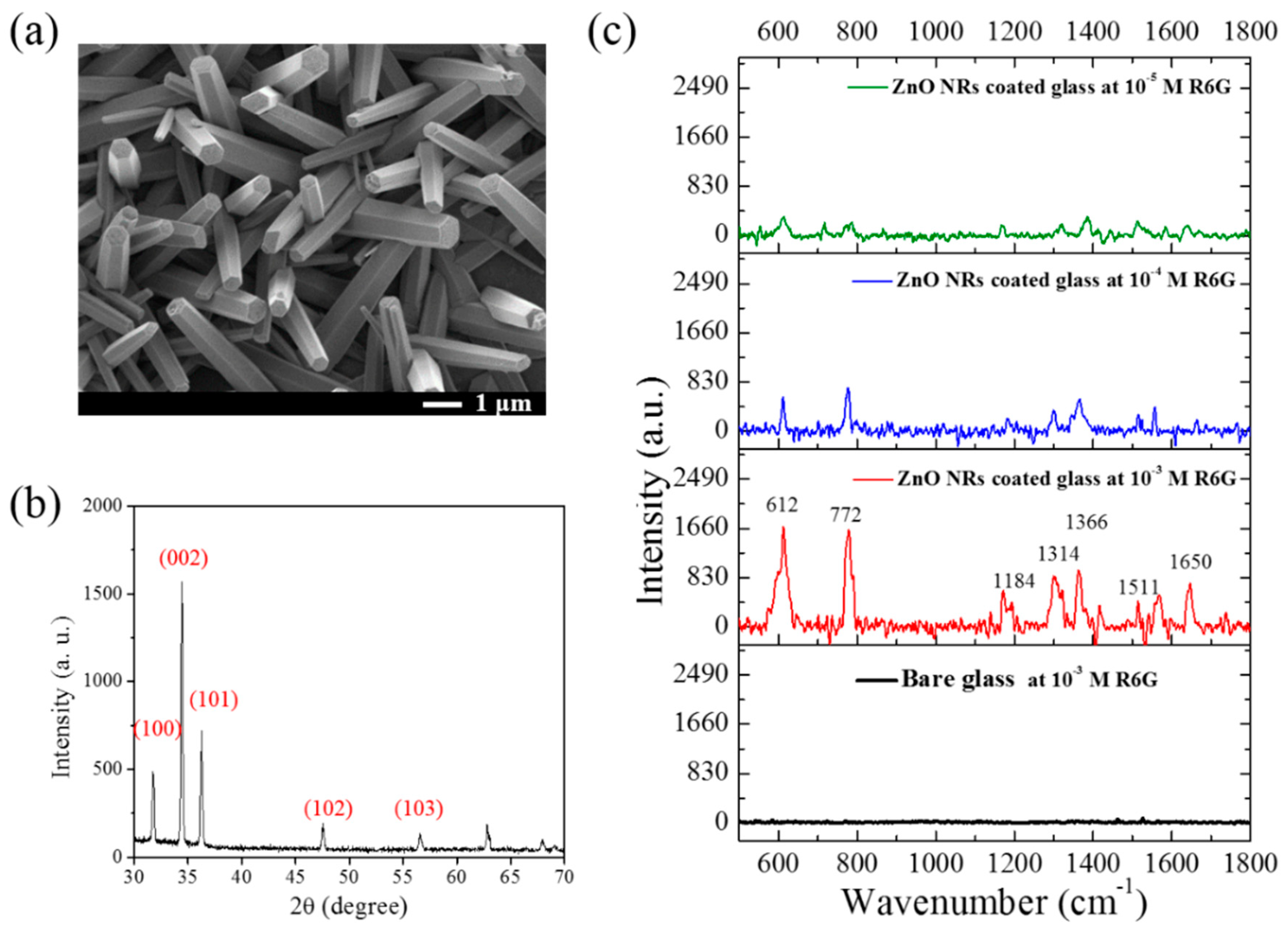
3.1. Surface Morphology, XRD and SERS Characteristic of ZnO NRs

The main advantage of growing ZnO NRs through dip coating and decorating AuNP through PLIP is that unlike complex sputtering deposition in high vacuum, the two-step process is a simple technique that allows precise control over the growth of ZnO seed layers. However, the ZnO seed layer may have a random coplanar orientation and a c-axis (002) perpendicular to the substrate, resulting in an incomplete c-axis orientation after chemical bath immersion [26]. Figure 2a illustrates the SEM images of the surface morphology of ZnO NRs, which reveals the hexagonal morphology of ZnO NRs with a diameter and length of approximately 300 nm and 4 μm, respectively and random orientation. During the growth of ZnO NRs, nucleation first occurs near the grain boundaries between two adjacent particles in the ZnO seed layer [27]. Not all nanowire arrays are c-axis orientated because of the polycrystalline nature of the seed layers [27,28]. Figure 2b depicts the XRD pattern of ZnO NRs, indicating a well-defined crystalline vertical c-axis (002), horizontal polar-terminated (001) and horizontal nonpolar low-symmetry (101) faces. The sharp XRD peaks prove the growth of the ZnO wurtzite structure [29]. Figure 2c depicts the Raman spectra of the R6G solution at various concentrations detected using ZnO NRs as the SERS substrate. Bare glass was also used as the substrate for the control experiment, which exhibited no Raman signal for 10−3 M R6G. Strong Raman signals were observed at 612, 772, 1184, 1314, 1366, 1511 and 1650 cm−1 on the ZnO NR SERS substrate for 10−3 M R6G, which were attributed to xanthene ring bending and deformations, C–H bond bending, N–H bond bending and CH2 waggling [22]. However, when the concentration of R6G was reduced to 10−5 M, the Raman signal was considerably weak.

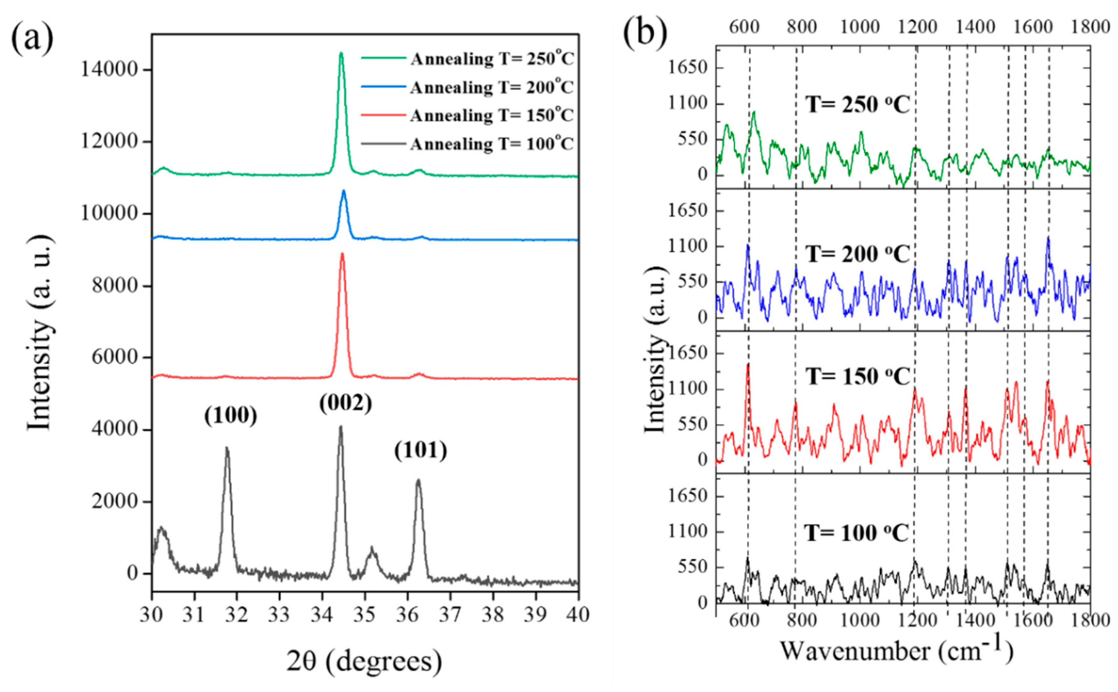
3.2. XRD, SERS and Surface Morphology of Annealed ZnO NRs

The quality of seed layers affects the preferred orientation of ZnO NRs. Previous studies have proved that surface morphology plays a critical role in the semiconducting nanostructure of the SERS substrate [4]. Therefore, we annealed seed layers at various temperatures to achieve superior ZnO NRs SERS substrates. Figure 3a illustrates the XRD patterns of ZnO NRs fabricated with annealed seed layers at various annealing temperatures. The polar-terminated (100) and nonpolar low-symmetry (101) faces disappeared in the ZnO NRs fabricated using seed layers annealed at temperatures higher than 150 °C. Figure 3b depicts the corresponding Raman signal for 10−3 M R6G, which indicated the enhanced Raman sensitivity of ZnO NRs grown using annealed seed layers. Figure S1 shows the SERS behaviors of ZnO NRs grown using annealed seed layers at the R6G concentration of 10−4 M and 10−5 M. Notably, the sample fabricated using ZnO seed layers annealed at 150 °C exhibited the highest sensitivity for the SERS signal. High annealing temperature was favorable for the growth of the c-axis (002) orientation and contributed to the increased SERS signal; however, the SERS signal decreased when the annealing temperature was higher than 150 °C. Figure 4 depicts the surface morphology of ZnO NRs fabricated using different seed layers annealed at various temperatures. The sample annealed at 100 °C exhibited a larger diameter (500 nm) of ZnO NRs than that of the unannealed sample (Figure 2a). However, the diameter of ZnO NRs decreased to 100 nm at the annealing temperature of 150 °C when using as-prepared seed layers. The diameter of ZnO NRs slightly increased at the annealing temperature of 250 °C. Compared with the corresponding SERS results in Figure 3b, applying the annealing technique when preparing seed layers decreased the diameter of ZnO NRs and further increased the SERS signal because of the increase in the surface-to-volume ratio of the SERS substrate. However, when the annealing temperature was higher than 150 °C, the diameter of ZnO NRs slightly increased, which was not favorable for the Raman signal enhancement of the ZnO NR SERS substrate.

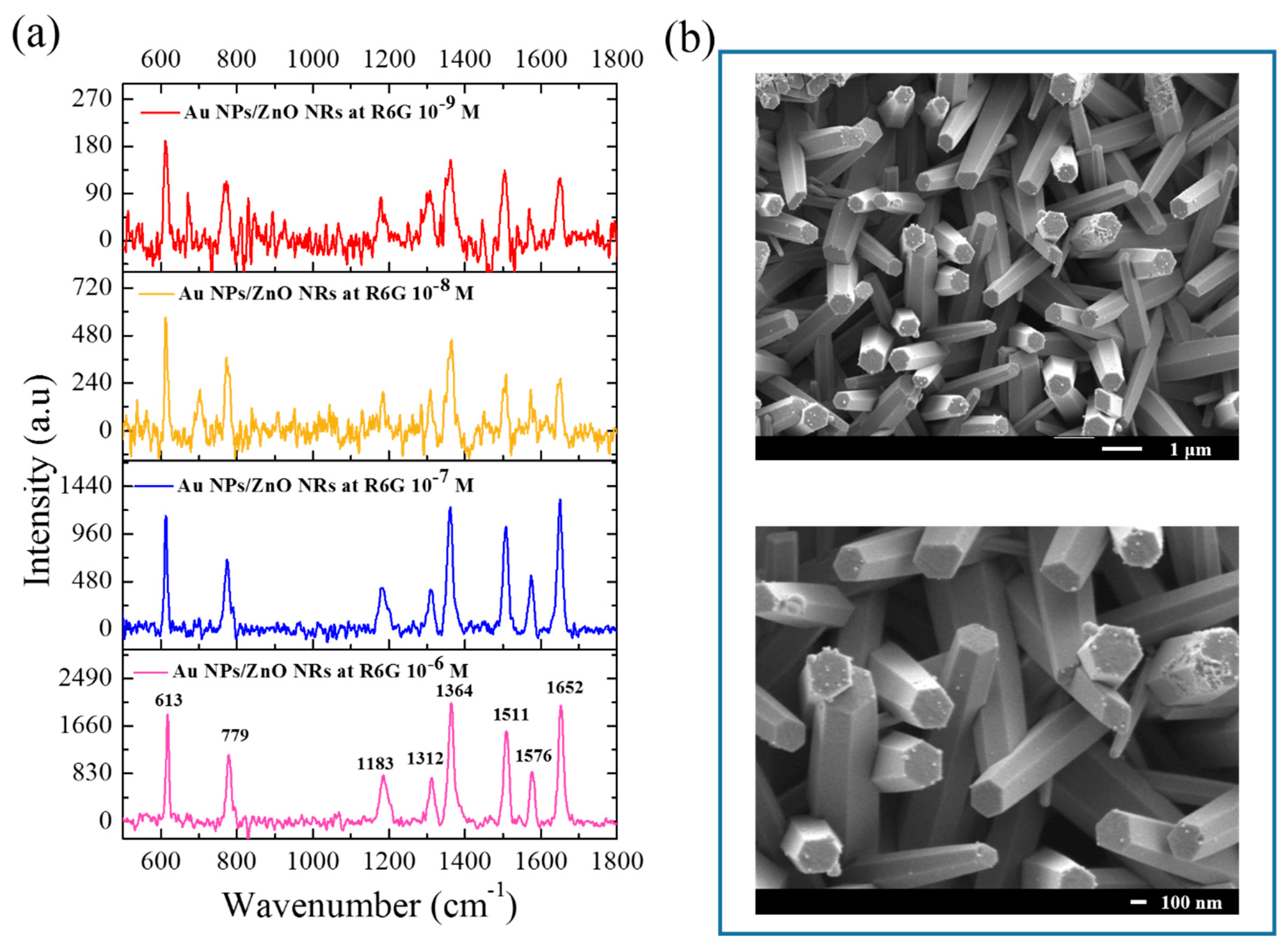
3.3. SERS and Surface Morphology of AuNP-Decorated ZnO NRs

Studies have shown the enhanced Raman signal using Au- or Ag-decorated ZnO NRs, in which the 3D shape of Au or Ag offers a “hot spot” and enhances the Raman signal in the resonance and nonresonance mode [10,12,14,16]. The CT occurs in the interface between metal and ZnO, with positively charged metal and negatively charged ZnO [20,21]. The Raman signal of the analyte absorbed on the ZnO nanostructure with an increased surface-to-volume ratio was further enhanced because of additional absorption from the LSPR mode (resonance) and CT (nonresonance). Therefore, to investigate the ability of the SERS effect using metallic NPs, we decorated ZnO NRs with AuNPs through PLIP. Figure S2 depicts the Raman signal of R6G using Au-decorated ZnO NRs at concentrations ranging from 10−6 to 10−9 M. Comparing to the undecorated ZnO NR SERS substrate (Figure 3b, annealed T = 150 °C), AuNPs did not have any effect on the enhancement of Raman signal. Figure 5 illustrates the SEM images of Au-decorated ZnO NRs, which indicated the nonhomogeneous distribution of AuNPs. Moreover, AuNPs aggregated on the top and between ZnO NRs. Studies have proved that the surface morphology of decorated metallic NPs plays a critical role in enhancing the Raman signal [10,12,14,16]. Only the 3D and isolated metallic NPs enhanced SERS effectively and further increased the Raman signal of the analyte. The surface morphology of ZnO NRs directly affects the size and the shape of grown AuNPs. Therefore, we grew AuNPs on unannealed ZnO NRs using the same PLIP method. Figure 6a depicts the Raman signal of R6G using Au-decorated ZnO NRs as the SERS substrate, in which ZnO NRs were fabricated using unannealed seed layers. Notably, the Raman signal of R6G was enhanced by reducing the full-width of half maximum. Figure 6b illustrates the SEM images of Au-decorated ZnO NRs, which reveal that AuNPs were independently grown on the top and sidewall of ZnO NRs. The surface morphology of Au-decorated ZnO NRs fabricated using annealed (Figure 5) and unannealed seed layers was compared (Figure 6b), which revealed that the annealed seed layers enhanced the growth of the ZnO NRs with (002) c-axis orientation and improved the Raman signal because of higher surface-to-volume ratio and density of ZnO NRs. However, the c-axis orientation and high density of ZnO NRs were favorable to the growth of closely packed and aggregated AuNPs and inhibited the growth of independent AuNPs, which hinders the formation of “hot spots” for SERS [20]. By contrast, ZnO NRs grown using unannealed seed layers resulted in ZnO NRs with a large diameter and horizontal (100) and (101) orientations, which are ineffective SERS substrates because of the low density and surface-to-volume ratio. However, AuNPs could be grown homogeneously and independently on ZnO NRs, such that AuNPs offers effective “hot spots” for SERS enhancement. Previous studies have used complex and time-consuming methods to achieve 3D metallic NPs on the ZnO nanostructure for enhancing SERS signals [10,12,14,16]. Our method is a simple method of fabricating Au-decorated ZnO NR SERS substrates in a short time.

3.4. SERS and Surface Morphology of AuNP-Decorated ZnO NRs by Changing the PLIP Conditions

Finally, we evaluated the experimental conditions of fabricating AuNPs using the PLIP method, followed by the immersion process, to grow AuNPs on ZnO NRs. Figure 7a depicts the Raman spectra of R6G using AuNP-decorated ZnO NRs as the SERS substrate for AuNP fabricated for different laser irradiation times at a fixed immersion time of 30 min. The results indicate that a short laser irradiation time of 8 min is suitable for fabricating AuNP-decorated ZnO NR SERS substrate to support the LSPR mode and enhance the Raman signal. A longer laser irradiation time of 20 min had the best ability of the SERS effect with the highest Raman intensity for the same FWHM from the Raman peak. The sample fabricated with the laser irradiation time for 30 min was not favorable for the SERS effect, and the Raman signal decreased. Figure 7b illustrates the Raman signal of R6G using AuNP-decorated ZnO NRs as the SERS substrate for AuNPs fabricated at different immersion times at fixed laser irradiation time of 8 min. A suitable immersion time facilitates the growth of AuNPs, and an immersion time of 30 min was the most suitable. The SERS sample with a longer immersion time exhibited a decrease in the Raman signal. Figure 7c depicts the SEM images of AuNP-decorated ZnO NRs for AuNPs fabrication at an immersion time of 60 min. Nonhomogeneous and aggregated AuNPs growth on ZnO NRs could be the cause of the weak Raman signal. We tried to correlate the size, density and the degree of agglomeration of AuNPs, observed in the SEM images (Figure 6b and Figure 7c), with the SERS enhancement and found out the size of AuNPs has to be in ~50-nm-diameter, the density of AuNPs has to be less than 10 AuNPs per ZnO NR, and the AuNPs has to be isolated and independently grown on each ZnO NR without aggregation.

4. Conclusions

We developed AuNP-decorated ZnO NRs as SERS substrates, in which AuNPs were fabricated through a chemically reduced and solution-based PLIP method. This method is a simple process and was completed in 30 min. ZnO NR fabrication using annealed seed layers increased the SERS signal. Analysis of surface morphology indicates that the decrease in the ZnO NR diameter and increase in the surface-to-volume ratio increased the sensitivity of Raman signal for detecting 10−5 M R6G. The SERS signal could be further improved by using AuNP-decorated ZnO NRs grown using unannealed ZnO seed layers. The use of unannealed seed layers facilitated the growth of ZnO NRs with non-preferred c-axis orientations and promoted the growth of homogeneous and individual AuNPs, which function as an effective “hot spots” for the Raman signal. Further studies of the AuNP fabrication using the PLIP method indicate that a short laser irradiation time of eight minutes, followed by a suitable chemical immersion time of 15–30 min are optimum conditions. Our results present an alternative method of fabricating effective SERS substrates in a simple wet chemical process combined with the short-time PLIP method.

Supplementary Materials

The following are available online at https://www.mdpi.com/2076-3417/10/14/5015/s1.

Author Contributions

Conceptualization, L.V.T.H. and V.K.S.H.; methodology, L.T.T.T., N.T.Q.N., S.-Y.L. and Y.-Z.F.; formal analysis, C.-M.C.; resources, L.V.T.H. and V.K.S.H.; data curation, L.T.T.T. and N.T.Q.N.; writing—original draft preparation, C.-M.C.; writing—review and editing, C.-M.C. and V.K.S.H.; supervision, L.V.T.H. and V.K.S.H.; project administration, S.-Y.L. and Y.-Z.F. All authors have read and agreed to the published version of the manuscript.

Funding

This research was funded by the Taichung Veterans General Hospital/National Chi Nan University Joint Research Program, Grant Number TCVGH-NCNU-1097902 and the Ministry of Science and Technology, Taiwan and Grant Number MOST-107-2221-E-260-016-MY3.

Conflicts of Interest

The authors declare no conflict of interest.

References

  1. Sharma, B.; Frontiera, R.R.; Henry, A.-I.; Ringe, E.; Van Duyne, R.P. SERS: Materials, applications, and the future. Mater. Today 2012, 15, 16–25. [Google Scholar] [CrossRef]
  2. Fleischmann, M.; Hendra, P.; McQuillan, A. Raman spectra of pyridine adsorbed at a silver electrode. Chem. Phys. Lett. 1974, 26, 163–166. [Google Scholar] [CrossRef]
  3. Alessandri, I.; Lombardi, J.R. Enhanced Raman Scattering with Dielectrics. Chem. Rev. 2016, 116, 14921–14981. [Google Scholar] [CrossRef] [PubMed]
  4. Wang, Z.L. Zinc oxide nanostructures: Growth, properties and applications. J. Phys. Condens. Matter 2004, 16, R829–R858. [Google Scholar] [CrossRef]
  5. Wang, Y.; Ruan, W.; Zhang, J.; Yang, B.; Xu, W.; Zhao, B.; Lombardi, J.R. Direct observation of surface-Enhanced Raman scattering in ZnO nanocrystals. J. Raman Spectrosc. 2009, 40, 1072–1077. [Google Scholar] [CrossRef]
  6. Wang, X.; She, G.; Xu, H.; Mu, L.; Shi, W. The surface-Enhanced Raman scattering from ZnO nanorod arrays and its application for chemosensors. Sens. Actuators B Chem. 2014, 193, 745–751. [Google Scholar] [CrossRef]
  7. Wang, X.; Shi, W.; She, G.; Mu, L. Surface-Enhanced Raman Scattering (SERS) on transition metal and semiconductor nanostructures. Phys. Chem. 2012, 14, 5891–5901. [Google Scholar] [CrossRef]
  8. Sun, Z.; Wang, C.; Yang, J.; Zhao, B.; Lombardi, J.R. Nanoparticle Metal−Semiconductor Charge Transfer in ZnO/PATP/Ag Assemblies by Surface-Enhanced Raman Spectroscopy. J. Phys. Chem. C 2008, 112, 6093–6098. [Google Scholar] [CrossRef]
  9. Cheng, C.; Yan, B.; Wong, S.M.; Li, X.; Zhou, W.; Yu, T.; Shen, Z.; Yu, H.; Fan, H.J. Fabrication and SERS Performance of Silver-Nanoparticle-Decorated Si/ZnO Nanotrees in Ordered Arrays. ACS Appl. Mater. Interfaces 2010, 2, 1824–1828. [Google Scholar] [CrossRef]
  10. Tang, H.; Meng, G.; Huang, Q.; Zhang, Z.; Huang, Z.; Zhu, C. Arrays of Cone-Shaped ZnO Nanorods Decorated with Ag Nanoparticles as 3D Surface-Enhanced Raman Scattering Substrates for Rapid Detection of Trace Polychlorinated Biphenyls. Adv. Funct. Mater. 2011, 22, 218–224. [Google Scholar] [CrossRef]
  11. Liu, K.; Li, D.; Li, R.; Wang, Q.; Pan, S.; Peng, W.; Chen, M. Silver-Decorated ZnO hexagonal nanoplate arrays as SERS-Active substrates: An experimental and simulation study. J. Mater. Res. 2013, 28, 3374–3383. [Google Scholar] [CrossRef]
  12. Xie, Y.; Yang, S.; Mao, Z.; Li, P.; Zhao, C.; Cohick, Z.; Huang, P.-H.; Huang, T.J. In Situ Fabrication of 3D Ag@ZnO Nanostructures for Microfluidic Surface-Enhanced Raman Scattering Systems. ACS Nano 2014, 8, 12175–12184. [Google Scholar] [CrossRef] [PubMed]
  13. Kandjani, A.E.; Mohammadtaheri, M.; Thakkar, A.; Bhargava, S.K.; Bansal, V. Zinc oxide/silver nanoarrays as reusable SERS substrates with controllable ‘Hot-Spots’ for highly reproducible molecular sensing. J. Colloid Interface Sci. 2014, 436, 251–257. [Google Scholar] [CrossRef]
  14. Tao, Q.; Li, S.; Ma, C.; Liu, K.; Zhang, Q.-Y. A highly sensitive and recyclable SERS substrate based on Ag-nanoparticle-Decorated ZnO nanoflowers in ordered arrays. Dalton Trans. 2015, 44, 3447–3453. [Google Scholar] [CrossRef] [PubMed]
  15. Huang, C.; Xu, C.; Lu, J.; Li, Z.; Xu, C. 3D Ag/ZnO hybrids for sensitive surface-Enhanced Raman scattering detection. Appl. Surf. Sci. 2016, 365, 291–295. [Google Scholar] [CrossRef]
  16. Tang, F.; Zhang, M.; Li, Z.; Du, Z.; Chen, B.; He, X.; Zhao, S. Hexagonally arranged arrays of urchin-Like Ag-Nanoparticle decorated ZnO-Nanorods grafted on PAN-Nanopillars as surface-Enhanced Raman scattering substrates. CrystEngComm. 2018, 20, 3550–3558. [Google Scholar] [CrossRef]
  17. Lin, R.; Hu, L.; Wang, J.; Zhang, W.; Ruan, S.; Zeng, Y.-J. Raman scattering enhancement of a single ZnO nanorod decorated with Ag nanoparticles: Synergies of defects and plasmons. Opt. Lett. 2018, 43, 2244–2247. [Google Scholar] [CrossRef]
  18. Lei, S.; Tao, C.; Li, J.; Zhao, X.; Wang, W. Visible light-induced charge transfer to improve sensitive surface-Enhanced Raman scattering of ZnO/Ag nanorod arrays. Appl. Surf. Sci. 2018, 452, 148–154. [Google Scholar] [CrossRef]
  19. Sedira, S.; Mounir, S. Surface enhanced Raman scattering (SERS) investigation and sensitive detection of zinc oxide nanorods (ZnO Nrds) deposited on silver nanoparticles (Ag NPs) substrate. Mater. Lett. 2019, 254, 112–115. [Google Scholar]
  20. Mishra, Y.K.; Mohapatra, S.; Singhal, R.; Avasthi, D.K.; Agarwal, D.C.; Ogale, S.B. Au–ZnO: A tunable localized surface plasmonic nanocomposite. Appl. Phys. Lett. 2008, 92, 043107. [Google Scholar] [CrossRef]
  21. Sakano, T.; Tanaka, Y.; Nishimura, R.; Nedyalkov, N.N.; Atanasov, P.A.; Saiki, T.; Obara, M. Surface enhanced Raman scattering properties using Au-Coated ZnO nanorods grown by two-Step, off-Axis pulsed laser deposition. J. Phys. D Appl. Phys. 2008, 41, 235304. [Google Scholar] [CrossRef]
  22. Chen, L.; Luo, L.; Chen, Z.; Zhang, M.; Zapien, J.A.; Lee, C.; Lee, S.T. ZnO/Au Composite Nanoarrays As Substrates for Surface-Enhanced Raman Scattering Detection. J. Phys. Chem. C 2009, 114, 93–100. [Google Scholar] [CrossRef]
  23. Sinha, G.; Depero, L.E.; Alessandri, I. Recyclable SERS Substrates Based on Au-Coated ZnO Nanorods. ACS Appl. Mater. Interfaces 2011, 3, 2557–2563. [Google Scholar] [CrossRef] [PubMed]
  24. Graniel, O.; Iatsunskyi, I.; Coy, E.; Humbert, C.; Barbillon, G.; Michel, T.; Maurin, D.; Balme, S.; Miele, P.; Bechelany, M. Au-Covered hollow urchin-Like ZnO nanostructures for surface-Enhanced Raman scattering sensing. J. Mater. Chem. C 2019, 7, 15066–15073. [Google Scholar] [CrossRef]
  25. Jue, M.; Lee, S.; Paulson, B.; Namgoong, J.-M.; Yu, H.Y.; Kim, G.; Jeon, S.; Shin, D.-M.; Choo, M.-S.; Joo, J.; et al. Optimization of ZnO Nanorod-Based Surface Enhanced Raman Scattering Substrates for Bio-Applications. Nanomaterials 2019, 9, 447. [Google Scholar] [CrossRef] [Green Version]
  26. Ohyama, M.; Kouzuka, H.; Yoko, T. Sol-Gel preparation of ZnO films with extremely preferred orientation along (002) plane from zinc acetate solution. Thin Solid Film. 1997, 306, 78–85. [Google Scholar] [CrossRef]
  27. Vayssieres, L. Growth of Arrayed Nanorods and Nanowires of ZnO from Aqueous Solutions. Adv. Mater. 2003, 15, 464–466. [Google Scholar] [CrossRef]
  28. Yu, H.; Zhang, Z.; Han, M.; Hao, X.-T.; Zhu, F. A General Low-Temperature Route for Large-Scale Fabrication of Highly Oriented ZnO Nanorod/Nanotube Arrays. J. Am. Chem. Soc. 2005, 127, 2378–2379. [Google Scholar] [CrossRef]
  29. Yamabi, S.; Imai, H. Growth conditions for wurtzite zinc oxide films in aqueous solutions. J. Mater. Chem. 2002, 12, 3773–3778. [Google Scholar] [CrossRef]
Figure 1. Schematic of fabricating surface-enhanced Raman scattering (SERS) substrate using zinc oxide (ZnO) nanorods (NRs) decorated with Au nanoparticles (AuNPs) synthesized through pulsed-laser-induced photolysis (PLIP).
Applsci 10 05015 g001
Figure 2. (a) SEM image of ZnO NRs fabricated using the sol–gel method on a glass substrate; (b) XRD patterns of ZnO NRs fabricated by the unannealed seed layer, indicating both vertical (002) and horizontal (100) and (101) growth direction; (c) Raman signal of rhodamine 6G (R6G) using bare glass and ZnO NR-coated glass as surface-enhanced Raman scattering (SERS) substrates.
Applsci 10 05015 g002
Figure 3. (a) XRD patterns of annealed ZnO NRs indicating the disappearance of horizontal (100) and (101) growth direction with the increase in the annealing temperature applied on the growth of seed layers; (b) Raman signal of R6G (10−3 M) using ZnO NR-coated glass as the SERS substrate, in which ZnO NRs were fabricated using seed layers annealed at different temperatures.
Applsci 10 05015 g003
Figure 4. SEM images of ZnO NRs fabricated using seed layers annealed at (a) 100 °C, (b) 150 °C, (c) 200 °C and (d) 250 °C.
Applsci 10 05015 g004
Figure 5. SEM images of Au-decorated ZnO NRs of different magnification.
Applsci 10 05015 g005
Figure 6. (a) Raman signal of R6G at different concentrations using Au-decorated ZnO NRs as the SERS substrate where the ZnO NRs was fabricated using the unannealed seed layer; (b) corresponding SEM images of Au-decorated ZnO NRs of different magnification.
Applsci 10 05015 g006
Figure 7. Raman signal of R6G (10−6 M) at various concentrations using Au-decorated ZnO NRs as the SERS substrate for AuNP fabrication for (a) different laser irradiation times at a fixed immersion time of 15 min and (b) different immersion time at a fixed laser irradiation time of 8 min during PLIP; (c) corresponding SEM images of Au-decorated ZnO NRs fabricated using an immersion time of 60 min.
Applsci 10 05015 g007

