1. Introduction
Digital coherent optical transmission is currently the mainstream scheme used for medium-to-long-distance optical communication, where it is optimal from the standpoint of spectral efficiency as it allows for the encoding of information in both quadrants and polarization of the electric field [
1,
2]. However, the cost of a coherent receiver, which requires highly customized hardware and complex compensation algorithms, is unacceptably high for short-range links, such as intra-datacenter interconnections [
3,
4,
5].
In recent years, the requirement for alternatives to digital coherent transmission in short-reach applications has spawned a series of studies on direct detection (DD) systems due to their low cost, high power efficiency, and easy implementation [
6,
7,
8,
9,
10,
11,
12,
13,
14,
15,
16,
17,
18,
19]. Some schemes have been proposed in the published literature. The earliest is the on–off keying (OOK) scheme for low-speed communications [
6], which is also the simplest but has high bandwidth and fiber dispersion matching requirements. To improve the spectral efficiency, high-order modulation formats are adopted. The most common is the pulse-amplitude modulation (PAM) scheme, which encodes information at multiple amplitude levels, such as PAM-4 [
7] and PAM-8 [
8]. However, the reception sensitivity will be significantly reduced as the level increases. Two other popular approaches are carrier-less amplitude and phase (CAP) modulation and discrete multi-tone (DMT) modulation [
9,
10,
11]. CAP is relatively simple to implement in real time, while DMT offers lower computational complexity. However, both of them have a low tolerance for linear propagation effects. To this end, a self-coherent heterodyne scheme was proposed by Lowery and Armstrong [
12,
13], which requires transmitting a frequency offset local oscillator (LO), together with the signal, thereby allowing for a complete reconstruction of the complex-valued field. More recently, some other schemes that are capable of full-field reconstruction, including Stokes vector direct detection (SV-DD) [
14,
15], single-sideband modulation/direct-detection (SSB-DD) [
16,
17], and Kramers–Kronig (KK) receivers [
18,
19], have been proposed. It is noteworthy that these schemes all require an auxiliary signal from the transmitter to enable full-field reconstruction at the receiver.
In this study, a dual-polarization quadrature phase-shift keying modulation/direct detection (DP-QPSK-DD) scheme for short-range optical communications was investigated. Compared with traditional binary modulation formats (OOK, BPSK (Binary Phase Shift Keying), etc.), DP-QPSK is modulated in multiple dimensions of polarization, phase, and amplitude at the same time, with greater degrees of freedom and lower complexity in each dimension, which gives it the advantage of a narrower spectral width, higher spectral efficiency, and higher tolerance to various fiber-based transmission impairments [
20]. Hence, DP-QPSK is one of the mainstream modulation formats in the current 100 Gbps optical communication systems and is one of the solutions used for 400 Gbps optical transmission [
21,
22]. The DP-DQPSK-DD scheme is implemented based on a delay-line interferometer (DLI), which has simple and low-cost hardware implementation and is an ideal alternative to digital coherent transmission for short-range, non-cooperative communication. We propose an algorithm for recovering the raw data from the transmitting end. Based on this, we also studied measures used to improve the performance of the DP-QPSK reception and it was found that appropriately decreasing the free spectral range (FSR) of the DLI could increase the tolerance to transmission impairments to a certain extent.
The remainder of this paper is organized as follows.
Section 2 briefly introduces the structure and basic principle of the DLI-based DP-QPSK-DD system. The data recovery algorithm is proposed in
Section 3. In
Section 4, the impact of FSR adjustment is analyzed theoretically. Simulations are conducted in
Section 5 to verify the feasibility of the algorithm and the effect of decreasing the FSR of the DLI. Finally, conclusions are given in
Section 6.
2. Structure and Basic Principle
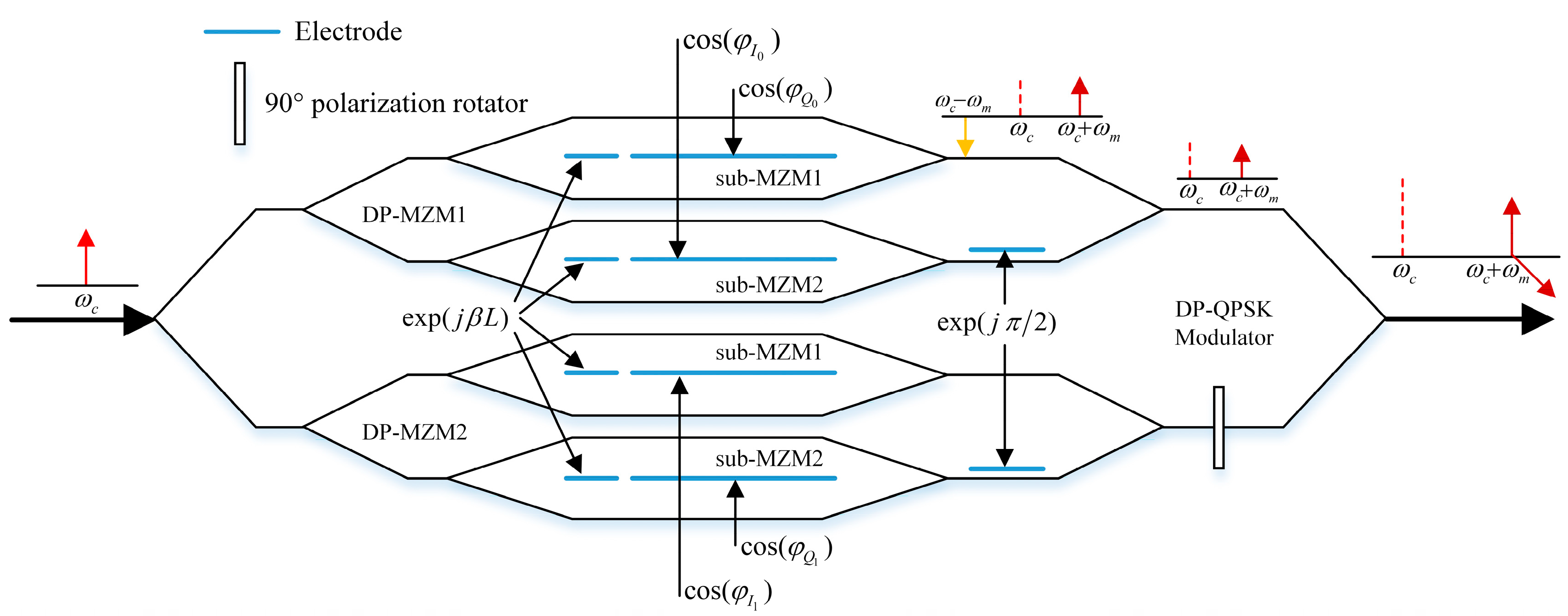
DP-QPSK is most commonly modulated at the transmitter through electro-optic modulators based on a Mach–Zehnder interferometer structure, which was first proposed by Zehnder in 1891 and improved by Mach in 1892 [
23,
24].
Figure 1 gives the detailed structure of the DP-QPSK modulator and shows how it works.
A linearly polarized continuous-wave (CW) lightwave emitted from a laser diode (LD) is injected into a DP-QPSK modulator [
25]. It was assumed that the optical signal at the input of the modulator was:
where
is the optical power,
is the optical frequency, and
is the initial phase.
A DP-QPSK modulator mainly consists of four Mach–Zehnder modulators (MZM) and a 90° polarization rotator. Every two MZMs are connected in parallel or in series to form a DP-MZM. The transfer equation of an MZM biased at the minimum transmission point is [
25,
26]:
where
is the input signal into the MZM,
is the modulation coefficient of the MZM,
is the length of the electrode,
is the half-wave voltage of the MZM, and
and
are the drive voltages of the MZM. In
Figure 1,
, which is the baseband signal to be modulated. Each DP-MZM is biased on one arm to introduce a 90° phase shift. Hence, the output of the DP-MZM is:
where
is the modulated phase. Then, one of the DP-MZM output signals is applied to a polarizer and the two DP-MZM outputs give the two orthogonal polarization states. The output DP-QPSK signal can be written as follows:
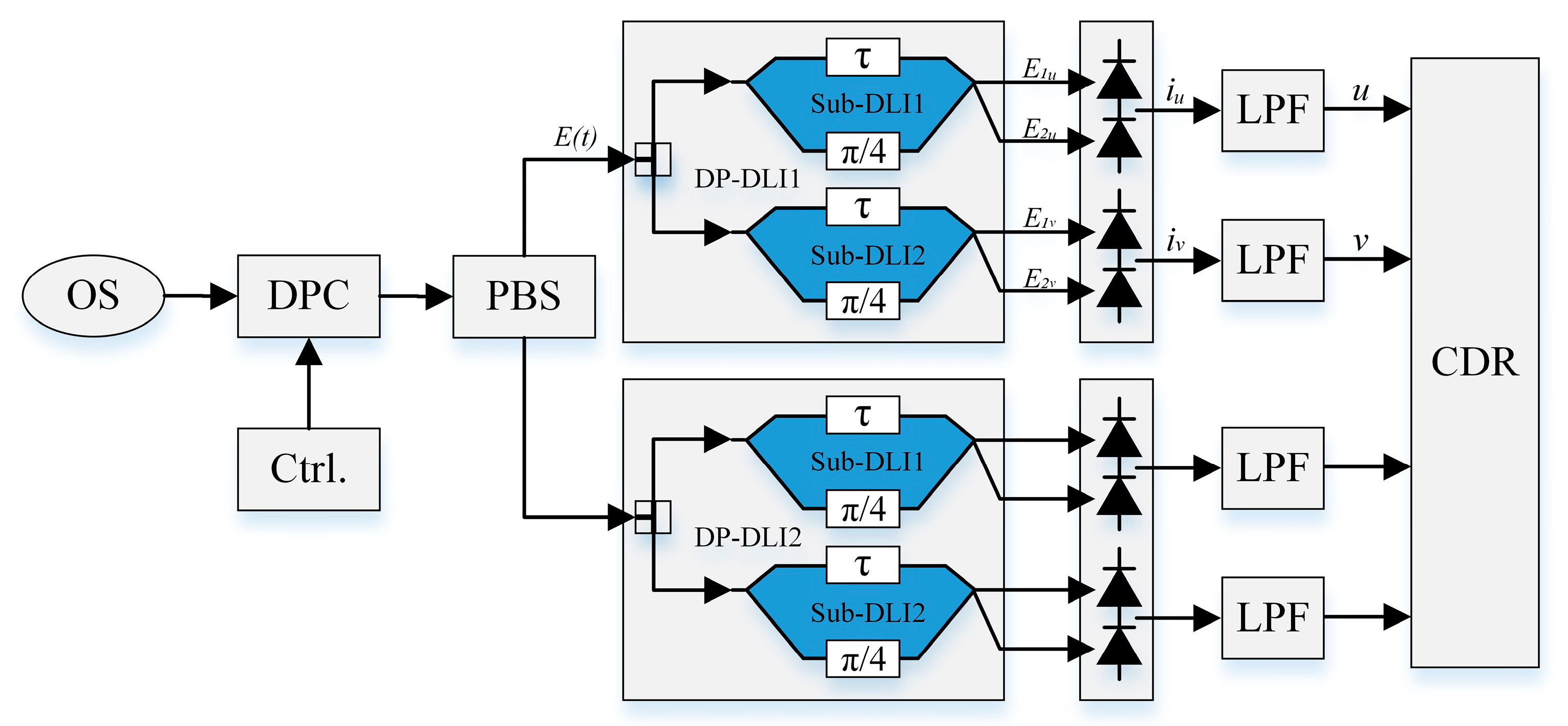
The optical signal from the transmitter is transmitted through a fiber-optic link and reaches the receiver for demodulation. The structure of a DLI-based DP-QPSK receiver is schematically shown in
Figure 2. A DP-QPSK demodulator is mainly composed of two DP-DLIs and four pairs of balanced photodiodes. Each DP-DLI consists of two Mach–Zehnder DLIs and every DLI is traditionally tuned with an exact one-symbol-period differential delay on one arm and a +45° (−45°) phase shift on the other, which is the most efficient configuration in back-to-back systems [
27,
28].
The input optical signal is separated through a dynamic polarization alignment controller (DPC) and a polarization beam splitter (PBS) into two signals with mutually orthogonal polarization states, realizing polarization demultiplexing. The separated single-polarized signals are then injected into a DP-DLI each, which converts the phase-difference information into intensity information in the optical domain. Finally, signals containing the intensity information are directly detected through balanced photodiodes and high-frequency noise is eliminated after filtering. The raw data is recovered using subsequent devices. It is noteworthy that the LPF used here is a manifestation of the low-pass characteristics of the hardware, which result from the limitations of the hardware itself. For example, limitations in the frequency response of the photodiodes prevent high-frequency components from passing through it.
Assuming that the responsibilities of photodiodes are the same, all being equal to
, the differential delay in the time domain is
, and the signal at the input of DP-DLI is
, where
A is the amplitude,
is the carrier phase, and
is the signal phase. The optical signal at the output of the DP-DLI can be expressed as:
According to the square-law characteristic of photodiodes, the converted photocurrent is (taking
as an example here):
After the balanced photodetectors, the two electrical signals can be written as:
where
is the phase difference between adjacent symbols.
3. The Data Recovery Algorithm
In this section, the data recovery algorithm for DLI-based DP-QPSK reception is presented. Considering the limitations of the algorithm, assumptions were made first. Signals are usually transmitted in the form of frames in the channel and frame synchronization should be done first at the receiver before subsequent processing. There are two main types of frame synchronization techniques: one is data-aided frame synchronization, in which a predetermined synchronization word is periodically inserted in a frame, and the other is code-property-aided frame synchronization, in which the data is encoded with an error correction encoder. For the former, synchronization is attained through recognizing the synchronization word, while for the latter, synchronization is attained through exploiting the properties of the code. In this study, we only considered the data-aided frame synchronization technique. Hence, we assumed that a predetermined synchronization code was periodically inserted in the raw data before modulation for the receiver to obtain data synchronization. Moreover, the payload in the raw data was random. Based on these two assumptions, the data recovery algorithm was proposed as follows.
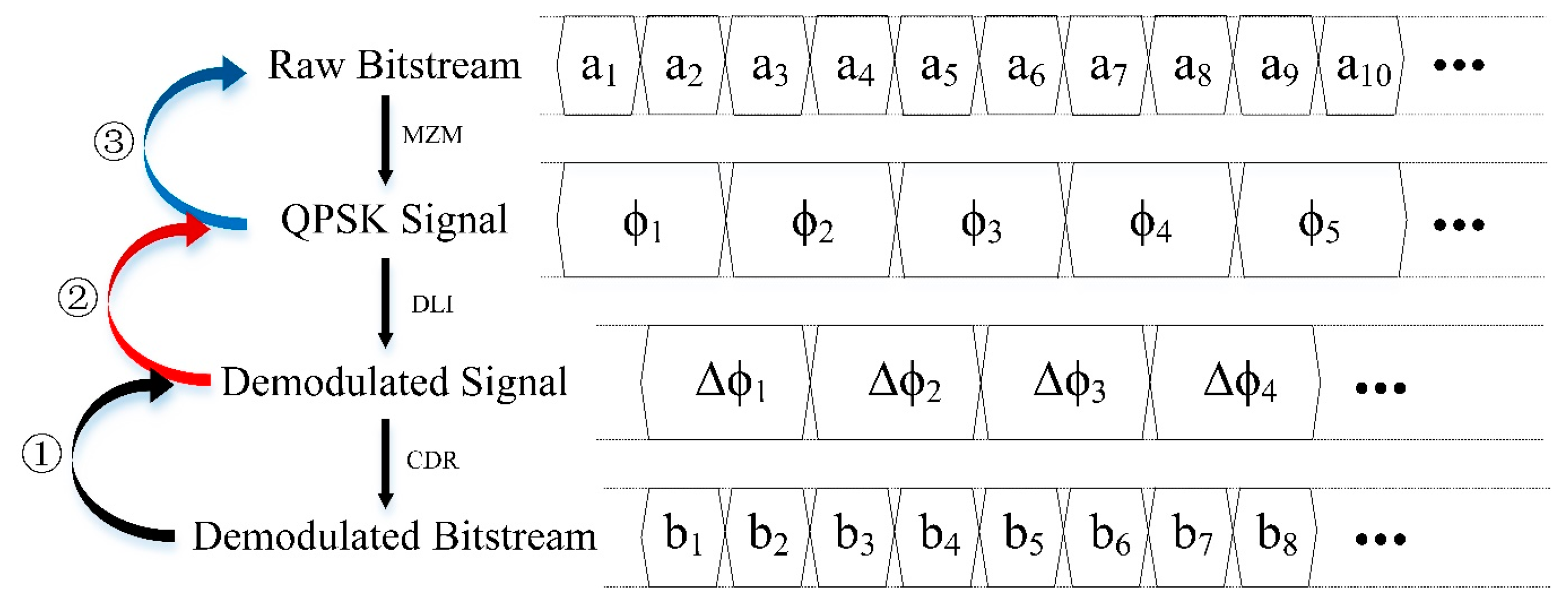
DP-QPSK modulation lacks the process of differential precoding, while the output of a DLI-based demodulator is the information of phase differences between adjacent symbols. Hence, further data processing is required to recover the raw data.
Figure 3 shows the conversion of data flow in a single polarization state in the DLI-based DP-QPSK transmission system. The raw bitstream is modulated to a QPSK signal by the MZM at the transmitting end and the QPSK signal is processed through a DLI and CDR into a demodulated bitstream at the receiving end. It is a reverse engineering problem to recover the raw data from the demodulated bitstream and a three-step inverse mapping is required.
Inverse mapping 1 from the demodulated bitstream to the demodulated signal: From Equation (6), we can find the correspondence between them, which is shown in
Table 1. Therefore, the inverse mapping can be completed by just referring to
Table 1.
Inverse mapping 2 from the demodulated signal to the QPSK signal: The demodulated signal is the phase difference information and the QPSK signal is the phase information, which means the initial phase
is required to complete the inverse mapping. QPSK characterizes different dual-bit symbols with four different phases in two modes, namely, mode A and mode B, corresponding to the parallel modulation and series modulation, respectively. The correspondence is shown in
Table 2. Therefore, there are eight possible values for
and the eight cases need to be verified one by one in the next step.
Inverse mapping 3 from the QPSK signal to the raw bitstream: The inverse mapping of this step can be completed by referring to
Table 2, while for the eight cases caused due to the unknown initial phase, we need to search every bitstream for the frame synchronization code, which only appears in the raw data.
Based on the three-step inverse mapping above, the data recovery algorithm can be summarized as follows.
| Algorithm 1 Recover the raw data from the demodulated bitstream |
 |
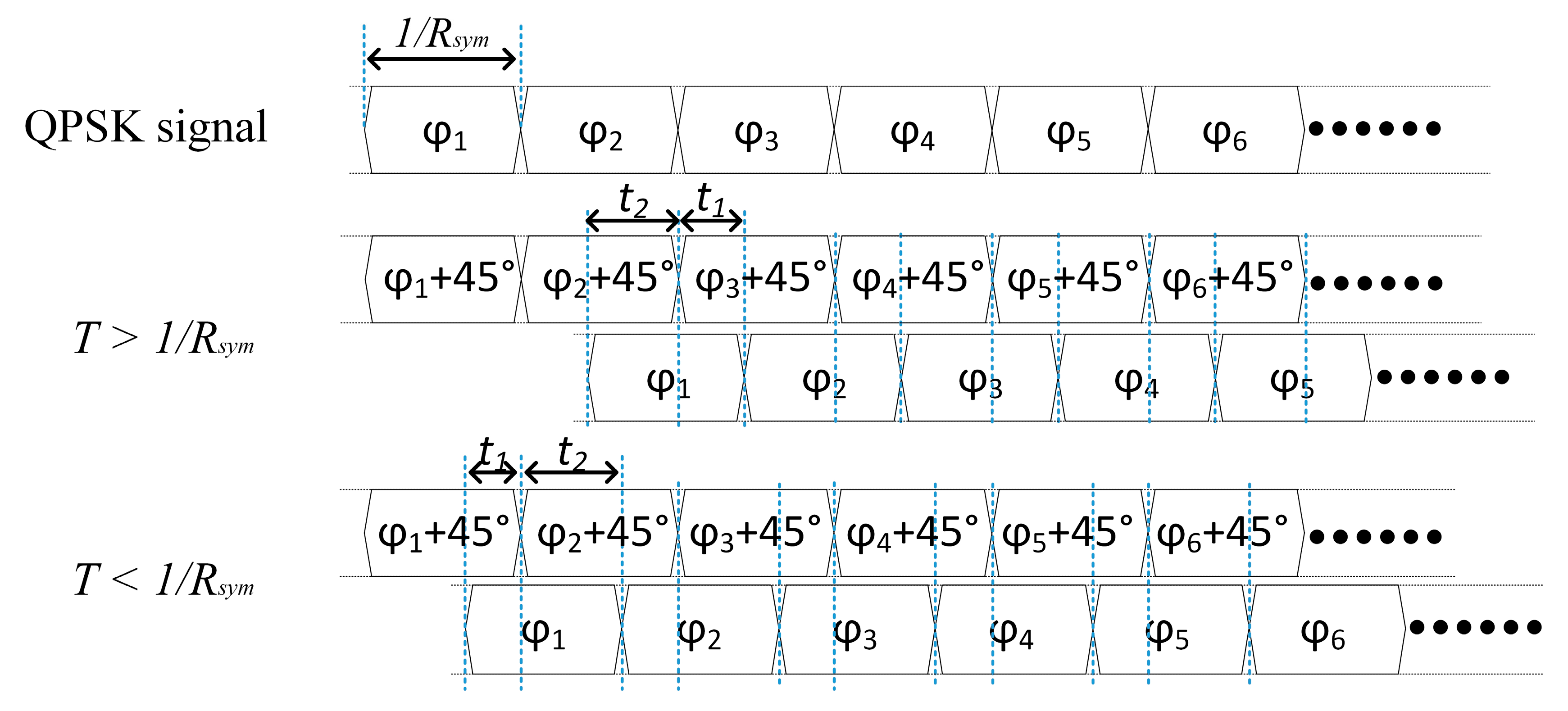
4. FSR Optimization
Traditionally, DLI is configured with an exactly one-symbol-period differential delay on one arm and a 45° (−45°) phase shift on the other, which means the FSR of the DLI is equal to the transmission symbol rate. It has already been shown through simulations that decreasing the differential delay led to increased chromatic dispersion tolerances in DLI-based BPSK demodulation [
28,
29,
30]. This study first qualitatively analyzed the effect of FSR adjustment on DP-QPSK demodulation performance through a theoretical derivation. The two cases of FSR increasing and decreasing are shown in
Figure 4.
When decreasing the differential delay of the DLI to less than one symbol period, part of a symbol interferes with itself. The signals before the photodetectors can be expressed as:
The converted photocurrent is (taking
as an example here):
After the balanced photodetectors, the two electrical signals can be written as (the DC component is ignored here):
The situation of increasing the delay to greater than one symbol period is shown in
Figure 4. The signals before the photodetectors can be expressed as:
The converted photocurrent is (taking
as an example here):
After the balanced photodetectors, the two electrical signals can be written as (the DC component is ignored here):
It should be noted that the above formulas were derived without considering the noise. Since
and
obtained using Equations (7), (10), and (13) are subsequently compared to the set threshold for a 0–1 judgment, the impact of noise cannot be ignored.
Figure 5 gives a schematic diagram of the 0–1 judgment and the noise was introduced. It can be seen from
Figure 5 that the smaller
was, the greater the probability of misjudging will be in the presence of the noise.
Based on the formula derivations for the three situations, a qualitative analysis could be conducted. Since the possible set of values for the phase difference
was
, according to Equations (6) and (9), the photodetector output of case 1 was larger than that of the situation with an exactly one-symbol delay, which created a deterministic constructive interference for every symbol period. The deterministic constructive interference could suppress the inter-symbol crosstalk that resulted from transmission impairments to a certain extent. It can also be known from Equation (10) and
Figure 5 that the decrease of
will increase the error rate of the final judgment. Hence, decreasing the differential delay can both increase the tolerance of transmission impairments and increase the BER for receivers. As for case 2, it can be seen from Equations (12) and (13) that the photodetector output did not show any advantage over the situation with an exactly one-symbol delay due to the presence of
. Therefore, case 2 was not taken into consideration in the following simulation.
5. Simulations
Simulations were conducted for a 112 Gbps DP-QPSK signal with a laser at 193.1 THz, modulated on two orthogonal polarization states, and the two sub-MZMs with an extinction ratio of 60 dB in each DP-MZM were configured in parallel. The receiver consisted of a 70 GHz third-order Gaussian optical filter, two tunable DP-DLIs followed by four pairs of balanced photodetectors, and four 21 GHz fourth-order Bessel electrical filters. The simulations were carried out in Optisystem 15 from company Optiwave in Ottawa, Ontaria, Canada.
5.1. Data Recovery Algorithm
In the algorithm simulation experiment, a string of a pseudo-random binary sequence (PRBS) is generated first and is divided into a series of frames with 1024-bit lengths. A fixed sequence 0xf628 is inserted between every two frames as the frame synchronization code. The new sequence is then applied to DP-MZM as the raw signal for modulation.
In fact, the searching algorithm plays an important role in our data recovery algorithm. This study applied a frame parameter recognition algorithm based on self-correlation to search for the frame synchronization code, and the recognition accuracy rate is claimed to be very high when bit error rate (BER) is less than 0.02 [
31,
32]. In this algorithm, the frame length is searched first within a given range based on self-correlation and a peak-to-average ratio, and thresholds are set to obtain a credible frame length estimation value. Then, the synchronization code is recognized and thresholds are set to distinguish between 0 and 1. To simplify the simulation, we assumed that the frame length was known to the receiving end. If a clear correlation peak appears, which means a fixed frame synchronization code existed in the bitstream, the sequence is considered as the raw data. Otherwise, it is not.
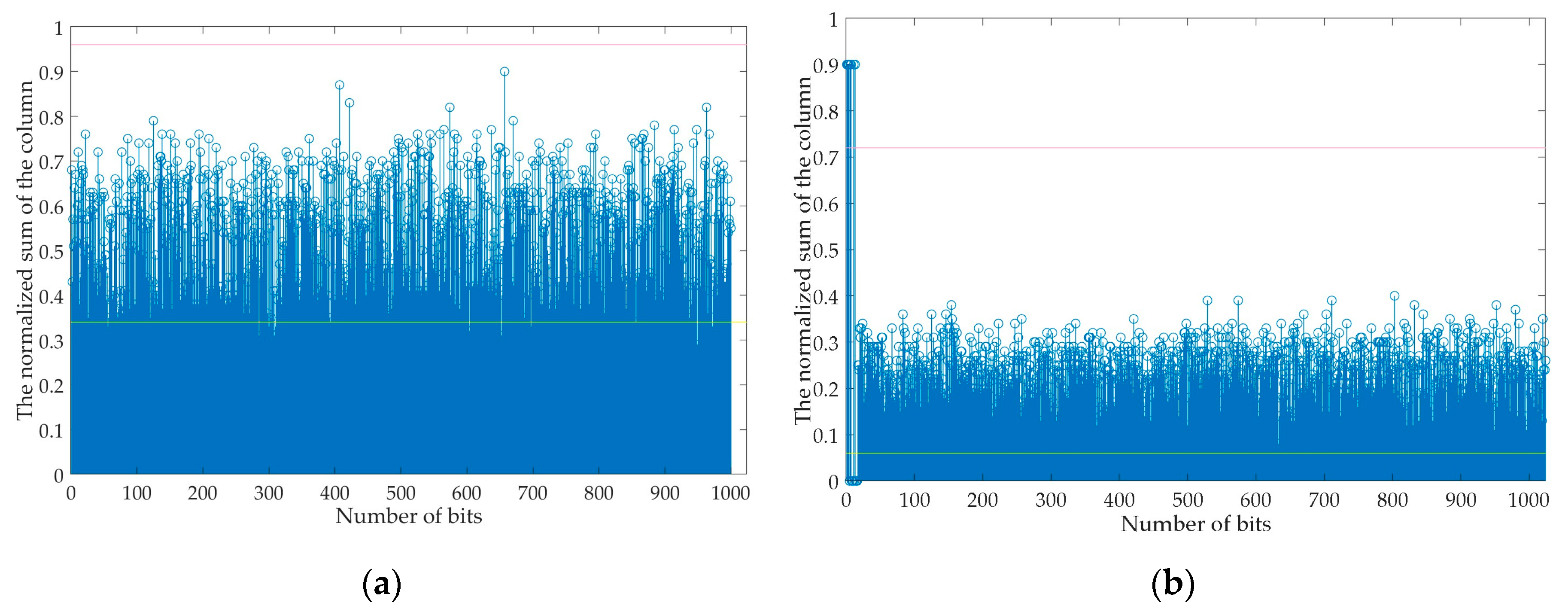
Figure 6 gives the frame synchronization code recognition result of one simulation. The upper and lower thresholds in
Figure 6a were set to determine the frame length, and the thresholds in
Figure 6b were set to recognize the synchronization code. The bitstream with a clear correlation peak appearing was highly consistent with the raw data. Given that bit errors existed during demodulation, we considered the bitstreams with a correlation peak as the raw data.
5.2. FSR Optimization
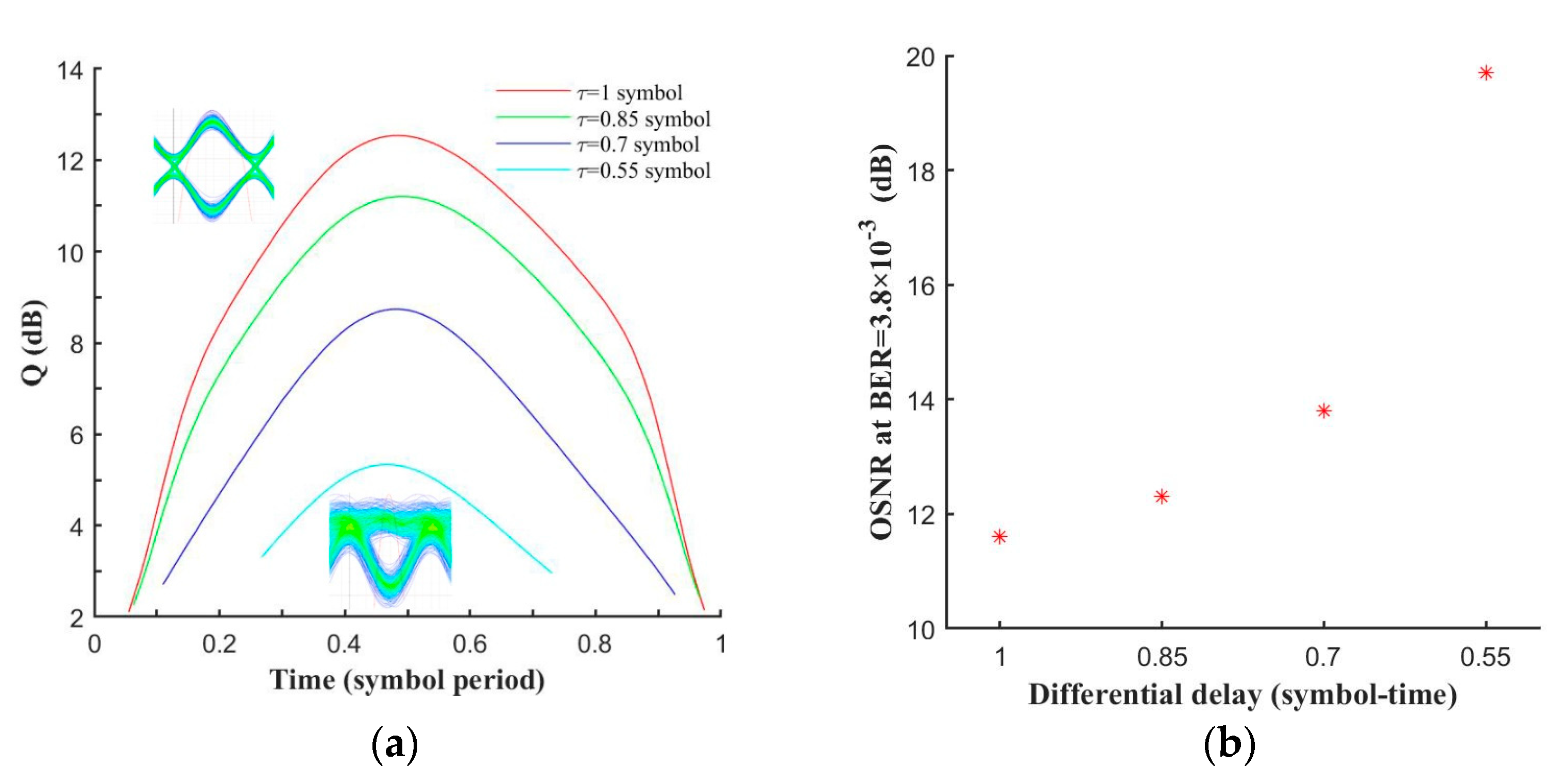
First, we compared the performances of the receivers with the DLI in different differential delays in a back-to-back configuration and the results are presented in
Figure 7.
The receiver’s BER versus the DLI differential delay under the same optical signal-to-noise ratio (OSNR) is shown in
Figure 7a and the given OSNR here is 15 dB. The Q parameter was calculated from BER using the formula
.
Figure 7b shows the OSNR required for receivers with different DLI delays at the FEC threshold of BER = 3.8 × 10
−3. The simulation results were consistent with the theoretical derivation above. Eye diagrams of a one-symbol-period delay and a 0.55-symbol-period delay are given in
Figure 7a and a serious eye closure was created when the differential delay of DLI was a 0.55-symbol period. From
Figure 7b, we can see that the OSNR penalty increased almost exponentially with the decrease of the differential delay.
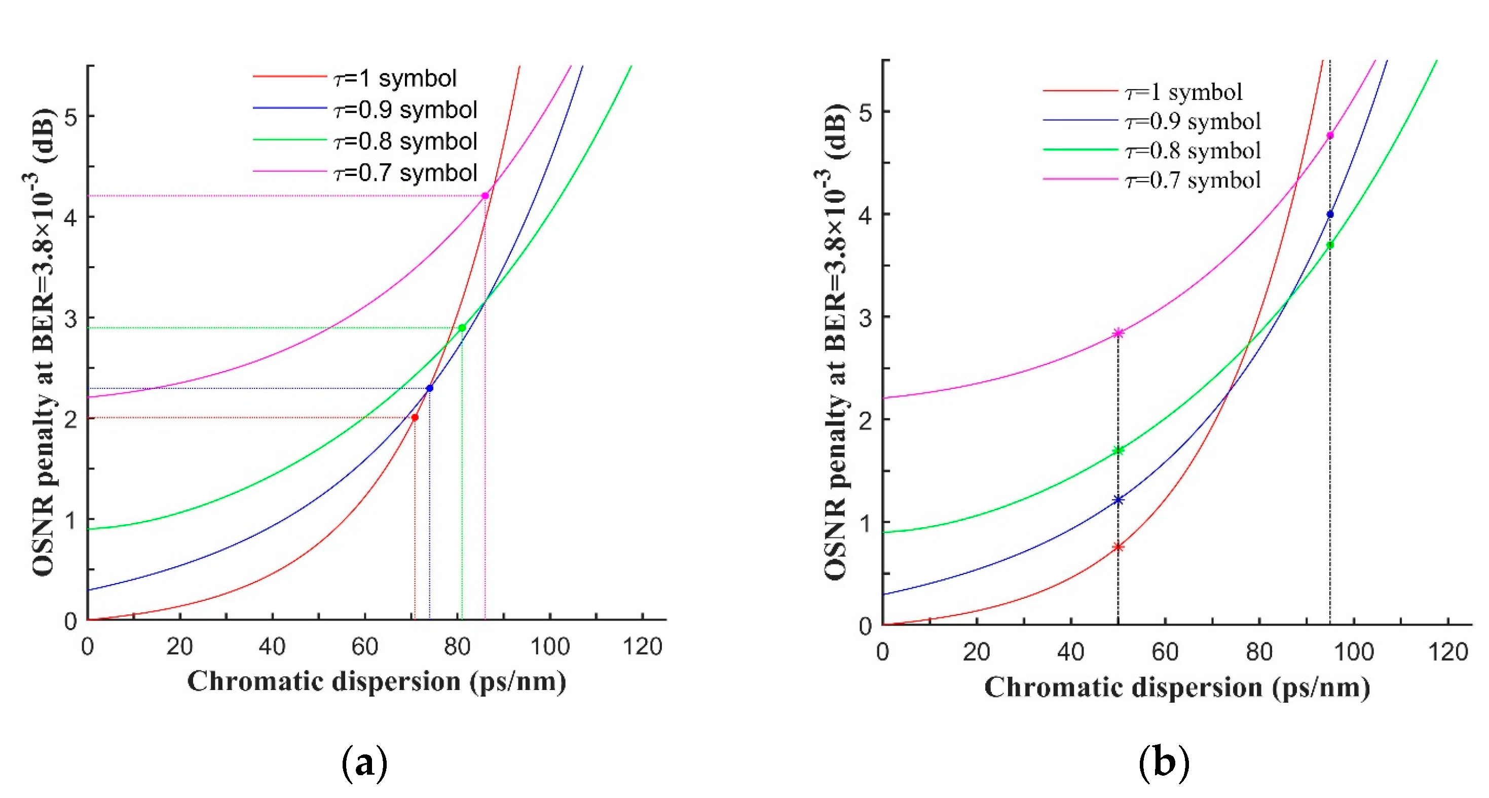
The chromatic dispersion tolerance of the receivers with different DLI delays were measured and the results are shown in
Figure 8.
In the simulations, the result of the back-to-back configuration with an exactly one-symbol-period delay was used as a zero point for the OSNR penalty. We recorded the OSNR penalty of different differential delays at BER = 3.8 × 10
−3 while gradually increasing the system’s chromatic dispersion. The intersections of the curves and the
y-axis in
Figure 8 reflect the OSNR penalty of simply decreasing the differential delay without introducing dispersion. We can see that the OSNR penalty for receivers with a 0.9-symbol-period delay, a 0.8-symbol-period delay, and a 0.7-symbol-period delay were 0.3 dB, 0.9 dB, and 2.2 dB, respectively.
In
Figure 8a, the points marked on the curves indicate the dispersion tolerance due to the 2 dB OSNR penalty of the receivers. The 2 dB chromatic dispersion tolerances were 70.8 ps/nm, 74 ps/nm, 81.2 ps/nm, and 84.5 ps/nm for receivers with a 1-symbol-period delay, a 0.9-symbol-period delay, a 0.8-symbol-period delay, and a 0.7-symbol-period delay, respectively. It can be seen that the 2 dB dispersion tolerance was increased by nearly 20% when the DLI differential delay was a 0.7-symbol period. The OSNR penalty required for receivers with different delays to maintain a BER of 3.8 × 10
−3 under the same system dispersion are compared in
Figure 8b. The results suggest that by considering the OSNR penalty introduced by only decreasing the differential delay, the optimal delay for a receiver with a system chromatic dispersion of 50 ps/nm was one symbol period, while the optimal delay was a 0.8-symbol period for a receiver with a dispersion of 95 ps/nm. It can be drawn from
Figure 8b that the optimal delay of the DLI was inversely proportional to the chromatic dispersion, which is consistent with the previously reported results on BPSK demodulation [
15].
6. Conclusions
In this study, the structure and basic principles of a DLI-based DP-QPSK transmission system were briefly introduced. A data recovery algorithm was proposed for a receiver based on DLI that could recover raw data due to the lack of a differential precoding process in the DP-QPSK modulation. Measures to improve the demodulation performance were further studied and it was shown through theoretical derivation that appropriately increasing the FSR of DLI could achieve the goal. The simulation results showed that the algorithm was effective for recovering the raw data in a DLI-based DP-QPSK receiver and the 2 dB dispersion tolerance was increased by nearly 20% when decreasing the delay to a 0.7-symbol period under the simulation configuration set in this study. Hence, the DLI-based receiving scheme for a DP-QPSK is an ideal solution for short-range, non-cooperative communication. It is noteworthy that the performance of the data recovery algorithm depends to a certain extent on the frame synchronization algorithm, which will need to be optimized in our future work.
Author Contributions
Conceptualization, H.Y. and Y.Y.; methodology, H.Y.; software, H.Y.; supervision, Z.H.; validation, Y.Y.; writing—original draft, H.Y.; writing—review and editing, H.Y. and Y.Y. All authors have read and agreed to the published version of the manuscript.
Funding
This research was supported by the National Natural Science Foundation of China (General Program), grant no. 51575517.
Conflicts of Interest
The authors declare no conflict of interest.
References
- Shieh, W.; Athaudage, C. Coherent optical orthogonal frequency division multiplexing. Electron. Lett. 2006, 42, 587–589. [Google Scholar] [CrossRef]
- Arnhem, M.; Karpov, E.; Cerf, N.J. Optimal estimation of parameters encoded in quantum coherent state quadratures. Appl. Sci. 2019, 9, 4264. [Google Scholar] [CrossRef]
- Zhao, J.; Liu, Y.; Xu, T. Advanced DSP for coherent optical fiber communication. Appl. Sci. 2019, 9, 4192. [Google Scholar] [CrossRef]
- Shen, T.S.R.; Lau, A.P.T.; Yu, C. Simultaneous and independent multi-parameter monitoring with fault localization for DSP-based coherent communication systems. Opt. Express 2010, 18, 23608–23619. [Google Scholar] [CrossRef]
- Wang, Q.; Yue, Y.; Anderson, J. Compensation of limited bandwidth and nonlinearity for coherent transponder. Appl. Sci. 2019, 9, 1758. [Google Scholar] [CrossRef]
- Vanin, E.; Jacobsen, G.; Berntson, A. Nonlinear phase noise separation method for on-off keying transmission system modeling with non-Gaussian noise generation in optical fibers. Opt. Lett. 2007, 32, 1740–1742. [Google Scholar] [CrossRef] [PubMed]
- Li, H.; Casper, B.; Balamurugan, G.; Sakib, M.; Sun, J.; Driscoll, J.; Kumar, R.; Jayatilleka, H.; Rong, H.; Jaussi, J. A 112 Gb/s PAM4 silicon photonics transmitter with microring modulator and CMOS driver. J. Lightwave Technol. 2020, 38, 131–138. [Google Scholar] [CrossRef]
- Li, D.; Song, H.; Cheng, W.; Deng, L.; Cheng, M.; Fu, S.; Tang, M.; Liu, D. 180 Gb/s PAM8 Signal transmission in bandwidth-limited imdd system enabled by tap coefficient decision directed volterra equalizer. IEEE Access 2020, 8, 19890–19899. [Google Scholar] [CrossRef]
- Zhong, K.P.; Zhou, X.; Gui, T.; Tao, L.; Gao, Y.; Chen, W.; Man, J.; Zeng, L.; Lau, A.P.T.; Lu, C. Experimental study of PAM-4, CAP-16, and DMT for 100 Gb/s short reach optical transmission systems. Opt. Express 2015, 23, 1176–1189. [Google Scholar] [CrossRef]
- Haigh, P.A.; Le, S.T.; Zvanovec, S.; Ghassemlooy, Z.; Luo, P.; Xu, T.; Chvojka, P.; Kanesan, T.; Giacoumidis, E.; Canyelles-Pericas, P.; et al. Multi-band carrier-less amplitude and phase modulation for bandlimited visible light communications systems. IEEE Wirel. Commun. 2015, 22, 46–53. [Google Scholar] [CrossRef]
- Bao, Y.; Li, Z.; Li, J.; Feng, X.; Guan, B.-O.; Li, G. Nonlinearity mitigation for high-speed optical OFDM transmitters using digital pre-distortion. Opt. Express 2013, 21, 7354–7361. [Google Scholar] [CrossRef] [PubMed]
- Lowery, A.J.; Armstrong, J. Orthogonal-frequency-division multiplexing for dispersion compensation of long-haul optical systems. Opt. Express 2006, 14, 2079–2084. [Google Scholar] [CrossRef] [PubMed]
- Schmidt, B.J.C.; Lowery, A.J.; Armstrong, J. Experimental demonstrations of electronic dispersion compensation for long-haul transmission using direct-detection optical OFDM. J. Lightwave Technol. 2008, 26, 196–203. [Google Scholar] [CrossRef]
- Che, D.; Li, A.; Chen, X.; Hu, Q.; Wang, Y.; Shieh, W. Stokes vector direct detection for short-reach optical communication. Opt. Lett. 2014, 39, 3110–3113. [Google Scholar] [CrossRef] [PubMed]
- Che, D.; Li, A.; Chen, X.; Hu, Q.; Wang, Y.; Shieh, W. Stokes vector direct detection for linear complex optical channels. J. Lightwave Technol. 2014, 33, 678–684. [Google Scholar] [CrossRef]
- Randel, S.; Pilori, D.; Chandrasekhar, S.; Raybon, G.; Winzer, P. 100-Gb/s discrete-multitone transmission over 80-km SSMF using single-sideband modulation with novel interference-cancellation scheme. In Proceedings of the 2015 European Conference on Optical Communication (ECOC), Valencia, Spain, 27 September–1 October 2015; pp. 1–3. [Google Scholar]
- Zhang, Y.; O’Sullivan, M.; Hui, R. Theoretical and experimental investigation of compatible SSB modulation for single channel long-distance optical OFDM transmission. Opt. Express 2010, 18, 16751–16764. [Google Scholar] [CrossRef]
- Mecozzi, A.; Antonelli, C.; Shtaif, M. Kramers–Kronig coherent receiver. Optica 2016, 3, 1220–1227. [Google Scholar] [CrossRef]
- Zhang, Q.; Zheng, B.; Shu, C. Kramers–Kronig detection with Brillouin-amplified virtual carrier. Opt. Lett. 2018, 43, 1367–1370. [Google Scholar] [CrossRef]
- Pavlovs, D.; Bobrovs, V. Relationship between spectral efficiency and energy efficiency in 10 Gbps NRZ-OOK, 40 Gbps NRZ-DPSK and 100 Gbps DP-QPSK WDM transmission systems. In Proceedings of the 2016 Progress in Electromagnetic Research Symposium (PIERS), Shanghai, China, 8–11 August 2016; pp. 1434–1438. [Google Scholar]
- Proakis, J.G. Digital Communications, 5th ed.; McGraw-Hill: New York, NY, USA, 2011. [Google Scholar]
- Pradhan, S.; Patnaik, B.; Panigrahy, R. DP-QPSK based 400 Gbps/channel fiber optic DWDM system. In Proceedings of the 2018 IEEE 5th International Conference on Engineering Technologies and Applied Sciences (ICETAS), Bangkok, Thailand, 22–23 November 2018. [Google Scholar]
- Zehnder, L. Ein neuer Interferenzrefraktor. Z. Instrum. 1891, 11, 275–285. [Google Scholar]
- Mach, L. Ueber einen Interferenzrefraktor. Z. Instrum. 1892, 12, 89–93. [Google Scholar]
- Chen, Y. A wideband photonic microwave phase shifter with 360-degree phase tunable range based on a DP-QPSK modulator. Opt. Commun. 2018, 410, 787–792. [Google Scholar] [CrossRef]
- Chen, Y.; Wen, A.; Chen, Y.; Wu, X. Photonic generation of binary and quaternary phase-coded microwave waveforms with an ultra-wide frequency tunable range. Opt. Express 2014, 22, 15618–15625. [Google Scholar] [CrossRef] [PubMed]
- Seguin, F.; Gonthier, F. Tuneable all-fiber, delay-line interferometer for DPSK demodulation. In Proceedings of the Optical Fiber Communication Conference 2005, Anaheim, CA, USA, 6–11 March 2005. [Google Scholar]
- Mikkelsen, B.; Rasmussen, C.; Mamyshev, P.; Liu, F. Partial DPSK with excellent filter tolerance and OSNR sensitivity. Electron. Lett. 2006, 42, 1363–1364. [Google Scholar] [CrossRef]
- Lizé, Y.K.; Wu, X.; Nazarathy, M.; Atzmon, Y.; Christen, L.; Nuccio, S.; Faucher, M.; Godbout, N.; Willner, A.E. Chromatic dispersion tolerance in optimized NRZ-, RZ- and CSRZ-DPSK demodulation. Opt. Express 2008, 16, 4228–4236. [Google Scholar] [CrossRef] [PubMed]
- Lizé, Y.K.; Christen, L.; Wu, X.; Yang, J.-Y.; Nuccio, S.; Wu, T.; Willner, A.E.; Kashyap, R. Free spectral range optimization of return-to-zero differential phase shift keyed demodulation in the presence of chromatic dispersion. Opt. Express 2007, 15, 6817–6822. [Google Scholar] [CrossRef] [PubMed]
- Guo, K.F.; Meng, W. Research on detection of frame head on fixed frame length. J. Signal Inf. Process. 2014, 44, 33–36. [Google Scholar]
- Xu, Y.; Zhong, Y.; Huang, Z. An improved blind recognition algorithm of frame parameters based on self-correlation. Information 2019, 10, 64. [Google Scholar] [CrossRef]
Figure 1.
A diagram of the detailed structure of the dual-polarization quadrature phase-shift keying (DP-QPSK) modulator and how it works. DP-MZM: dual-parallel Mach–Zehnder modulator.
is the phase shift due to the electrode length. The baseband signal to be modulated is applied to the electrode of the MZM. Each MZM is biased at the minimum transmission point and each DP-MZM is biased on one arm to introduce a 90° phase shift.
Figure 2.
A schematic diagram of the structure of a delay-line interferometer (DLI)-based DP-QPSK receiver. OS: optical signal; DPC: dynamic polarization alignment controller; PBS: polarization beam splitter; LPF: low-pass filter; CDR: clock data recovery.
Figure 2.
A schematic diagram of the structure of a delay-line interferometer (DLI)-based DP-QPSK receiver. OS: optical signal; DPC: dynamic polarization alignment controller; PBS: polarization beam splitter; LPF: low-pass filter; CDR: clock data recovery.
Figure 3.
The conversion diagram of the signal flow. The phases of the QPSK signal correspond to the dual-bit symbols of a raw bitstream after modulation. The output of the DLI is the phase difference between adjacent symbols of the QPSK signal. The dual-bit symbols of a demodulated bitstream correspond to the differential phases of a demodulated signal.
Figure 4.
Two cases of free spectral range (FSR) adjustment. Rsym is the symbol rate, t1 is the period during which a single symbol interferes with itself or the next second one, and t2 is the period during which a single symbol interferes with its adjacent symbol.
Figure 4.
Two cases of free spectral range (FSR) adjustment. Rsym is the symbol rate, t1 is the period during which a single symbol interferes with itself or the next second one, and t2 is the period during which a single symbol interferes with its adjacent symbol.
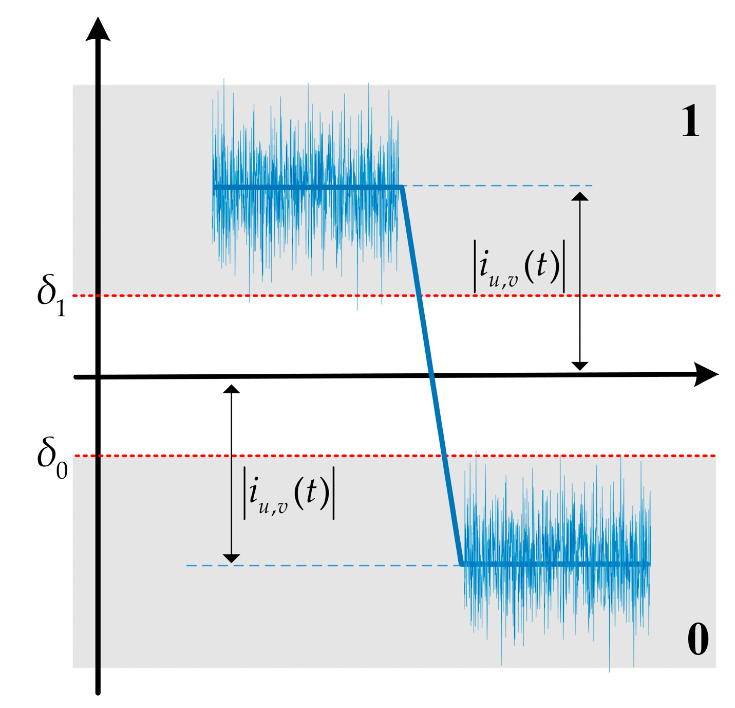
Figure 5.
Schematic diagram of the 0–1 judgment.
and here are the set thresholds for the 0–1 judgment. If , then is judged to be 1. If , then is judged to be 0.
Figure 5.
Schematic diagram of the 0–1 judgment.
and here are the set thresholds for the 0–1 judgment. If , then is judged to be 1. If , then is judged to be 0.
Figure 6.
Result of the frame synchronization code recognition: (a) no peak appeared if there was no frame synchronization code, and (b) a clear peak appeared if there was a frame synchronization code.
Figure 6.
Result of the frame synchronization code recognition: (a) no peak appeared if there was no frame synchronization code, and (b) a clear peak appeared if there was a frame synchronization code.
Figure 7.
DP-QPSK receiver performance with different delays in a back-to-back configuration: (a) Q factor versus DLI differential delay under a given optical signal-to-noise ratio (OSNR) of 15 dB, (b) the OSNR required for receivers with different DLI delays at the FEC (Forward Error Correction) threshold of BER = 3.8 × 10⁻³.
Figure 8.
Measured OSNR penalty versus the chromatic dispersion at BER = 3.8 × 10⁻³: (a) the dispersion tolerance due to the 2 dB OSNR penalty of the receiver, and (b) the OSNR penalty required for receivers with different delays to maintain a BER of 3.8 × 10⁻³ under the same system dispersion.
Figure 8.
Measured OSNR penalty versus the chromatic dispersion at BER = 3.8 × 10⁻³: (a) the dispersion tolerance due to the 2 dB OSNR penalty of the receiver, and (b) the OSNR penalty required for receivers with different delays to maintain a BER of 3.8 × 10⁻³ under the same system dispersion.
Table 1.
Correspondence between the phase difference and the demodulated symbols.
Table 1.
Correspondence between the phase difference and the demodulated symbols.
| 0 | | | |
|---|
| | | | |
| IQ | 11 | 01 | 00 | 10 |
Table 2.
Coded relationship between the input dual-bit symbols and the modulated phases.
Table 2.
Coded relationship between the input dual-bit symbols and the modulated phases.
| Dual-Bit Symbols | 00 | 01 | 11 | 10 |
|---|
| Phases of Mode A | 0 | | | |
| Phases of Mode B | | | | |
© 2020 by the authors. Licensee MDPI, Basel, Switzerland. This article is an open access article distributed under the terms and conditions of the Creative Commons Attribution (CC BY) license (http://creativecommons.org/licenses/by/4.0/).


