Light Load Efficient Silicon Power Converters Based on Wide Bandgap Circuit Extensions


Abstract
1. Introduction
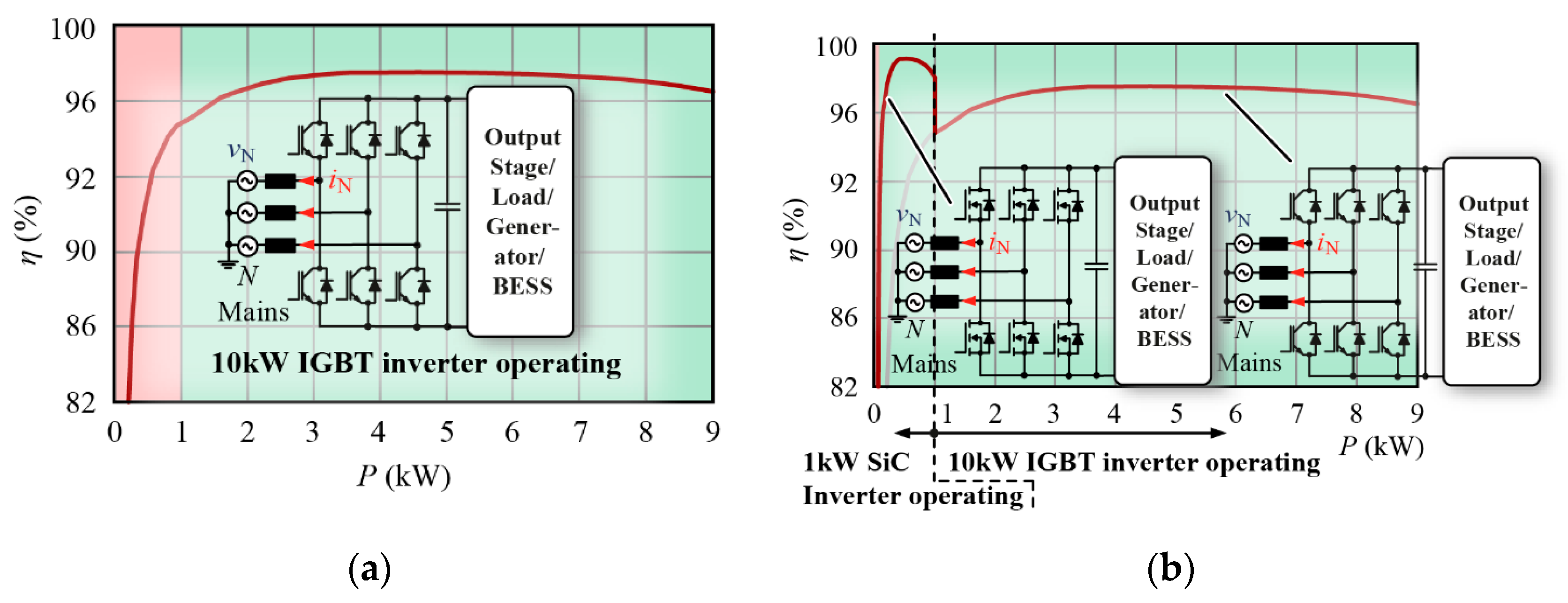
1.1. Background
1.2. Relevant Contribution to This Field
2. General Considerations
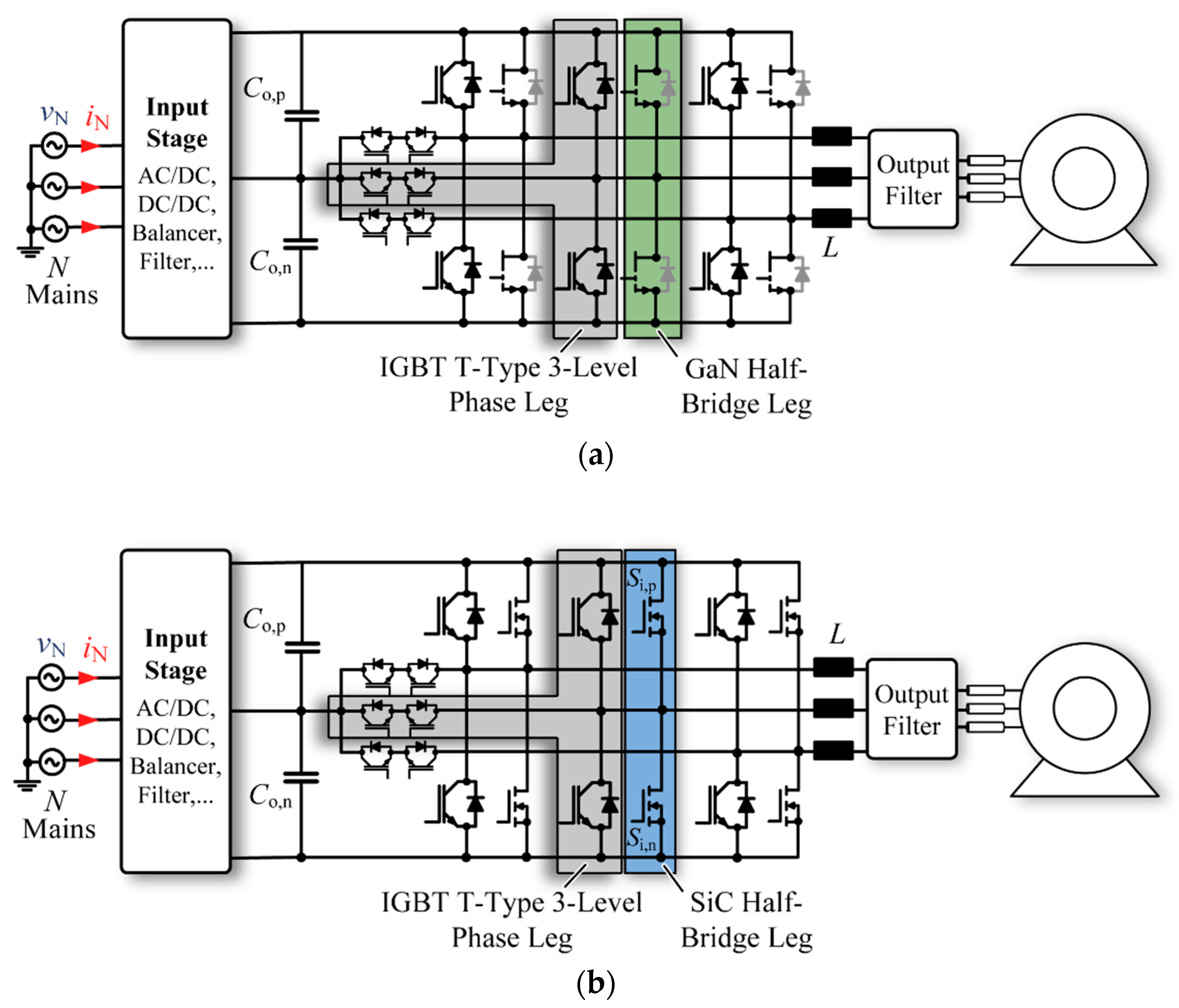
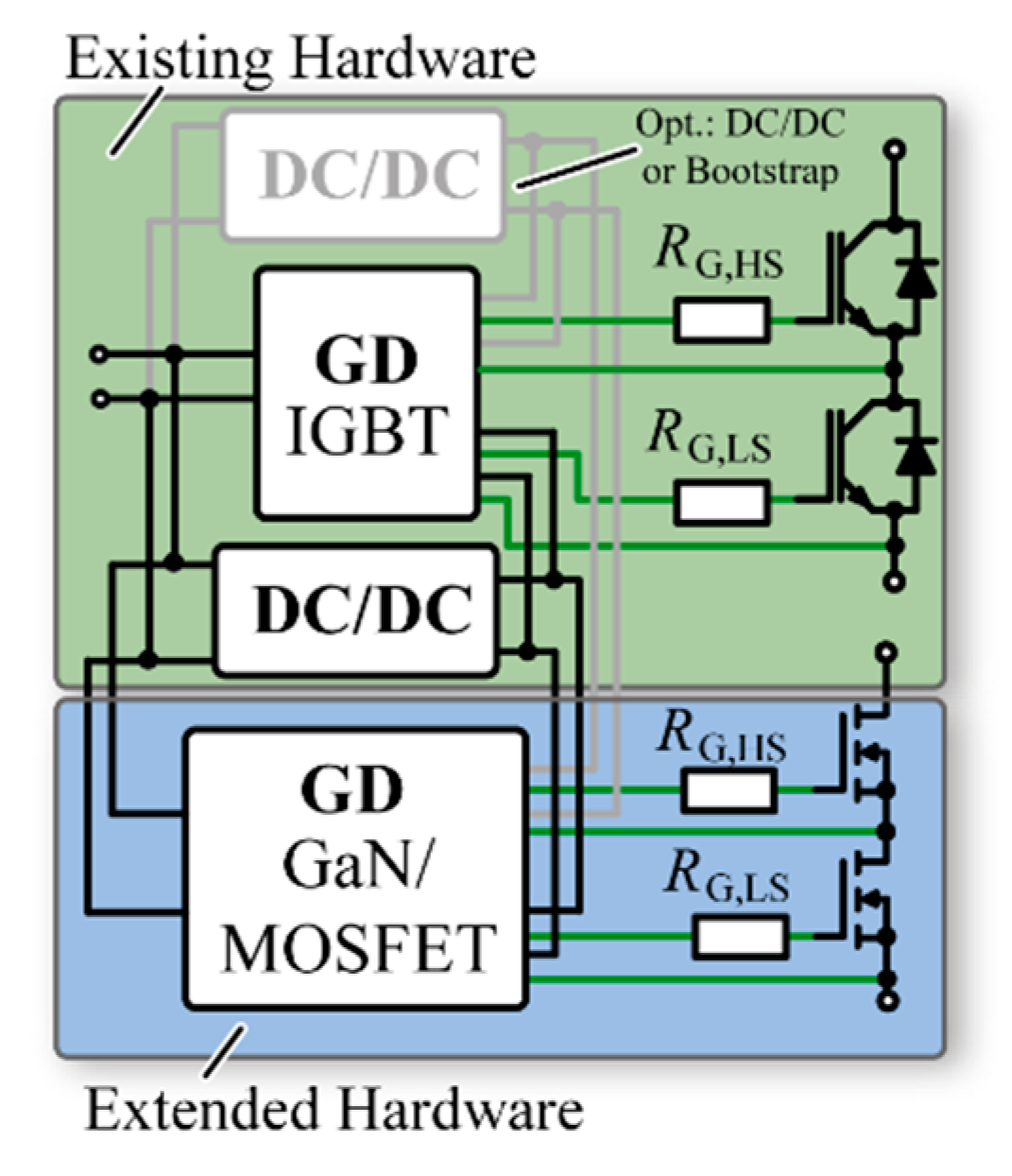
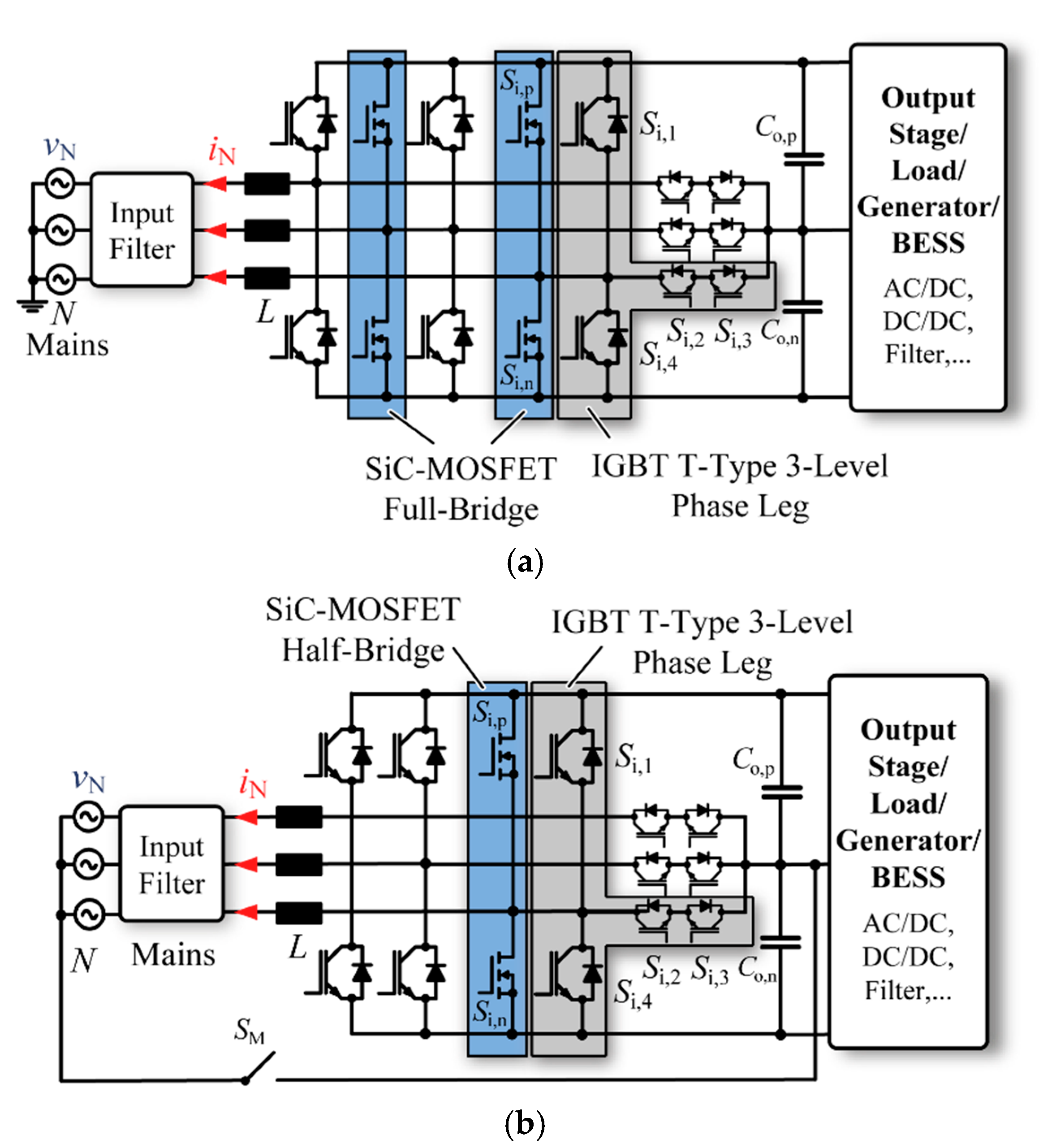
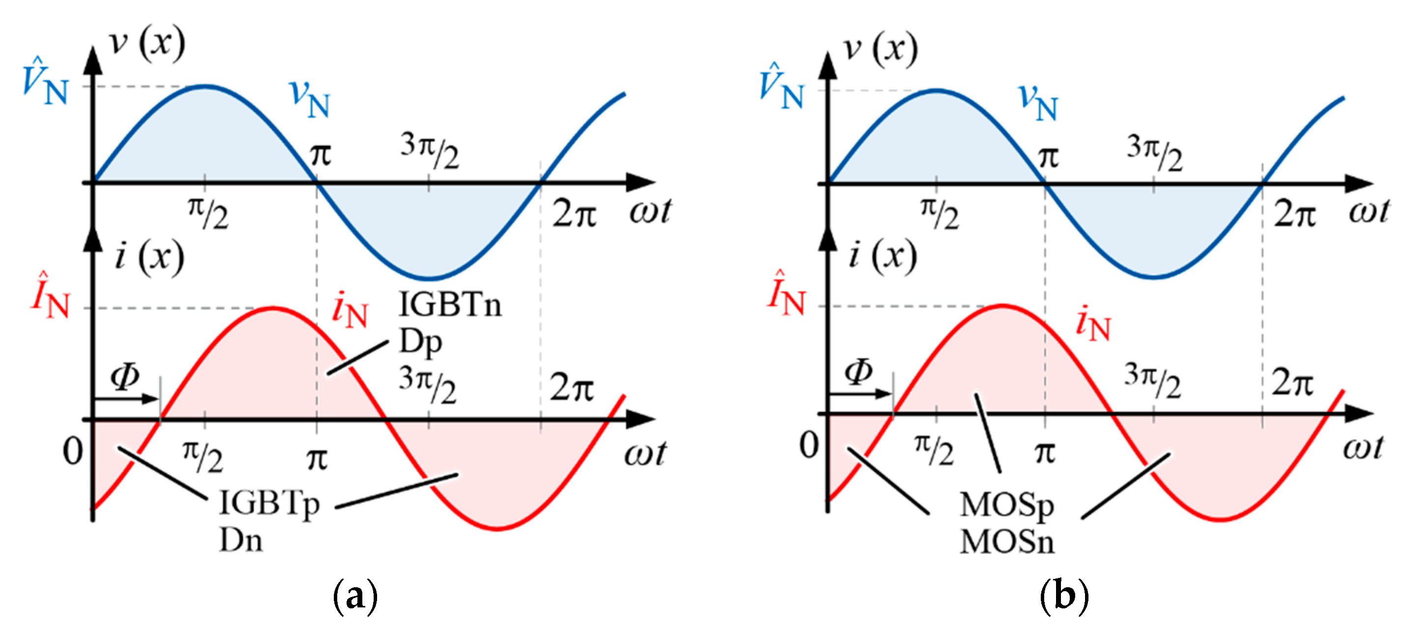
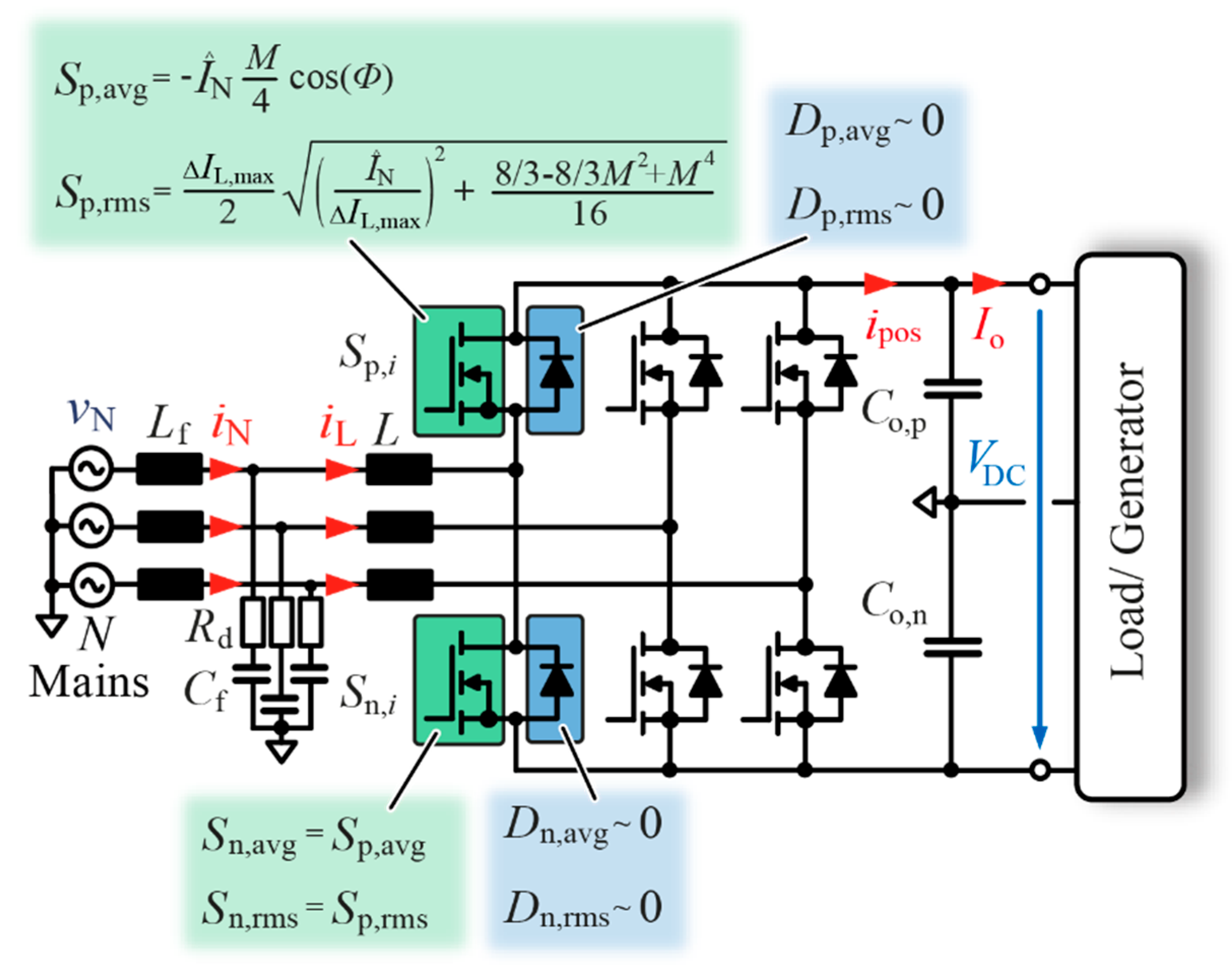
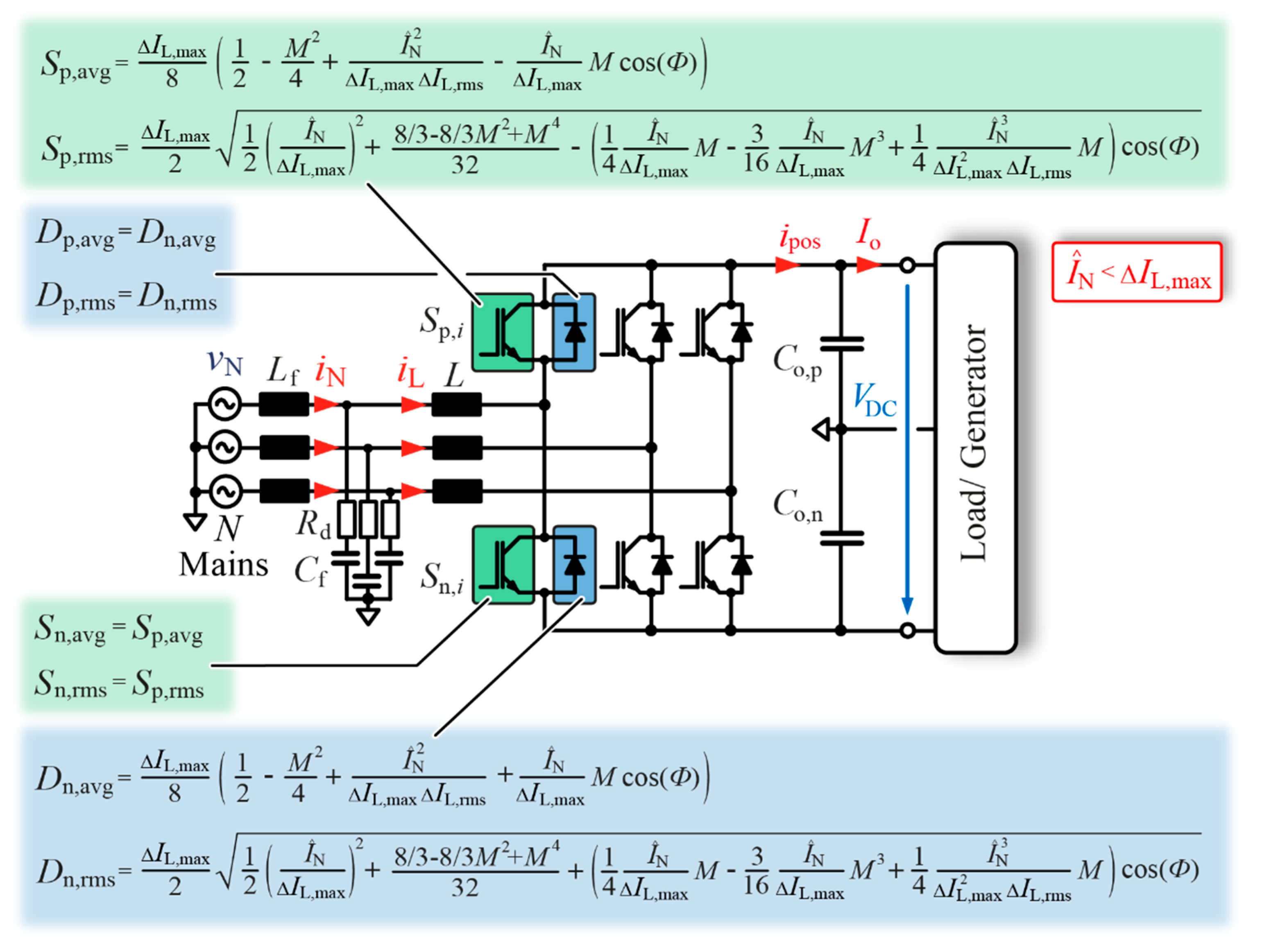
2.1. Topologies
2.2. General Design Strategy and Cost Optimization
2.3. Voltage Balancing of Multilevel Converters
3. Definition of Main Design Parameters for Three-Phase Six-Switch Converter Example
3.1. Pre-Design of 125 kW Grid-Connected Three-Phase Six-Switch Converter Stage
3.2. Pre-Design of 10 kW SiC Light-Load Converter Stage
3.3. Summary of Design Results
4. The Efficiency of Hybrid Power Stage under Light–Load Conditions
4.1. 125 kW Si IGBT Converter vs. 10 kW SiC Power Stage under Light-Load Conditions
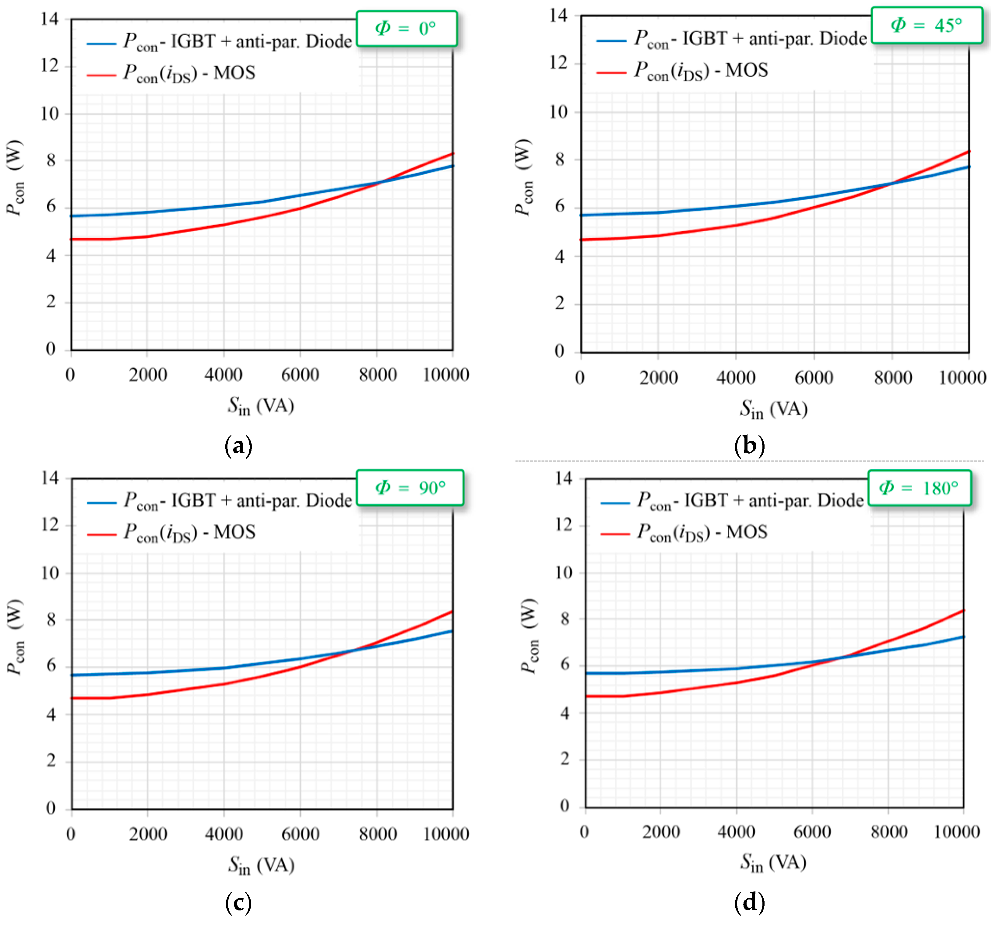
4.1.1. Conduction Losses of IGBT- and SiC-Based Light–Load Setup
4.1.2. Switching Losses of IGBT- and SiC-Based Light-Load Setup
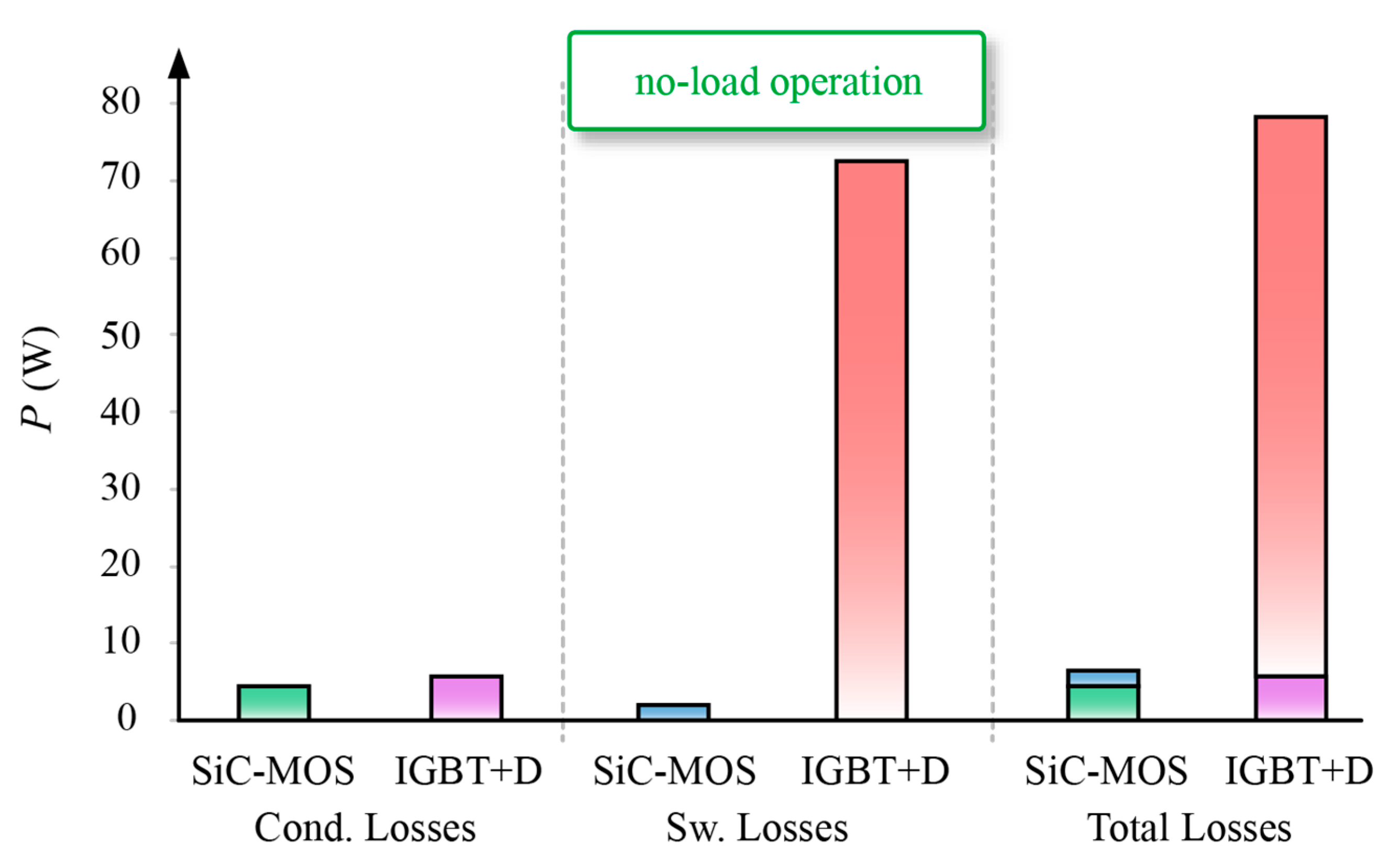
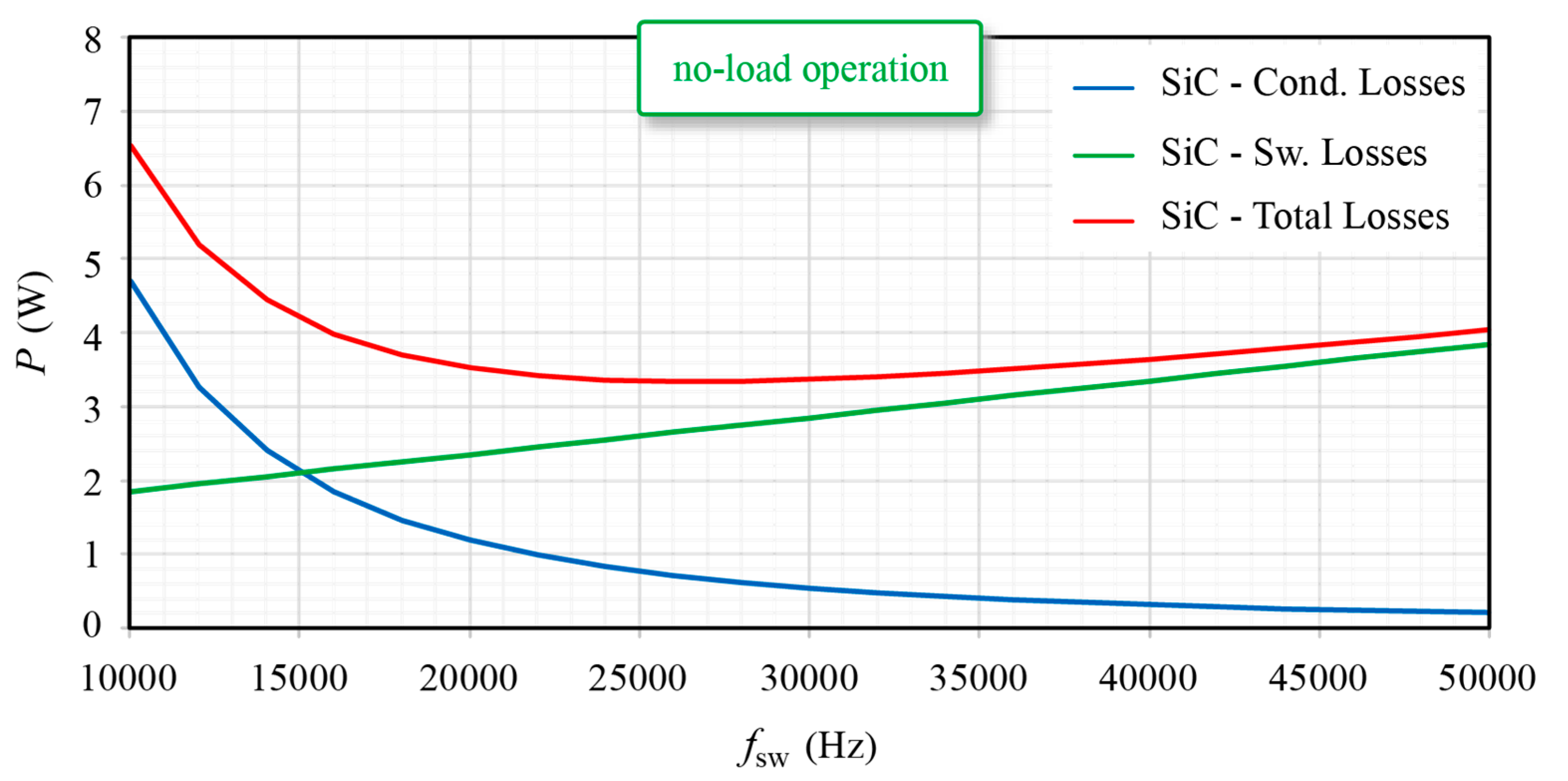
4.1.3. Total Semiconductor Loss-Overview and Optimization Prospects
4.2. Further Loss Improvements Due to GaN-Based WBG Technology
5. Conclusions
Author Contributions
Funding
Conflicts of Interest
Abbreviation
| Abbreviation | Meaning |
| AC | Alternating current |
| DC | Direct current |
| FFCS | Flywheel fast-charging system |
| GaN | Gallium nitride |
| GD | Gate driver |
| GHG | Greenhouse gas |
| IGBT | Insulated-gate bipolar transistor |
| MOSFET | Metal-oxide-semiconductor field-effect transistor |
| PV | Photovoltaic |
| PWM | Pulse-width modulation |
| ROHM | Rohm semiconductor corporation |
| SiC | Silicon carbide |
| SiC–MOSFET | Silicon carbide-metal oxide semiconductor field-effect transistor |
| Si–IGBT | Silicon-insulated-gate bipolar transistor |
| THD | Total harmonic distortion |
| WBG | Wide-bandgap |
| UPS | Uninterruptable power supply |
Nomenclature
| M | Modulation index |
| rms | Root mean square |
| avg | Average value |
| SN | Nominal apparent power |
| PN | Nominal active power |
| QN | Nominal reactive power |
| Psw | Semiconductor’s switching loss |
| Linv | Input inductance/phase |
| Dp | High-side diode |
| Dn | Low-side diode |
| IN,pk | Nominal peak current |
| IN,rms | Nominal rms current |
| IDS | Semiconductors cont. drain current |
| |∆ILmax| | Maximum of peak-to-peak input current ripple |
| |∆ILmin| | Minimum of peak-to-peak input current ripple |
| ∆IL,rms | Input current ripple rms |
| Io | Output current of the converter |
| VLL | Mains line-to-line voltage |
| VDC | Total DC-link voltage |
| VD | Diode forward voltage |
| VT | IGBT forward voltage |
| VDS | Transistor max. blocking voltage |
| Ron | On-resistance of semiconductors |
| RD | Equivalent resistance of antiparallel diode |
| fsw | Switching frequency |
| fN | Mains frequency |
| Φ | Phase angle |
| koff | Turn-off switching loss coefficient |
| ω | Angular frequency |
| t | Time |
| φ | ωt |
References
- Lao, J.; Tan, M.T. Design of a low swing power-efficient output stage for DC-DC converters. In Proceedings of the TENCON 2009-2009 IEEE Region 10 Conference, Singapore, 23–26 January 2009; pp. 1–6. [Google Scholar]
- El Bassiouny, O.A.; Dhople, S.V.; Davoudi, A.; Chapman, P.L. Energy-efficient cost-effective inverter configuration for residential photovoltaic systems. In Proceedings of the 2010 35th IEEE Photovoltaic Specialists Conference, Honolulu, HI, USA, 20–25 June 2010; pp. 400–406. [Google Scholar]
- Yu, R.; Pong, B.M.H.; Ling, B.W.-K.; Lam, J. Two-Stage Optimization Method for Efficient Power Converter Design Including Light Load Operation. IEEE Trans. Power Electron. 2012, 27, 1327–1337. [Google Scholar] [CrossRef]
- Agamy, M.S.; Harfman-Todorovic, M.; Elasser, A.; Chi, S.; Steigerwald, R.L.; Sabate, J.A.; McCann, A.J.; Zhang, L.; Mueller, F.J. An Efficient Partial Power Processing DC/DC Converter for Distributed PV Architectures. IEEE Trans. Power Electron. 2014, 29, 674–686. [Google Scholar] [CrossRef]
- Suntio, T.; Kuperman, A. Comments on “An Efficient Partial Power Processing DC/DC Converter for Distributed PV Architectures”. IEEE Trans. Power Electron. 2015, 30, 2372. [Google Scholar] [CrossRef]
- Gandhimathi, C. DC-DC converter with improved light load efficiency and transient response. In Proceedings of the 2013 International Conference on Communication and Signal Processing, Melmaruvathur, India, 3–5 April 2013; pp. 176–180. [Google Scholar]
- Luo, K.; Wang, H.; Gou, C.; Peng, K.; Yang, F.; Hu, Y. A Novel PWM/PFM Control Technique for Transient Improvement and High Efficiency Over a Wide Load Range in Buck DC-DC Converter. In Proceedings of the 2018 IEEE 3rd International Conference on Integrated Circuits and Microsystems (ICICM), Shanghai, China, 24–26 November 2018; pp. 169–173. [Google Scholar]
- Akca, H.; Selamogullari, U.S. Hybrid switch use for light load efficiency improvement of a power inverter for stand-alone residential renewable energy system. In Proceedings of the 15th European Conference on Power Electronics and Applications (EPE), Lille, France, 2–6 September 2013; pp. 1–6. [Google Scholar]
- Chen, Z.; Wu, H.; Sun, K.; Ni, L.; Xing, Y. Light-load efficiency optimization for module integrated converters in photovoltaic systems. In Proceedings of the IEEE Energy Conversion Congress and Exposition, Denver, CO, USA, 15–19 September 2013; pp. 5560–5565. [Google Scholar]
- Koo, K.-W.; Kwak, C.-H.; Kim, D.-H.; Lee, B.-K. Improved operation algorithm for parallel three phase PWM converter at light load conditions. In Proceedings of the 18th International Conference on Electrical Machines and Systems (ICEMS), Pattaya City, Thailand, 25–28 October 2015; pp. 432–435. [Google Scholar]
- Othman, A.M.; Gabbar, H.A. Enhanced Microgrid Dynamic Performance Using a Modulated Power Filter Based on Enhanced Bacterial Foraging Optimization. Energies 2017, 10, 776. [Google Scholar] [CrossRef]
- Gabbar, H.A.; Othman, A.M. Performance optimisation for novel green plug-energy economizer in micro-grids based on recent heuristic algorithm. Transm. Distrib. IET Gener. 2016, 10, 678–687. [Google Scholar] [CrossRef]
- Gabbar, H.A.; Othman, A.M.; Pino, F.; Repetto, M. Improved Performance of Flywheel Fast Charging System (FFCS) Using Enhanced Artificial Immune System (EAIS). IEEE Syst. J. 2020, 14, 824–831. [Google Scholar] [CrossRef]
- Ertl, H.; Wiesinger, T.; Kolar, J.W. Active voltage balancing of DC-link electrolytic capacitors. IET Power Electron. 2008, 1, 488–496. [Google Scholar] [CrossRef]
- Device Application Fuji IGBT Modules for Solar Inverter. Available online: https://www.fujielectric.com/products/semiconductor/usage/box/doc/pdf/Solar_inverter_(ver5).pdf (accessed on 4 June 2020).
- FF600R12KE4—Datasheet—Infineon Technologies. Available online: https://www.infineon.com/cms/en/product/power/igbt/igbt-modules/ff600r12ke4/ (accessed on 4 June 2020).
- AG, I.T. IMZ120R030M1H—Datasheet—Infineon Technologies. Available online: https://www.infineon.com/cms/en/product/power/mosfet/silicon-carbide/discretes/imz120r030m1h/ (accessed on 4 June 2020).
- GS66508T—Datasheet—GaN Systems. Available online: https://gansystems.com/gan-transistors/gs66508t/ (accessed on 4 June 2020).
- Application Notes—GaN Systems. Available online: https://gansystems.com/design-center/application-notes/ (accessed on 4 June 2020).
- 650V, 30A, THD, Trench-Structure, Silicon-Carbide (SiC) MOSFET-SCT3080AL. Available online: https://www.rohm.com/products/sic-power-devices/sic-mosfet/sct3080al-product (accessed on 4 June 2020).
- Application Note ROHM SiC Power Devices and Modules. Available online: https://fscdn.rohm.com/en/products/databook/applinote/discrete/sic/common/sic_appli-e.pdf (accessed on 4 June 2020).
- Koaxialshunts—Application Notes. Available online: http://www.ib-billmann.de/koax.php#apnot (accessed on 4 June 2020).
- Coaxial Shunts T&M RESEARCH PRODUCT. Available online: http://www.ib-billmann.de/bilder/pdf/shunts_tech.pdf (accessed on 4 June 2020).


| Design Parameter | Value |
|---|---|
| Mains voltage: | VLL = 400 Vrms |
| Mains frequency | fN = 50 Hz |
| Total DC-link voltage | VDC = 800 V |
| Nominal power | SN = PN = 125 kW |
| Design Parameter | Value |
|---|---|
| Switching frequency Si/SiC | fsw = 10 kHz |
| Input inductance/phase: | Linv = 250 µH |
| Input current ripple maximum | |∆ILmax| = 80 A |
| Input current ripple minimum | |∆ILmin| = 27 A |
| Input current ripple rms | ∆IL,rms = 56.7 A |
| IGBT module (3ph./125 kW) | FF600R12KE4 1200 V/600 A |
| SiC MOSFET (3ph./10 kW) | IMZ120R030M1H 1200 V/30 mΩ |
| Parameter | Value |
|---|---|
| MOSFET on resistance: | Ron,MOS = 35 mΩ |
| IGBT forward voltage (light-load): | VT = 0.7 V |
| IGBT on resistance (light-load): | Ron,IGBT = 4.2 mΩ |
| IGBT anti-p. diode forward voltage (light-load): | VD = 0.85 V |
| IGBT anti-p. diode on resistance (light-load): | Ron,IGBT = 3.5 mΩ |
| Φ (°) | Sin (kVA) | IIGBT,avg (A) | IIGBT,rms (A) | ID,avg (A) | ID,rms (A) | IMOS,rms (A) | PIGBT,avg (W) | PIGBT,rms (W) | PD,avg (W) | PD,rms (W) | PMOS (W) |
|---|---|---|---|---|---|---|---|---|---|---|---|
| 0 | 0 | 3.35 | 8.19 | 3.35 | 8.19 | 11.6 | 2.34 | 0.28 | 2.84 | 0.23 | 4.69 |
| 0 | 5000 | 2.54 | 7.63 | 4.62 | 10.11 | 12.7 | 1.78 | 0.24 | 3.93 | 0.36 | 5.61 |
| 0 | 10,000 | 2.19 | 8.36 | 6.36 | 13.01 | 15.5 | 1.53 | 0.29 | 5.4 | 0.59 | 8.37 |
| 180 | 0 | 3.35 | 8.19 | 3.35 | 8.19 | 11.6 | 2.34 | 0.28 | 2.84 | 0.23 | 4.69 |
| 180 | 5000 | 4.62 | 10.11 | 2.54 | 7.63 | 12.7 | 3.23 | 0.43 | 2.16 | 0.20 | 5.61 |
| 180 | 10,000 | 6.36 | 13.01 | 2.19 | 8.36 | 15.5 | 4.45 | 0.71 | 1.86 | 0.24 | 8.37 |
| Parameter | Value |
|---|---|
| koff,MOS (800 V, 2 Ω, 50 °C) | 5 µJ/A |
| doff,MOS (800 V, 2 Ω, 50 °C) | 50 µJ |
| koff,IGBT (800 V, 0.63 Ω, 50 °C) | 120 µJ/A |
| doff,IGBT (800 V, 0.63 Ω, 50 °C) | 4 mJ |
| Psw,MOS (800 V, 2 Ω, 50 °C, 10 kHz)—no load | 1.84 W |
| Psw,IGBT (800 V, 0.63 Ω, 50 °C, 10 kHz)—no load | 72.6 W |
| Parameter | Value |
|---|---|
| SiC–MOSFET on resistance: | Ron,MOS = 80 mΩ |
| SiC–MOSFET max. blocking voltage | VDS,max = 650 V |
| SiC–MOSFET cont. drain current (TC = 25 °C) | IDS,25 °C = 30 A |
| GaN transistor on resistance: | Ron,GaN = 50 mΩ |
| GaN transistor max. blocking voltage | VDS,max = 650 V |
| GaN transistor cont. drain current (TC = 25 °C) | IDS,25 °C = 30 A |
© 2020 by the authors. Licensee MDPI, Basel, Switzerland. This article is an open access article distributed under the terms and conditions of the Creative Commons Attribution (CC BY) license (http://creativecommons.org/licenses/by/4.0/).
Share and Cite
Makoschitz, M.; Biswas, S. Light Load Efficient Silicon Power Converters Based on Wide Bandgap Circuit Extensions. Appl. Sci. 2020, 10, 4730. https://doi.org/10.3390/app10144730
Makoschitz M, Biswas S. Light Load Efficient Silicon Power Converters Based on Wide Bandgap Circuit Extensions. Applied Sciences. 2020; 10(14):4730. https://doi.org/10.3390/app10144730
Chicago/Turabian StyleMakoschitz, Markus, and Sumanta Biswas. 2020. "Light Load Efficient Silicon Power Converters Based on Wide Bandgap Circuit Extensions" Applied Sciences 10, no. 14: 4730. https://doi.org/10.3390/app10144730
APA StyleMakoschitz, M., & Biswas, S. (2020). Light Load Efficient Silicon Power Converters Based on Wide Bandgap Circuit Extensions. Applied Sciences, 10(14), 4730. https://doi.org/10.3390/app10144730