Article

Thermal Mapping of Power Semiconductors in H-Bridge Circuit †

1
Department of Energy Technology, Aalborg University, 9220 Aalborg, Denmark
2
Department, Schneider Electric Power Drives GmbH, 1210 Vienna, Austria
*
Author to whom correspondence should be addressed.
This paper is an extended version of paper published in 13th IEEE International Conference on Compatibility, Power Electronics, and Power Engineering (IEEE CPE-POWERENG 2019) held in Soenderborg, Denmark, 23–25 April 2019.
Appl. Sci. 2020, 10(12), 4340; https://doi.org/10.3390/app10124340
Submission received: 30 April 2020 / Revised: 29 May 2020 / Accepted: 8 June 2020 / Published: 24 June 2020
(This article belongs to the Special Issue Advancing Grid-Connected Renewable Generation Systems 2019)

Abstract

:
In this paper, a universal H-bridge circuit is used as a loading emulator to investigate the loss and thermal models of the power semiconductor. Based on its operation principle and modulation method, the dominating factors’ (e.g., power factor, loading current, fundamental frequency, and switching frequency) impact on the thermal stress of power semiconductors is considerably evaluated. The junction temperature in terms of the mean value and its swing is verified by using Piecewise Linear Electrical Circuit Simulation (PLECS) simulation and experimental setup. It helps to allocate the loading condition in order to obtain the desired thermal stress.

1. Introduction

Reliability and lifetime prediction of power converters have been a major research topic in the last few decades, especially for locomotives, high-power drives, electric vehicles, and renewable energy applications [1,2,3]. According to an industrial survey presented in [4], power semiconductor failures are a dominant concern for the reliability of power converters. The main failures in power semiconductors are caused by thermo-mechanical fatigue, and thus thermal analysis of the power converter is essential for reliability testing in various applications.
Temperature cycling and power cycling are the two most common thermal acceleration approaches used in assessing the reliability of the power device [5]. In temperature cycling, components are periodically moved between cooling and heating chambers, where components are passively heated up. During the power cycling, components are actively heated up by losses produced in the power semiconductor and cooled down with the aid of cooling equipment. For the dc power cycling, a constant dc current for a continuous period of time is considered in a dc circuit, which is simple and easy for monitoring parameters. A specified load current is periodically applied to the insulated gate bipolar transistor (IGBT), and the lower and higher temperature limits are the parameters to be set initially by means of adjusting the loading current, turn-on and turn-off period and cooling system [6,7]. This is one of the standard testing circuits, which ensures faster changes in temperature due to the higher power losses. However, only the conduction loss is generated in this method, which is inconsistent with the properties of these fast-switching power devices.
For the ac power cycling, a Pulse-Width Modulation (PWM) switching sequence is applied for a time until the IGBT rises to the maximum temperature, and the device is switched off until it cools down to the minimum temperature [8,9,10]. As described in [10], a motor drive test circuit is established, and a short period of overload current is applied to generate the high-temperature variation. Although the failures are accelerated and occur in a low testing duration, the test is not as cost-effective, since the fatigue issues of the motor and other electrical components exist simultaneously. The back-to-back inverter configuration is proposed with an inductor in order to emulate the traction application [11]. With this arrangement, the system current is made to circulate between the two inverters so that each can operate at their full power. Only the conduction and switching losses of the power devices are provided by the dc power supply.
Even though the standard dc and ac testing methods can achieve the same thermal stress of the power device, the heating source is different due to the fact that the switching loss only exists in ac power cycling, which may result in various failure mechanisms of the power device. As the ac power cycling mimics realistic conditions of the power devices and emulates various applications by reconfiguring control objectives of the testing and loading legs [12], some research efforts are devoted to the H-bridge testing circuit [13,14,15,16,17,18]. In the real application, as the power device is normally selected with around two times the current margin, it makes the power device quite robust and will take years of time before the wear-out aging occurs. In contrast, if the H-bridge circuit is selected, the loading current through the device can be equal or even higher than the maximum loading current, which accelerates device aging much sooner. However, the operation principle of this circuit has not been well described. Moreover, the relationship between the loading condition and the junction temperature of the power semiconductor is not accurately established. In order to fill this research gap, the loss dissipation and thermal stress of the power devices are investigated in detail in this paper. The dominant factors (e.g., power factor, current amplitude, fundamental frequency, switching frequency) are considered, which can serve as the guideline of the loading condition for the desired thermal stress.
The rest of the paper is organized as follows. Section 2 introduces the basic operation principle of the H-bridge circuit. The loss and thermal models of the power semiconductor are described in Section 3. Section 4 verifies the loss dissipation and junction temperature in both the simulation and experimental setup. Some conclusions are drawn in Section 5.

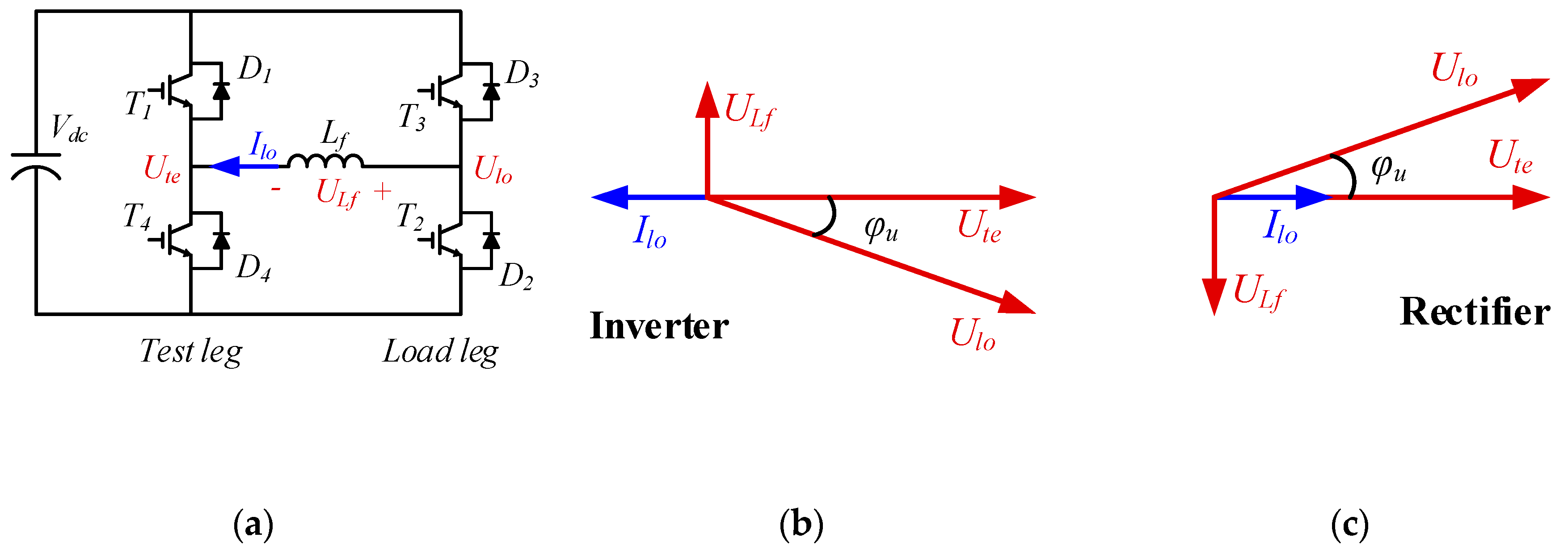
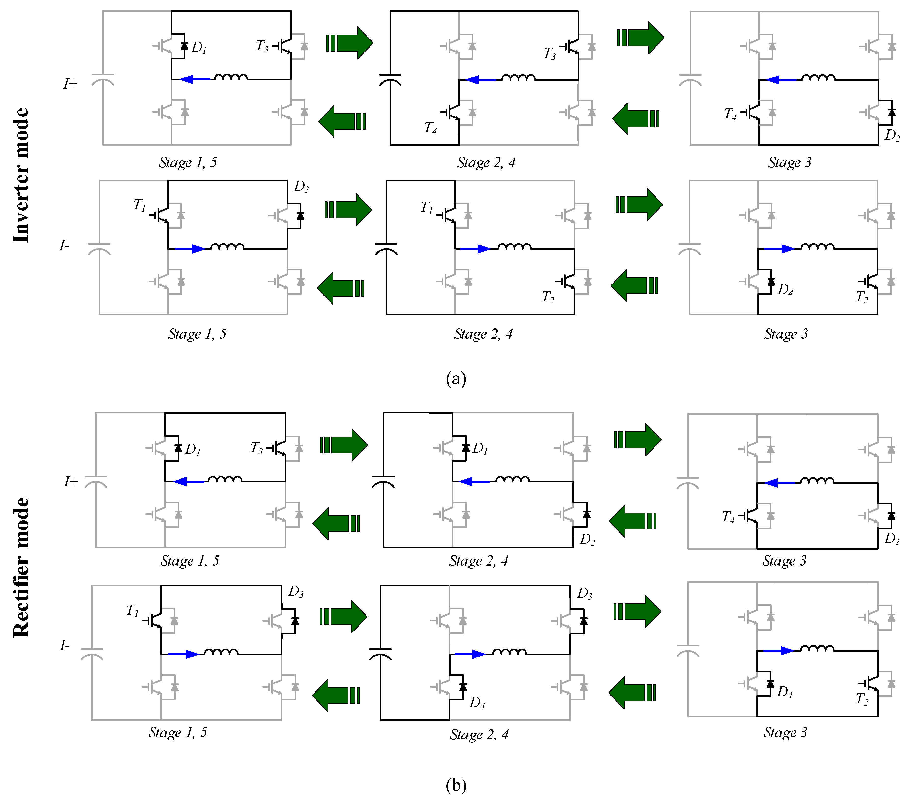
2. Operation Principle of H-Bridge Circuit

For the grid-tied converter used in renewable energy systems, the loading of the power devices is dominated by the grid requirements (e.g., active and reactive power). In respect to the power converter applied in generator/motor control, the generated current is tightly dependent upon the machine characteristic. Thus, regardless of the converter applications, its loading can simply be considered as a controlled current source.
A single-phase H-bridge circuit is shown in Figure 1a, which consists of a test leg and a load leg. An inductor in between is needed for the circuit operation. The test leg provides the reference voltage, while the load leg imitates the loading feature, supplying resistive, inductive or capacitive loading conditions. Consequently, the current flowing through the test leg can be regulated freely. According to the Kirchhoff voltage law, the relationship between the output voltage of the test leg U t e ¯ and the load leg U l o ¯ can be found as:
U t e ¯ = U l o ¯ + U L f ¯
where U L f ¯ is the voltage drop across the filter inductor Lf.
For typical operation conditions, the converter under the inverter mode and the rectifier mode are shown in Figure 1b,c. In the case of the inverter mode, the loading current Ilo is in the opposite direction to the reference voltage Ute. The amplitude of the load voltage Ulo becomes slightly higher and lags the reference voltage with φu. Similarly, in the case of the rectifier mode, the loading current is in phase with the reference voltage, which results in the leading load voltage.
According to the modulation scheme of the test and load legs in [18], the switching period can be divided into five stages. As shown in Figure 2, the activation status of power switches is described in detail, where both the positive and negative currents are considered. For the inverter mode, it is obvious that T1 and T4 conduct depending on the direction of loading current. Besides, the inductor current increases in stages 2 and 4, but it maintains the same in the rest of the period. Similarly, the loading current flowing through the power devices during rectifier mode is presented in Figure 2b. At different directions of the loading current, the conducting devices change to the complementary switches at all stages.
Regardless of the current direction, it is evident that the turn-on and turn-off loss of the IGBT, and reverse-recovery loss of the diode happen once during a switching period. Moreover, in the case of the inverter mode, the IGBTs T1 and T4 are primarily conducting. However, in the case of the rectifier mode, the diodes D1 and D4 conduct mainly. Consequently, the conduction loss is dominated by the IGBT in the inverter mode but by the diode in the rectifier mode.

3. Loss Dissipation and Junction Temperature of Power Devices

By knowing the current distribution between the IGBT and freewheeling diode within a fundamental period, their loss dissipation can be calculated analytically. According to the thermal impedance of the power devices and cooling method, the junction temperature can be estimated as well.

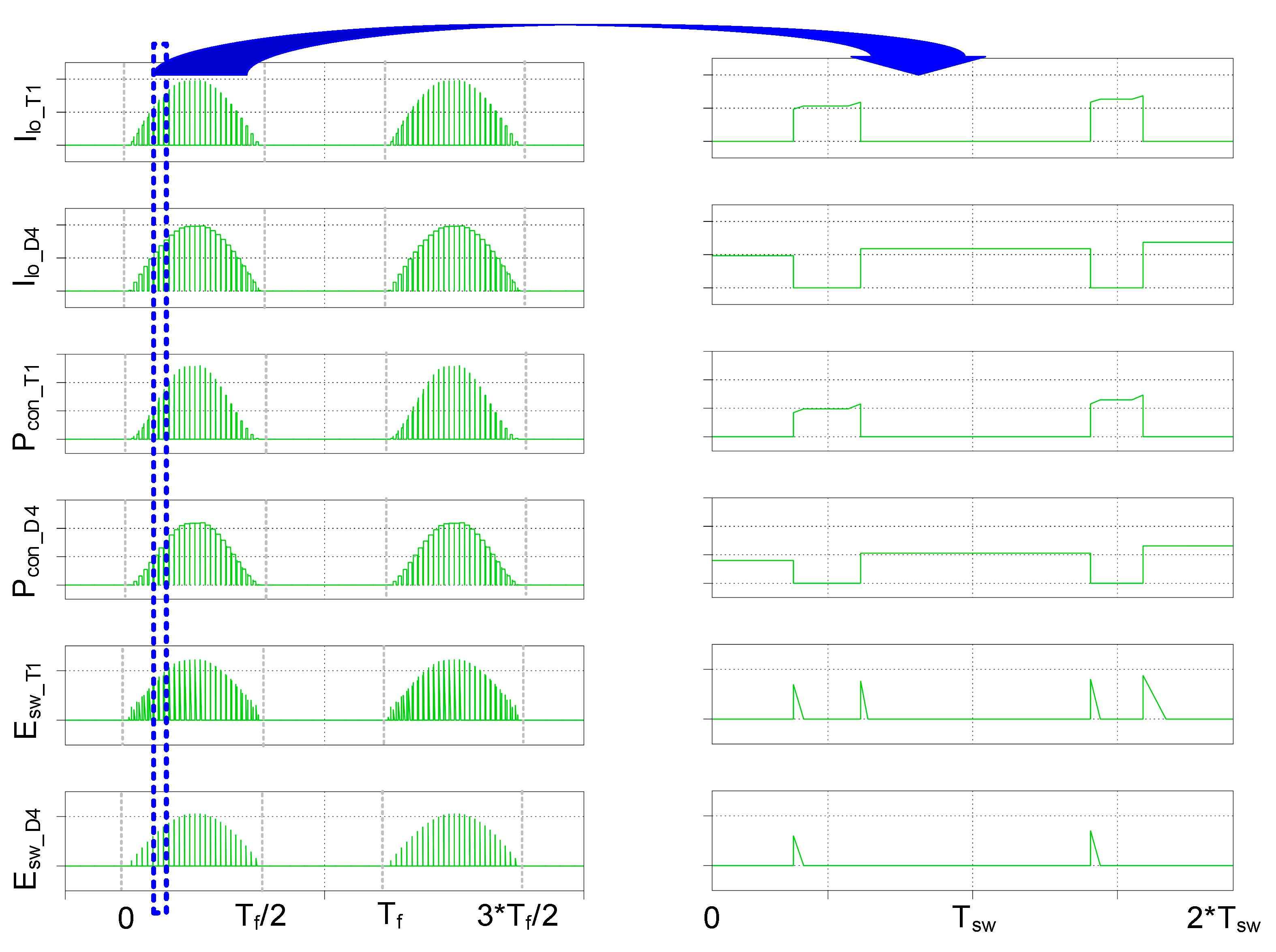
3.1. Loss Dissipation

As the power loss is symmetrically distributed among the upper and lower switches in the two-level power converter, the upper IGBT T1 and lower diode D4 are selected as an example. Under the steady-state operation, the loading current flowing through the upper IGBT T1 and lower diode D4 is described in Figure 3. It is noted that Ilo_T and Ilo_D indicate the loading current through the IGBT and diode, Pcon_T and Pcon_D indicate the power loss of the IGBT and diode, and Esw_T and Esw_D indicate the switching energy for the IGBT and diode, respectively. Due to the direction of the loading current, both the IGBT and the diode conducts only half of the fundamental period Tf. Within a switching period Tsw, as the loading current commutes from D4 to T1 once, the conduction losses and switching losses are generated in both the IGBT and the diode. Due to the fact that the sinusoidal loading current induces different dissipations in every switching period, the average power loss can be calculated, which is accumulated from each switching pattern during a fundamental period.
The conduction loss of the IGBT Pcon_T can be calculated as,
P c o n _ T = 1 T f 0 T f 2 V C E ( t ) i l o ( t ) d ( t ) d t
where Tf denotes the fundamental period, VCE denotes the on-state voltage of the IGBT, ilo denotes the loading current, and d denotes the duty cycle.
Considering the displacement angle between the loading current and modulated voltage φu, and making a linear approximation of the IGBT forward characteristics (initial on-state voltage drop VCE0 and equivalent resistor rCE), the conduction loss of the IGBT can be deduced by [19],
P c o n _ T = 1 2 ( 1 π V C E 0 I m + 1 4 r C E I m 2 ) + M cos φ u ( 1 8 V C E 0 I m + 1 3 π r C E I m 2 )
where Im denotes the amplitude of the loading current, and M denotes the modulation index, which equals the converter output voltage over half of the dc-bus voltage.
Similarly, the conduction loss of the diode Pcon_D can be calculated as,
P c o n _ D = 1 T f 0 T f 2 V F ( t ) i l o ( t ) ( 1 d ( t ) ) d t
where VF denotes the on-state voltage of the freewheeling diode. It can be noted that the lower diode conducts if its driving signal is high.
Assuming the linear approximation of the diode forward characteristics (initial on-state voltage drop VF0 and equivalent resistor rF), the conduction loss of the diode can be deduced by,
P c o n _ D = 1 2 ( 1 π V F 0 I m + 1 4 r F I m 2 ) M cos φ u ( 1 8 V F 0 I m + 1 3 π r F I m 2 )
As the turn-on energies Eon and turn-off energies Eoff of the IGBT can be described as a polynomial function [20], where aT denotes the zero-polynomial term, bT denotes the linear term, and cT denotes the quadratic term,
E s w _ T ( t ) = E o n ( t ) + E o f f ( t ) = V d c V d c * ( a T + b T I m ( t ) + c T I m 2 ( t ) )
the switching loss PswT can be calculated within a fundamental period,
P s w _ T = 1 T f E s w T ( i ) = f s w V d c V d c * ( a T 2 + b T π I m + c T 4 I m 2 )
where fsw denotes the switching frequency, Vdc denotes dc-bus voltage, and Vdc* denotes the dc-bus voltage under the testing condition.
Similarly, the recovery energy of the diode Err can be described as a polynomial function,
E s w _ D ( t ) = E r r ( t ) = V d c V d c * ( a D + b D I m ( t ) + c D I m 2 ( t ) )
The switching loss of the diode PswD can be deduced as follows,
P s w _ D = 1 T f E s w D ( i ) = f s w V d c V d c * ( a D 2 + b D π I m + c D 4 I m 2 )

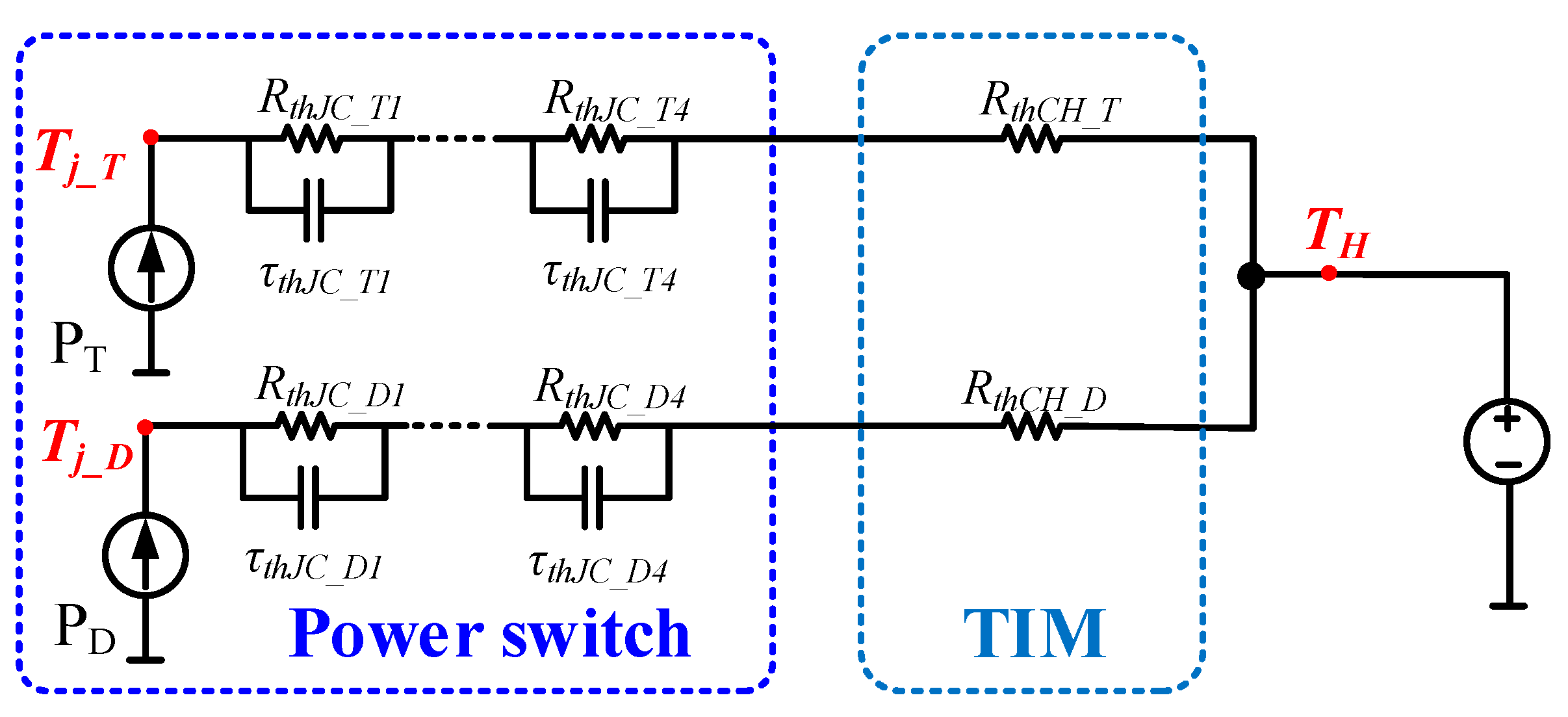
3.2. Junction Temperaute Estimation

The thermal stress of the power devices is usually determined by the thermal parameters of the power module itself (from junction to case), the Thermal Interface Material (TIM), and the cooling method. A typical thermal model of the power module is graphically depicted in Figure 4. It can be seen that the power switches share the common cooling system, since these power devices are located in the same housing of the IGBT module.
Generally, the thermal time constant of the cooling system is from dozens of seconds to hundreds of seconds, while the thermal time constant of the power device is hundreds of milliseconds. On the other hand, the maximum fundamental period of the converter current is around several seconds, which implies that the thermal cycling caused by the cooling can almost be neglected [21,22]. As a result, for the steady-state analysis, the thermal model of the cooling method will only affect the mean junction temperature, but has no effect on the junction temperature fluctuation.
Consequently, the mean junction temperature Tjm can be calculated as,
T j m _ T / D = P T / D ( i = 1 4 R t h J C _ T / D ( i ) + R t h C H _ T / D ) + T H
Within a fundamental period, the junction temperature fluctuation is caused by half-cycle conduction and half-cycle blocking of the power semiconductor. Assuming the periodic pulse power loss, the junction temperature fluctuation dTj can be calculated as [19],
d T j _ T / D = 2 P T / D i = 1 4 R t h J C _ T / D ( i ) ( 1 e t o n τ t h J C _ T / D ( i ) ) 2 1 e t p τ t h J C _ T / D ( i )
In Equation (10), RthJC, RthCH denote the thermal resistance from the junction to case of the power module, and the TIM, respectively. Subscripts T and D denote the IGBT and the freewheeling diode, where subscripts i denotes a four-layer Foster structure for the power module. P is the power loss of each power semiconductor, and TH is the heatsink temperature. In Equation (11), tp denotes the fundamental period of the current, ton denotes a half of fundamental period, and τ denotes the thermal time constant of each Foster layer.

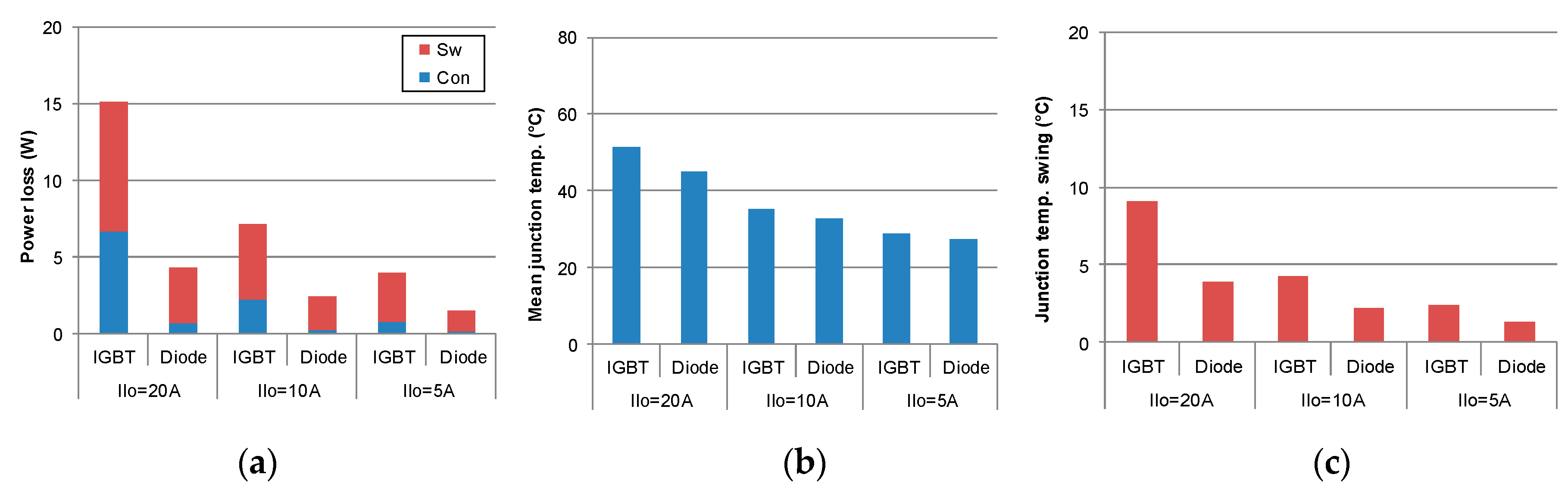
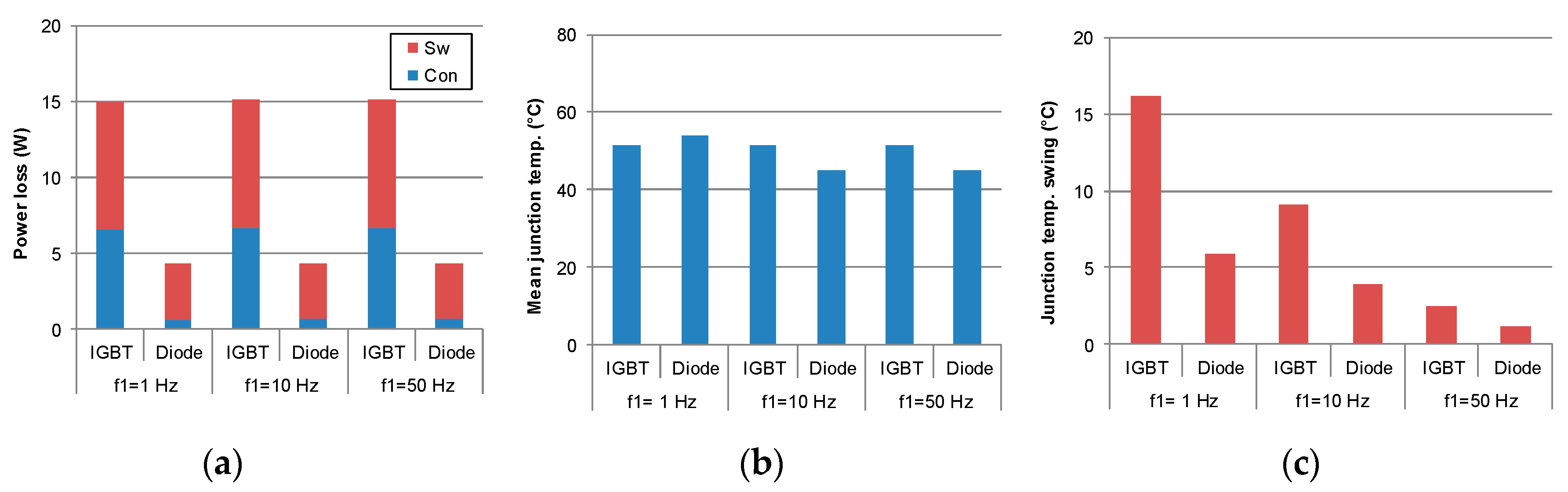
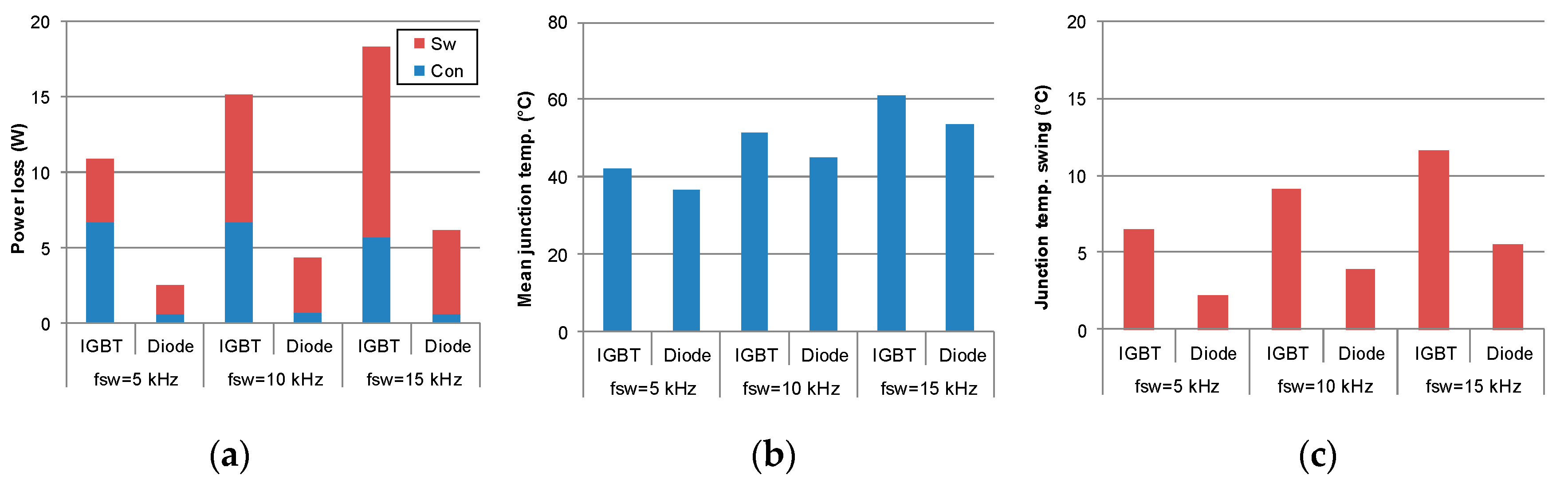
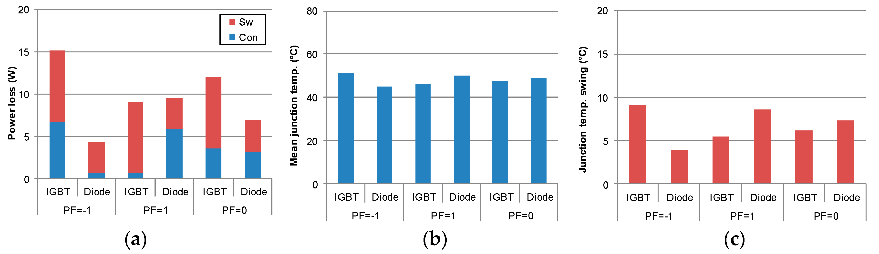
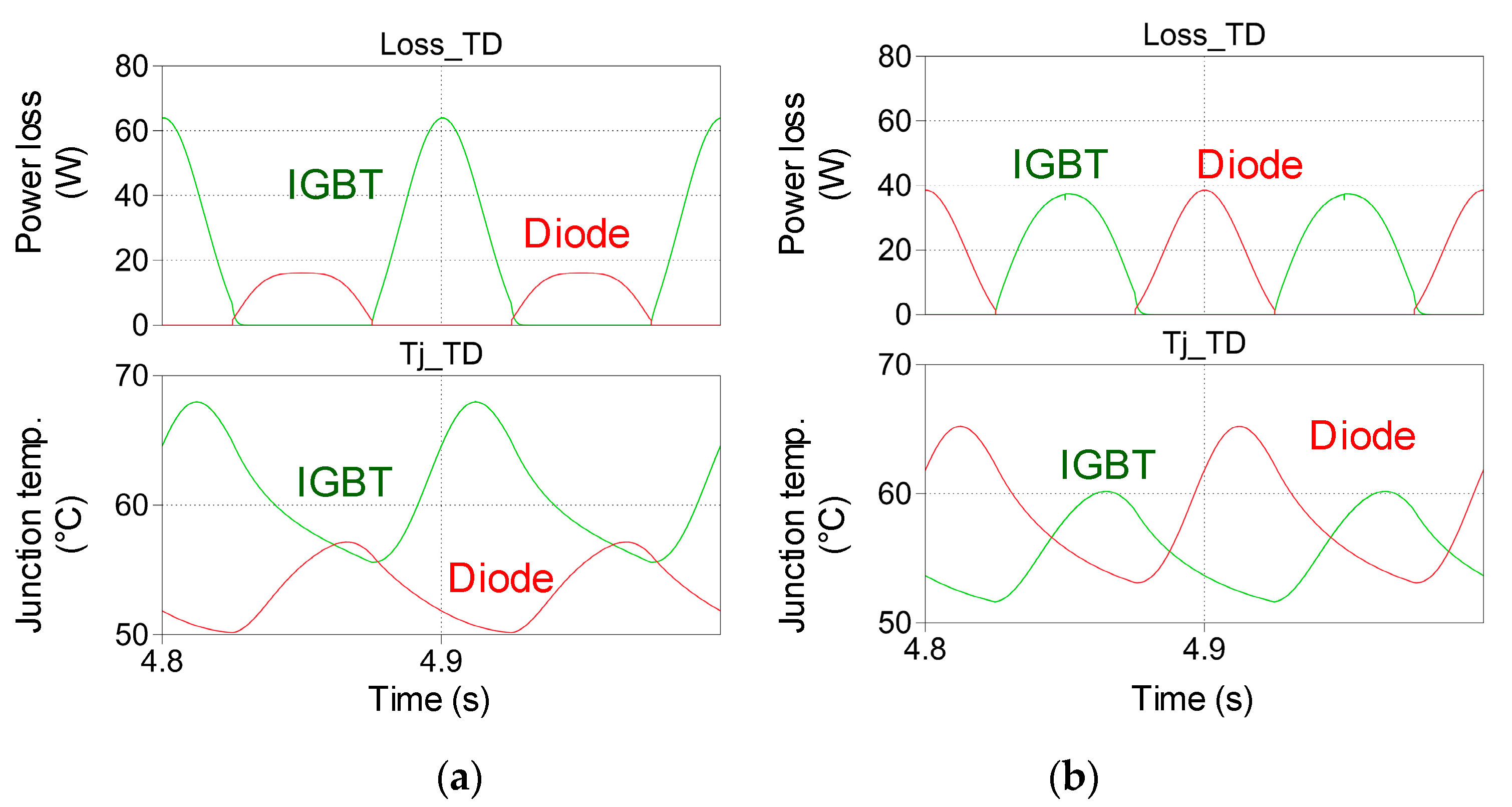
4. Thermal Stresses of Power Devices at Various Loading Conditions

In this section, the factors that affect the thermal loading of the power devices are investigated. Then, their loss dissipation and thermal stresses are analytically calculated and compared with the simulation and experimental results.

4.1. Dominating Factors for Device Loading

The key parameters of the power converter are listed in Table 1, where a 1200 V/50 A power module with a maximum junction temperature of 150 °C is selected for both the test and load legs [23]. The converter under the inverter mode, i.e., the Power Factor (PF) equals −1, is regarded as the rated condition. Moreover, the rated current, fundamental frequency, and switching frequency are summarized in Table 1 as well. The rated peak current of 20 A and the dc-link voltage of 400 V are selected in order to leave the sufficient current and voltage margin. Moreover, the selection of the filter inductor and the switching frequency are determined by the current ripple requirement.
As this configuration is able to emulate various loading conditions, the impact of different power factors, peak current, fundamental frequencies, and switching frequencies on the loss dissipation and thermal stress of the power devices can be evaluated. In the case of various power factors, the PF of −1, 1, and 0 indicates the converter operating as the inverter, rectifier, and reactive power generator. With the parameters of loss and thermal models of power semiconductors listed in Table 2, the loss dissipation and thermal stress of the IGBT and the diode is presented in Figure 5. It is noted that the conduction loss changes between the IGBT and the diode, while the switching loss remains the same. The conduction loss of the IGBT is dominant in the inverter mode, but the conduction loss of the diode prevails in the rectifier mode. As a result, the mean junction temperature and the junction temperature swing of the IGBT and the diode changes in accordance with their loss dissipation.
To investigate the impact of various loading currents, the current amplitude of 20 A, 10 A, and 5 A are used. As shown in Figure 6, it is obvious that the smaller loading current, the lighter conduction and switching losses in both the IGBT and diode. Accordingly, their mean junction temperature and the junction temperature swing are lower.
In the case of various fundamental frequencies, the loss dissipation and thermal stress of the power devices are shown in Figure 7. It can be seen that, regardless of the different fundamental frequencies, the loss breakdown and the mean junction temperature of the power semiconductors stay the same. However, the smaller fundamental frequency causes the higher junction temperature swing due to its sensitivity to the thermal constant of the power module.
The dependence on the switching frequency is depicted in Figure 8. It is noted that the switching loss is in line with the switching frequency, in which the switching frequency at 15 kHz has the highest switching loss in the IGBT and in the diode.

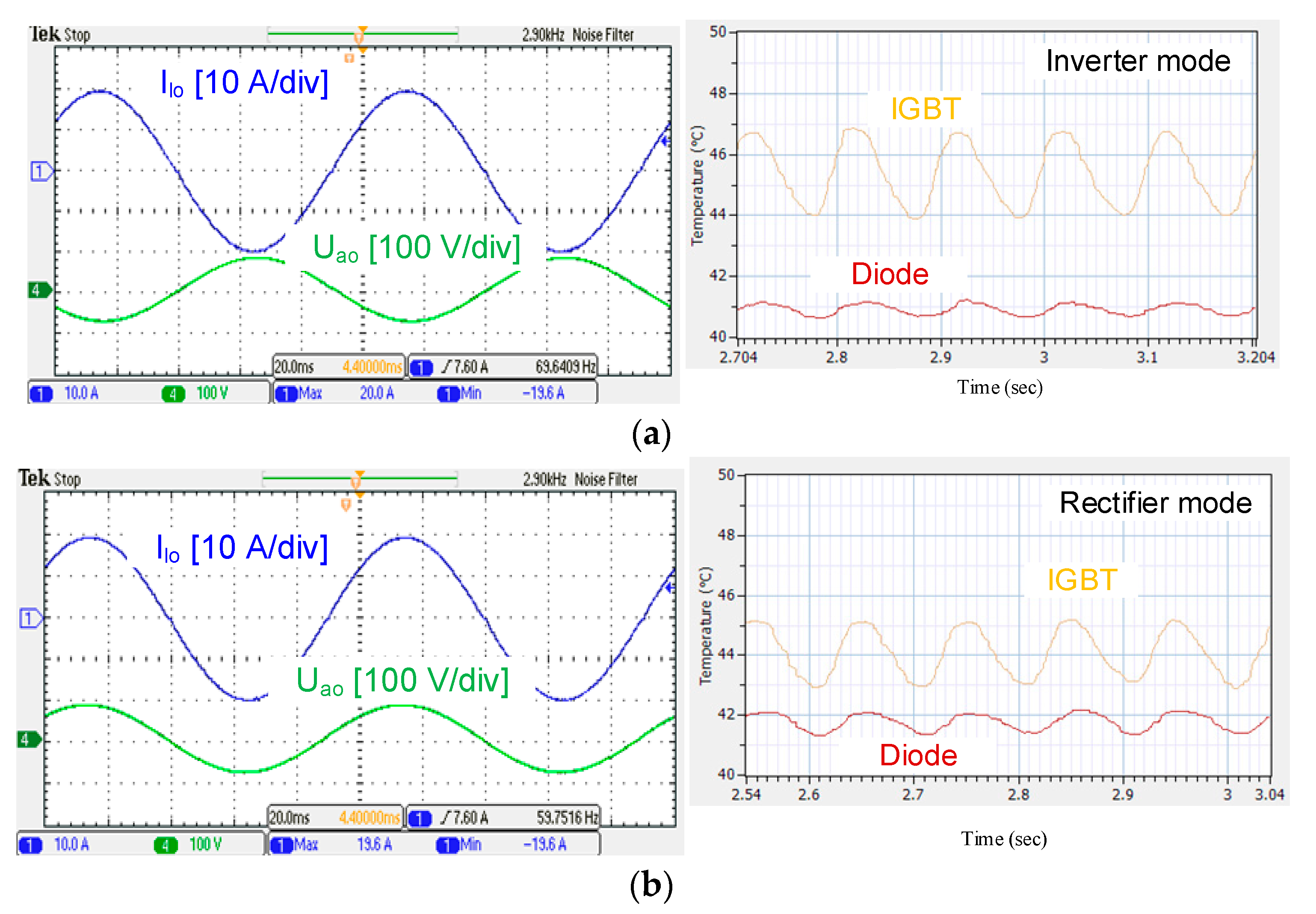
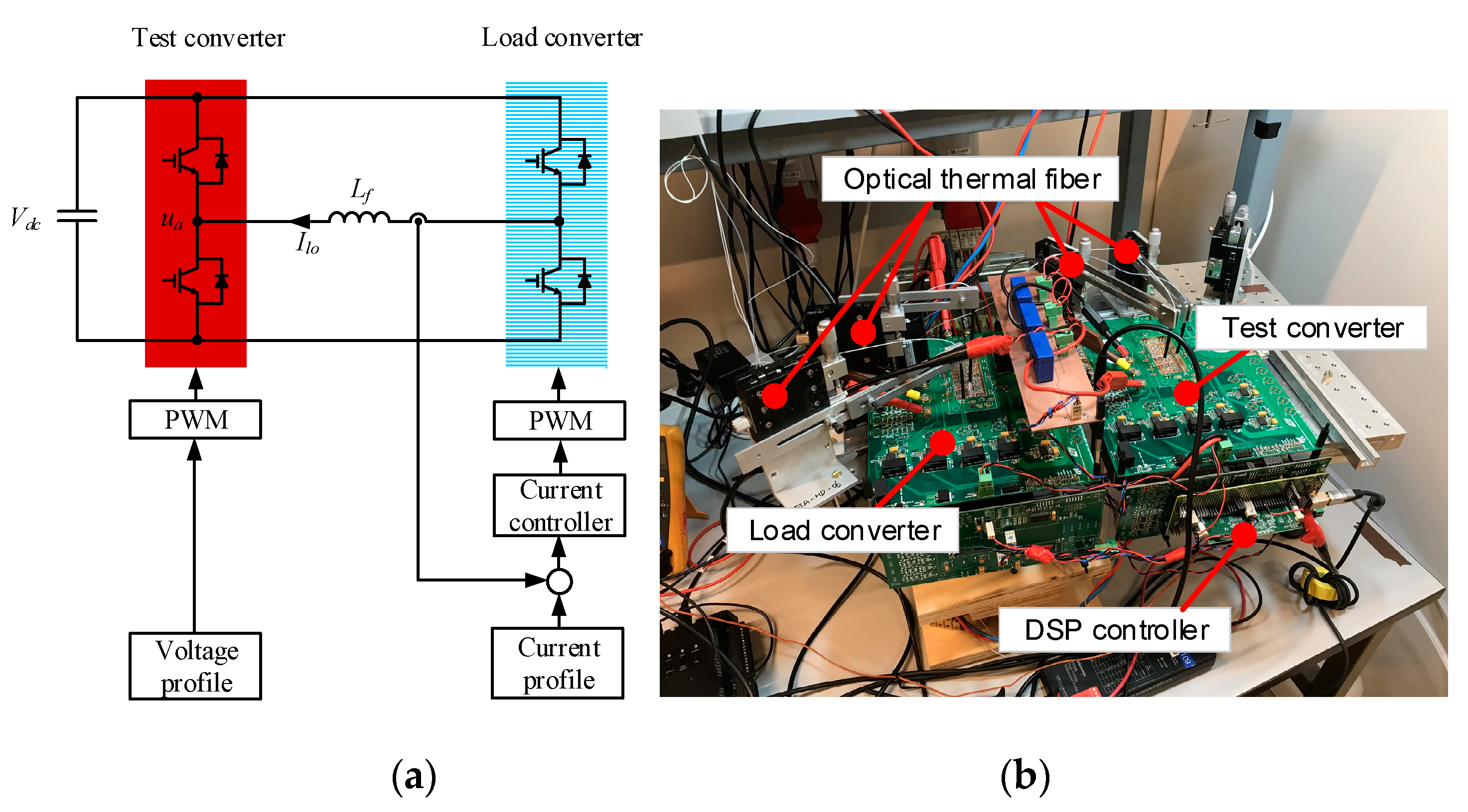
4.2. Simulation and Experimental Verification

Consistent with the converter parameters listed in Table 1, the simulation can be carried out by using PLECS (Piecewise Linear Electrical Circuit Simulation), a software tool for system-level simulations of electrical circuits developed by Plexim [24]. For the inverter and rectifier modes, the power loss and junction temperature of the IGBT and the diode are shown in Figure 9a,b, respectively. In the case of the inverter mode, the IGBT is the most stressed. It can be observed that the average loss dissipation consumes 20.7 W, and the junction temperature fluctuates between 53.8 and 67.7 °C. Nevertheless, the diode becomes the most stressed under the rectifier mode, with the average power loss of 12.3 W and the temperature swing of 10.5 °C.
In respect to the experimental setup, the control scheme of the test and load legs is shown in Figure 10a. By using the open-loop control, the driving signal of the test leg is generated from the required voltage profile. However, the driving signal of the load leg is produced by using a closed-loop control of the loading current. The photo of the experimental setup is shown in Figure 10b. It is worthwhile to mention that the control scheme is realized by means of a TI Digital Signal Processor (DSP) TMS320F28335 [25]. The loading current is measured by using the ADC module, while the PWM signals are generated by using ePWM module.
For the junction temperature measurement, the temperature swing is fluctuated within a fundamental period of 100 ms in this case study. The bandwidth of the temperature response needs to be fast, where the fiber-optical thermometer and thermographic camera are typical alternatives. In addition, both of them are capable to provide the electromagnetic isolation, which is preferred by the fast-switching transistors. To prepare the power modules for the thermographic camera, the dielectric gel needs to be removed, and then high-temperature material is painted across the chip surface in order to achieve the consistent emissivity. For the fiber-optical thermometer, the chip surface of the IGBT can be accessed without the removal of the dielectric gel, which reserves the function of the voltage isolation. Based on the temperature dependence of the band gap of the sensing material, a miniature spectrometer provides a spectrum with the position of the band edge, from which the temperature is calculated. A thermal fiber monitoring system from OpSens is applied, and the OTG-F sensor is selected due to the fastest response time of 5 ms [26].
As shown in Figure 11, the converter can be operated in either the inverter or rectifier mode. It is noted that the peak loading current is 20 A, the fundamental frequency is 10 Hz, and the switching frequency is 10 kHz. Besides, the heatsink temperature of the power module is controlled at 20 °C by using the refrigerated circulator, which indicates that the boundary condition of the experiment is exactly the same with the simulation. In the case of the inverter mode, the loading current is expected to be out of phase with the phase voltage. In respect of the junction temperature, it is noted that the temperature fluctuates with the fundamental frequency of 10 Hz. Moreover, the IGBT is more stressed compared to the diode. In the case of the rectifier mode, it is evident that the loading current is in phase with the phase voltage. Besides, the junction temperature of the diode is more stressed compared to the inverter mode, which is consistent with the analytical calculation. The detail thermal stress comparison between the simulation and experiment is listed in Table 3. It can be seen that, even though the inverter and rectifier modes can alter loss dissipation between the IGBT and the diode, the simulated thermal stress of both the IGBT and the diode is higher than in the experiment. This is because the loss curves of the power device are inherited from the datasheet, but are not accurately characterized by using the experimental setup. Moreover, the thermal impedance of the power module itself and cooling solutions also needs better characterization.

5. Conclusions

In this paper, a H-bridge platform is presented with the aim of emulating various loading conditions of a power converter (e.g., resistive, inductive and capacitive load). The basic operation principle and modulation scheme have been presented, both in the case of inverter and rectifier operations. Loss and thermal models of power semiconductors have been presented and discussed, including the key influential factors like power factor, loading current, fundamental frequency, and switching frequency. An experimental validation of the predicted losses is performed via measuring the semiconductors’ junction temperature via optical fibers. As an important outcome, loading conditions can be adjusted in order to obtain an arbitrary thermal stress. Furthermore, the test leg of the converter is able to operate with the desired power factor, operational frequency, and current loading. It can serve as an emulator to mimic the power converter oriented for the adjustable speed drive of machinery, grid-tied applications of PV/wind power inverter, etc.

Author Contributions

Conceptualization, D.Z. and F.I.; methodology, D.Z. and F.I.; validation, D.Z. and Y.P.; writing—original draft preparation, D.Z.; writing—review and editing, F.I., M.H., and F.B. All authors have read and agreed to the published version of the manuscript.

Funding

This research received no external funding.

Conflicts of Interest

The authors declare no conflict of interest.

References

  1. Blaabjerg, F.; Ma, K. Future on Power Electronics for Wind Turbine Systems. IEEE J. Emerg. Sel. Top. Power Electron. 2013, 1, 139–152. [Google Scholar] [CrossRef]
  2. Wang, H.; Liserre, M.; Blaabjerg, F.; Rimmen, P.D.P.; Jacobsen, J.B.; Kvisgaard, T.; Landkildehus, J. Transitioning to Physics-of-Failure as a Reliability Driver in Power Electronics. IEEE J. Emerg. Sel. Top. Power Electron. 2013, 2, 97–114. [Google Scholar] [CrossRef]
  3. Xiong, Y.; Cheng, X.; Shen, Z.; Mi, C.; Wu, H.; Garg, V. Prognostic and Warning System for Power-Electronic Modules in Electric, Hybrid Electric, and Fuel-Cell Vehicles. IEEE Trans. Ind. Electron. 2008, 55, 2268–2276. [Google Scholar] [CrossRef]
  4. Yang, S.; Bryant, A.T.; Mawby, P.A.; Xiang, D.; Ran, L.; Tavner, P. An industry based survey of reliability of power electronic converters. IEEE Trans. Ind. Appl. 2011, 47, 1441–1451. [Google Scholar] [CrossRef]
  5. Ji, B.; Song, X.; Sciberras, E.; Cao, W.; Hu, Y.; Pickert, V. Multi-objective design optimization of IGBT power modules considering power cycling and thermal cycling. IEEE Trans. Power Electron. 2015, 30, 2493–2504. [Google Scholar] [CrossRef] [Green Version]
  6. Gopireddy, L.R.; Tolbert, L.M.; Ozpineci, B. Power Cycle Testing of Power Switches: A Literature Survey. IEEE Trans. Power Electron. 2014, 30, 1. [Google Scholar] [CrossRef]
  7. Luo, H.; Iannuzzo, F.; Blaabjerg, F.; Turnaturi, M.; Mattiuzzo, E. Aging precursors and degradation effects of SiC-MOSFET modules under highly accelerated power cycling conditions. In Proceedings of the IEEE ECCE 2017, Cincinnati, OH, USA, 1–5 October 2017; pp. 2506–2511. [Google Scholar]
  8. Choi, U.-M.; Joergensen, S.; Blaabjerg, F. Advanced Accelerated Power Cycling Test for Reliability Investigation of Power Device Modules. IEEE Trans. Power Electron. 2016, 31, 8371–8386. [Google Scholar] [CrossRef]
  9. Czerny, B.; Lederer, M.; Nagl, B.; Trnka, A.; Khatibi, G.; Thoben, M. Thermo-mechanical analysis of bonding wires in IGBT modules under operating conditions. Microelectron. Reliab. 2012, 52, 2353–2357. [Google Scholar] [CrossRef]
  10. Wei, L.; Lukaszewski, R.; Lipo, T. Analysis of Power-Cycling Capability of IGBT Modules in a Conventional Matrix Converter. IEEE Trans. Ind. Appl. 2009, 45, 1443–1451. [Google Scholar]
  11. Oates, C. Accelerated life testing of a traction inverter. Power Eng. J. 1999, 13, 263–271. [Google Scholar] [CrossRef]
  12. Song, Y.; Cheng, R.; Ma, K. A Mission Profile Emulator for Permanent Magnet Synchronous Machine Drive System Based on Single-Phase H-Bridge Circuit. In Proceedings of the IEEE ECCE 2018, Portland, OR, USA, 23–27 September 2018; pp. 4972–4978. [Google Scholar]
  13. Ko, Y.; Andresen, M.; Buticchi, G.; Liserre, M. Thermally Compensated Discontinuous Modulation Strategy for Cascaded H-Bridge Converters. IEEE Trans. Power Electron. 2018, 33, 2704–2713. [Google Scholar] [CrossRef]
  14. Broeck, C.V.D.; Zeng, H.; Lorenz, R.D.; Doncker, R.W.D. A test bench for thermal characterization of IGBT power modules over mission profiles. In Proceedings of the PCIM Europe 2018, Nuremberg, Germany, 5–7 June 2018; pp. 1–8. [Google Scholar]
  15. Lai, W.; Chen, M.; Ran, L.; Alatise, O.; Xu, S.; Mawby, P. mLow dT stress cycle effect in IGBT power module die-attach lifetime modeling. IEEE Trans. Power Electron. 2018, 31, 6575–6585. [Google Scholar] [CrossRef]
  16. Hung, T.-Y.; Liao, L.-L.; Wang, C.C.; Chi, W.H.; Chiang, K.-N. Life Prediction of High-Cycle Fatigue in Aluminum Bonding Wires Under Power Cycling Test. IEEE Trans. Device Mater. Reliab. 2013, 14, 484–492. [Google Scholar] [CrossRef]
  17. Ghirmire, P.; Beczkowski, S.; Munk-Neilson, S.; Rannestad, B.; Thogersen, P.B. A review on real time physical measurement techniques and their attempt to predict wear-out status of IGBT. In Proceedings of the EPE 2013, Lille, France, 2–6 September 2013; pp. 1–10. [Google Scholar]
  18. Zhou, D.; Song, Y.; Blaabjerg, F. Thermal stress mapping of power semiconductors in H-bridge test bench. In Proceedings of the IEEE CPE-PWERENG 2019, Sonderborg, Denmark, 23–25 April 2019; pp. 1–6. [Google Scholar]
  19. Wintrich, A.; Ulrich, N.; Werner, T.; Reimann, T. Application Manual Power Semiconductors; Semikron: Nuremberg, Germany, 2015. [Google Scholar]
  20. Backlund, B.; Schnell, R.; Schlapbach, U.; Fischer, R.; Tsyplakov, E. Applying IGBTs; ABB. Semiconductors: Lenzburg, Switzerland, 2007. [Google Scholar]
  21. Zhou, D.; Blaabjerg, F.; Gae, F.B. Optimized Demagnetizing Control of DFIG Power Converter for Reduced Thermal Stress during Symmetrical Grid Fault. IEEE Trans. Power Electron. 2018, 33, 10326–10340. [Google Scholar] [CrossRef]
  22. Zhou, D.; Blaabjerg, F.; Lau, M.; Tonnes, M. Optimized Reactive Power Flow of DFIG Power Converters for Better Reliability Performance Considering Grid Codes. IEEE Trans. Ind. Electron. 2014, 62, 1552–1562. [Google Scholar] [CrossRef]
  23. Infineon IGBT Power Module FP50R12KT4. Available online: https://www.infineon.com/cms/en/product/power/igbt/igbt-modules/fp50r12kt4/ (accessed on 1 April 2020).
  24. PLECS User Manual. Available online: https://www.plexim.com/sites/default/files/plecsmanual.pdf/ (accessed on 1 April 2020).
  25. TI Application Note, TMS320F2833x Digital Signal Controllers. Available online: http://www.ti.com/lit/ds/symlink/tms320f28335.pdf/ (accessed on 1 April 2020).
  26. OTG-F Fiber Optic Temperature Sensor. Available online: https://opsens-solutions.com/products/fiber-optic-temperature-sensors/otg-f// (accessed on 1 April 2020).
Figure 1. Configuration of H-bridge circuit and phasor diagram between test leg and load leg. (a) Single-phase H-bridge circuit. (b) Phasor diagram in the case of inverter mode. (c) Phasor diagram in the case of rectifier mode.
Applsci 10 04340 g001
Figure 2. Activated power switches at various operation modes. (a) Inverter mode. (b) Rectifier mode.
Applsci 10 04340 g002
Figure 3. Schematic waveforms of the loss calculation under the steady-state operation. (Note: Tf denotes the fundamental period, and Tsw denotes the switching period.).
Applsci 10 04340 g003
Figure 4. Thermal model of power semiconductor for thermal cycling caused by the fundamental frequency.
Applsci 10 04340 g004
Figure 5. Impacts of various power factors (PFs) on power module. (a) Loss dissipation. (b) Mean junction temperature. (c) Junction temperature swing.
Applsci 10 04340 g005
Figure 6. Impact of various loading currents (Ilo) on power module. (a) Loss dissipation. (b) Mean junction temperature. (c) Junction temperature swing.
Applsci 10 04340 g006
Figure 7. Impact of various fundamental frequencies (f1) on power module. (a) Loss dissipation. (b) Mean junction temperature. (c) Junction temperature swing.
Applsci 10 04340 g007
Figure 8. Impacts of various switching frequencies (fsw) on power module. (a) Loss dissipation. (b) Mean junction temperature. (c) Junction temperature swing.
Applsci 10 04340 g008
Figure 9. Loss dissipation and junction temperature of IGBT and diode with fundamental frequency of 10 Hz and switching frequency of 10 kHz. (a) Inverter mode. (b) Rectifier mode.
Applsci 10 04340 g009
Figure 10. Experimental setup of H-bridge circuit. (a) Control block diagram. (b) Photo of experimental setup.
Applsci 10 04340 g010
Figure 11. Experimental results in terms of the loading current and junction temperature of power semiconductors. (a) Inverter mode. (b) Rectifier mode.
Applsci 10 04340 g011
Table 1. Parameters and Rated Condition of Converter.
Rating of Power Device1200 V/50 A
Filter inductor Lf300 μH
DC-link voltage Vdc400 V
Rated power factor PF−1
Rated peak current Ilo20 A
Rated fundamental frequency f110 Hz
Rated switching frequency fsw10 kHz
Table 2. Parameters Used in Loss Model and Thermal Model of Power Semiconductors [23].
IGBTDiode
Loss modelVCE @ 50 A, Tj = 150 °C (V)2.25/
VF @ 50 A, Tj = 150 °C (V)/1.65
Eon @ 50 A, Tj = 150 °C (mJ)7.7/
Eoff @ 50 A, Tj = 150 °C (mJ)4.8/
Err @ 50 A, Tj = 150 °C (mJ)/3.7
Thermal modelFourth order thermal resistance Rth (°C/kW)0.03240.0486
0.17820.2673
0.17280.2592
0.15660.2349
Fourth order thermal time constant τth (s)0.010.01
0.020.02
0.050.05
0.10.1
Table 3. Thermal Stress Comparison between Simulation (Sim.) and Experiment (Exp.).
IGBTDiode
Sim.Exp.ErrorSim.Exp.Error
Inverter modeJunction temperature swing (°C)53.8~67.743.9~46.9/50.1~56.140.8~41.3/
Mean temperature (°C)60.845.415.453.141.112.0
Temperature deviation (°C)13.93.010.96.00.55.5
Rectifier modeJunction temperature swing (°C)52.2~60.242.8~45.2/53.0~63.541.2~42.2/
Mean temperature (°C)57.244.013.258.341.716.6
Temperature deviation (°C)10.02.47.610.51.09.5

