Abstract
Carbon nanotube/silicon (CNT/Si) heterojunction solar cells represent one new architecture for photovoltaic devices. The addition of MoS2 to the devices is shown to increase the efficiency of the devices. Two structures are explored. In one case, the single wall carbon nanotubes (SWCNTs) and MoS2 flakes are mixed to make a hybrid, which is then used to make a film, while in the other case, a two layer system is used with the MoS2 deposited first followed by the SWCNTs. In all cases, the solar cell efficiency is improved largely due to significant increases in the fill factor. The rise in fill factor is due to the semiconducting nature of the MoS2, which helps with the separation of charge carriers.
1. Introduction
It is clear that the sun can provide more energy than the current global daily energy consumption as well as fulfill future requirements for many years. Solar power is the most sustainable renewable energy and will help lower greenhouse gas emissions. Additionally, utilising the sun in a distributed network can eliminate energy lost due to the distribution grid, which accounts for almost 25% of produced electricity being lost [1].
The search for novel solar cell designs as an alternative to standard silicon solar cells is important for the future of renewable energy production. One such alternative design is the carbon nanotube/silicon (CNT/Si) heterojunction solar cell. The first such cells were designed by Wei et al. in 2007 [2,3] using double wall carbon nanotubes (DWCNTs) deposited via water expansion and aqueous film transfer of an as-grown chemical vapour deposition (CVD) film. While these cells only had a photoconversion efficiency of 1.3% (compared to commercial cells at 20%–30%), many improvements have since been made to the cell design and doping methods, with 15% efficiencies reported in 2012 [4] and 17% efficiencies reported in 2015 [5].
The typical architecture for these cells is much like that of a single-junction n-type crystalline silicon solar cell with a front side emitter layer replaced by a film of p-doped CNTs [2]. While the initial design used DWCNTs, most designs use single wall carbon nanotube (SWCNT) electrodes; however, multiwall carbon nanotubes (MWCNTs) may also be used [6,7]. Jia et al. [8] performed the first comparison between SWCNTs, DWCNTs, and MWCNTs for use in CNT/Si cells in terms of the area density of the films. The majority of research performed on nanotube/silicon cells uses a mixture of nanotube types to form the film as nanotubes are grown as a mixture of types. Tune et al. investigated the effects of fabricating cells with pure metallic or semiconducting nanotubes versus cells with an as-grown mix of types [9]. Similar experiments have been undertaken by Harris et al. in their comparison of semiconducting and metallic nanotube films on silicon [10]. Overall, the metallicity of the nanotube film plays a significant role in the cell operation. In all cases, the CNT film acts as a component of the heterojunction setting up a built-in potential to enable charge separation, as a highly conductive network for charge collection and transport, and as a transparent electrode to allow good light illumination of, and photocurrent generation in, the silicon base [7].
A variety of approaches have been examined to improve device performance. For example, in 2008, Li et al. [11] found that treatment of the SWCNT layer with the p-dopant thionyl chloride (SOCl2) increased the power conversion efficiency of the cells by over 45% (relative) by lowering the sheet resistance and increasing the short-circuit current density and open-circuit voltage. Jia et al. experimented with doping the nanotube film using nitric acid [12]. Doping using CuCl2/Cu(OH)2 colloidal ethanol solution looks to be a particularly promising approach and demonstrates considerable stability compared to many of the other approaches [13]. Other p-dopants can be used in the treatment of SWCNT films in order to increase the efficiency of the CNT/Si heterojunction cell, including gold chloride (AuCl3) [14].
Research was carried out by Tune et al. [15] in 2013 to find an optimal thickness for a film using large diameter arc-discharge SWCNTs with high carboxyl functionality. They determined that a film transmittance of 70% gave an optimal efficiency, although thicker films displayed fairly stable efficiencies. The device efficiency was found to taper significantly with thinner films. This was due to a decrease in the amount of SWCNT/Si contacts for charge separation and an exponential increase in sheet resistance as the film conductivity became dominated by the limited pathways in the very thin SWCNT films. One limiting factor in the performance of the CNT/Si heterojunctions is the film morphology. Highly ordered, aligned carbon nanotube films have been produced using various techniques [16,17,18,19,20]. The ordered alignment of the SWCNTs allows a thin, highly transparent, very smooth film to be produced, which does not suffer from the drawbacks of thin films produced via other methods (such as poor contact with the silicon substrate and a poorly formed nanotube network with many electronic charge traps and physical holes in the film).
Front-side reflectance detracts significantly from the photocurrent production of photovoltaic devices. Random pyramids in the CNT/Si heterojunction design improve the efficiency [21,22,23], as observed in other photovoltaic devices [24], while the use of silicon nanowires has also been investigated by Petterson et al. The nanowires dramatically lowered the surface reflectance leading to improved performance [25]. Another approach to reduce the silicon reflectance involved spin coating of a TiO2 colloid giving a nanoparticulate layer of 50–80 nm in thickness on the surface [26]. In the case of the nanotube/silicon cells, the layer subdued the light reflection significantly to give cell efficiencies above 15% [4]. Recently, Wang et al. investigated the application of molybdenum oxide (MoOx) and zinc oxide (ZnO) as cheap, environmentally friendly antireflection layers [5]. Polymers such as poly(dmiethylsiloxane) (PDMS), [27] polystyrene (PS), [27] poly(methylmethacrylate) (PMMA) [27,28], or NOA63 [29] have also been examined for their antireflective properties and have the added bonus of providing protection from the environment for added stability in addition to the improved performance.
Other work to improve the performance of nanotube/silicon cells has involved putting a layer between the SWCNTs and the silicon. For example, Tune et al. reported a cell design combining a first layer of polyaniline (PANI) and then a second layer of SWCNTs on an n-silicon substrate. The SWCNT/PANI/Si junctions showed a maximum efficiency of 9.7% [30]. The use of other hole transporting materials such as (3,4-ethylene dioxythiophene):poly(styrenesulfonate) (PEDOT:PSS), [31] 2,2′,7,7′-tetrakis(N,N’-di-p-methoxyphenylamine)-9,9′-spirobifluorene (spiro-OMeTAD), [32] 4,4′-(naphthalene-2,6-diyl)bis(N,N-bis(4-methoxyphenyl)aniline) (NAP), and (E)-4′,4′’’-(ethene-1,2-diyl)bis(N,N-bis(4-methoxyphenyl)-[1′’,1′’’-biphenyl]-4amine) (BPV) [33] have also been reported.
There has been huge interest in developing solar cells using 2D materials. For instance, molybdenum disulfide (MoS2) has distinctive optical, photodetection, and electronic characteristics [34]. In this research project, using molybdenum disulfide films, SWCNT suspensions, and hybridised MoS2 with SWCNTs, the objective was to fabricate solar cells where the n-type semiconductor is the n-type silicon and the p-type semiconductor is the SWCNTs (Figure 1i). Then the molybdenum disulfide was added as an n-type semiconductor to the SWCNT/Si based solar cells to improve the devices’ efficiency. The MoS2 was used to make hybrids of SWCNTs/MoS2 by filtering different volumes of MoS2 and SWCNTs at the same time and then attaching this mixed film to the n-type Si (Figure 1ii). Alternatively, a layered SWCNTs/MoS2/n-type Si solar cell was built where first the MoS2 film is attached to the Si substrate and then a SWCNT film is attached over the MoS2 film (see Figure 1iii). Ultimately this means three types of devices will be compared where the films placed over the Si substrate are changing: (1) SWCNT only, (2) hybrid of SWCNT/MoS2, and (3) a layer of MoS2 followed by a layer of SWCNTs. Previous work has produced the Si/MoS2/SWCNT layered structure (see Figure 1iii) [35]. Other work using 2D materials has often made hybrids of the 2D materials and the SWCNTs [36,37]. This work presents the first direct comparison between these two approaches using the same dispersions of materials to probe if one approach will provide better performance compared to the other.
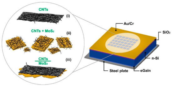
Figure 1.
Structures of devices made in this work. All devices involve putting a thin films of various materials on the silicon. (i) single wall carbon nanotubes (SWCNTs) only; (ii) SWCNT + MoS2 hybrids; and (iii) a layer of MoS2 with a SWCNT layer placed on top.
2. Materials and Methods
2.1. Preparation of Stock Dispersions
Few layer molybdenum disulfide colloidal suspensions were obtained from FlexeGRAPH. The SWCNT suspension was prepared as reported previously [15]. In brief, 0.5 mL of Triton X-100 (SIGMA ALDRICH, Castle Hill, NSW, Australia) mixed with 49.5 mL Milli-Q water (50 mL, 1% v/v). The suspension was bath sonicated for 20 min and 0.005 g of large diameter arc-discharged, P3-SWCNTs (Carbon Solutions, Inc. Columbia, CA, USA) were added and the dispersion bath was sonicated for 1 h. After centrifugation for 1 h, the supernatant was collected, then recentrifuged for an additional hour and finally collected and used.
SWCNTs/MoS2 hybrid suspensions were prepared by keeping the SWCNTs dispersion at the same volume (300 µL) and changing the MoS2 dispersion volume (100–1000 µL and 2 mL).
2.2. Preparation of Electrodes
The preparation of the films for both characterisation and solar cell production was done using vacuum filtration as described previously [15]. Briefly, vacuum filtration was used with two types of membranes: A mixed cellulose ester membrane (MCE) with small nano-sized pores (TYPE VSWP 0.025 μm, Millipore “stencil”) and over it another filter paper with large nano-sized pores that had four holes (TYPE HAWP 0.45 μm, Millipore “target”) to give four identical films in one filtration. The required volume of the suspension was diluted with 250 mL of Milli-Q water, filtered with the two membranes, which had differences in the flow rates (between the target and stencil membranes). This produced precise film thicknesses and optical densities by changing the volume of the suspensions used as well as well-defined film shapes with identical characteristics on the target membrane. The filtered film was washed carefully (using three washes of 50 mL deionised water).
2.3. Preparation of Si Substrates
For device preparation, the silicon n-type substrate (CZ, 5–25 Ω.cm, <100> 100 mm diameter single-SSP, ABC GmbH with thermal oxide with 100 nm side polished, thickness 525 ± 25 μm, n/phosphorous-doped and SiOx layer, München) was cleaned with piranha for 10 min, rinsed with Milli-Q water, then bath sonicated in acetone for 10 min and dried with N2.
To make the blank device substrates, a thin layer of the photoresist (AZ 1518) was placed onto the silicon and spun using the spin coater for 30 s. The photoresist was soft baked using a hot plate (100 °C) for 1 min and cooled down to room temperature. UV light exposure for 30 s printed the mask pattern over the Si substrate. The substrate was immersed in the developer solution (AZ 326 MIF) for 1 min, rinsed with Milli-Q water and dried with N2. The patterned wafer was then coated with 5 nm of Cr and then with 145 nm of Au using a Q300T-D Dual Target Sputter Coater to form the top contact for the substrates. The Si substrate was immersed in acetone for 30 min to remove the photoresist leaving a circular active area of 0.08 cm2.
Before adding the SWCNT or MoS2 or SWCNT/MoS2 hybrid film, a buffered oxide etch (BOE) treatment was done by applying one drop of 6:1 ammonium fluoride: hydrofluoric acid over the circular active area for approximately 2 min. The silicon substrate was then rinsed with deionised water and ethanol and dried with N2.
2.4. Preparation of Solar Cells
For all prepared films, they were transferred to glass or bare Si for characterisation or to patterned Si substrates for device preparation. Where Si was used for characterisation, the initial cleaning was undertaken by bath sonication at the room temperature in acetone for 10 min (rinsed with Milli-Q water, ethanol and dried with N2). For the transfer, a circular region (0.32 cm2) of the membrane with the film on it was cut out of the filtered area and wetted with Milli-Q water. A piece of Teflon was placed over the film, followed by a piece of glass to form a glass/substrate/SWCNT film/Teflon/glass sandwich. The Teflon was used to avoid the risk of the MCE/nanotube film attaching to the upper layer of glass rather than the substrate. Subsequently, the sandwich was heated at 80 °C for 15 min and then cooled down at the room temperature for 1 h. The substrate with the film/membrane now attached was immersed in acetone for 30 min to dissolve the membrane to yield the sample or device.
The back contact of the final device was formed on the reverse side of the substrate by scratching with a diamond-tipped pen to access the silicon underneath the 100 nm silicon oxide layer. A small amount of gallium-indium eutectic (eGaIn, SIGMA ALDRICH, Castle Hill, NSW, Australia) was then applied to the scratched area and a roughly 2 cm by 2 cm square piece of stainless steel was attached to the silicon. This device was called the “as prepared” solar cell.
2.5. Post Treatments
The solar cells were taken through a series of chemical treatments. The first treatment was with 2% hydrofluoric acid (HF) by dropping one drop of 2% HF over the active area for 15 s followed by rinsing with Milli-Q water, ethanol and drying with N2. The second treatment was a thionyl chloride (SOCl2) treatment completed by applying one drop over the film to make the SWCNTs more conductive. The sample was left in air to dry, then rinsed with ethanol and N2 to dry. The third treatment was the 2% HF again by the same manner to remove any oxidisation from the thionyl chloride step. After each treatment the efficiency was tested and measurement after the final treatment are the final efficiencies reported. For any SWCNTs on glass, similar treatments were applied but 2% HCl was used instead of 2% HF to avoid etching of the glass substrate.
2.6. Characterisation
The efficiency of the solar cells examined using an Oreil solar simulator, and the solar device data was processed using a custom program written in LabView, connected to a Keithley data acquisition unit (Keithley 2400 source), which calculated the vital parameters from the JV curve, both under illumination and in the dark.
Atomic Force and Scanning Electron Microscopy (AFM and SEM)
The MoS2, SWCNTs, and hybrid MoS2/SWCNTs films made with different suspension volumes were mounted on silicon substrates and examined using a Bruker Multimode 8 AFM with Nanoscope V controller operating in tapping mode. An Inspect FEI F50 SEM was used for the electron microscopy.
3. Results
3.1. Characterisation
AFM scans were used to prove the presence of the chemically exfoliated MoS2 flakes. Figure 2a shows a high resolution image of a single MoS2 flake while Figure 2b shows a lower resolution SEM image of an MoS2 sample showing the range of flake sizes in the dispersion (in both lateral size and thickness). The range of flake sizes may be helpful to create a rougher surface that will reduce the light reflection thus enhance light absorption and overall cell performance [38]. The thickness of the flake in Figure 1a was measured to be ~5 nm. Given that monolayers of MoS2 are about 1 nm thick, it is clear that the flakes in our dispersions are several layers thick [39,40]. There are a broad range of lateral sizes for the flakes but they are in the range reported by others. The images with the SWCNTs show the typical morphology of the films with the ridges observed thought to be slight variations in the flows through different parts of the filtration membranes.
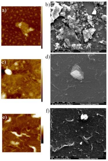
Figure 2.
(a) AFM image of typical MoS2 flake; image size is 855 nm × 855 nm with a z-range of 24 nm. (b) Wide view SEM image of MoS2 flakes in the dispersion. (c) AFM of SWCNT/MoS2 hybrid made by mixing 600 µL of MoS2 dispersion with 300 µL SWCNT dispersion; image size is 2.0 µm × 2.0 µm with a z-range of 220 nm. (d) SEM image of SWCNT/MoS2 hybrid made by mixing 600 µL of MoS2 dispersion with 300 µL SWCNT dispersion. (e) AFM of SWCNT/MoS2 layered system made by first depositing a film made from a 600 µL of MoS2 dispersion followed by a film made using 300 µL SWCNT dispersion; image size is 6.0 µm × 6.0 µm with a z-range of 800 nm. (f) SEM image of SWCNT/MoS2 layered system made by first depositing a film made from a 600 µL of MoS2 dispersion followed by a film made using 300 µL SWCNT dispersion.
3.2. Properties of the Reference Cell
A standard cell was made with just SWCNTs in the top layer. The detail characteristics of this cell are provided in the supplemental material. The average efficiency of this cell was 6.83% and other cells made using MoS2 will be compared to this value. Figure S1 shows the transmittance of the SWCNT film while Figures S2 and S3 provide the dark and light JV curves respectively and the effects of the various treatments on the device performance, which are consistent with those reported previously [15]. Table S1 gives the detailed parameters for the reference cells.
3.3. Optimisation of the Electrode Transparency
Previous work to find an optimal thickness for a SWCNT film determined that a film transmittance of ~70% gave an optimal efficiency, although thicker films displayed fairly stable efficiencies. The device efficiency was found to taper significantly with thinner films. This was due to a decrease in the number of intimate SWCNT/Si contacts for charge separation and an exponential increase in sheet resistance as the film conductivity became dominated by the limited pathways in very thin films [15]. To determine the best transparency for the systems using MoS2, cells were made maintaining the volume ratio between the SWCNT and MoS2 dispersions and increasing the total volume used thereby increasing the film thickness. The summary of the results are shown in Figure 3 while the detailed parameters are provided in Table S2 from the representative JV curves given in Figure S4.
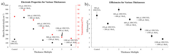
Figure 3.
(a) Electrode properties for films of different thicknesses; (b) Efficiencies of solar cells with different thickness films.
As expected, the transmission decreases as the amount of material used to create the film is increased. The same trends observed for SWCNTs films are found for the SWCNT/MoS2 hybrid films. For the films with approximately the same transmission (300 µL of SWCNT and 300 µL of SWCNT + 400 µL of MoS2), the addition of the MoS2 does improve the solar cell performance. Determining the best ratio of the dispersion will improve this performance further. The relatively poor performance of thinnest films can be traced to the low fill factor. This arises due to the lack of connectedness of the conducting layer, which will lead to a higher level of recombination. The decrease in performance of cells with thicker layers is due to lower short circuit currents as a result of the lower transmittance of the films. The darker layers mean less light makes it through to the silicon substrate and hence fewer excitons are created.
3.4. Optimisation of the Oxide Layer Thickness
The thickness of the oxide layer on the silicon is also important to achieve the best efficiency. The exact thickness required is still a matter of some debate [41,42,43]. The second HF etch in the treatment series is used to control the oxide thickness in the final cells tested. In the normal procedure, the etch is carried out for 15 s. Further investigations were undertaken using etching for 30, 45, and 60 s. The comparison of the performance for these different cells is provided in the supplemental information in Table S3 and Figure S5. In all cases of extra etching, the overall performance is poorer. This is likely due to the lack of an oxide layer. A thin oxide layer was found to suppress dark saturation current, inhibit recombination, and lead to an increase in minority carrier lifetime and open circuit voltage (Voc) [42]. The passage of majority carriers across the junction is suppressed by the oxide, whereas the tunnelling-based passage of minority carriers is unaffected. The extra etching time leads to little change in Voc until 60 s where the Voc drops significant probably due to the complete removal of the oxide. For all other data presented, a 15 s etch will be used.
3.5. Optimisation of the Component Ratio
A set of devices was made to determine the best ratio SWCNT to MoS2 dispersion. The summary of the results are shown in Figure 4 while the detailed parameters are provided in Table S4 from the representative JV curves given in Figure S6.
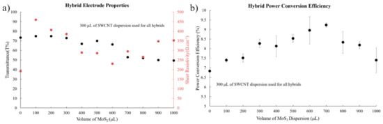
Figure 4.
(a) Electrode properties for films of different ratios of SWCNT and MoS2 dispersions; (b) Efficiencies of solar cells with films made with different ratios of SWCNT and MoS2 dispersions.
The optical properties of the films (transmittance) did not change greatly up to half mL of MoS2. This is due to the low concentration of the MoS2 dispersion. At the same time, the sheet resistance of the films decreased as adding the extra material to the film helps to bridge any gaps in the SWCNT connections and helps to lower the resistance. Figure 2c,d clearly shows the SWCNTs wrapped around the MoS2 flakes and this will help improve conductivity.
The overall trend in the solar cell behaviour is provided in Figure 4b. The addition of any amount of MoS2 improves the performance of the cells with a maximum average efficiency observed of 9.23% for the addition of 700 µL of MoS2 dispersion to 300 µL of SWCNT dispersion. Jsc changes very little over all the cells. Given the small changes in transmittance, this is not unexpected. The largest changes are in fill factor and Voc. The fill factor increases from 0.53 for the SWCNT only film up to values on the order of 0.7. Adding the extra semiconducting element in the film will provide a pathway for one type of charge carrier. SWCNTs are amipolar and hence can carry both types of charge carriers, which provides opportunities for recombination and hence lower fill factors. The MoS2 flakes provide a pathway to remove the holes from the nanotubes and hence lower the recombination rate. The increased lifetime of the holes will lead to improved fill factors as observed.
The increase in Voc observed is slightly more varied but always higher than the SWCNTs only. This indicates that the two materials interact to shift energy levels involved in the transitions central to the operation of the devices. The variability will stem from the random dispersion of the flakes through the SWCNT film. The drop in efficiency for high MoS2 loadings is due to the slight decreases in transmittance, which lowers the observed Jsc.
3.6. Layered Structure
A final set of cells was made by first putting a MoS2 layer on the Si and then placing a SWCNT layer over the top of the MoS2 layer. The SWCNT electrode was made using 300 µL of the SWCNT dispersion for all cells to keep the thickness of the SWCNT layer constant. The summary of the results are shown in Figure 5 while the detailed parameters are provided in Table S5 from the representative JV curves given in Figure S7. The cell with only a layer of MoS2 flakes gave no current. This suggests the MoS2 is n-type, [38] the same as the Si, and hence no heterojunction was created meaning there is no ability to separate charges.
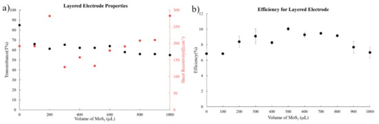
Figure 5.
(a) Electrode properties for films made with a layer of MoS2 covered by a film of SWCNTs; (b) Efficiencies of solar cells with films made with a layer of MoS2 covered by a film of SWCNTs.
The observations are very similar to the hybrid system where there is little change in Jsc but fill factor and open circuit voltage are enhanced. Average cell efficiencies of 10.04% are observed for devices made using 500 µL of MoS2 dispersion to form the first layer. The small changes in transmittance are consistent with the constant Jsc. In this case, the presence of an n-type layer on the Si will help the transfer of holes to the SWCNT layer, which will improve the fill factor and hence efficiency. Similar enhanced hole transport has been reported in a graphene/MoS2/Si system [44] where the energy levels due to the insertion of the MoS2 also lead to effective electron blocking by the MoS2 layer. For the SWCNT system, the observed Voc does shift from 0.515 V for SWCNTs only to 0.575 V for the system with the MoS2 layered under the SWCNTs, which is similar to the increases observed for the graphene system suggesting the MoS2 will also play a role in blocking electrons. The decrease in efficiency at higher loadings in this case will be due to the fact that thicker coverages of MoS2 will be pushing the SWCNTs further from the Si and hence the quality of the heterojunction that is established will be decreasing. It is possible that junctions between the MoS2 and SWCNTs could be established but these will be much smaller in area than the junction made with the substrate.
The results clearly show that the layered system performs better than the hybrid system. The efficiencies reported in this work are among the highest reported for systems using 2D materials (shown in Table 1). Our previous work using the layered MoS2 system [35] reported slightly higher efficiencies, which may be due to some degradation of the MoS2 dispersion. The better performance of the layered system points to the fact that modification at the interface of the heterojunction is more effective at improving performance than addition of material within the film. Given that photon absorption occurs in the Si substrate, the importance of transferring the charge carriers across the heterojunction is paramount to performance. The MoS2 layer assists this transfer across the junction. The higher performance of the layered system means that the facilitated charge transfer is more effective at improving efficiencies than the additional material in the SWCNT films (hybrid system) even though this extra material in the film will help charge carrier lifetime. Additionally, of course, in the hybrid the distribution of the 2D material is completely random and hence there is no guarantee that all the material will be used effectively to help performance.

Table 1.
Device efficiencies for various carbon nanotube/silicon (CNT/Si) devices produced using 2D materials.
The results in this current paper are similar to those reported by Cao’s group using grapheme [45]. In this case, the graphene between the SWCNTs and the Si provided a dramatic increase in efficiency from 1.4% to 8.00%. With the addition of the antireflection layers and doping of the SWCNTs, impressive efficiencies of 14.9% are obtained. It would be expected that the higher conductivity of the graphene might help the charge transfer and, while it is true that a larger improvement is observed in the graphene, the ultimate performance is less than the MoS2 case. This indicates that the semiconducting nature of the MoS2 does help reinforce the required charge separation. Cao’s work also put the graphene on top of the SWCNTs and this system also showed improved performance likely due to improved conductivity; however, the efficiencies were only half those observed with the graphene between the SWCNTs and the Si.
Figure S8 and Table S6 provide the parameters for the best performing cells of each type. The layered structure gave the best results. This is due to the fact that the MoS2 layer is in effect acting like a hole transport layer helping the transfer of charge carriers created in the Si substrate to the SWCNT layer where they can be transported to the electrode. This will help to minimise the number of electrons that enter the SWCNT layer thus minimising the possibility of recombination. Table 1 provides a summary of the work done to include 2D materials in the SWCNT/Si system [47] showing that the efficiencies reported in this work are among the best reported. All the work together supports the fact that a layered approach will give the best performance.
4. Conclusions
The addition of MoS2 flakes was shown to improve the performance of SWCNT/Si heterojunction solar cells. Cells with two different structures were explored; namely cells where the SWCNTs and MoS2 flakes were mixed together in one layer or cells where the MOS2 layers was deposited first followed by the SWCNT layer. The cells with a MoS2 layer covered by the SWCNTs gave the best performance. The improvement is significant with increases in efficiencies from 6.83% to 10.04% observed. The increase in device efficiency can be largely attributed to significant increases in fill factor, which are caused by the hole transport capabilities of the n-type MoS2 flakes. The fact that the layered systems give the highest performance highlights that tuning of the interface between the materials in the device is the most effective way to enhance efficiency.
Supplementary Materials
The following are available online at https://www.mdpi.com/2076-3417/10/1/287/s1. Figure S1: The absorption spectrum for the 300 μL SWCNTs-dispersion. Figure S2: Dark curves for the SWCNTs-n-Silicon based solar cell at different stages of treatment made using 300 μL of the SWCNT dispersions. Figure S3: Light curves for the SWCNTs-n-Silicon based solar cell at different stages of treatment made using 300 μL of the SWCNT dispersions. Table S1: The cell parameters for the reference SWCNTs-n-Si solar cell made with 300 μL of SWCNT dispersion. Figure S4: Light curves for the cells made with MoS2/SWCNT hybrid films of various thicknesses. Table S2: The cell parameters for devices made with MoS2/SWCNT hybrid films of various thicknesses. Figure S5: Light curves for the SWCNTs-n-Silicon reference solar cell and cells made with MoS2/SWCNT hybrids after various HF etching times. Table S3: Parameters for the reference SWCNTs-n-Si solar cell made with 300 μL SWCNT dispersion and cells made with MoS2/SWCNT hybrids after various HF etching times. Figure S6: Light curves for the SWCNTs-n-Silicon reference solar cell and cells made with MoS2/SWCNT hybrids using various ratios of dispersions. Table S4: The cell parameters for the reference SWCNTs-n-Si solar cell and cells made with MoS2/SWCNT hybrids using various ratios of dispersions. Figure S7: Light curves for the cells made with a layer structure with the Si first covered a MoS2 layer, which is then covered by a SWCNT layer. Table S5: The parameters for cells made with a layer structure with the Si first covered a MoS2 layer, which is then covered by a SWCNT layer. Figure S8: Representative light curves for the best average cells. Table S6: The parameters for the best average cells.
Author Contributions
S.A., L.Y., A.S.R.B. and T.G. carried out the investigations and undertook the data analysis. J.G.S. conceptualised and supervised the project as was also responsible for funding acquisition. S.A. and J.G.S. were responsible for the writing—original draft preparation while all authors were involved in writing—review and editing. All authors have read and agreed to the published version of the manuscript.
Funding
This research was funded by the AUSTRALIAN RESEARCH COUNCIL, grant number DP150101354 and DP160101301.
Acknowledgments
S.A. and A.S.R.B. acknowledges Saudi Arabian Cultural Mission (SACM) and the Ministry of Higher Education, Saudi Arabia for their financial support during their study in Australia. The support of the Australian Research Council Discovery Program (DP150101354 and DP160101301) is gratefully acknowledged. We acknowledge the use of the South Australian nodes of Microscopy Australia (formerly known as the Australian Microscopy & Microanalysis Research Facility) and the Australian National Fabrication Facility (ANFF) at Flinders University.
Conflicts of Interest
The authors declare no conflict of interest.
References
- Brunekreeft, G.; Neuhoff, K.; Newbery, D. Electricity transmission: An overview of the current debate. Util. Policy 2005, 13, 73–93. [Google Scholar] [CrossRef]
- Tune, D.D.; Flavel, B.S.; Krupke, R.; Shapter, J.G. Carbon nanotube-silicon solar cells. Adv. Energy Mater. 2012, 2, 1043–1055. [Google Scholar] [CrossRef]
- Wei, J.; Jia, Y.; Shu, Q.; Gu, Z.; Wang, K.; Zhuang, D.; Zhang, G.; Wang, Z.; Luo, J.; Cao, A.; et al. Double-walled carbon nanotube solar cells. Nano Lett. 2007, 7, 2317–2321. [Google Scholar] [CrossRef] [PubMed]
- Shi, E.; Zhang, L.; Li, Z.; Li, P.; Shang, Y.; Jia, Y.; Wei, J.; Wang, K.; Zhu, H.; Wu, D.; et al. TiO2-coated carbon nanotube-silicon solar cells with efficiency of 15%. Sci. Rep. 2012, 2, 884. [Google Scholar] [CrossRef]
- Wang, F.; Kozawa, D.; Miyauchi, Y.; Hiraoka, K.; Mouri, S.; Ohno, Y.; Matsuda, K. Considerably improved photovoltaic performance of carbon nanotube-based solar cells using metal oxide layers. Nat. Commun. 2015, 6, 6305. [Google Scholar] [CrossRef]
- Castrucci, P.; Scilletta, C.; Gobbo, S.D.; Scarselli, M.; Camilli, L.; Simeoni, M.; Delley, B.; Continenza, A.; Crescenzi, M.D. Light harvesting with multiwall carbon nanotube/silicon heterojunctions. Nanotechnology 2011, 22, 115701. [Google Scholar] [CrossRef]
- Jia, Y.; Wei, J.; Wang, K.; Cao, A.; Shu, Q.; Gui, X.; Zhu, Y.; Zhuang, D.; Zhang, G.; Ma, B.; et al. Nanotube–Silicon Heterojunction Solar Cells. Adv. Mater. 2008, 20, 4594–4598. [Google Scholar] [CrossRef]
- Jia, Y.; Li, P.; Wei, J.; Cao, A.; Wang, K.; Li, C.; Zhuang, D.; Zhu, H.; Wu, D. Carbon nanotube films by filtration for nanotube-silicon heterojunction solar cells. Mater. Res. Bull. 2010, 45, 1401–1405. [Google Scholar] [CrossRef]
- Tune, D.D.; Blanch, A.J.; Krupke, R.; Flavel, B.S.; Shapter, J.G. Nanotube film metallicity and its effect on the performance of carbon nanotube–silicon solar cells. Phys. Status Solidi (a) 2014, 211, 1479–1487. [Google Scholar] [CrossRef]
- Harris, J.M.; Semler, M.R.; May, S.; Fagan, J.A.; Hobbie, E.K. Nature of record efficiency fluid-processed nanotube-silicon heterojunctions. J. Phys. Chem. C 2015, 119, 10295–10303. [Google Scholar] [CrossRef]
- Li, Z.; Kunets, V.P.; Saini, V.; Xu, Y.; Dervishi, E.; Salamo, G.J.; Biris, A.R.; Biris, A.S. SOCl2 enhanced photovoltaic conversion of single wall carbon nanotube/n-silicon heterojunctions. Appl. Phys. Lett. 2008, 93, 243117. [Google Scholar] [CrossRef]
- Jia, Y.; Cao, A.; Bai, X.; Li, Z.; Zhang, L.; Guo, N.; Wei, J.; Wang, K.; Zhu, H.; Wu, D.; et al. Achieving high efficiency silicon-carbon nanotube heterojunction solar cells by acid doping. Nano Lett. 2011, 11, 1901–1905. [Google Scholar] [CrossRef] [PubMed]
- Cui, K.; Qian, Y.; Jeon, I.; Anisimov, A.; Matsuo, Y.; Kauppinen, E.I.; Maruyama, S. Scalable and solid-state redox functionalization of transparent single-walled carbon nanotube films for highly efficient and stable solar cells. Adv. Energy Mater. 2017, 7, 1700449. [Google Scholar] [CrossRef]
- Kim, S.M.; Kim, K.K.; Jo, Y.W.; Park, M.H.; Chae, S.J.; Duong, D.L.; Yang, C.W.; Kong, J.; Lee, Y.H. Role of anions in the AuCl3-doping of carbon nanotubes. ACS Nano 2011, 5, 1236–1242. [Google Scholar] [CrossRef] [PubMed]
- Tune, D.D.; Shapter, J.G. Effect of Nanotube Film Thickness on the Performance of Nanotube-Silicon Hybrid Solar Cells. Nanomaterials 2013, 3, 655–673. [Google Scholar] [CrossRef]
- Li, X.; Jung, Y.; Sakimoto, K.; Goh, T.-H.; Reed, M.A.; Taylor, A.D. Improved efficiency of smooth and aligned single walled carbon nanotube/silicon hybrid solar cells. Energy Environ. Sci. 2013, 6, 879–887. [Google Scholar] [CrossRef]
- Ren, L.; Pint, C.L.; Booshehri, L.G.; Rice, W.D.; Wang, X.; Hilton, D.J.; Takeya, K.; Kawayama, I.; Tonouchi, M.; Hauge, R.H.; et al. Carbon nanotube terahertz polarizer. Nano Lett. 2009, 9, 2610–2613. [Google Scholar] [CrossRef]
- Tune, D.D.; Blanch, A.J.; Shearer, C.J.; Moore, K.E.; Pfohl, M.; Shapter, J.G.; Flavel, B.S. Aligned Carbon nanotube thin films from liquid crystal polyelectrolyte Inks. ACS Appl. Mater. Interfaces 2015, 7, 25857–25864. [Google Scholar] [CrossRef]
- Wang, D.; Song, P.; Liu, C.; Wu, W.; Fan, S. Highly oriented carbon nanotube papers made of aligned carbon nanotubes. Nanotechnology 2008, 19, 075609. [Google Scholar] [CrossRef]
- Wang, K.; Luo, S.; Wu, Y.; He, X.; Zhao, F.; Wang, J.; Jiang, K.; Fan, S. Super-aligned carbon nanotube films as current collectors for lightweight and flexible lithium ion batteries. Adv. Funct. Mater. 2013, 23, 846–853. [Google Scholar] [CrossRef]
- Muramoto, E.; Yamasaki, Y.; Wang, F.; Hasegawa, K.; Matsuda, K.; Noda, S. Carbon nanotube–silicon heterojunction solar cells with surface-textured Si and solution-processed carbon nanotube films. RSC Adv. 2016, 6, 93575–93581. [Google Scholar] [CrossRef]
- Yu, L.; Batmunkh, M.; Dadkhah, M.; Shearer, C.J.; Shapter, J.G. Pyramid-textured antireflective silicon surface in graphene oxide/single-wall carbon nanotube–silicon heterojunction solar cells. Energy Environ. Mater. 2018, 1, 232–240. [Google Scholar] [CrossRef]
- Dudem, B.; Bharat, L.K.; Leem, J.W.; Kim, D.H.; Yu, J.S. Hierarchical Ag/TiO2/Si Forest-Like Nano/Micro-Architectures as Antireflective, Plasmonic Photocatalytic, and Self-Cleaning Coatings. ACS Sustain. Chem. Eng. 2018, 6, 1580–1591. [Google Scholar] [CrossRef]
- Dudem, B.; Heo, J.H.; Leem, J.W.; Yu, J.S.; Im, S.H. CH3NH3PbI3 planar perovskite solar cells with antireflection and self-cleaning function layers. J. Mater. Chem. A 2016, 4, 7573–7579. [Google Scholar] [CrossRef]
- Petterson, M.K.; Lemaitre, M.G.; Shen, Y.; Wadhwa, P.; Hou, J.; Vasilyeva, S.V.; Kravchenko, I.I.; Rinzler, A.G. On field-effect photovoltaics: Gate enhancement of the power conversion efficiency in a nanotube/silicon-nanowire solar cell. ACS Appl. Mater. Interfaces 2015, 7, 21182–21187. [Google Scholar] [CrossRef]
- Pettit, R.B.; Brinker, C.J.; Ashley, C.S. Sol-gel double-layer antireflection coatings for silicon solar cells. Sol. Cells 1985, 15, 267–278. [Google Scholar] [CrossRef]
- Yu, L.; Tune, D.D.; Shearer, C.J.; Shapter, J.G. Implementation of antireflection layers for improved efficiency of carbon nanotube–silicon heterojunction solar cells. Sol. Energy 2015, 118, 592–599. [Google Scholar] [CrossRef]
- Li, R.; Di, J.; Yong, Z.; Sun, B.; Li, Q. Polymethylmethacrylate coating on aligned carbon nanotube–silicon solar cells for performance improvement. J. Mater. Chem. A 2014, 2, 4140–4143. [Google Scholar] [CrossRef]
- Leem, J.W.; Choi, M.; Dudem, B.; Yu, J.S. Hierarchical structured polymers for light-absorption enhancement of silicon-based solar power systems. RSC Adv. 2016, 6, 55159–55166. [Google Scholar] [CrossRef]
- Tune, D.D.; Flavel, B.S.; Quinton, J.S.; Ellis, A.V.; Shapter, J.G. Single-walled carbon nanotube/polyaniline/n-silicon solar cells: Fabrication, characterization, and performance measurements. ChemSusChem 2013, 6, 320–327. [Google Scholar] [CrossRef]
- Yu, L.; Tune, D.D.; Shearer, C.J.; Shapter, J.G. Application of Polymer Interlayers in Silicon–Carbon Nanotube Heterojunction Solar Cells. ChemNanoMat 2015, 1, 115–121. [Google Scholar] [CrossRef]
- Yu, L.; Batmunkh, M.; Grace, T.; Dadkhah, M.; Shearer, C.; Shapter, J. Application of a hole transporting organic interlayer in graphene oxide/single walled carbon nanotube–silicon heterojunction solar cells. J. Mater. Chem. A 2017, 5, 8624–8634. [Google Scholar] [CrossRef]
- Yu, L.; Grace, T.; Pham, H.D.; Batmunkh, M.; Dadkhah, M.; Shearer, C.; Sonar, P.; Shapter, J. Application of hole-transporting materials as the interlayer in graphene oxide/single-wall carbon nanotube silicon heterojunction solar cells. Aust. J. Chem. 2017, 70, 1202–1211. [Google Scholar] [CrossRef][Green Version]
- Tsai, M.-L.; Su, S.-H.; Chang, J.-K.; Tsai, D.-S.; Chen, C.-H.; Wu, C.-I.; Li, L.-J.; Chen, L.-J.; He, J.-H. Monolayer MoS2 heterojunction solar cells. ACS Nano 2014, 8, 8317–8322. [Google Scholar] [CrossRef] [PubMed]
- Alzahly, S.; Yu, L.; Shearer, C.J.; Gibson, C.T.; Shapter, J.G. Efficiency improvement using molybdenum disulphide interlayers in single-wall carbon nanotube/silicon solar cells. Materials 2018, 11, 639. [Google Scholar] [CrossRef] [PubMed]
- Gan, X.; Lv, R.; Bai, J.; Zhang, Z.; Wei, J.; Huang, Z.-H.; Zhu, H.; Kang, F.; Terrones, M. Efficient photovoltaic conversion of graphene–carbon nanotube hybrid films grown from solid precursors. 2D Materials 2015, 2, 034003. [Google Scholar] [CrossRef]
- Bat-Erdene, M.; Batmunkh, M.; Tawfik, S.A.; Fronzi, M.; Ford, M.J.; Shearer, C.J.; Yu, L.; Dadkhah, M.; Gascooke, J.R.; Gibson, C.T.; et al. Efficiency enhancement of single-walled carbon nanotube-silicon heterojunction solar cells using microwave-exfoliated few-layer black phosphorus. Adv. Funct. Mater. 2017, 27, 1704488. [Google Scholar] [CrossRef]
- Hao, L.; Liu, Y.; Gao, W.; Han, Z.; Xue, Q.; Zeng, H.; Wu, Z.; Zhu, J.; Zhang, W. Electrical and photovoltaic characteristics of MoS2/Si p-n junctions. J. Appl. Phys. 2015, 117, 114502. [Google Scholar] [CrossRef]
- Eda, G.; Yamaguchi, H.; Voiry, D.; Fujita, T.; Chen, M.; Chhowalla, M. Photoluminescence from chemically exfoliated MoS2. Nano Lett. 2011, 11, 5111–5116. [Google Scholar] [CrossRef]
- Fan, X.; Xu, P.; Zhou, D.; Sun, Y.; Li, Y.C.; Nguyen, M.A.T.; Terrones, M.; Mallouk, T.E. Fast and efficient preparation of exfoliated 2H MoS2 nanosheets by sonication-assisted lithium intercalation and infrared laser-induced 1T to 2H phase reversion. Nano Lett. 2015, 15, 5956–5960. [Google Scholar] [CrossRef]
- Cui, K.; Anisimov, A.S.; Chiba, T.; Fujii, S.; Kataura, H.; Nasibulin, A.G.; Chiashi, S.; Kauppinen, E.I.; Maruyama, S. Air-stable high-efficiency solar cells with dry-transferred single-walled carbon nanotube films. J. Mater. Chem. A 2014, 2, 11311–11318. [Google Scholar] [CrossRef]
- Jia, Y.; Li, P.; Gui, X.; Wei, J.; Wang, K.; Zhu, H.; Wu, D.; Zhang, L.; Cao, A.; Xu, Y. Encapsulated carbon nanotube-oxide-silicon solar cells with sTable 10% efficiency. Appl. Phys. Lett. 2011, 98, 133115. [Google Scholar] [CrossRef]
- Jung, Y.; Li, X.; Rajan, N.K.; Taylor, A.D.; Reed, M.A. Record high efficiency single-walled carbon nanotube/silicon p–n junction solar cells. Nano Lett. 2013, 13, 95–99. [Google Scholar] [CrossRef] [PubMed]
- Tsuboi, Y.; Wang, F.; Kozawa, D.; Funahashi, K.; Mouri, S.; Miyauchi, Y.; Takenobu, T.; Matsuda, K. Enhanced photovoltaic performances of graphene/Si solar cells by insertion of a MoS2 thin film. Nanoscale 2015, 7, 14476–14482. [Google Scholar] [CrossRef]
- Xu, W.; Deng, B.; Shi, E.; Wu, S.; Zou, M.; Yang, L.; Wei, J.; Peng, H.; Cao, A. Comparison of Nanocarbon–silicon solar cells with nanotube–Si or graphene–Si contact. ACS Appl. Mater. Interfaces 2015, 7, 17088–17094. [Google Scholar] [CrossRef]
- Yu, L.; Tune, D.; Shearer, C.; Shapter, J. Heterojunction solar cells based on silicon and composite films of graphene oxide and carbon nanotubes. ChemSusChem 2015, 8, 2940–2947. [Google Scholar] [CrossRef]
- Tune, D.D.; Flavel, B.S. Advances in carbon nanotube–silicon heterojunction solar cells. Adv. Energy Mater. 2018, 8, 1703241. [Google Scholar] [CrossRef]
© 2019 by the authors. Licensee MDPI, Basel, Switzerland. This article is an open access article distributed under the terms and conditions of the Creative Commons Attribution (CC BY) license (http://creativecommons.org/licenses/by/4.0/).