Abstract
In the last 30 years research has shown that the resolution and reproducibility of data acquired using the atomic force microscope (AFM) can be improved through the development of new imaging modes or by modifying the AFM tip. One method that has been explored since the 1990s is to attach carbon nanotubes (CNT) to AFM tips. CNTs possess a small diameter, high aspect ratio, high strength and demonstrate a high degree of wear resistance. While early indications suggested the widespread use of these types of probes would be routine this has not been the case. A number of methods for CNT attachment have been proposed and explored including chemical vapor deposition (CVD), dielectrophoresis and manual attachment inside a scanning electron microscope (SEM). One of the earliest techniques developed is known as the pick-up method and involves adhering CNTs to AFM tips by simply scanning the AFM tip, in tapping mode, across a CNT-covered surface until a CNT attaches to the AFM tip. In this work we will further investigate how, for example, high force tapping mode imaging can improve the stability and success rate of the pick-up method. We will also discuss methods to determine CNT attachment to AFM probes including changes in AFM image resolution, amplitude versus distance curves and SEM imaging. We demonstrate that the pick-up method can be applied to a range of AFM probes, including contact mode probes with relatively soft spring constants (0.28 N/m). Finally, we demonstrate that the pick-up method can be used to attach CNTs to two AFM tips simultaneously. This is significant as it demonstrates the techniques potential for attaching CNTs to multiple AFM tips which could have applications in AFM-based data storage, devices such as the Snomipede, or making CNT-AFM tips more commercially viable.
1. Introduction
Atomic force microscopy (AFM) has now been commercially available for over 30 years and the technique has been applied to analysing a diverse range of samples including, for example, living cells [1,2], hair and wool fibres [3,4], nanomaterials [5,6], DNA [7,8] and polymers [9,10]. AFM has also been applied to measuring the strength of chemical bonds [11,12] and surface forces [13,14] as well as determining the mechanical properties of a variety materials [15,16,17]. Over the years more and more functionality has been developed and built-in to commercial systems and there are now a large number of imaging modes beyond the standard contact mode, tapping mode and force distance spectroscopy that have increased the power of this technique. Indeed with the development of high-speed AFM [18,19], imaging modes such as TREC [20,21,22], Peakforce tapping mode [23,24], calibration procedures to precisely quantify force [25,26,27,28] and tip shape [29,30] as well as combining AFM with other types of microscopy [31,32,33,34] this technique will continue to develop and demonstrates considerable promise into the future. However, what remains consistent in the acquisition of AFM data is that the resolution and measurement accuracy of that data is strongly dependant on the AFM tip diameter, shape and durability.
AFM tips are typically composed of silicon or silicon nitride and have a conical or pyramidal shape. One method that has been explored to optimise tip shape parameters and increase tip lifetime is attaching carbon nanotubes (CNTs) to AFM tips. CNTs are good candidates for this purpose due to their structural, chemical and mechanical properties [35]. These properties have seen CNTs applied to a large number of research areas including, for example, solar cells [36,37], enhancing the performance of materials [38,39], sensor applications [40,41] and desalination [42,43]. The advantages of using CNTs as AFM tips include nanometre-scale diameter, high aspect (length-to-diameter) ratio, excellent thermal and electrical conductivity and significantly greater resistance to wear than conventional silicon AFM tips [44]. Methods exist to produce CNT-AFM probes including chemical vapour deposition (CVD) [45,46], dielectrophoresis [47,48] and manual attachment using electron microscopy [49,50]. While the development of CNT-AFM probes has potential benefits it is worth noting there now exist a range of AFM tips available that satisfy many of the advantages of CNT-AFM probes. Examples of these types of probes are summarized in Table 1.

Table 1.
Shows types of AFM probes currently available on the market that meet some of the requirements of CNT-AFM probes.
Table 1 shows the nominal parameters for AFM probes with parameters similar to CNT-AFM probes.
Despite the potential advantages of CNT-AFM probes their application in AFM has not been as dramatic as early indications would suggest. Difficulty in attaching CNTs to AFM tips, scaling up the attachment process to multiple probes and the parallel technological development of silicon probes have seen their use limited. It should also be noted that CNT-AFM probes experience scanning artefacts unique to their usage. Strus et al. [51] demonstrated that adhesion between the sidewall of the CNT and surface structures can produce a “ringing” artefact in AFM images.
However, recent research has demonstrated that CNT-AFM probes are effective in determining the thickness and layer number of 2D nanomaterials such as graphene [24]. Two other areas that CNT-AFM probes can be beneficial is in their wear resistance and as AFM probes to perform conductive AFM imaging and measurements. While the technology for producing sharper AFM tips made from silicon has advanced considerably (refer to the nominal tip diameter for Scan Asyst probes) the smaller the diameter the tip is the higher the pressure on the tip while imaging and the greater the probability of blunting and wearing the silicon tip. Larsen et al. [52] demonstrated that CNT-AFM probes have at least 20 times the lifetime of silicon probes and sample wear is also minimized using CNT-AFM probes.
One of the more recent commercially available options AFM scientists have access to is high-speed AFM or fast scanning AFM [18,19,44] which has the potential to observe chemical and biological processes in real-time. Su et al. [53] determined that the applied force the AFM tip experiences is proportional to the impact speed of the tip, which is also proportional to the probe tapping frequency. Fast scanning AFM probes have resonant frequencies in the MHz range which is up to 10 times larger than typical tapping mode probes. This means that AFM probes with higher resonant frequencies will impact the sample surface with higher velocity and, therefore, increased force which can result in increased tip wear. Slattery et al. [44] showed that CNTs attached to the tips of probes specially designed for fast scanning are more resistant to wear than the silicon tips.
Another area of AFM research that CNT-AFM probes have been used is conductive AFM. Slattery et al. [54] showed that CNT-AFM conductive probes can achieve high resolution conductivity images and are more durable than standard conductive AFM probes. The method employed by Slattery et al. [54] to create their conductive CNT-AFM probes used a FIB/SEM to attach the CNT to the AFM tip. Martinez et al. [55] also used an SEM to attach a SWCNT to an AFM tip which was welded to the tip by focussing the SEM beam onto the CNT/tip junction. This produced an amorphous carbon layer which pinned the CNT to the AFM tip surface. Dremov et al. [56] and Xu et al. [57] also developed methods of producing conductive CNT-AFM probes by attaching multi-walled CNTs to metal coated AFM tips. Dremov et al. [56] used a technique based on dielectrophoresis while Xu et al. [57] welded CNTs onto AFM tips by flowing DC current through the AFM tip and attached CNT.
Attaching CNTs to AFM tips also means that the tip now essentially acts as an anchor point for the CNT. Therefore, blunt and used tips can be reused as CNT-AFM tips which is another advantage of these types of probes. However, the widespread use of CNT-AFM probes has diminished in the AFM community and is due to a number of factors including their tendency to only be applied to high spring constant tapping mode probes and the lack of methods that can attach CNTs to more than one AFM probe at a time. In this work we will demonstrate that one of the first methods developed [58] can be applied to contact mode cantilevers with low spring constant and can also produce two usable CNT-AFM probes in one process.
One of the earliest methods developed to attach CNTs to AFM tips was developed by Hafner et al. [58] and involves the manual attachment of CNT to AFM tips through the imaging of CNT covered substrates. This is also known as the pick-up method and is one of the relatively simplest methods to attach CNTs to AFM tips. The method involves simply scanning the AFM tip in tapping mode across a CNT covered surface. Van der Waals forces are sufficiently strong that occasionally a CNT will detach from the surface and adhere to the AFM tip. This typically causes a change in image resolution as the diameter of the attached CNT will typically be smaller than the diameter of the AFM tip. This method has been used by research groups to attach CNTs to AFM tips and have been used to analyse a variety of sample surfaces [59,60]. However, one of the drawbacks of the method is that only vertically aligned CNTs will adhere to the AFM tip and these make up a small proportion of CNTs on a typical CVD grown CNT surface. Wade et al. [60] also suggested that after some time has elapsed the vertically aligned CNTs may collapse onto the surface and, therefore, CVD produced CNT surfaces may have a limited lifetime for this time of attachment method. Gibson et al. [61] demonstrated how high-force tapping mode improves the rate and stability of CNT attachment to AFM tips using the pick-up method. This has the advantage of not only potentially adhering CNTs that are vertically aligned but also CNTs that are laying down on the substrate. Slattery et al. [47] also used high-force tapping mode imaging to demonstrate how this technique could be used to stabilize images produced using CNT-AFM tips. SEM images indicated that high-force tapping mode improved CNT-AFM performance by straightening and/or shortening the attached CNTs.
There are still challenges associated with the fabrication and implementation of CNT-AFM probes. The strength of attachment of the CNT to the AFM tip and the imaging stability of the CNT-AFM probe are crucial to their performance. Slattery et al. [62] demonstrated that certain imaging modes, such as peak-force tapping mode, may provide advantages to using CNT-AFM probes. The other major challenge is that the techniques to produce CNT-AFM probes tend to only attach CNTs to AFM tips individually. Some research has been done using CVD to fabricate multiple CNT-AFM probes in a single process, but they have limitations including non-uniformity of growing conditions. As yet, no AFM probe manufacturer offers CNT-AFM tips on the scale of a wafer and indeed it is becoming increasingly difficult to purchase these types of probes. In this work we demonstrate, for the first time, the pick-up method can also be used to attach CNTs to two AFM probes simultaneously. This proof of concept is significant, and we will discuss how the pick-up technique could be further improved to produce larger numbers of CNT-AFM tips in a single process. This has potential applications in not only AFM imaging but AFM-based data storage devices such as the “Millipede” [63,64,65] or “Snomipede” [66] which require large arrays of cantilevers. These types of instruments have the potential for considerable data storage densities. Durig et al. [67] demonstrated that 500 Gbit/in2 can be achieved using thermo-mechanical writing and readout in thin polymer films with bit sizes of 30–40 nm each. The performance of such devices could be improved by using CNT-AFM probes due to their wear characteristics, chemical stability and small diameter.
The pick-up method has been primarily used to attach CNTs to tapping mode AFM probes and possess relatively large spring constants (e.g., greater than 5 N/m). For contact mode cantilevers with spring constants typically less than 0.5 N/m the pick-up method is less effective. This is because capillary forces on the sample surface can cause the tip to adhere to the surface and prevent or disrupt the tip from disengaging from the surface and therefore makes stable CNT attachment difficult to achieve. We demonstrate that high-force tapping mode can be used with contact mode probes to achieve stable CNT attachment. These low spring constant CNT-AFM tips can then be used in tapping mode which will reduce imaging force compared to standard tapping mode probes.
We will also review the various methods to determine CNT attachment to AFM probes and comment on their advantages and disadvantages. These methods include changes in image resolution while scanning, analysing amplitude versus distance (AVD) curves and SEM imaging. This should prove particularly useful to researchers new to the field.
2. Materials and Methods
2.1. Carbon Nanotube Substrate Preparation
The procedure to produce the CVD grown CNT substrate has been described previously [56] but is summarised as follows. The process was started by sputtering 10 nm aluminium (Proscitech, Kirwan, Australia, 99.99%) and 5 nm iron (Goodfellow, Huntingdon, UK, 99.5%) sequentially onto a bare silicon surface (Siltronix, Archamps, France, <100>, single side polished). The sample is then placed into the CVD system under a flow of 1500 sccm argon (99.997%, BOC, Adelaide, Australia) and 500 sccm hydrogen (99.98%, BOC) and then raised to 750 °C and left for 10 min once the temperature is reached. CNT growth begins by adding 200 sccm acetylene (98%, BOC) and introducing water vapour with a 2500 sccm argon flow through a water bubbler. The growth is stopped after 10 min by stopping the acetylene, hydrogen, and water vapour flow in the order listed, and the system is cooled under the original 1500 sccm flow of argon.
2.2. AFM and SEM Experimental Details
AFM measurements were conducted using tapping mode in air in ambient conditions on a Multimode AFM with Nanoscope IIIa controller and a Multimode 8 AFM with Nanosocope V controller (Bruker Corporation, Billerica, MA, USA). AFM data was analysed using the Nansocope analysis software version 8.1 (Bruker Corporation, Billerica, MA, USA). The scanners were calibrated in x, y and z directions using silicon calibration grids (Bruker model number VGRP: 10 µm pitch, 180 nm depth, Bruker Corporation, Billerica, MA, USA, and Mikromasch TGZ01: 3 µm pitch, 20 nm depth, Mikromasch model TGZ01 Sofia, Bulgaria ). Details of the AFM probes used in this work are provided in Table 2.
Table 2.
Shows the nominal parameters for the different types of AFM probes used in this work. All probes were purchased from Bruker (Bruker Corporation, Billerica, MA, USA).
SEM images are secondary electron images which were acquired using a FEI/Philips XL30 Field emission SEM (Eindhoven, Netherlands). Typical accelerating voltages used to acquire SEM images were between 10 and 20 kV.
2.3. Single AFM Tip CNT Attachment Using the Pick-Up Method
To attach CNTs to a single AFM probe involves scanning a CNT covered substrate in standard tapping mode. The CNT substrate used was prepared as described in Section 2.1. Standard tapping mode images were acquired with the amplitude set-point typically 70–80% of the free cantilever amplitude. The target amplitude was typically set between 350 to 1500 mV and corresponds to ~10–30 nm. Once in feedback and imaging, the amplitude set-point was then lowered in 10 mV increments until it was approximately 20–50% of the free cantilever amplitude. This high force imaging typically produced unstable scan lines and sections of AFM images. When a CNT became attached the image would stabilize and the amplitude set-point was then promptly returned to standard operating values (70–80% free amplitude). Subsequent AFM images were acquired to ensure stable AFM imaging and CNT attachment. Typically, the high force imaging would comprise 10–20% of the AFM image before CNT attachment occurred. In some cases it was found that relocating the AFM probe to a different area of the CNT substrate produced more stable images as CNTs on the area where pick-up occurred could be displaced and make imaging difficult. This process was successful approximately 80% of the time and could be repeated multiple times for the same probe.
To further demonstrate CNT attachment amplitude versus distance (AVD) curves were acquired. AVD curves are similar to static force distance curves except it is the cantilever oscillation amplitude that is measured as the AFM probe is pressed into the sample surface. AVD curves can be used to verify CNT attachment by the appearance of a buckling signature which occurs when the CNT attached to the AFM probe is pushed into a hard surface such as silicon. There are a number of research groups that have used AVD distance curves to verify CNT attachment to AFM probes [68,69,70,71] but they are also used to study experimentally and theoretically the compression, bending and buckling behaviour of CNTs [69,70]. This method was applied to AFM probes with nominal spring constants ranging from 0.24 to 16 N/m which covers AFM probes used for contact, force modulation and tapping mode imaging.
2.4. Double AFM Tip CNT Attachment Using the Pick-Up Method
The AFM probes used for this procedure were 1930-00 dLevers (Bruker Corporation, Billerica, MA, USA) as they are designed for tapping mode imaging in air and are the same length. Since the cantilevers are the same length it is assumed that when one is in feedback the other is also contacting the sample surface which increases the potential for CNT attachment. Once a stable CNT attachment was verified through AFM imaging and/or AVD curves the tip was retracted from the surface and the laser re-positioned and aligned onto the next cantilever on the chip. This tip was then brought into feedback with a reduced scan area of 10 × 10 nm. This was done to ensure that no additional CNTs were picked up. As soon as the second probe was in feedback AVD curves were acquired. If a CNT buckling signature was observed then this was considered verification that both probes had CNTs attached. If no evidence of CNT attachment was observed on the second probe then the procedure is repeated. Once CNT attachment was observed for both probes using AVD curves then tapping mode images were acquired on the CNT surface for both AFM probes to demonstrate that stable CNT attachment was achieved.
3. Results
3.1. Techniques to Determine CNT Attachment to AFM Tips
3.1.1. AFM Imaging
CNTs typically have diameters less than standard AFM tips and therefore it is expected that AFM images acquired before and after CNT attachment would have improved resolution. This is particularly evident when using the pick-up method and high-force tapping mode and is demonstrated in Figure 1. In Figure 1a the CNT covered surface is imaged with an FMV model AFM probe (Bruker Corporation, Billerica, MA, USA) and image indicates the tip is relatively blunt. Figure 1b shows the process of using high-force tapping mode to attach a CNT to the AFM tip. The region on the image where the tapping mode set-point is reduced is highlighted by a red rectangle and shows where the CNT has become attached and the resolution of the image has improved. In Figure 1c the same area is re-scanned and shows that the CNT attachment is stable and the image resolution is significantly Figure 1 shows the process of attaching a CNT to an AFM tip using the high-force tapping mode imaging method. Figure 1a is the image with the tip which is relatively blunt. Figure 1b shows the process of attachment by reducing the imaging set-point until a resolution change is observed. Figure 1c shows an improved resolution image with a stable CNT attached to the AFM tip. The height colour scale for images is 10 nm.
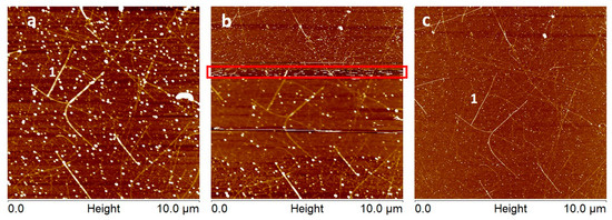
Figure 1.
Shows the process of attaching a CNT to an AFM tip using the high-force tapping mode imaging method. (a) is the image with the tip which is relatively blunt. (b) shows the process of attachment by reducing the imaging set-point until a resolution change is observed. (c) shows an improved resolution image with a stable CNT attached to the AFM tip. The height colour scale for images is 10 nm.
Analysis of the CNT in Figure 1a,c (denoted by the number 1) shows that the FWHM of the CNT has decreased by a factor of approximately 4 before and after CNT attachment.
This technique is particularly suited to the pick-up method as the same area can be re-scanned and the exact same CNTs FWHM compared before and after CNT attachment. A further advantage of high-force imaging is that it inevitably blunts the silicon AFM tips and, therefore, makes it obvious when CNT attachment has occurred. While this method is most applicable to the pick-up method it can also be used to verify CNT attachment using other techniques. Recent research has demonstrated that it is also possible to locate and relocate the same small areas and nanostructures on surfaces. This is typically done using techniques such as FIB milled or optical markers on the sample surface [26,72]. Tang et al. [48] also imaged and reimaged calibration grids before and after CNT attachment to demonstrate improved image resolution.
3.1.2. AVD Curves
Figure 2 shows a typical AVD curve when a CNT has been attached to an AFM tip. The figure shows sections A, B and C of the AVD curve. Section A shows where the AFM tip approaches the sample surface but has yet to contact it, therefore, the amplitude of cantilever oscillation is approximately zero and the curve is flat. Section B is where the tip begins to tap the surface and as the surface moves closer to the tip the amplitude of oscillation decreases steadily. Once the tapping force reaches a critical value the CNT begins to bend or buckle and the cantilever oscillation increases again and this is highlighted in section C. The amplitude and duration of the CNT buckling signature depends on a number of factors including the diameter of the CNT and the attached length [62,63,64,65]. This mode of operation is in-built in the majority of commercial AFMs and is relatively easy to implement with the primary drawback being that in the process of acquiring AVD curves the CNT can be dislodged if it is not securely attached. AVD curves have also been used to study experimentally and theoretically the compression, bending and overall mechanical behaviour of CNTs.
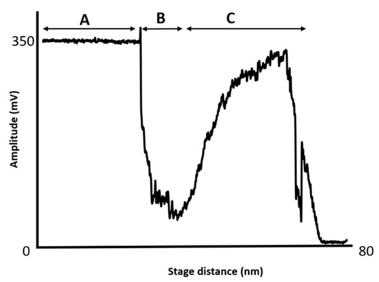
Figure 2.
This figure shows an AVD curve with a CNT attached. Section A is the tip approaching the surface with the amplitude of oscillation of the tip constant. Section B shows the amplitude of the cantilever as the tip begins to the tap the surface and the amplitude decreases. Section C shows where the CNT buckles and the amplitude of the cantilever temporarily increases until the amplitude is again suppressed.
3.1.3. Electron Microscopy (EM)
TEM and SEM are often used to determine CNT attachment but typically requires a high resolution field emission microscope to resolve the attached CNTs, particularly if they are less than 20 nm in diameter. Figure 3a–e are examples of SEM images of CNT-AFM tips produced using the pick-up method. While EM can produce definitive images of the attached CNTs potentially yielding information on tip shape, CNT diameter and CNT length they do require careful edge-on imaging with an experienced operator. The tips that the CNTs are attached to must also be conductive which can be problematic for silicon nitride tips. It should be noted that CNTs on AFM probes are also susceptible to changes in humidity and electrostatic forces [54] which may be experienced in preparing for and executing EM analysis. Wade et al. [54] noted that they could not produce TEM images of their AFM tips which they were confidant had CNTs attached using the pick-up method. They concluded that electrostatic charging was removing the CNTs from the AFM tips. They solved this by using AFM probe containers that were conductive. We have also found that the electron beam itself can, in some instances, cause the CNTs to move or detach from the AFM probe, making SEM imaging difficult and damaging to the CNT-AFM tip. This can be seen in Figure 3f where the CNT was originally in the position of the dotted line but during SEM imaging the CNT moved to its final position indicated in Figure 3f. This rendered the CNT tip unusable. It should be noted that for the AFM probes in Figure 3a–e SEM imaging was very stable and multiple images were acquired indicating secure CNT attachment to the AFM tip. These probes were suitable for extensive AFM imaging in standard tapping mode and as the tips they are attached to are conductive then potentially also conductive imaging. For most CNT attachment methods, including the pick-up technique, improved resolution and AVD curves are sufficient to verify CNT attachment has occurred.
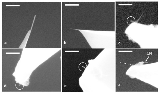
Figure 3.
SEM images of CNTs attached to AFM tips. The scale bars in each image are (a) 200 nm, (b) 500 nm, (c) 200 nm, (d) 200 nm, (e) 200 nm and (f) 200 nm. It can be seen in (f) that the electron beam moved the CNT from a relatively straight position, given by the dotted line, to a bent position.
3.2. CNT Attachment to Contact Mode Probe Using the Pick-Up Method and High-Force Imaging
Figure 4 shows tapping mode AFM images of the attachment process using high-force imaging and the pick-up method for a Bruker NP contact mode (Bruker Corporation, Billerica, MA, USA) with spring constant equal to 0.28 N/m [73]. Figure 4a shows that the image was very unstable which is due to the low spring constant of the contact mode cantilever causing the tip to adhere too strongly for the feedback to maintain stable imaging. The nominal diameter of these tips is 40 nm which is relatively large compared to standard tapping mode probes. However, in Figure 4a high force imaging was used and sections of the image show CNTs resolved which indicates CNT attachment is occurring.
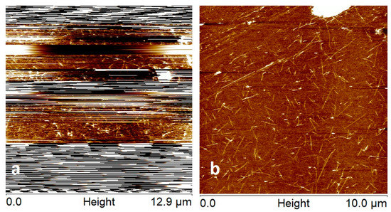
Figure 4.
(a) exhibits unstable imaging expected due to the low spring constant of the contact mode probe (0.28 N/m). High force imaging was used to attach a CNT to the AFM tip as can be seen in in sections of the image where CNTs are visible. (b) shows that CNT attachment was achieved due to a stable tapping mode image of the CNT surface. The height colour scale for images is 6 nm.
When CNT attachment was assumed to have taken place, which was confirmed by the AVD curve in Figure 5, then the probe was moved to a different location on the sample and a stable AFM image in tapping mode was achieved (refer to Figure 4b).
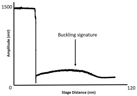
Figure 5.
Shows an AVD curve for the contact mode probe used to acquire the AFM images in Figure 4a,b. The buckling signature typical for CNT attachment can observed.
Stable tapping mode imaging with a contact mode probe is more likely after CNT attachment as the diameter of the CNT will be much less than the nominal diameter for the tip, thus reducing adhesion. Additionally, the stiffness of the CNT may add additional stability to the imaging process, provided the amplitude set-point is above 70–80% of the free cantilever amplitude. This is important as it demonstrates that modified high force imaging can facilitate CNT attachment to contact mode probes using the pick-up method. Therefore, since contact mode probes have spring constants 0.1–0.01 of the spring constant of standard tapping mode probes they can image soft materials with significantly reduced imaging force. This is the first time this technique has been used to attach CNTs to low spring constant contact mode probes.
3.3. CNT Attachment to Two Tapping Mode Probes Simultaneously Using the Pick-Up Method and High-Force Imaging
The pick-up method using high-force tapping mode imaging was applied to 1930-00 dlevers (Bruker Corporation, Billerica, MA, USA) which has two tapping mode AFM probes of the same length located on the same ship, with the nominal parameters described in Table 1. The methodology described in Section 2.3 was applied to these probes to demonstrate that the pick-up technique can be used to attach CNTs to more than 1 AFM probe simultaneously. An example of data indicating CNT attachment is shown in Figure 6a,b. This figure shows AVD curves acquired using 1930-00 dLever-C and 1930-00 dLever-D probes located on the same chip respectively. These AVD curves display distinctive buckling signatures indicating that CNT attachment has been achieved.
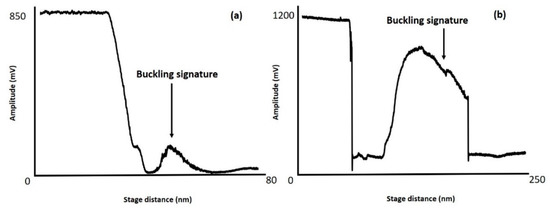
Figure 6.
Shows AVD curves for two 1930-00 dlever AFM probes located on the same chip using the procedure outlined in Section 2.3. (a) is for a 1930-00 dlever-C probe and (b) is for a 1930-00 dlever-D probe. Buckling signatures showing evidence of CNT attachment can be observed in both AVD curves.
To verify that the CNT attachment to both probes is stable tapping mode AFM images were acquired on the CNT covered substrate and are shown in Figure 7a,b.
Figure 7.
(a) and (b) Show tapping mode images with (a) acquired using a 1930-00 dlever-C probe and (b) acquired using a 1930-00 dlever-D probe. The height colour scale for both images is 5 nm.
In approximately 50% of attempts simultaneous CNT attachment was achieved demonstrating that the pick-up method, facilitated by high-force imaging, is capable of attachment to multiple AFM probes. This is another important result as it demonstrates the potential of the pick-up method to produce more than one CNT-AFM probe in a single process which has been a drawback of other techniques.
4. Discussion
Early indications of the routine use of CNT-AFM probes in AFM have not occurred and are due to a number of reasons including the difficulty in attaching CNTs to AFM tips, scaling up the attachment process to multiple probes, the tendency of CNT attachment methods to only be applied to high spring constant tapping mode probes and the technological development of silicon probes. While there are numerous techniques for attaching CNTs to AFM probes these methods are almost exclusively applied to one AFM tip at a time. Attaching CNTs to multiple AFM tips means that these types of probes could become more commonplace than they currently are. Indeed, very few manufacturers provide CNT-AFM probes and they are typically greater than 100 US dollars each (e.g., FN-1 series K-Tek Nanotechnology). In this work we demonstrate that the pick-up method, one of the simplest techniques to attach CNTs, can adhere CNTs to two AFM probes simultaneously. While this is not at the wafer scale it does demonstrate the proof of concept. There are a number of ways this technique can be improved. For example, by optimizing the CNT substrate and probe parameters such as spring constant. Carnally et al. [59] coated AFM tips with a thin film of plasma polymerized hexane before using the pick-up method to create CNT-AFM probes. This coating presents the CNT with a highly hydrophobic coating to which it can adsorb and improved the success rate and robustness of the CNT-AFM probes. This approach combined with the methods employed in this work could allow larger scale production of CNT-AFM probes and is the subject of further research. If this procedure could be scaled up then larger arrays of probes could be functionalized with CNTs with a wide range of applications including, but not limited to, providing the AFM community with high resolution durable probes and data storage density research.
In this work we also demonstrated that the pick-up method can be applied to contact mode probes with spring constant less than 0.30 N/m. CNT attachment allows these low spring constant probes to operate in tapping mode. Contact mode probes operating in tapping in air with attached CNTs will allow soft biological samples to be imaged with much less force than standard tapping mode probes, which have much higher spring constants.
We also reviewed the advantages and disadvantages of the different methods that can be used to detect CNT attachment which include improved image resolution, AVD curves and EM imaging. This will be useful for any scientists entering this area of research.
Funding
This research was partly funded by EPSRC Basic Technology Award (EP/C523857).
Acknowledgments
The author wishes to acknowledge Clive Roberts for useful discussions, Nicola Weston for assistance in acquiring SEM images, Stewart Carnally and Ashley Slattery for producing CNT covered substrates. The author also acknowledges the use and support of the South Australian node of Microscopy Australia at Flinders University, South Australia.
Conflicts of Interest
The author declares no conflict of interest.
References
- Zemła, J.; Danilkiewicz, J.; Orzechowska, B.; Pabijan, J.; Seweryn, S.; Lekka, M. Atomic force microscopy as a tool for assessing the cellular elasticity and adhesiveness to identify cancer cells and tissues. Semin. Cell Dev. Biol. 2018, 73, 115–124. [Google Scholar] [CrossRef] [PubMed]
- Bushell, G.R.; Cahill, C.; Clarke, F.M.; Gibson, C.T.; Myhra, S.; Watson, G.S. Imaging and force-distance analysis of human fibroblasts in vitro by atomic force microscopy. Cytom. Part A 1999, 36, 254–264. [Google Scholar] [CrossRef]
- Jeong, K.H.; Kim, K.S.; Lee, G.J.; Choi, S.J.; Jeong, T.J.; Shin, M.-K.; Park, H.K.; Sim, W.Y.; Lee, M.-H. Investigation of aging effects in human hair using atomic force microscopy. Skin Res. Technol. 2011, 17, 63–68. [Google Scholar] [CrossRef] [PubMed]
- Crossley, J.A.A.; Gibson, C.T.; Mapledoram, L.D.; Huson, M.G.; Myhra, S.; Pham, D.K.; Sofield, C.J.; Turner, P.S.; Watson, G.S. Atomic force microscopy analysis of wool fibre surfaces in air and under water. Micron 2000, 31, 659–667. [Google Scholar] [CrossRef]
- Bat-Erdene, M.; Batmunkh, M.; Shearer, C.J.; Tawfik, S.A.; Ford, M.J.; Yu, L.P.; Sibley, A.J.; Slattery, A.D.; Quinton, J.S.; Gibson, C.T.; et al. Efficient and fast synthesis of few-layer black phosphorus via microwave-assisted liquid-phase exfoliation. Small Methods 2017, 1, 1700260. [Google Scholar] [CrossRef]
- Prakash, G.; Capano, M.A.; Bolen, M.L.; Zemlyanov, D.; Reifenberger, R.G. AFM study of ridges in few-layer epitaxial graphene grown on the carbon-face of 4H-SiC(000(1) over-bar). Carbon 2010, 48, 2383–2393. [Google Scholar] [CrossRef]
- Pinto, G.; Canepa, P.; Canale, C.; Canepa, M.; Cavalleri, O. Morphological and Mechanical Characterization of DNA SAMs Combining Nanolithography with AFM and Optical Methods. Materials 2020, 13, 2888. [Google Scholar] [CrossRef]
- Thirlway, J.; Turner, I.J.; Gibson, C.T.; Gardiner, L.; Brady, K.; Allen, S.; Roberts, C.J.; Soultanas, P. DnaG interacts with a linker region that joins the N- and C-domains of DnaB and induces the formation of 3-fold symmetric rings. Nucleic Acids Res. 2004, 32, 2977–2986. [Google Scholar] [CrossRef]
- Gibson, C.T.; Ridings, C.R.; Blok, A.J.; Shearer, C.J.; Andersson, G.G.; Ellis, A.V. Morphological changes of sintered polydopamine coatings. Surf. Topogr. Metrol. Prop. 2019, 7, 015016. [Google Scholar] [CrossRef]
- Tonkin, S.J.; Gibson, C.T.; Campbell, J.; Lewis, D.A.; Karton, A.; Hasell, T.; Chalker, J.M. Chemically induced repair, adhesion, and recycling of polymers made by inverse vulcanization. Chem. Sci. 2020, 11, 5537–5546. [Google Scholar] [CrossRef]
- Bald, I.; Keller, A. Molecular Processes Studied at a Single-Molecule Level Using DNA Origami Nanostructures and Atomic Force Microscopy. Molecules 2014, 19, 13803–13823. [Google Scholar] [CrossRef] [PubMed]
- Anderson, M.S. The Detection of Long-Chain Bio-Markers Using Atomic Force Microscopy. Appl. Sci. 2019, 9, 1280. [Google Scholar] [CrossRef]
- Leite, F.L.; Bueno, C.C.; Da Róz, A.L.; Ziemath, E.C.; Oliveira, O.N., Jr. Theoretical Models for Surface Forces and Adhesion and Their Measurement Using Atomic Force Microscopy. Int. J. Mol. Sci. 2012, 13, 12773–12856. [Google Scholar] [CrossRef]
- Chen, L.; Zhao, X.; Pan, Y. Establishment of a Standard Method for Boundary Slip Measurement on Smooth Surfaces Based on AFM. Appl. Sci. 2019, 9, 1453. [Google Scholar] [CrossRef]
- Goreham, R.V.; Thompson, V.C.; Samura, Y.; Gibson, C.T.; Shapter, J.G.; Köper, I. Interaction of silver nanoparticles with tethered bilayer lipid membranes. Langmuir 2015, 31, 5868–5874. [Google Scholar] [CrossRef] [PubMed]
- Goudenhooft, C.; Siniscalco, D.; Arnould, O.; Bourmaud, A.; Sire, O.; Gorshkova, T.; Baley, C. Investigation of the Mechanical Properties of Flax Cell Walls during Plant Development: The Relation between Performance and Cell Wall Structure. Fibers 2018, 6, 6. [Google Scholar] [CrossRef]
- Spedden, E.; Staii, C. Neuron Biomechanics Probed by Atomic Force Microscopy. Int. J. Mol. Sci. 2013, 14, 16124–16140. [Google Scholar] [CrossRef]
- Slattery, A.D.; Blanch, A.J.; Ejov, V.; Quinton, J.S.; Gibson, C.T. Spring constant calibration techniques for next-generation fast-scanning atomic force microscope cantilevers. Nanotechnology 2014, 25, 335705. [Google Scholar] [CrossRef]
- Ando, T.; Uchihashi, T.; Kodera, N.; Yamamoto, D.; Miyagi, A.; Taniguchi, M.; Yamashita, H. High-speed AFM and nano-visualization of biomolecular processes. Pflug. Arch. 2008, 456, 211–225. [Google Scholar] [CrossRef]
- Hinterdorfer, P.; Dufrene, Y.F. Detection and localization of single molecular recognition events using atomic force microscopy. Nat. Methods 2006, 3, 347–355. [Google Scholar] [CrossRef]
- Creasey, R.; Sharma, S.; Craig, J.E.; Gibson, C.T.; Ebner, A.; Hinterdorfer, P.; Voelcker, N.H. Detecting protein aggregates on untreated human tissue samples by atomic force microscopy recognition imaging. Biophys. J. 2010, 99, 1660–1667. [Google Scholar] [CrossRef] [PubMed]
- Creasey, R.; Sharma, S.; Gibson, C.T.; Craig, J.E.; Ebner, A.; Becker, T.; Hinterdorfer, P.; Voelcker, N.H. Atomic force microscopy-based antibody recognition imaging of proteins in the pathological deposits in pseudoexfoliation syndrome. Ultramicroscopy 2011, 111, 1055–1061. [Google Scholar] [CrossRef] [PubMed]
- Rung, S.; Schwarz, S.; Götzendorfer, B.; Esen, C.; Hellmann, R. Time Dependence of Wetting Behavior Upon Applying Hierarchic Nano-Micro Periodic Surface Structures on Brass Using Ultra Short Laser Pulses. Appl. Sci. 2018, 8, 700. [Google Scholar] [CrossRef]
- Shearer, C.J.; Slattery, A.D.; Stapleton, A.J.; Shapter, J.G.; Gibson, C.T. Accurate thickness measurement of graphene. Nanotechnology 2016, 27, 125704. [Google Scholar] [CrossRef] [PubMed]
- Slattery, A.D.; Blanch, A.J.; Shearer, C.J.; Stapleton, A.J.; Goreham, R.V.; Harmer, S.L.; Quinton, J.S.; Gibson, C.T. Characterisation of the Material and Mechanical Properties of Atomic Force Microscope Cantilevers with a Plan-View Trapezoidal Geometry. Appl. Sci. 2019, 9, 2604. [Google Scholar] [CrossRef]
- Slattery, A.D.; Blanch, A.J.; Quinton, J.S.; Gibson, C.T. Calibration of atomic force microscope cantilevers using standard and inverted static methods assisted by FIB-milled spatial markers. Nanotechnology 2013, 24, 015710. [Google Scholar] [CrossRef] [PubMed]
- Slattery, A.D.; Blanch, A.J.; Quinton, J.S.; Gibson, C.T. Accurate measurement of atomic force microscope cantilever deflection excluding tip-surface contact with application to force calibration. Ultramicroscopy 2013, 131, 46–55. [Google Scholar] [CrossRef]
- Higgins, M.J.; Proksch, R.; Sader, J.E.; Polcik, M.; Cleveland, J.P.; Jarvis, S.P. Noninvasive determination of optical lever sensitivity in atomic force microscopy. Rev. Sci. Instrum. 2006, 77, 013701. [Google Scholar] [CrossRef]
- Flater, E.E.; Zacharakis-Jutz, G.E.; Dumba, B.G.; White, I.A.; Clifford, C.A. Towards easy and reliable AFM tip shape determination using blind tip reconstruction. Ultramicroscopy 2014, 146, 130–143. [Google Scholar] [CrossRef]
- Zeng, Z.; Zhu, G.; Guo, Z.; Zhang, L.; Yan, X.; Du, Q.; Liu, R. A simple method for AFM tip characterization by polystyrene spheres. Ultramicroscopy 2008, 108, 975–980. [Google Scholar] [CrossRef]
- Wang, J.; Qiao, W.; Mu, X. Au Tip-Enhanced Raman Spectroscopy for Catalysis. Appl. Sci. 2018, 8, 2026. [Google Scholar] [CrossRef]
- Bazylewski, P.; Ezugwu, S.; Fanchini, G. A Review of Three-Dimensional Scanning Near-Field Optical Microscopy (3D-SNOM) and Its Applications in Nanoscale Light Management. Appl. Sci. 2017, 7, 973. [Google Scholar] [CrossRef]
- Ruffino, F.; Grimaldi, M.G. Morphological Characteristics of Au Films Deposited on Ti: A Combined SEM-AFM Study. Coatings 2018, 8, 121. [Google Scholar] [CrossRef]
- Fernandes, J.P.C.; Mareau, V.H.; Gonon, L. AFM-Raman colocalization setup: Advanced characterization technique for polymers. Int. J. Polym. Anal. Charact. 2018, 23, 113. [Google Scholar] [CrossRef]
- Dresselhaus, S.; Dresselhaus, G.; Avouris, P. Carbon Nanotubes: Synthesis, Structure, Properties, and Applications, 1st ed.; Springer: Berlin/Heidelberg, Germany, 2001; pp. 1–448. [Google Scholar]
- Grace, T.; Pham, H.D.; Gibson, C.T.; Shapter, J.G.; Sonar, P. Application of A Novel, Non-Doped, Organic Hole-Transport Layer into Single-Walled Carbon Nanotube/Silicon Heterojunction Solar Cells. Appl. Sci. 2019, 9, 4721. [Google Scholar] [CrossRef]
- Alzahly, S.; Yu, L.; Shearer, C.J.; Gibson, C.T.; Shapter, J.G. Efficiency Improvement Using Molybdenum Disulphide Interlayers in Single-Wall Carbon Nanotube/Silicon Solar Cells. Materials 2018, 11, 639. [Google Scholar] [CrossRef]
- Min, C.; He, Z.; Song, H.; Liu, D.; Jia, W.; Qian, J.; Jin, Y.; Guo, L. Fabrication of Novel CeO2/GO/CNTs Ternary Nanocomposites with Enhanced Tribological Performance. Appl. Sci. 2019, 9, 170. [Google Scholar] [CrossRef]
- Yuan, S.; Bai, J.; Chua, C.K.; Wei, J.; Zhou, K. Material Evaluation and Process Optimization of CNT-Coated Polymer Powders for Selective Laser Sintering. Polymers 2016, 8, 370. [Google Scholar] [CrossRef]
- Kim, S. CNT Sensors for Detecting Gases with Low Adsorption Energy by Ionization. Sensors 2006, 6, 503–513. [Google Scholar] [CrossRef]
- Wang, L.-C.; Tang, K.-T.; Teng, I.-J.; Kuo, C.-T.; Ho, C.-L.; Kuo, H.-W.; Su, T.-H.; Yang, S.-R.; Shi, G.-N.; Chang, C.-P. A Single-Walled Carbon Nanotube Network Gas Sensing Device. Sensors 2011, 11, 7763–7772. [Google Scholar] [CrossRef]
- Ma, L.; Dong, X.; Chen, M.; Zhu, L.; Wang, C.; Yang, F.; Dong, Y. Fabrication and Water Treatment Application of Carbon Nanotubes (CNTs)-Based Composite Membranes: A Review. Membranes 2017, 7, 16. [Google Scholar] [CrossRef] [PubMed]
- Das, R.; Ali, M.E.; Hamid, S.B.A.; Ramakrishna, S.; Chowdhury, Z.Z. Carbon nanotube membranes for water purification: A bright future in water desalination. Desalination 2014, 336, 97–109. [Google Scholar] [CrossRef]
- Slattery, A.D.; Blanch, A.J.; Quinton, J.S.; Gibson, C.T. Efficient attachment of carbon nanotubes to conventional and high-frequency AFM probes enhanced by electron beam processes. Nanotechnology 2013, 24, 235705. [Google Scholar] [CrossRef] [PubMed]
- Cheung, C.L.; Hafner, J.H.; Lieber, C.M. Carbon nanotube atomic force microscopy tips: Direct growth by chemical vapor deposition and application to high resolution imaging. Proc. Natl. Acad. Sci. USA 2000, 97, 3809–3813. [Google Scholar] [CrossRef] [PubMed]
- Hafner, J.H.; Cheung, C.L.; Lieber, C.M. Direct Growth of Single-Walled Carbon Nanotube Scanning Probe Microscopy Tips. J. Am. Chem. Soc. 1999, 121, 9750–9751. [Google Scholar] [CrossRef]
- Slattery, A.D.; Shearer, C.J.; Shapter, J.G.; Quinton, J.S.; Gibson, C.T. Solution based methods for the fabrication of carbon nanotube modified atomic force microscopy probes. Nanomaterials 2017, 7, 346. [Google Scholar] [CrossRef]
- Tang, J.; Yang, G.; Zhang, Q.; Parhat, A.; Maynor, B.; Liu, J.; Qin, L.C.; Zhou, O. Rapid and reproducible fabrication of carbon nanotube AFM probes by dielectrophoresis. Nano Lett. 2005, 5, 11–14. [Google Scholar] [CrossRef]
- Chin, S.-C.; Chang, Y.-C.; Chang, C.-S. The fabrication of carbon nanotube probes utilizing ultra-high vacuum transmission electron microscopy. Nanotechnology 2009, 20, 285307. [Google Scholar] [CrossRef]
- Shin, Y.H.; Song, J.W.; Lee, E.S.; Han, C.S. Imaging characterization of carbon nanotube tips modified using a focused ion beam. Appl. Surf. Sci. 2007, 253, 6872–6877. [Google Scholar] [CrossRef]
- Strus, M.C.; Raman, A.; Han, C.-S.; Nguyen, C.V. Imaging artefacts in atomic force microscopy with carbon nanotube tips. Nanotechnology 2005, 16, 2482. [Google Scholar] [CrossRef]
- Larsen, T.; Moloni, K.; Flack, F.; Eriksson, M.A.; Lagally, M.G.; Black, C.T. Comparison of wear characteristics of etched-silicon and carbon nanotube atomic force microscopy probes. Appl. Phys. Lett. 2002, 80, 1996. [Google Scholar] [CrossRef]
- Su, C.; Huang, L.; Kjoller, K.; Babcock, K. Studies of tip wear processes in tapping mode atomic force microscopy. Ultramicroscopy 2003, 97, 135–144. [Google Scholar] [CrossRef]
- Slattery, A.D.; Shearer, C.J.; Gibson, C.T.; Shapter, J.G.; Lewis, D.A.; Stapleton, A.J. Carbon nanotube modified probes for stable and high sensitivity conductive atomic force microscopy. Nanotechnology 2016, 27, 475708. [Google Scholar] [CrossRef] [PubMed]
- Martinez, J.; Yuzvinsky, T.D.; Fennimore, A.M.; Zettl, A.; Garcia, R.; Bustamante, C. Length control and sharpening of atomic force microscope carbon nanotube tips assisted by an electron beam. Nanotechnology 2005, 16, 2493. [Google Scholar] [CrossRef]
- Dremov, V.; Fedoseev, V.; Fedorov, P.; Grebenko, A. Fast and reliable method of conductive carbon nanotube-probe fabrication for scanning probe microscopy. Rev. Sci. Instrum. 2015, 86, 053703. [Google Scholar] [CrossRef]
- Xua, J.; Shingaya, Y.; Zhao, Y.; Nakayama, T. In situ, controlled and reproducible attachment of carbon nanotubes onto conductive AFM tips. Appl. Surf. Sci. 2015, 335, 11. [Google Scholar] [CrossRef]
- Hafner, J.H.; Cheung, C.-L.; Oosterkamp, T.H.; Lieber, C.M. High-Yield Assembly of Individual Single-Walled Carbon Nanotube Tips for Scanning Probe Microscopies. J. Phys. Chem. B 2001, 105, 743–746. [Google Scholar] [CrossRef]
- Carnally, S.; Barrow, K.; Alexander, M.R.; Hayes, C.J.; Stolnik, S.; Tendler, S.J.B.; Williams, P.M.; Clive, J.; Roberts, C.J. Ultra-resolution imaging of a self-assembling biomolecular system using robust carbon nanotube AFM probes. Langmuir 2007, 23, 3906–3911. [Google Scholar] [CrossRef]
- Wade, L.A.; Shapiro, I.R.; Ma, Z.; Quake, S.R.; Collier, C.P. Correlating AFM Probe Morphology to Image Resolution for Single-Wall Carbon Nanotube Tips. Nano Lett. 2004, 4, 725–731. [Google Scholar] [CrossRef]
- Gibson, C.T.; Carnally, S.; Roberts, C.J. Attachment of carbon nanotubes to atomic force microscope probes. Ultramicroscopy 2007, 107, 1118–1122. [Google Scholar] [CrossRef]
- Slattery, A.D.; Shearer, C.J.; Shapter, J.G.; Blanch, A.J.; Quinton, J.S.; Gibson, C.T. Improved Application of Carbon Nanotube Atomic Force Microscopy Probes Using PeakForce Tapping Mode. Nanomaterials 2018, 8, 807. [Google Scholar] [CrossRef] [PubMed]
- Vettiger, P.; Despont, M.; Drechsler, U.; Durig, U.; Haberle, W.; Lutwyche, M.I.; Rothuizen, H.E.; Stutz, R.; Widmer, R.; Binnig, G.K. The Millipede—More than thousand tips for future AFM storage. IBM J. Res. Dev. 2000, 44, 323–340. [Google Scholar] [CrossRef]
- King, W.P.; Kenny, T.W.; Goodson, K.E.; Cross, G.; Despont, M.; Dürig, U.; Rothuizen, H.; Binnig, G.K.; Vettiger, P. Atomic force microscope cantilevers for combined thermomechanical data writing and reading. Appl. Phys. Lett. 2001, 78, 1300–1302. [Google Scholar] [CrossRef]
- Hu, H.; Kim, H.J.; Somnath, S. Tip-Based Nanofabrication for Scalable Manufacturing. Micromachines 2017, 8, 90. [Google Scholar] [CrossRef]
- Haq, E.U.; Liu, Z.; Zhang, Y.; Ahmad, S.A.A.; Wong, L.-S.; Armes, S.P.; Hobbs, J.K.; Leggett, G.J.; Micklefield, J.; Roberts, C.J.; et al. Parallel scanning near-field photolithography: The snomipede. Nano Lett. 2010, 10, 4375–4380. [Google Scholar] [CrossRef]
- Dürig, U.; Cross, G.; Despont, M.; Drechsler, U.; Häberle, W.; Lutwyche, M.I.; Rothuizen, H.; Stutz, R.; Widmer, R.; Vettiger, P.; et al. “Millipede”—An AFM data storage system at the frontier of nanotribology. Tribol. Lett. 2000, 9, 25–32. [Google Scholar]
- Li, J.; Cassell, A.M.; Hongjie, D. Carbon nanotubes as AFM tips: Measuring DNA molecules at the liquid/solid interface. Surf. Interface Anal. 1999, 28, 8–11. [Google Scholar] [CrossRef]
- Hu, X.; Wei, H.; Deng, Y.; Chi, X.; Liu, J.; Yue, J.; Peng, Z.; Cai, J.; Jiang, P.; Sun, L. Amplitude response of conical multiwalled carbon nanotube probes for atomic force microscopy. RSC Adv. 2019, 9, 429–434. [Google Scholar] [CrossRef]
- Kutana, A.; Giapis, K.P.; Chen, J.Y.; Collier, C.P. Amplitude response of single-wall carbon nanotube probes during tapping mode atomic force microscopy: Modeling and experiment. Nano Lett. 2006, 6, 1669–1673. [Google Scholar] [CrossRef]
- Nguyen, C.V.; Chao, K.J.; Stevens, R.M.D.; Delzeit, L.; Cassell, A.; Han, J.; Meyyappan, M. Carbon nanotube tip probes: Stability and lateral resolution in scanning probe microscopy and application to surface science in semiconductors. Nanotechnology 2001, 12, 363–367. [Google Scholar] [CrossRef]
- Jones, D.B.; Chen, X.; Sibley, A.; Quinton, J.S.; Shearer, C.J.; Gibson, C.T.; Raston, C.L. Plasma enhanced vortex fluidic device manipulation of graphene oxide. Chem. Commun. 2016, 52, 10755–10758. [Google Scholar] [CrossRef] [PubMed]
- Sader, J.E.; Borgani, R.; Gibson, C.T.; Haviland, D.B.; Higgins, M.J.; Kilpatrick, J.I.; Lu, J.; Mulvaney, P.; Shearer, C.J.; Slattery, A.D.; et al. A virtual instrument to standardise the calibration of atomic force microscope cantilevers. Rev. Sci. Instrum. 2016, 87, 093711. [Google Scholar] [CrossRef] [PubMed]
© 2020 by the author. Licensee MDPI, Basel, Switzerland. This article is an open access article distributed under the terms and conditions of the Creative Commons Attribution (CC BY) license (http://creativecommons.org/licenses/by/4.0/).