1. Introduction
The ongoing miniaturization of modern engineering systems amplifies the need to deliver multifunctional performance with limited power, weight and volume budgets. To overcome these challenges, researchers have relied increasingly on multifunctional materials, whose properties can be controlled and triggered by various external stimuli, such as stress, electric or magnetic fields, and temperature. These smart materials integrate different functionalities within their structure, thereby eliminating the need for auxiliary units in volume-limited applications. They have enabled new design options and are now widely used across a range of fields, including soft robotics [
1,
2], aerospace engineering [
3,
4] and microelectromechanical systems (MEMS) [
5]. Smart materials, especially phase change materials (PCMs), are also frequently used in actuators, i.e., devices that convert one form of energy into movement or mechanical work. Among different actuation principles, such as piezoelectrics, shape memory effects and electrostriction, paraffin-based phase change microactuators represent an innovative alternative to conventional, structurally rigid actuators [
6].
Paraffin-based actuators utilize commercially available, chemically inert and inexpensive compounds that exhibit high mechanical energy densities (105–108 J/m3). The most common actuating principle involves heating the paraffin wax until its melting, a process which is correlated to a volume increase of 15–20%. This volumetric expansion can drive a mechanical element, such as a piston or a flexible membrane, thereby fulfilling a mechanical task. Despite showing large strokes relative to the actuating material volume, paraffin actuators are usually slow, due to the low thermal conductivity (0.2–0.3 W/m K) of the PCM, which prevents their use in applications requiring rapid actuation.
To overcome this limitation, researchers have experimented with different approaches. Some groups [
7,
8,
9] added thermally conductive particles to the paraffin wax to increase the overall thermal conductivity or to make the actuators sensitive to new stimuli, such as an electric or magnetic field. Other groups [
10,
11,
12] focused on designing leakage-free structures that can hold liquid paraffin via surface tension forces. Similarly, Mann et al. [
13] investigated strategies to increase the mechanical output of paraffin actuators, reaching a significant work output of 659 kJ/m
3. Despite these efforts, most of these actuators are still slower than other smart actuator, and they are monofunctional, employing paraffin only for actuation and preventing any multifunctional coupling.
Recently, a new strategy to both control the actuation speed and introduce additional features to paraffin actuators has been proposed by our group [
14,
15]. In our research, we integrated paraffin actuators with thermoelectric generators (TEGs), devices that can benefit from the Seebeck effect to transform thermal energy into electric energy or exploit the Peltier effect for actuating through confined heating or cooling. The presence of a thermoelectric element enables actuation via heating and also reduces the reset time via active cooling (up to 80% compared to passive cooling), thus enhancing the cycle rate of the actuator [
15,
16]. Yet, part of the thermal energy is still lost at the interface between the thermoelectric component and the paraffin actuator, and these systems cannot be tailored to specific needs, since the paraffin actuator size is constrained by the size of the commercially available TEGs. To address these limitations, recent research has shifted towards the development of highly integrated thermal architectures.
Besides conventional planar thermoelectric devices, alternative architectures based on multilayer substrates have also been investigated. Initial studies on thick-film technology demonstrated that functional components, including resistors and thermistors, could be fabricated directly within the vias of ceramic or polymer substrates [
17]. This concept was further developed by Markowski and Dziedzic [
18], who reported the first practical realization of a 3D thermoelectric microgenerator in Low-Temperature Co-fired Ceramics (LTCC) by filling neighboring vias with thermocouple materials. Subsequent studies, including our previous work, have expanded these concepts to PCB-based fabrication processes, allowing the manufacturing of scalable µTEG [
19]. However, although these substrate-integrated approaches have successfully demonstrated thermoelectric energy generation, limited attention has been given to their integration with phase change materials and actuation mechanisms.
In this work, we present a scalable fabrication strategy for a quasi-monolithic all-in-one integrated TEG-PCM actuator system using standard four-layer printed circuit board (PCB) technology. Similar to our previous systems, this design has a dual functionality. It can function as a paraffin microactuator, when power is provided to the TEG, using the device as a Peltier element. Alternatively, the TEG can harvest thermal energy available from the surrounding environment through the PCM interface. The design uses a four-layer PCB, with the first two copper layers forming the paraffin actuator, and the remaining two layers for the TEG. This design enhances internal heat transfer and ensures structural integration, thus optimizing the interaction between the TEG and the paraffin actuator.
The proposed quasi-monolithic integration strategy can be expanded to a wide range of thermoelectric-based applications. By eliminating bulky thermal interfaces, this architecture is highly relevant for systems requiring high power density and compactness. In the automotive sector, for example, where TEG recover waste heat from exhaust systems, a monolithic-inspired design could minimize thermal interface losses, which currently bottleneck conversion efficiency [
20]. Similarly, by integrating energy harvesting and actuation, this technology is well-suited for wearable devices and self-powered sensor systems, where size and energy constraints are critical [
21,
22]. Furthermore, the precise thermal control enabled by integrated PCM layers offers a robust solution for microelectronic thermal management [
23]. These systems provide a buffer against transient heat loads while maintaining a slim profile. These examples demonstrate the potential of the proposed approach as a versatile platform for multifunctional and thermally efficient systems.
2. Materials and Methods
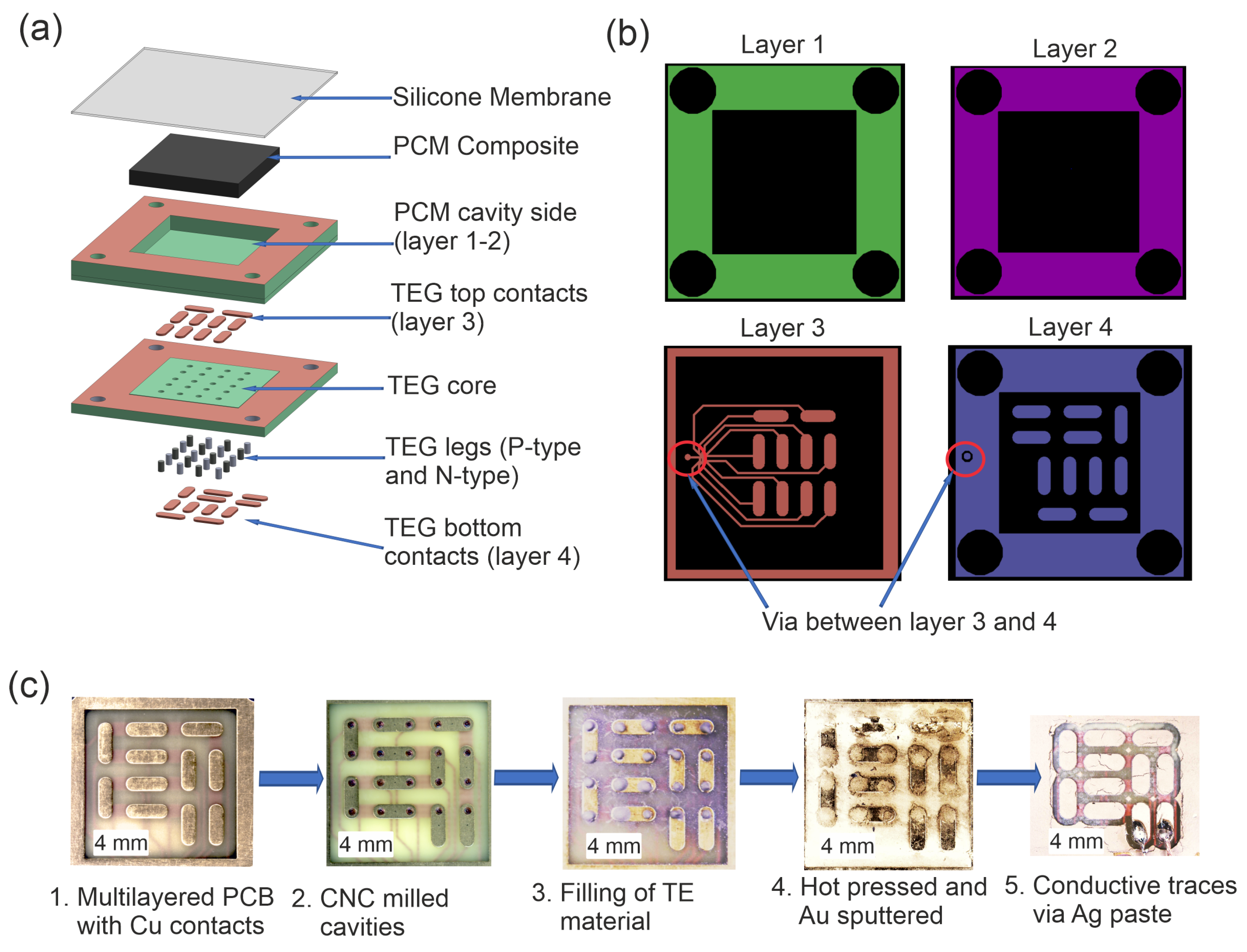
Figure 1a illustrates the design and concept of the integrated TEG-PCM system. The system is divided into two sections. The upper level (layers 1 and 2, see
Figure 1b) is intended for the PCM storage and actuation functions, and it is sealed by a silicone membrane to prevent leakage. The bottom level (layers 3 and 4,
Figure 1b) operates as a TEG or a Peltier element, depending on the operating mode. In TEG mode, the thermoelectric module converts a temperature difference across the device into electrical power via the Seebeck effect. In Peltier mode, an applied electrical current induces controlled heating or cooling of the PCM layer.
The initial four-layer PCB intended for the TEG-PCM system (step 1 in
Figure 1c) was designed and produced by Multi Leiterplatten GmbH, Brunnthal - Hofolding, Germany. The PCB’s architecture incorporates features to support the further fabrication of the TEG-PCM system. The four-layer PCB consists of four 70 µm copper layers alternating with three FR4 layers as a substrate. The total PCB thickness is 1.55 mm and it measures 20 mm × 20 mm. The two topmost layers (1 and 2, see
Figure 1b) were milled to half the PCB thickness to create a sealed container for the PCM material. Layers 3 and 4 (see
Figure 1b) were patterned to form conductive traces for a vertical TEG, with the thermoelectric material forming the conductive pathway between these two layers.
After PCB production, 20 cavities with a diameter of 500 µm were micro-machined into the substrate (step 2 in
Figure 1c) using a CNC milling system (Bungard Elektronik GmbH, Windeck, Germany). To achieve accurate depth control, the milling was carried out from the bottom contact (layer 4) to the internal contact (layer 3) of the TEG. An electrical sensing via (detail in
Figure 1b) was used to detect when Layer 3 was reached: the milling bit and the internal copper layer acted as a switch that closed a sensing circuit upon contact, triggering an automatic stop. This hardware-based feedback ensures a vertical precision of approximately ±3.175 µm, which is essential to preserve the integrity of the underlying thermoelectric tracks. This approach ensured a uniform cavity depth prior to the deposition of the thermoelectric material.
The micro-machined holes were then filled with P-type (
) and N-type (
) thermoelectric (TE) materials (step 3 in
Figure 1c), which were selected for their high figure of merit (
) at room temperature [
24,
25]. These materials were prepared from 99.999% pure bismuth, tellurium, antimony and selenium (Merck, Darmstadt, Germany). The starting materials were mixed in stoichiometric ratios and mechanically alloyed using a high-energy ball mill from Retsch, Haan, Germany. Ball milling was operated for 4.5 h at 1000 rpm with a 1 min pause every 10 min to prevent overheating. The TE alloys were then filtered through a sieve with a mesh size of 63 µm using the AS 200 Basic sieve shaker from Retsch, Germany, for 30 min. The filtered material was then mixed with Terpineol (Merck, Germany) in a 9:1 ratio using a mortar and pestle. The resulting paste was then transferred to a syringe and dispensed manually into the holes.
Two filling steps were necessary, each followed by heating on a hot plate at 80 °C to evaporate the solvent. The four-layer PCB sample was hot pressed at 2.5 kN to compact the TE material. During the hot pressing, the samples were gradually heated from 100 °C to 175 °C in 25 °C steps. Each increment was held for 10 min. Following this, gold sputter deposition was carried out on the TEG legs and copper contacts to reduce the contact resistance between copper and the TE materials (step 4 in
Figure 1c). A layer of silver paste from Nanografi Nano Technology, Turkey, was then applied to the gold-sputtered surface using a doctor blade applicator. The samples were then cured in the oven at 135 °C for 35 min. This layer was used to prevent oxidation of the TE material and minimizes the contact resistance between the two materials. The contact pads were then isolated using a CNC mill. Two wires were then connected to the edges of the TE path (step 5 in
Figure 1c). A total of three devices were fabricated and tested to validate the architecture’s functional feasibility, a priority for prototype systems before full experimental characterization [
26,
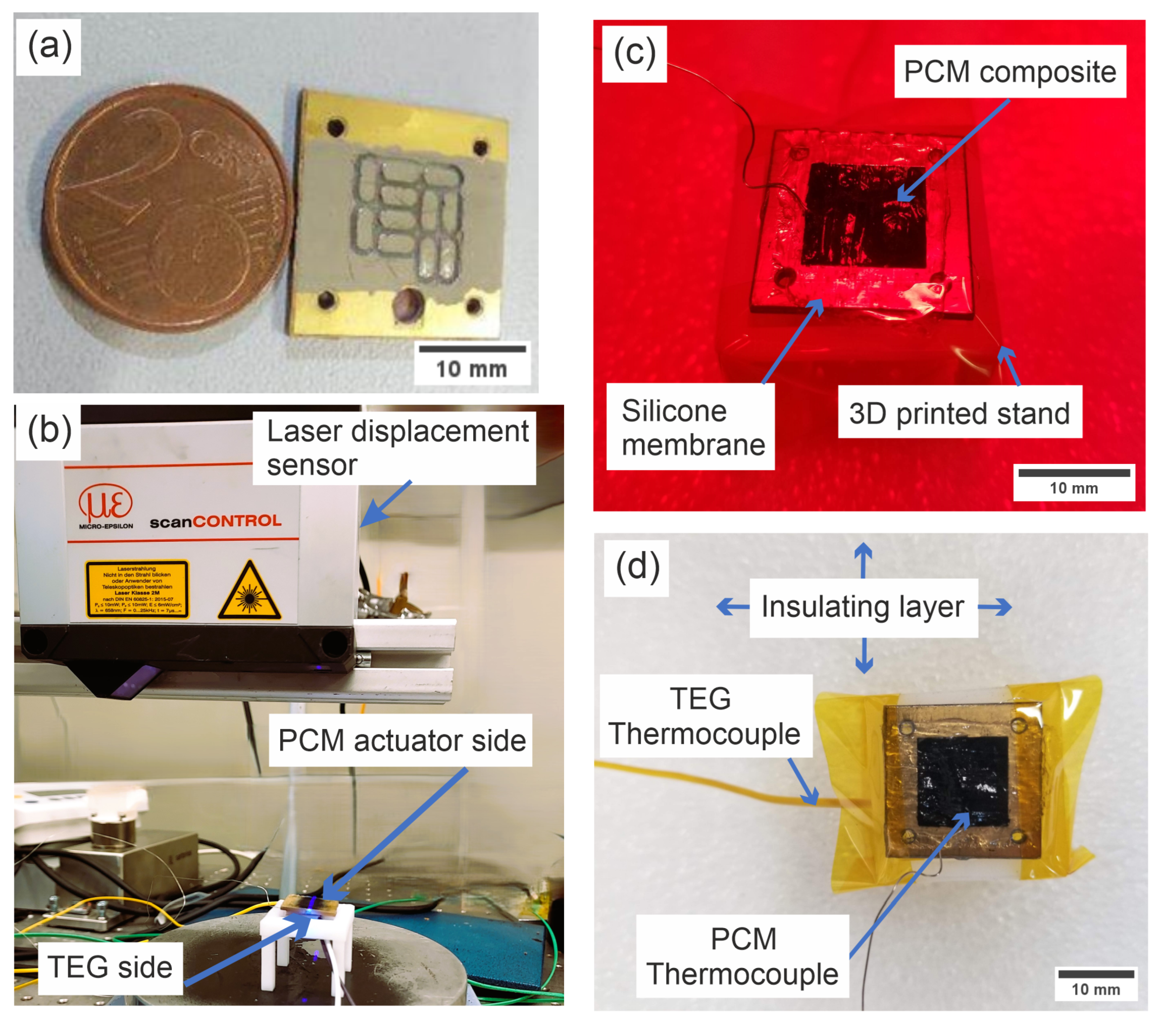
27]. The TEG sample prior to wiring is shown in
Figure 2a.
The paraffin wax employed for the actuator was procured from Rubitherm Technologies GmbH, Germany and had a melting point of 42 °C and a latent heat of
J/g. To increase the thermal conductivity of the paraffin wax, it was blended with 2 wt% of graphene nanoplatelets (GnPs) with a purity of 99.9 %, average diameter of 18 µm and a thickness of 5 nm, ordered from Nanografi Nano Technology, Turkey. At this low loading, the addition of graphene is reported to have a negligible effect on the melting temperature, while mainly improving thermal conductivity [
28]. The PCM composite was synthesized via the mixing-melting method, as described by Laouer et al. [
15,
29]. Approximately 180 µL of PCM composite was filled into the milled cavity on top of the PCB in its solid state and sealed with a silicone sealant (DOWSIL™ 732 from Dow Chemical Company, Midland, MI, USA). This was spread on the PCM composite side, forming a wet membrane of approximately 150 µm. This material exhibits a Shore A = 25 and tensile strength = 2.3 MPa, corresponding to an estimated Young modulus of 0.95 ± 50% MPa [
30]. The system was then left overnight at room temperature (23 °C) to cure the sealant.
The deflection of the PCM actuator membrane was monitored using a scanControl 3002-25/BL 2D laser profile scanner (
Figure 2b) from Micro-Epsilon Messtechnik GmbH & Co. KG (Ortenburg, Germany). The actuating force was assessed using an 8-mm S1-10N sensor from PPS UK Ltd., Glasgow, UK, which was placed on top of the PCM cavity. The energy harvesting properties of the device were quantified by mimicking a 20-min “day–night” cycle, consisting of 10 min of heating and 10 min of cooling (
Figure 2c). The heat source employed was a 250 W infrared (IR) lamp produced by Philips, the Netherlands. The lamp was placed 25 cm away from the device to prevent overheating.
A 3D-printed stand was manufactured using a stereolithography printer (Form 3+, Formlabs, Somerville, MA, USA) to increase air circulation and enhance natural convection at the bottom TEG level. Two thermocouples were placed within the PCM cavity, before it was sealed, and at the bottom side of the TEG layer (
Figure 2c,d). The thermocouples were linked to a temperature logger from Testo SE & Co. KGaA, Titisee-Neustadt, Germany to collect the data.
3. Results
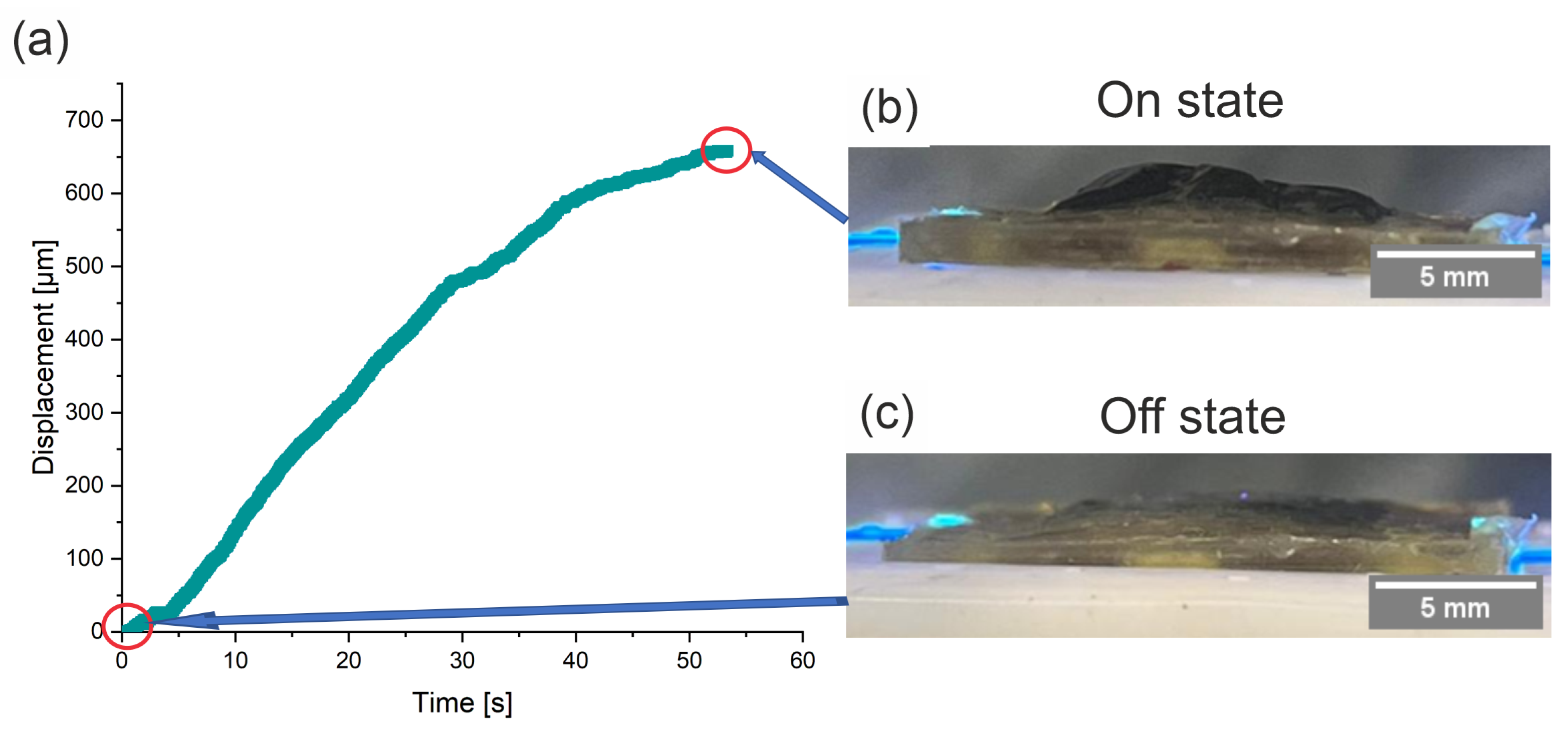
The response of the TEG-PCM actuator was evaluated by monitoring the membrane displacement over a period of 55 s, as shown in
Figure 3a.
The input power supplied to the TEG was approximately 1 W, corresponding to 10 V and 0.1 A. Upon heating, the membrane displayed a consistent linear increase in displacement during the initial 30 s, reaching 482 µm. Afterwards, the displacement curve showed a slight deceleration, peaking at 658 µm after 55 s. The volumetric phase transition from the solid to liquid state is displayed in
Figure 3b,c. In the off state (
Figure 3b), the membrane is planar with a low profile. Conversely, after heating, the membrane undergoes deformation and stretching due to the pressure exerted by the PCM composite. The expansion is relatively uniform, although some regions exhibit slightly higher displacement. Similar actuation behavior was observed across the tested devices, with comparable displacement trends (average maximum displacement of
µm). To quantify the mechanical work capacity of the TEG-PCM system, the blocking force was measured during the TEG heating process by placing the force sensor in contact with the actuator at the initial time
s, ensuring zero-displacement conditions. The maximum force generated by the actuator was 190 mN. The force output followed a trend consistent with the visual data. This indicates the system’s ability to convert PCM-induced pressure into mechanical work. Furthermore, this consistency establishes functional stability which is beneficial for extensive experimental investigations.
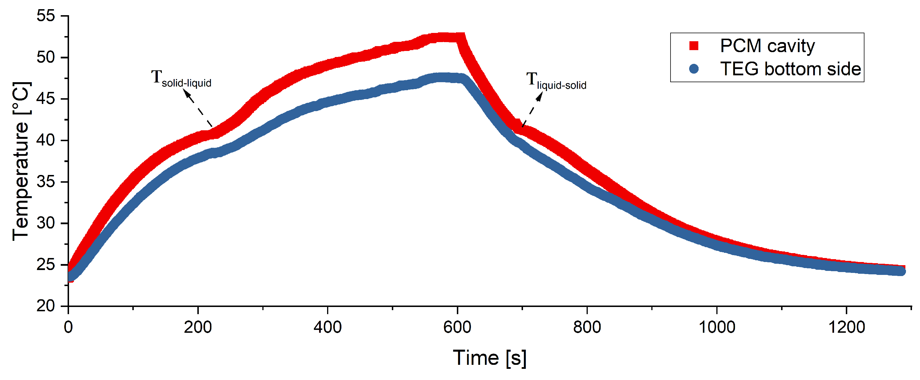
The thermal energy harvesting and storage properties of the TEG-PCM system were evaluated from the temperature difference between the PCM cavity and the bottom side of the TEG, as shown in
Figure 4. In the experiment, the IR lamp was switched on at
s and turned off after 10 min (
s). At the beginning, for approximately 230 s, the two curves showed no significant influence of the PCM composite on the overall system. The directional heating resulted in a temperature difference of approximately 2.5 K between the two TEG sides. The temperature profile showed a change in slope at around 41 °C and the temperature difference between the top and bottom TEG faces began to increase. The curves continued to rise up to 600 s, corresponding to a temperature difference of ∼5 K. At this point, the top and bottom sides of the TEG reached a maximum temperature of 52.4 °C and 47.5 °C, respectively. After 600 s, the IR lamp was turned off. The two sides of the TEG-PCM system began to cool down, showing a change in slope at approximately 41 °C. The two sides continued cooling and eventually returned to room temperature.
4. Discussion
The actuation curve in
Figure 3a shows the effective conversion of electrical energy into the thermal energy needed for the volumetric phase change in the PCM composite. After heating the PCM cavity for a couple of seconds, the system enters a steady-state regime and the displacement increases linearly at a rate of approximately:
After 30 s, the PCM actuation slows down to a level of 7.6 µm/s. The reduction in slope is mainly attributed to the establishment of thermomechanical equilibrium between the volumetric expansion of the paraffin composite and the elastic membrane’s counteracting force. After the paraffin wax is completely melted, the volumetric expansion reaches a plateau.
This result can be compared with our previous design, consisting of a 10 mm × 10 mm × 3 mm aluminum block integrated with a 9 mm × 9 mm × 9 mm commercial TEG (see [
15] for a more detailed description of the assembly). Using the same paraffin formulation, the two-piece design heated a PCM amount of 18.18 µL with an input power of 1.98 W, reaching a maximum displacement of 547 µm in 64 s. The displacement rate corresponds to
= 8.55 µm/s. The current all-in-one system can achieve the same amount of displacement in a shorter time (36.4 s) and with less input power (1 W). This corresponds to a displacement rate of
= 15.03 µm/s. Such findings indicate a ∼76% increase in displacement rate with nearly half the input power. However, the observed performance shift, specifically the reduction in blocking force, reflects the different mechanical and geometric constraints of the all-in-one configuration. This highlights a clear trade-off: the new architecture is optimized for rapid response rather than high-force output. While a metric such as the work density introduced by Ogden et al. [
31] (
) describes the overall work potential, it is time-independent and therefore do not reflect the role of thermal transport in the actuation process. To normalize the comparison and assess the energy efficiency in terms of displacement, we computed the displacement per unit energy input
, where
is the maximum displacement achieved,
is the power input and
t is the time needed to achieve the maximum displacement. The all-in-one system achieves approximately
= 482 µm / (1 W · 36.4 s) ≈ 13.2 µm /J, compared to
= 547 µm /(1.98 W · 64 s ) ≈ 4.3 µm /J for the previous system. The increase in
suggests that the quasi-monolithic integration enhances the efficiency of energy conversion into mechanical displacement, despite the reduced force and the larger PCM volume.
We attribute this behavior to the absence of thermal interface materials (TIMs) between the PCM cavity and the heat source, and to the geometry of the PCM cavity. In the previous design, thermal interface materials (TIMs) between the TEG and PCM blocks were unavoidable, introducing parasitic thermal resistances. In the new design, the quasi-monolithic integration is expected to reduce thermal resistance paths, potentially leading to a more efficient distribution of the heat flux in the PCM, and resulting in a more rapid transition despite the lower power intake. Additionally, the pancake-like geometry of the PCM cavity plays a role in the thermal response of the system. In an actuator with a paraffin chamber that has a high width-to-height ratio, the PCM is closer to the heated surface, leading to faster phase transition. This observation is consistent with simulations reported in the literature [
32]. Conversely, the measured actuator force was ten times lower than that of the previous design [
15]. We attribute this difference to the higher width-to-height ratio of the system. Upon heating, the material could internally redistribute toward regions where no blocking force was applied. Furthermore, the PCM composite was not subject to the same lateral constraints as in the cylinder-type actuator, so it could expand laterally along the edges of the membrane more easily.
The thermal profile shown in
Figure 4 suggests that the PCM may act as a thermal flux modulator in the system. We can hypothesize that the increase in the thermal difference between the two sides of the TEG is linked to the phase change in the paraffin composite, occurring at 41 °C. The phase change has two considerable effects on the system. First, during heating, the PCM acts as a thermal sink by absorbing latent heat of fusion, so less thermal energy is transmitted to the bottom side of the TEG. Secondly, since liquid paraffin has a lower thermal conductivity than solid paraffin, more heat is kept in the top stage of the TEG. The influence of the phase change in the system is also visible in the cooling phase, albeit to a lesser extent.
A comparison of these findings with the data on our laboratory’s TEG manufacturing technique [
33] allows us to estimate the open-circuit voltage
of our 20-thermoleg TEG. While bulk crystalline thermoelectric materials generally exhibit higher values, our manufacturing process achieves the following effective values:
Therefore, the Seebeck coefficient of each thermocouple
can be computed as:
For a system with
thermocouples (20 thermolegs) and a temperature difference
of 5 K, the theoretical open-circuit voltage is:
The actual value of the open-circuit voltage, however, is typically lower than the theoretical one due to thermal losses in the FR4 substrate and contact resistances. For this reason, using the model
, which consists of eight thermocouples with the same diameter as our system, a
of 5 K led to a
of 5.38 mV. Assuming that, under load-match conditions,
, the experimental open-circuit voltage for 8 thermocouples is approximately 10.76 mV. This implies that an experimental
is equal to 1.345 mV per thermocouple. The estimated open-circuit voltage for our system is as follows:
which could be used to drive specialized ultra-low-voltage step-up converters, particularly when multiple devices are connected in series [
34,
35]. Such findings are summarized in
Table 1.
While this study demonstrates the TEG-PCM integration and actuation performance, direct electrical measurements of energy harvesting (
, I–V curves and power output) were not performed. In fact, the reported
is a theoretical estimate derived from the measured temperature difference and the Seebeck coefficients characterized in a reference device [
33]; it should not be taken as a measured output voltage and may differ from experimentally determined values due to contact resistances, thermal losses in the FR4 substrate and non-ideal heat distribution within the quasi-monolithic structure. Moving forward, a more comprehensive investigation of electrical performance, together with cyclic stability, will be essential for advancing this class of integrated thermoelectric–actuation systems toward robust and scalable applications.
5. Conclusions
In this work, we presented a multifunctional quasi-monolithic TEG-PCM system fabricated using standard PCB technology. The all-in-one approach eliminated the need for additional thermal interfaces between the two components, thus expected to mitigate parasitic thermal losses between the TEG and the PCM actuator while increasing the structural integrity of the device. The system works as a paraffin microactuator when power is supplied to the thermoelectric element or, conversely, as a thermal energy harvester when exposed to an external heat source. The device is based on a four-layer PCB, two of which are used for the PCM actuator and the other two for the TEG.
Experimental results showed that, compared to a 2-piece TEG-PCM actuator system, this design led to a 76% increase in the displacement rate of the actuator using half the input power (1 W). In a preliminary energy harvesting investigation, the quasi-monolithic system showed thermal behavior consistent with a thermal flux modulator, sustaining a temperature difference of approximately 5 K during a short simulated “day–night” cycle. Based on the temperature difference and the Seebeck coefficients of our reference TEG device, we estimated an open-circuit voltage of ∼13.5 mV, which is attractive for low-voltage step-up converters.
Future work will focus on the direct electrical characterisation of the energy harvesting functionality, the incorporation of high-performance thermoelectric pastes and the optimization of the system design for upscaling. The all-in-one TEG-PCM system can be easily integrated with other PCB technologies for embedded power management or thermal routing. It is also well-suited for applications requiring non-standard TEG geometries, such as circular or oval surfaces. In conclusion, the versatility of this quasi-monolithic approach, combined with its compatibility with standard manufacturing, positions it as a promising platform for a wide array of sectors, ranging from automotive waste heat recovery to self-powered wearable electronics.




 ,
,