Article

A Study on Reducing Loss in PCB Motor Stator Using Multi-Via Structure

1
Next Generation Energy System Convergence, Gachon University, Seongnam 13120, Republic of Korea
2
Electrical Engineering, Gachon University, Seongnam 13120, Republic of Korea
*
Author to whom correspondence should be addressed.
Actuators 2025, 14(9), 424; https://doi.org/10.3390/act14090424
Submission received: 31 July 2025 / Revised: 26 August 2025 / Accepted: 28 August 2025 / Published: 29 August 2025
(This article belongs to the Special Issue Recent Developments in Precision Actuation Technologies)

Abstract

This study proposes a multi-via structure as a loss-reduction design technique to mitigate current crowding in a slotless axial flux permanent magnet motor (AFPM) equipped with printed circuit board (PCB) stators. The PCB stator enables high current density operation through parallel copper-foil stacking and supports an ultra-compact structural configuration. However, current concentration in the via regions can increase copper loss and phase resistance. In this work, the via position and diameter were defined as design variables to perform a sensitivity analysis of current distribution and phase resistance variation. The effects of current density dispersion and the potential for copper loss reduction were evaluated using three-dimensional finite-element analysis (FEA). The results confirm that adopting a multi-via structure improves current path uniformity and reduces electrical losses, thereby enhancing overall efficiency. Furthermore, the analysis shows that excessive via enlargement or overuse does not necessarily yield optimal results and, in certain cases, may lead to localized current peaks. These findings demonstrate that the multi-via structure is an effective and appropriate design strategy for PCB stators and highlight the importance of optimized via placement tailored to each stator configuration.

1. Introduction

The global mobility market, including shared, electric, and autonomous services, is expected to grow at a compound annual rate exceeding 12% through 2030 [1]. An academic survey of shared-mobility business models likewise confirms that double-digit compound growth will persist into the mid-2020s [2]. This expansion sharply increases the demand for compact actuators that must be installed in large numbers inside vehicles [3].
An anti-lock braking system (ABS) requires one miniature hydraulic pump motor per wheel—four per vehicle—and must deliver counter-torque within a few milliseconds after slip is detected [4]. Experiments published in Actuators report torque-response times below 15 ms for electric actuators [5]. To meet such high-speed control requirements, axial flux permanent magnet (AFPM) machines have attracted considerable interest. By generating torque in the radial direction, AFPMs achieve both high torque density and a short axial length, enabling efficient operation in severely space-constrained environments [6,7]. Laminated core AFPMs, however, suffer from intricate coil insertion, localized heat concentration, and tight manufacturing tolerances [8].
Printed circuit board (PCB) coreless AFPMs have emerged to overcome these limitations. Removing the magnetic core eliminates iron loss, while multilayer parallel copper traces provide a high conductor fill factor. Since the experimental demonstration of an ultra-thin AFPM employing dual-stator PCB windings [9], electromagnetic and thermal performance have been continuously improved through composite coil architectures [10] and refined PCB winding designs [11]. A slotless PCB-wound electric/hydraulic brake (EHB) motor has further shown that a flat form factor and rapid dynamic response can be achieved simultaneously [12]. A comparative optimization study on brake-by-wire (BBW) actuators has reinforced the suitability of PCB-AFPMs for high-response braking systems [13].
The parallel layer structure of PCB stators accommodates high current while distributing it laterally, thereby reducing copper loss. When driven by GaN-FET power electronics, PCB windings have achieved substantial gains in power density [14]; eddy current and circulating current losses associated with variations in the number of winding layers have also been quantified [15]. Optimizing thermal-via placement alone has been reported to lower the winding temperature of a PCB-AFPM by more than 15 °C [12].
Nonetheless, the vias that interconnect the layers of a multilayer PCB winding concentrate current locally, increasing the current density within the via and raising phase resistance [16]. Multiphysics analysis shows that, under pulsed excitation, temperature rise at the winding–via junction of a PCB-wound AFPM is pronounced, making thermal management essential [17]. A comparative study of PCB winding patterns in high-speed coreless AFPMs further reports that via layout markedly affects circulating and eddy current losses, which in turn play a decisive role in overall efficiency [18]. Although electric machines generally incur multiple loss components, including iron, mechanical, and stray losses, their contribution is negligible in the structure considered. The rotor, composed of solid S45C carbon steel, rotates synchronously with the stator field, thereby preventing relative flux variation and suppressing eddy current formation. The stator, built from laminated non-oriented electrical steel (35PN230), limits circulating currents through its lamination layers, which minimizes eddy current losses and leaves hysteresis loss as the dominant core component [19]. Consequently, copper loss emerges as the principal loss mechanism in coreless PCB stators under high current density, and this study therefore focuses on copper loss minimization through multi-via optimization. The quantitative relationships between via geometry (diameter, number, and placement) and phase resistance or peak current density remain insufficiently characterized [20]. A systematic review of 38 papers published between 2019 and 2024 highlights the absence of predictive via-loss models as a major research gap [21].
Previous studies have mainly focused on qualitative comparisons of PCB winding structures in terms of thermal and loss characteristics, while systematic investigations into the quantitative relationship between via diameter, number, layout, and the resulting phase resistance and current density remain limited. Therefore, the originality of this study lies in conducting a comparative FEM analysis of single-via, inline multi-via, and grid multi-via structures under identical conditions, clarifying the trade-off between phase resistance, current density, and copper loss, and proposing an optimized via layout design strategy tailored for actuator-oriented PCB AFPM. Using a three-phase, two-turn PCB stator rated at 114.67 W for an ABS actuator as a case study, the effects of via diameter, number, and placement on phase resistance and peak current density are systematically compared. The results show that simply enlarging or increasing the number of vias does not guarantee optimal performance; in certain cases, local current spikes cause a non-linear rise in phase resistance. The proposed grid multi-via layout reduces phase resistance and peak current density by 20.76% and 20.72%, respectively, relative to the single-via baseline, lowering copper loss by 10.4% while remaining compatible with standard PCB fabrication.
The remainder of this paper is organized as follows. Section 2 introduces the basic design of the PCB distributed-winding motor for actuators. Section 3 presents the multi-via design of the PCB stator. Section 4 describes the FEM methodology and performance evaluation. Finally, Section 5 concludes the paper.

2. Basic Design of PCB Distributed Winding Motor for Actuators

2.1. Distributed Winding PCB Axial Flux Permanent Magnet Motor

Figure 1 shows an axial flux permanent magnet motor (AFPM) equipped with a PCB stator. Replacing the conventional laminated iron core with a slotless PCB stator greatly simplifies the design and markedly shortens the axial length [10,11]. In a traditional AFPM, windings must be wrapped around stator teeth, complicating manufacturing and increasing stack height [6]. In contrast, printing conductors directly onto the PCB substrate eliminates tooth geometry and enables a much thinner profile [12]. Formed from ultra-thin copper foil and supported by a parallel layer architecture, the PCB windings can withstand high current densities—indeed, PCB stators have been reported to operate at current densities three to four times higher than those of conventional wound machines without thermal issues [15]. Once the circuit pattern is finalized, automated printing accelerates production and lowers cost; in addition, the PCB fabrication process offers high repeatability and minimal quality variation, providing clear advantages for high-volume applications such as compact precision actuators [20].
Table 1 summarizes the key design parameters of the proposed PCB AFPM motor model, including the material specifications of the magnet, rotor, and stator, as well as the principal geometric dimensions (outer diameter, inner diameter, axial length, and back-yoke thickness). This information defines the baseline configuration used in the FEM simulations and clarifies the structural constraints of the analyzed model.
Table 2 summarizes the key performance metrics of the proposed motor, obtained through three-dimensional finite-element analysis (3D FEA) under rated operating conditions. At a rated speed of 3650 rpm, the motor delivers an output power of 114.67 W with a corresponding shaft torque of 0.3 Nm. The phase current is set to 12.37 Arms, resulting in a peak current density of 29.46 A/mm2 in the conductor region. Copper and ac losses are estimated at 48.52 W and 5.2 W, respectively, leading to a total input power of approximately 168.4 W. Under these conditions, the overall efficiency is calculated to be 68.10%. The back-EMF at rated speed under no-load conditions is 3.23 Vrms.

2.2. Trace Configuration of the Distributed Winding PCB Motor

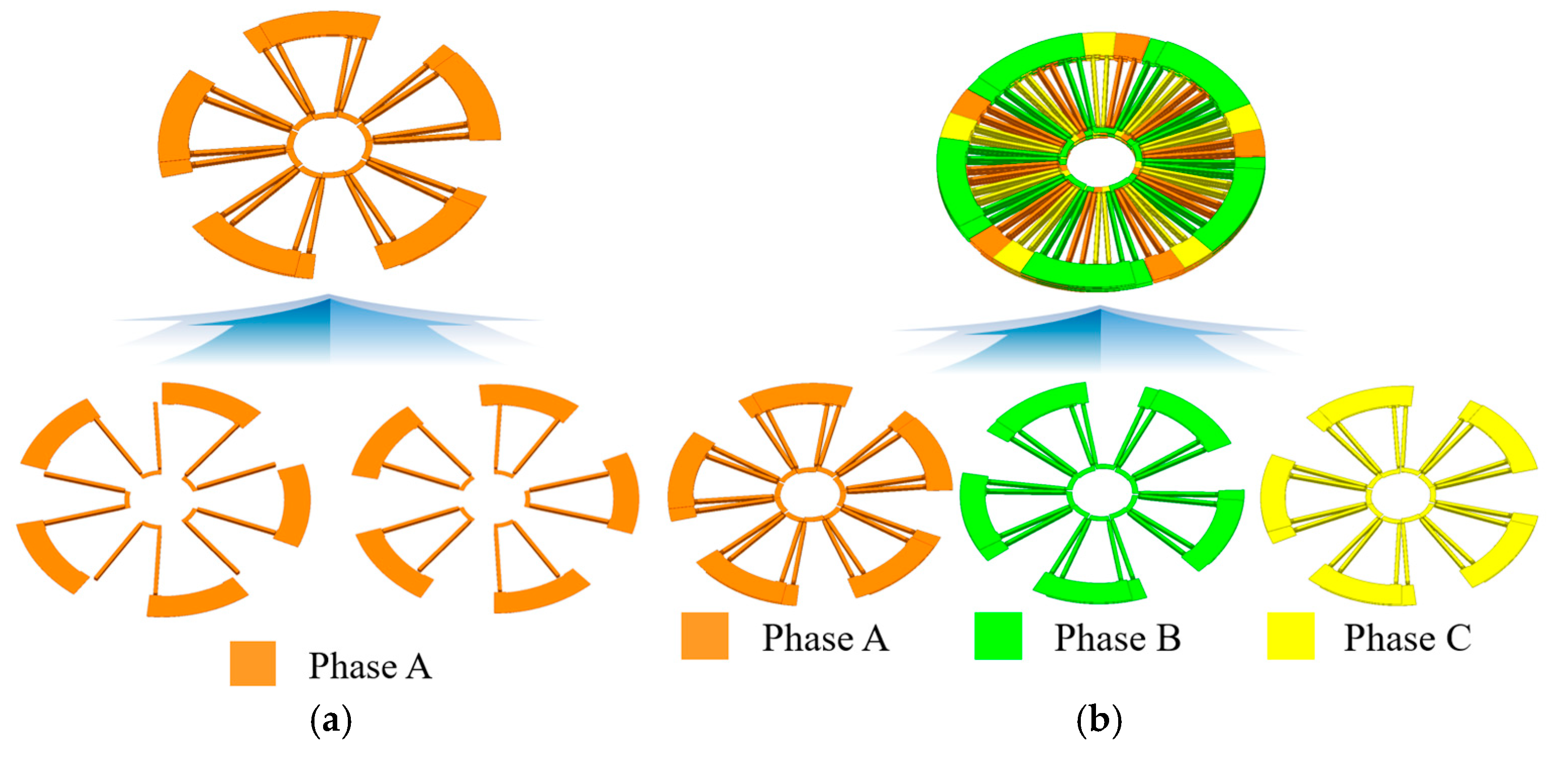
Figure 2a shows the single-phase PCB substrate, whereas Figure 2b shows the three-phase PCB substrate. The stator integrates all three phases on a single board, adopting a distributed winding layout with a pole-to-slot ratio of 1:3 [11]. Six copper layers are stacked to obtain two turns per slot for each phase, and the upper and lower layers are electrically linked through vias, guaranteeing uninterrupted current flow in the multilayer PCB [11]. As illustrated in Figure 2a, each phase appears to split into two separate conductor shapes, but these traces are connected through end-turns to form one continuous current path; the two shapes are, therefore, segments of the same phase rather than independent phases. Figure 2b consequently represents a complete three-phase, two-turn (3Φ 2T) winding configuration. Compared with conventional winding techniques, this PCB stator greatly simplifies manufacturing and is well suited to scalable mass production [12,20]. The design is especially advantageous for ultra-compact precision-actuator applications, where severe space constraints demand a thin, low-profile structure that still meets strict packaging requirements [3].
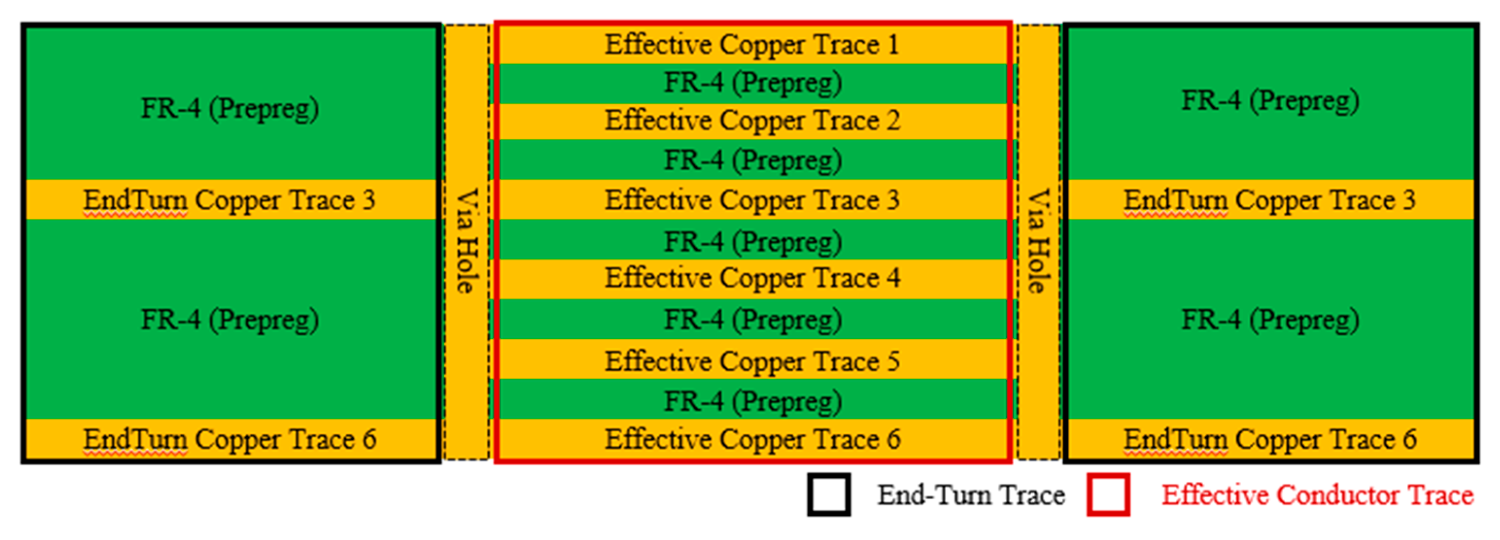
Figure 3 presents a cross-sectional view of the effective copper traces interconnected by via holes. The effective copper trace serves as the primary current-carrying path that directly contributes to torque generation. The effective traces for each phase are distributed across different PCB layers and electrically connected through vias to form a closed-loop circuit. These traces function as active conductors that interact magnetically with the rotor to deliver driving force.
Figure 4 shows the cross-section of the PCB winding layers. The end-turn traces provide return paths between effective copper traces within the same phase, and, positioned along the inner and outer boundaries of the PCB stator, the current begins at the inner end-turns (Layers 3 and 6), passes sequentially through each layer via the vias, and exits through the outer end-turns [11]. Although the end-turn traces themselves do not directly contribute to torque generation, they are essential for maintaining current continuity and circuit completeness [11]. Consequently, the structure consists of six parallel effective copper traces and two parallel end-turns on the inner and outer sides, establishing a stable two-turn current loop per phase. This parallel conductor arrangement lowers both resistance and copper loss, thereby enhancing overall efficiency [12].
The conductor resistance R is defined by Equation (1):
R = ρ L A
where ρ is the electrical resistivity, L is the current-path length, and A is the conductor cross-sectional area.
A T o t a l = N · A
When the number of parallel conductors is N, the total effective cross-sectional area increases as shown in (2), which directly leads to a reduction in the overall conductor resistance.
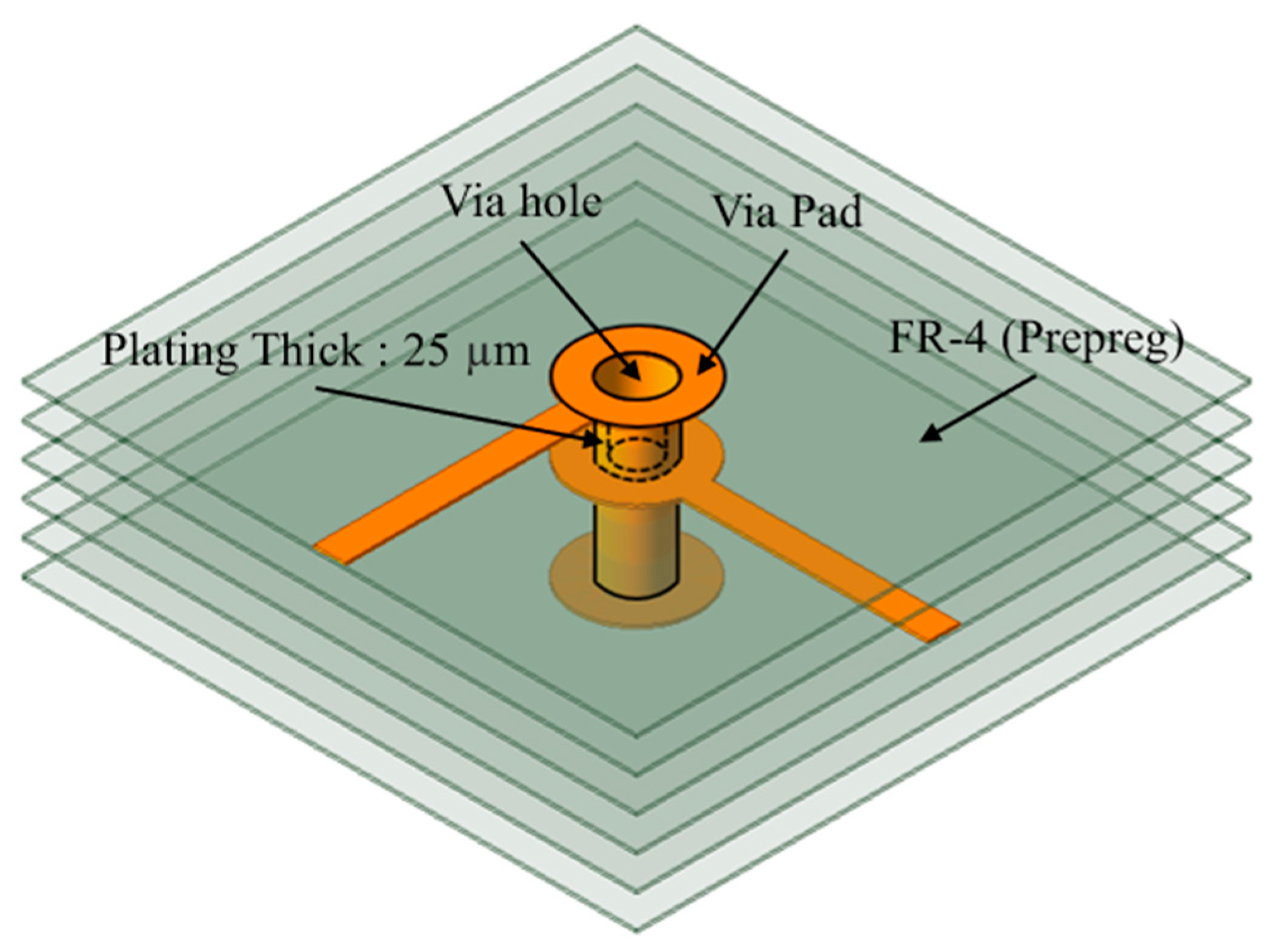
Figure 5 presents a three-dimensional exploded view of the plated via structure in the multilayer PCB stator. The inner wall of each drilled via is coated with a 25 µm copper layer, forming a cylindrical conductor [11]. Via pads on every layer act as bonding sites for the plating, providing dependable electrical connections to the upper- and lower-layer copper traces, while multiple FR-4 prepreg layers insulate adjacent copper sheets and preserve mechanical rigidity [11]. These vias link the upper and lower conductor traces, completing the current path across the six-layer PCB stack.
Effective conductor traces constitute the primary copper paths that carry current and generate torque; traces distributed across different layers are electrically interconnected through the vias to produce a single closed circuit with two turns per phase [11]. End-turn traces offer return paths within each phase, running between the inner (Layers 3 and 6) and outer end-turns and positioned along the stator boundary to maintain continuity of the inter-layer conductor network [11]. Fabricated with the standard 25 µm plating thickness, the vias align precisely with the pads of both effective and end-turn traces, thereby reducing electrical resistance and mitigating current crowding in the multilayer structure [16,17]; this ensures stable, well-distributed current paths even under high current density conditions [17].
The integrated architecture enables straightforward manufacturing while preserving an ultra-thin, lightweight form factor [12], delivering high electromagnetic performance and electrical reliability for space-constrained applications such as compact precision actuators [3].

2.3. Distributed Winding End-Turn Structure of the PCB Stator

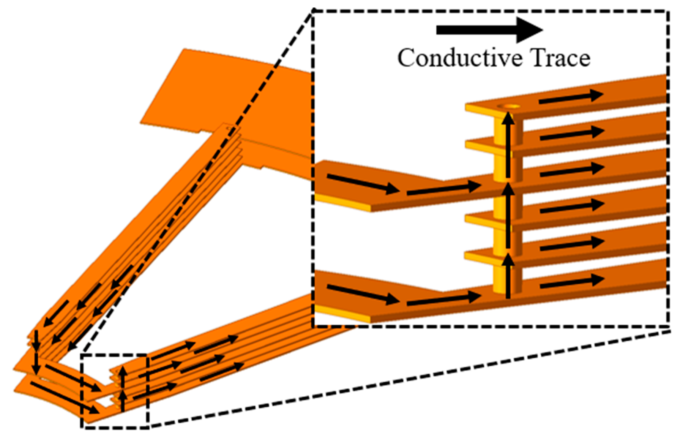
Figure 6 shows a three-dimensional enlarged view of the plated via network in the three-phase, two-turn PCB stator. Black arrows mark the current direction along each layer’s effective trace, and yellow columns depict inter-layer current flow through the vias. The stator integrates three phases with two dedicated end-turn layers per phase; this separation minimizes inter-phase interference and physically isolates each phase’s current path [11]. The total number of end-turn layers is determined by the turns per slot and the number of parallel PCB layers, which together close the current loop [11]. The parallel layer arrangement was tuned within the feasible design range to optimize end-turn placement, yielding a stable current distribution across all traces. As Figure 6 illustrates, the stator employs a distributed winding strategy that exploits the end-turn regions, providing magnetic force balancing and current distribution benefits comparable to those of conventional slotted distributed windings—even in a slotless structure [6]. End-turns interconnect the effective traces of each phase through vias, so current flows in a distributed manner across the parallel conductors, lowering current density and conductor resistance and thereby reducing copper loss [15]. Finally, the via-based inter-layer connections keep current path lengths among the effective traces precisely aligned, contributing to balanced torque generation across all three phases [11].

3. Multi-Via Design of the PCB Stator

3.1. Limitations of Conventional Single-Via Structures

Figure 7 shows the current density distribution concentrated inside the via of the conventional single-via model. The simulation results indicate peak current densities exceeding 5 × 10⁵ A mm−2 along the via wall (red region), whereas the surrounding copper traces exhibit much lower values (cyan–green regions). Although a single via links the inter-layer current paths in a multilayer PCB, the actuator-grade AFPM PCB stator investigated here must carry 12.37 A to deliver its rated output of 114.67 W; consequently, a single-via configuration cannot distribute the current effectively. Under the limited copper plating thickness of 25 µm, local heating and thermal saturation risks increase, the effective cross-sectional area for current flow is restricted, phase resistance rises, and both power loss and efficiency degradation occur [17]. Over prolonged operation, such thermal and electrical concentration can weaken via reliability and elevate the likelihood of failure [17].
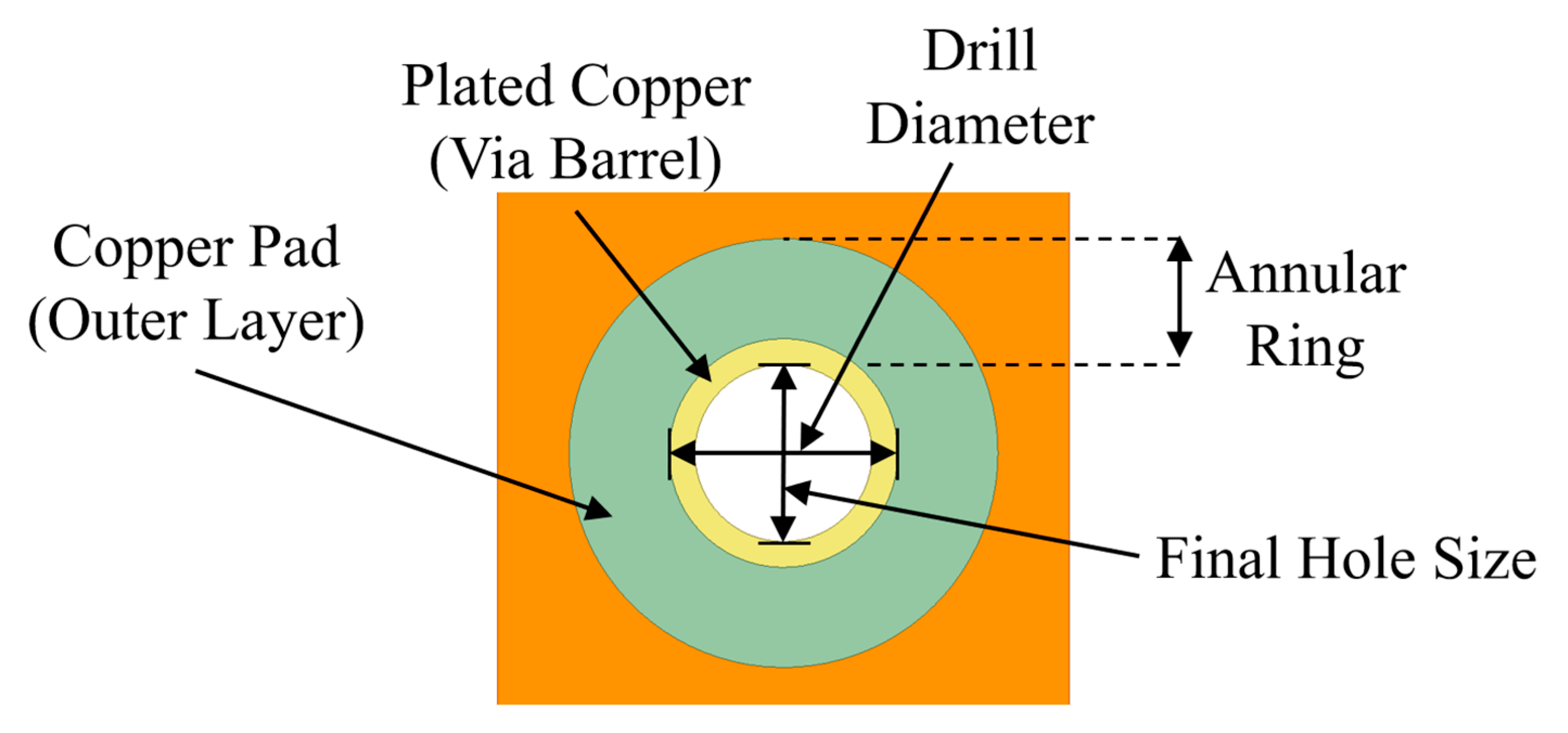
Figure 8 illustrates the cross-sectional layout of the via hole, plated copper barrel, and surrounding pad area. A PCB via is a cylindrical conductor formed by plating the inner wall of a drilled hole; its conductive cross-section is determined by the plating thickness and the drill diameter. The effective current-carrying area of the via is represented by an annular cross-section, as expressed in Equation (3).
A V i a = π r 2 r t 2 = π ( 2 r t t 2 )
where r is the radius of the drilled hole, and t is the plating thickness of the via wall.
t   r
In most cases, as shown in Equation (4), the expression can be approximated and simplified as in Equation (5).
A V i a 2 π r t
Accordingly, the electrical resistance of the via is given by the general conductor-resistance formula, as shown in Equation (6).
R V i a = ρ · l A V i a ρ · l 2 π r t
where ρ is the electrical resistivity of copper, and l is the PCB thickness (i.e., the via length). Equation (6) shows that the via resistance R V i a decreases as the via radius r increases. Nevertheless, from a practical design standpoint, arbitrarily enlarging the via radius is undesirable for three reasons. First, because the conductive copper is only a thin plated layer of thickness t, increasing the drill radius reduces the proportion of conductive plating in the via’s cross-sectional area [17]. Second, an excessively large via diameter restricts routing space on the PCB and undermines the mechanical and thermal robustness of the current path [16]. Third, since the plating thickness t is fixed by process constraints, increasing the radius alone does not meaningfully improve current-carrying capacity [17].
π ( 2 r t t 2 )
The effective cross-sectional area of a via is given by Equation (7) when the plating thickness t is much smaller than the radius r , the area can be approximated as 2 π r t . Accordingly, the via resistance is defined by Equation (8) and, in theory, decreases as the via radius increases.
R = ρ l / ( 2 π r t )
However, as the drill diameter grows, the proportion of the actual copper conductive layer within the cross-section diminishes, indicating that enlarging a single via’s diameter is not an effective way to reduce resistance.

3.2. Multi-Via Structure

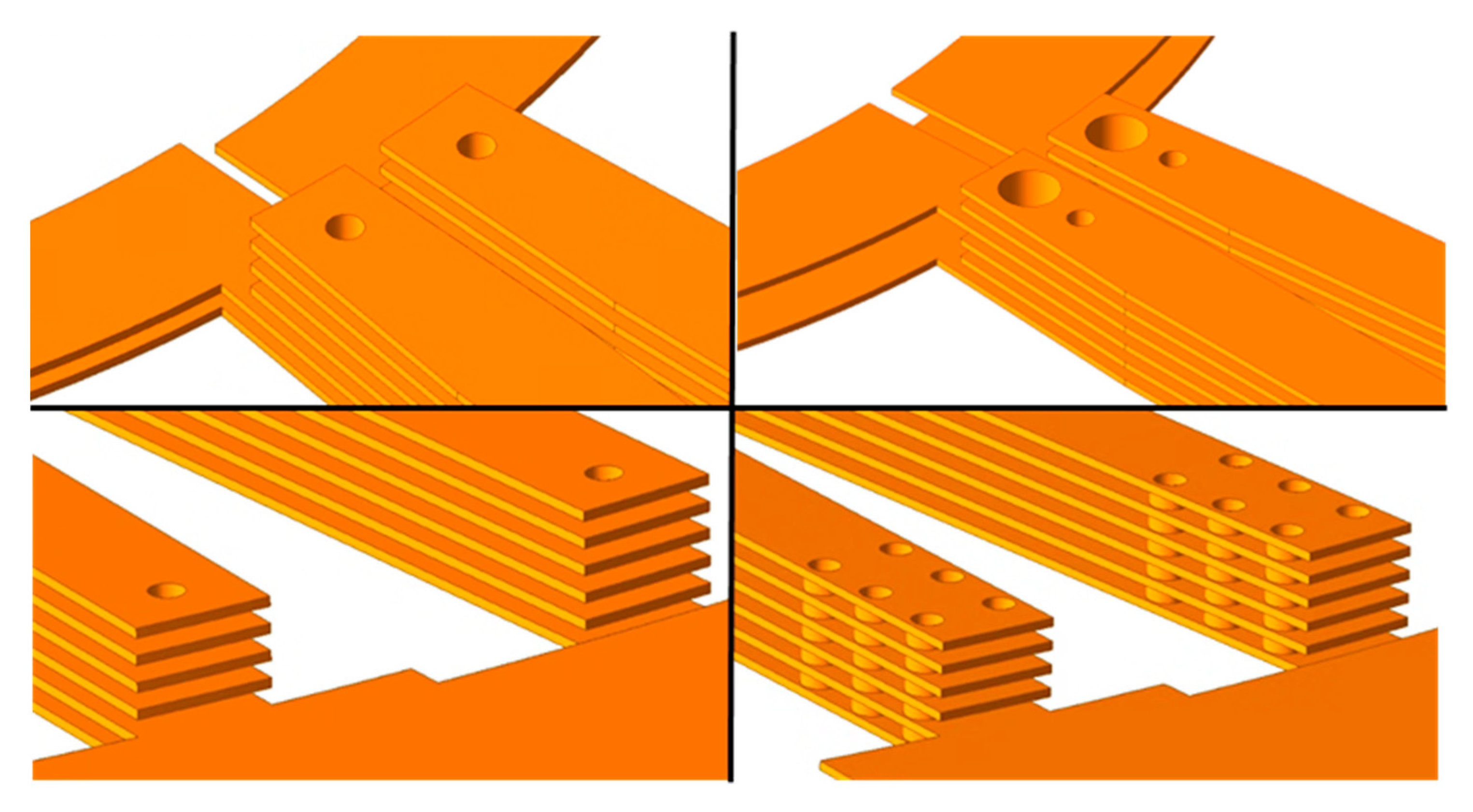
Figure 9 compares the single-via and multi-via configurations in the inner and outer end-turn regions. The single-via configuration (left) employs one plated through hole for each layer-to-layer connection, whereas the multi-via configuration (right) incorporates multiple parallel vias to reduce local current crowding and lower effective resistance. The top images show enlarged views of the inner end-turn region, while the bottom images illustrate the outer end-turn region. All conductor layers are implemented on a multilayer PCB with 2 oz copper plating. In the single-via structure, each effective conductor layer is interconnected by only one via, producing several disadvantages. First, the current is forced through a narrow path, resulting in a high current density within the via [17]. Second, the limited cross-sectional area raises electrical resistance and, consequently, copper loss [17]. Third, the associated thermal concentration can degrade long-term reliability [16]. Because the via lies directly on the main current path, its resistance adds to the total equivalent resistance, and the elevated local current density concentrates heat in the via, accelerating aging and reducing durability [16,17].
Therefore, a multi-via design must do more than simply increase the via count; the vias must be placed strategically along the current path to minimize loss and provide an optimized, reliable layout [16]. To systematically evaluate and optimize the multi-via design, this study employed a step-by-step procedure. First, a two-turn PCB stator consisting of two 6-layer boards was chosen as the baseline configuration, considering the trade-off between back-EMF requirements and AC loss. This selection reflects a limitation inherent to the chosen motor topology, which may restrict the direct applicability of the results to other winding patterns. Step 1: The single-via structure was analyzed by gradually varying the via diameter to establish reference trends in phase resistance and current density. Step 2: Inline multi-via structures were introduced, and the effects of sequential via placement at the inner and outer end-turns were examined. Step 3: Grid multi-via structures were applied, distributing multiple smaller vias across the conductor segment to improve current sharing and reduce resistance. Step 4: Finally, the inline and grid configurations were quantitatively compared, and the optimal layout was identified by balancing current distribution effectiveness with conductor area utilization.

3.3. Inline-Type and Grid-Multi-Via Structures

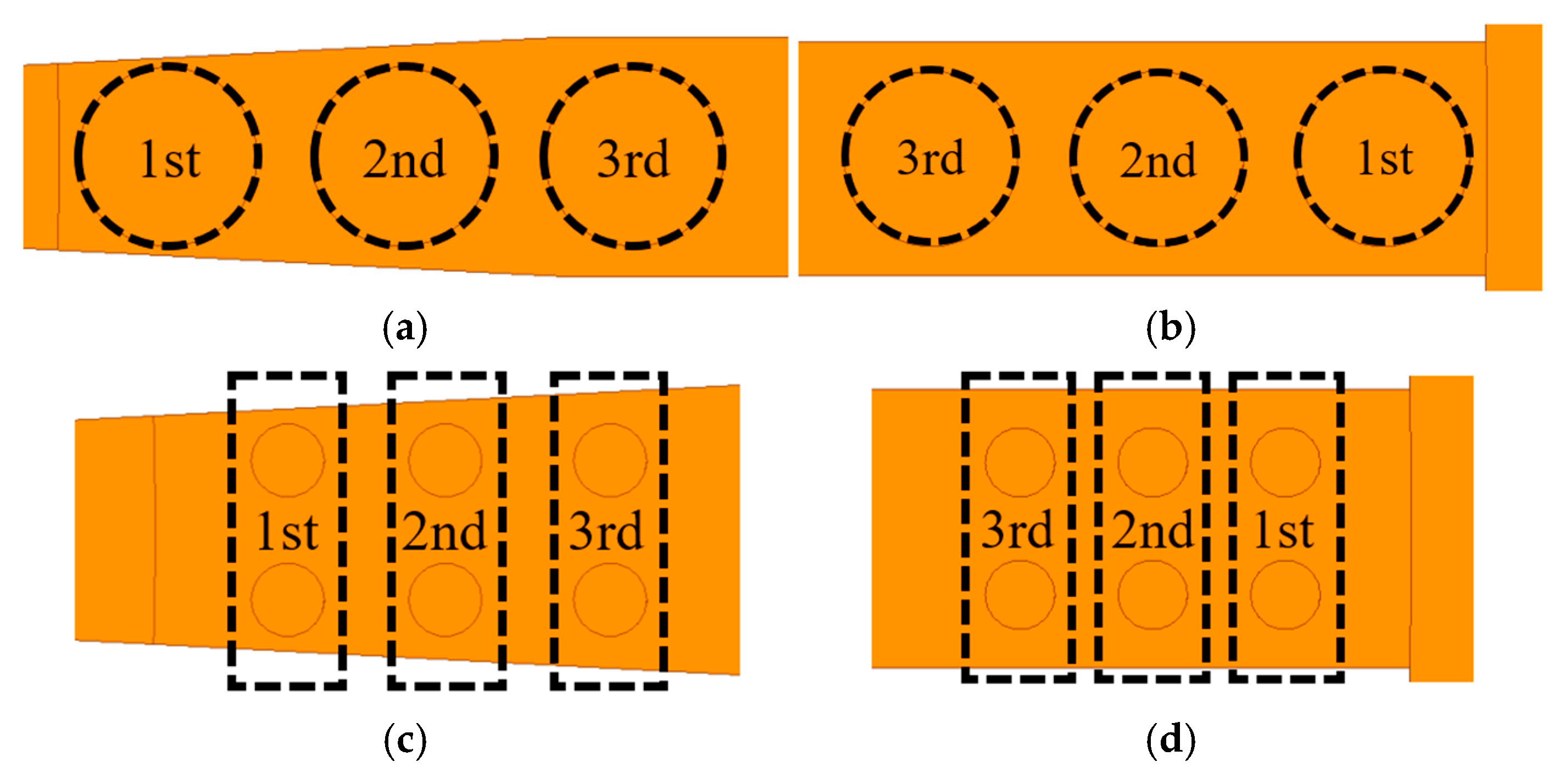
The top row shows the inline configuration, while the bottom row presents the grid configuration. (a) and (b) display the inner and outer end-turns of the inline design, where vias are sequentially inserted from the conductor tip. (c) and (d) illustrate the grid design, in which multiple parallel vias are distributed throughout the conductor segment to equalize current density. Compared with the inline configuration, the grid structure more effectively mitigates current crowding, reduces resistance, and enhances thermal dissipation, while maintaining full compatibility with standard PCB fabrication processes.
Figure 10a shows the inline multi-via structure at the inner end-turn. Vias are arranged in a single row and inserted in the sequence 1 → 2 → 3, starting from the terminal end of the conductor. This layout directs incoming current from the inner side through the conductor tip first, mitigating localized current concentration and reducing heat generation.
Figure 10b presents the inline multi-via structure at the outer end-turn. Although the physical order is 3 → 2 → 1, the insertion sequence remains 1 → 2 → 3. This arrangement distributes current entering from the outer side toward the conductor tip first, optimizing the current path and enhancing both electrical and thermal performance.
Figure 10c illustrates the grid multi-via structure at the inner end-turn. Each row consists of a pair of vertical vias, added sequentially in the order 3 → 2 → 1. Consequently, two, four, and six vias are distributed across the conductor segment, effectively reducing current density and electrical resistance.
Figure 10d shows the grid multi-via structure at the outer end-turn. While the physical arrangement is 3 → 2 → 1, the insertion sequence again follows 1 → 2 → 3. Because current enters from the outer side, prioritizing via connections near the conductor tip minimizes thermal loss and electrical resistance.
In the two-turn conductor pattern used in this study, the grid multi-via approach offers superior electrical performance compared with the inline configuration. In inline designs, if space is insufficient for multiple vias at the same location, enlarging the via diameter can lower internal current density; however, the resulting larger plated area occupies more of the effective conductor, reducing copper cross-section and increasing phase resistance. When adequate spacing between conductors is available—as in the present two-turn layout, the grid method, which distributes multiple small vias, more effectively mitigates current density and lowers resistance. Considering factors such as number of turns, conductor width, via arrangement, parallel current paths, and manufacturability, the grid multi-via configuration is optimal for a two-turn PCB stator. This design provides superior resistance reduction and thermal dissipation performance while remaining compatible with standard PCB fabrication processes.

3.4. Simulation Conditions

In this study, the rotor and stator structures were kept identical; only the via configuration was varied to compare and analyze electrical characteristics such as phase resistance and current density. The analysis conditions were as follows. First, for the single-via structure, the via diameter was gradually increased, and the resulting changes in phase resistance and current density distribution were evaluated. This analysis considered both the reduction in current density due to the enlarged via diameter and the opposing effect of decreased effective conductor area—caused by the enlarged plated via region within the same conductor width—on resistance behavior. Second, for the multi-via structures, two configurations were investigated: inline multi-via and grid multi-via. For both configurations, the via diameter was incrementally increased within the same effective conductor width. The current distribution effect and conductor loss characteristics of each structure were then compared. Through this evaluation, an electrical performance optimization strategy was established by balancing the benefit of an increased plated via area against the reduction in effective conductor cross-section.
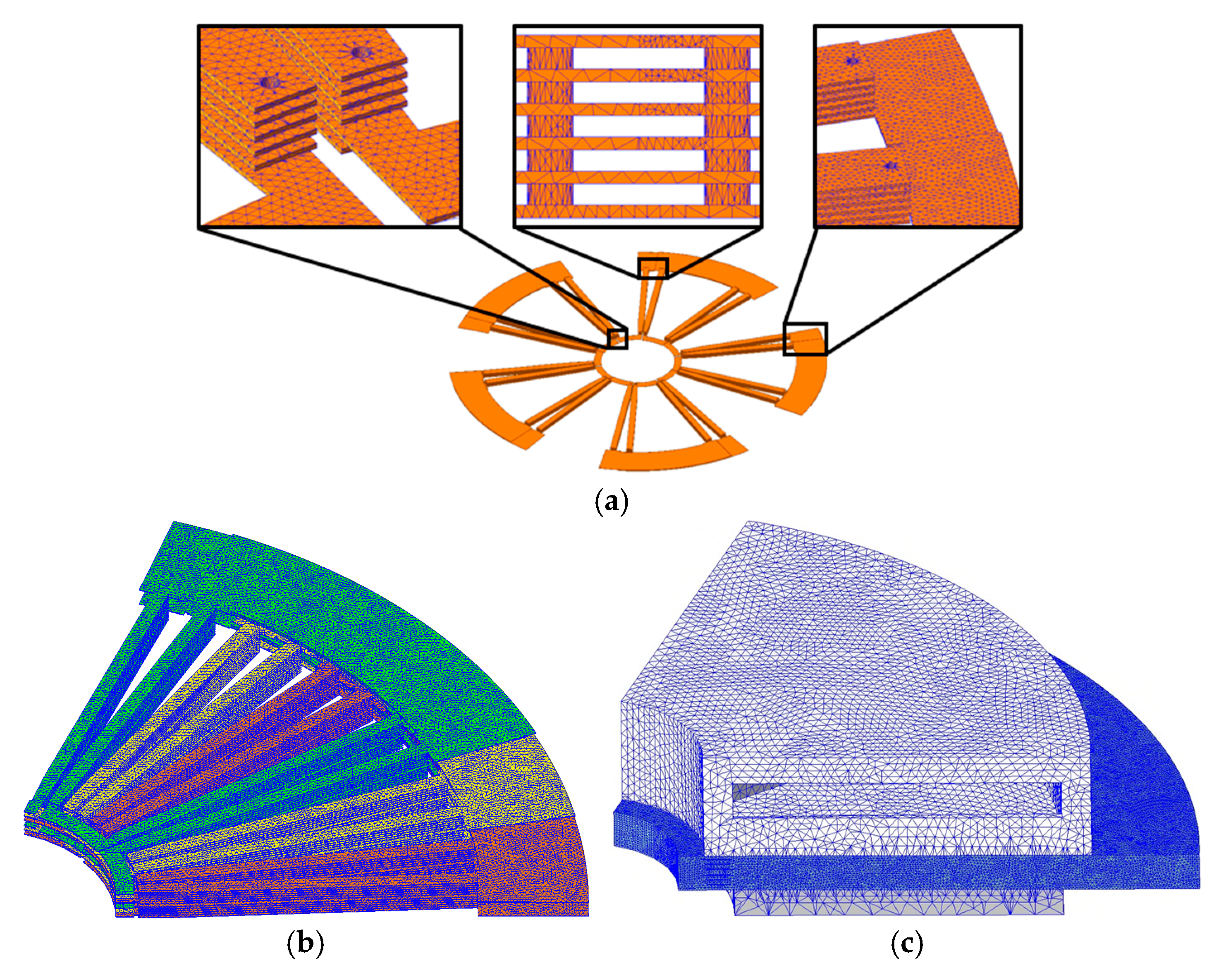
In addition, the finite-element simulations were performed using ANSYS Maxwell 3D, Release 2025 R2 with the Eddy Current Solver for resistance and current density evaluation. Adaptive meshing with a minimum element size of 200 μm was applied to ensure accuracy, and representative mesh distributions are shown in Figure 11. Specifically, the mesh applied to the PCB stator and via regions for eddy current analysis is presented in Figure 11a, while Figure 11b,c illustrates the mesh discretization of the multilayer PCB circuit and the refined airgap/airband region used in transient electromagnetic simulations for torque and dynamic field evaluation. No special boundary conditions were applied beyond the default solver settings.

4. FEM Methodology and Performance Evaluation

4.1. Analysis Items

The stator employs a parallel layer configuration with two vias—inner and outer—allocated to each slot. These vias electrically connect the upper and lower effective conductors, enabling current distribution across layers. In this study, the diameters of the inner and outer vias were varied independently to evaluate their effects on phase resistance and current density, with the aim of identifying the optimal combination of via diameter and placement. The analysis began with the single-via structure, uniformly increasing both inner and outer via diameters in successive FEM simulations. Building on these results, inline multi-via (IM-via) and grid multi-via (GM-via) configurations were then applied to the inner and outer regions. After determining the inner via condition that minimized phase resistance, the same procedure was applied to the outer via to obtain the overall optimal layout. This step-by-step approach allowed separate sensitivity studies of phase resistance and current density with respect to via diameter and layout, enabling a quantitative optimization that balances current distribution effectiveness against conductor area utilization.

4.2. FEM-Based Performance Analysis

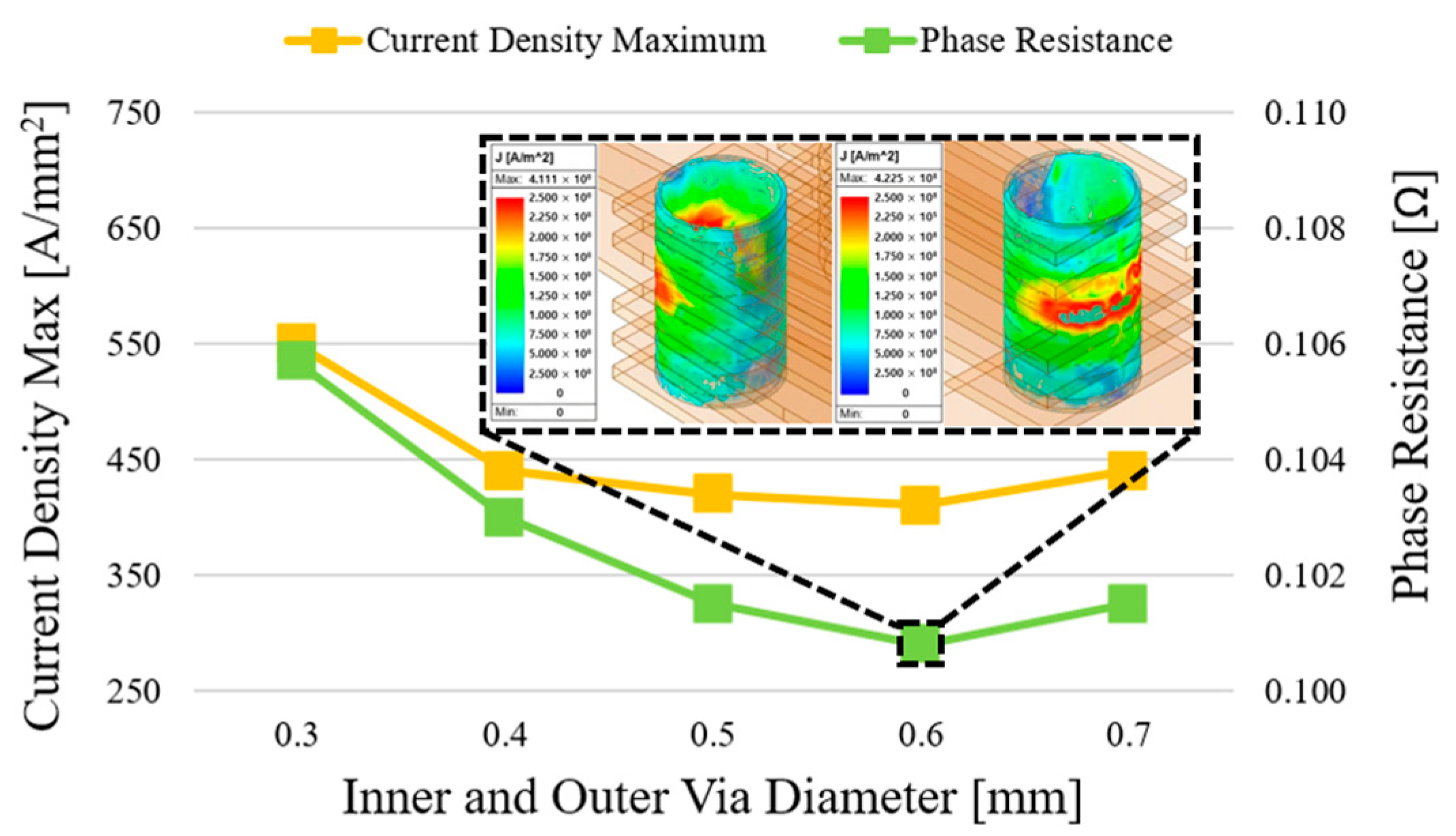
Figure 12 shows that, in the single-via configuration, a via diameter of 0.60 mm produces the lowest values—0.1008 Ω in phase resistance and 425 A/mm2 in peak current density—corresponding to reductions of approximately 4.63% and 22.73%, respectively, relative to the 0.30 mm baseline. These improvements stem from the enlarged effective current path and enhanced current spreading that accompany an increase in via diameter, which mitigate loss and local heating caused by current crowding. Once the via diameter surpasses this optimal value, however, both phase resistance and peak current density rise again because the larger via removes copper from the effective conductor, narrowing the remaining conductive path. Simply enlarging a single via, therefore, does not always reduce resistance; beyond a certain point, it can have the opposite effect. Optimal via design must balance current spreading effectiveness against retention of a sufficient copper cross-section.
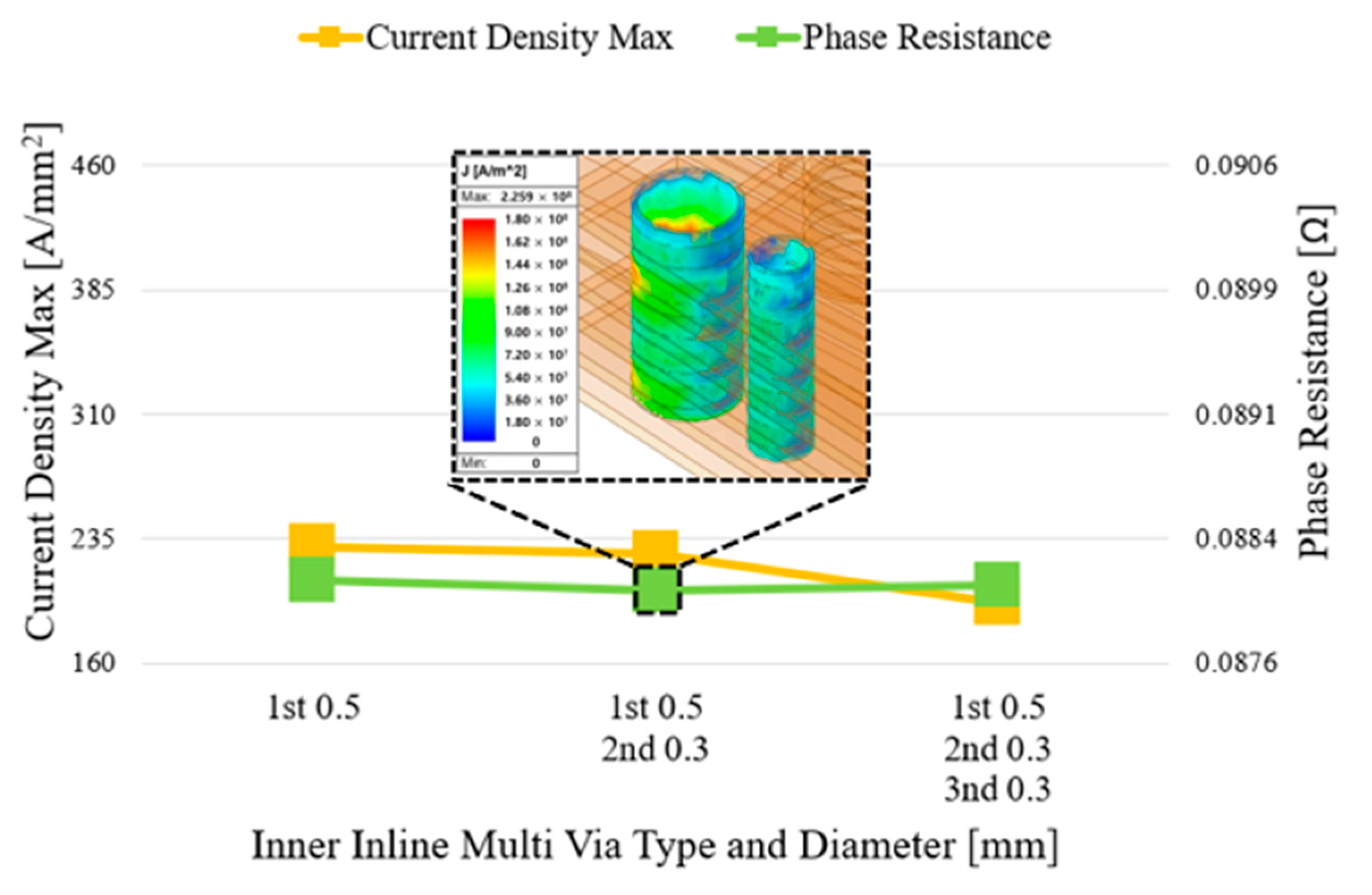
Based on the preceding single-via analysis, Figure 13 evaluates phase resistance and current density characteristics by incrementally applying the IM-via structure to the inner via while keeping the outer via fixed at the baseline diameter of 0.30 mm. For each via position (1st, 2nd, and 3rd), the diameter was varied from 0.30 mm to 0.70 mm, and the resulting phase resistance values were quantitatively compared. The lowest phase resistance occurs with a 0.50 mm diameter for the 1st via and 0.30 mm for the 2nd via, identifying this pair as the optimal IM-via configuration. Adding a 3rd via provides only marginal resistance reduction, and in some cases even increases resistance, because additional vias reduce the effective conductor area and distort the current path, leading to local crowding and extra loss. The graph in Figure 13 plots the minimum phase resistance value obtained for every via-diameter combination (0.30–0.70 mm) at the 1st, 2nd, and 3rd positions, making the optimal design point easy to identify. In summary, for the IM-via structure, the 1st-via 0.50 mm and 2nd-via 0.30 mm combination is optimal. These results confirm that precise coordination of via position and diameter, rather than simply increasing the via count, is essential for improving electrical performance.
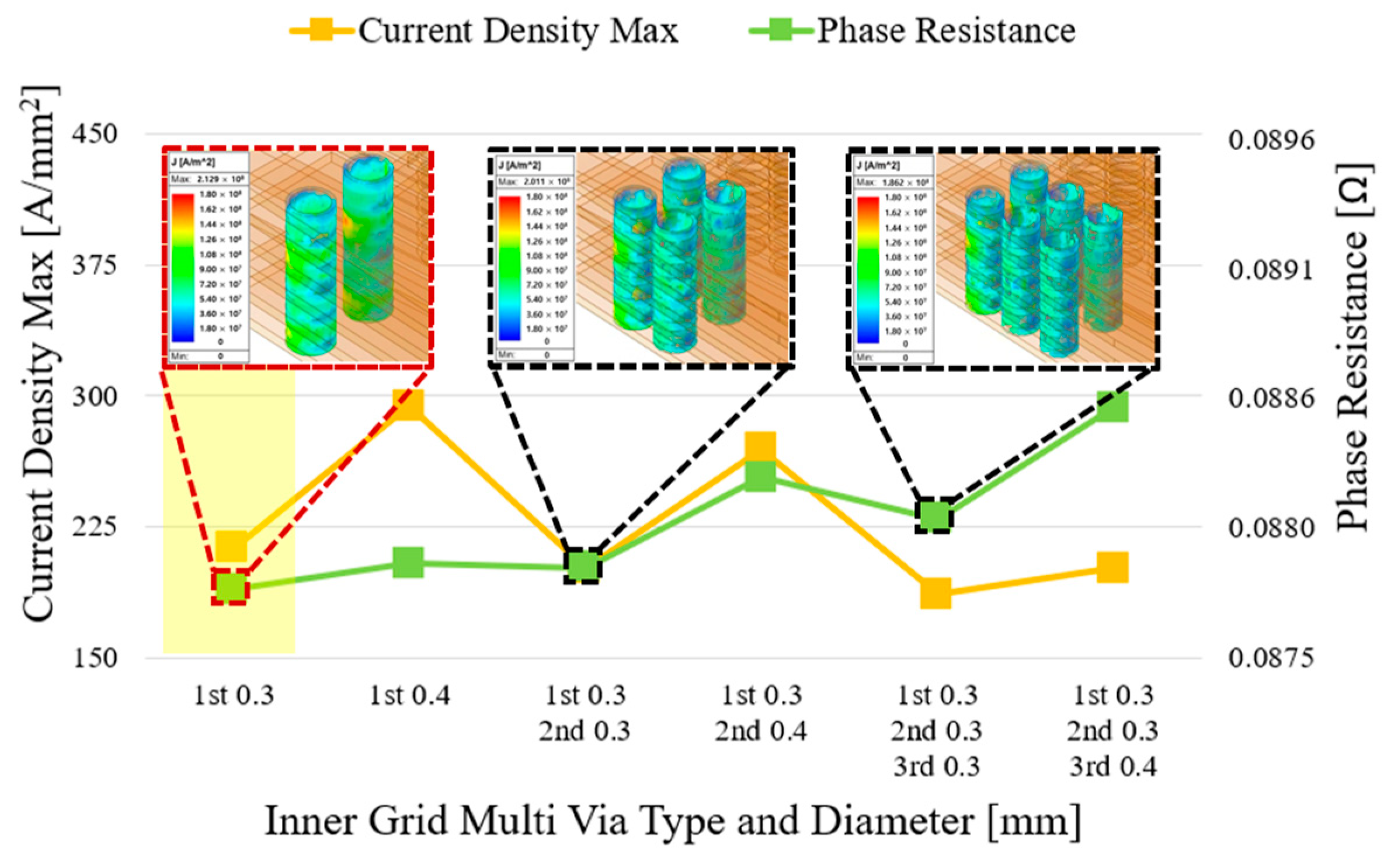
Figure 13, under the same conditions as the IM-via analysis in Figure 12, evaluates phase resistance and current density characteristics by fixing the outer via at the baseline diameter of 0.30 mm and applying a GM-via configuration to the inner via. In the GM-via scheme, two vias are placed in parallel across the conductor width at each position. Considering space constraints and conductor interference, the via diameter was varied from 0.30 mm to 0.40 mm. The analysis proceeded in three stages: two vias at the 1st position, four vias at the 1st + 2nd positions, and six vias at the 1st + 2nd + 3rd positions. Phase resistance and current density performance were compared for every combination.
The best result was obtained with two 0.30 mm diameter vias at the 1st position, yielding a minimum phase resistance of 0.0878 Ω. Relative to the baseline model (inner and outer vias both 0.30 mm, phase resistance 0.1057 Ω), this represents a 16.96% reduction. The peak current density at the inner via also decreased from 410 A/mm2 to 212 A/mm2, a 48.29% reduction. Adding vias at the 2nd and 3rd positions, thereby increasing the via count, often raised phase resistance. Excessive vias reduce the effective conductor area and distribute current inefficiently, which degrades electrical performance. In the GM-via layout, horizontally paired vias further increase copper area loss and conductor interference as diameter grows, raising resistance.
Figure 14 shows the lowest phase resistance value for each combination obtained from FEM simulations over the 0.30–0.40 mm diameter range at the 1st, 2nd, and 3rd stages. Overall, the GM-via scheme achieves lower resistance than the IM-via approach, and the simplest configuration (two 0.30 mm vias at the 1st position) proves most effective. This option is also the easiest to manufacture and confirms that adding more vias does not necessarily improve performance.
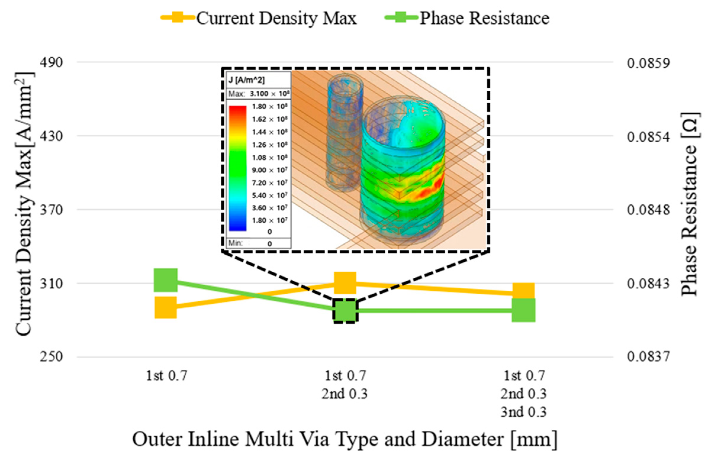
Figure 15 builds on Figure 14, in which the inner via uses the GM-via scheme, and the configuration with two 0.30 mm vias at the 1st position proves optimal. With that condition fixed, the present stage applies the IM-via structure to the outer via to evaluate additional phase resistance and current density characteristics. The arrangement is the same as before, except that the outer vias are stacked inward from the stator edge in the order 1st → 2nd → 3rd. For each position, the via diameter is varied stepwise from 0.30 mm to 0.70 mm, and the resulting performance differences attributable to current spreading are quantified.
The lowest phase resistance is obtained with a 0.70 mm via at the 1st position and a 0.30 mm via at the 2nd position, indicating that a large-diameter via at the outermost location secures the main current path, while smaller vias in subsequent positions provide auxiliary current dispersion. Adding a 3rd via yields no significant additional reduction, offering limited benefit compared with the added design complexity.
Figure 15 plots the minimum phase resistance value for every position–diameter combination obtained from the FEM simulations, confirming that strategic selection of via positions and diameters, rather than merely increasing the via count, is decisive for improving electrical performance.
Figure 16 summarizes the FEM results for all GM-via combinations at the 1st, 2nd, and 3rd positions, graphing the lowest phase resistance value obtained in each set. For the inner via, the GM-via arrangement identified in Figure 14—two 0.30 mm vias at the 1st position—gives the best electrical performance, yielding a phase resistance of 0.0878 Ω and a peak current density of 212 A/mm2. With this inner via condition fixed, the same GM-via scheme is applied to the outer via, and the resulting phase resistance and current-density characteristics are evaluated.
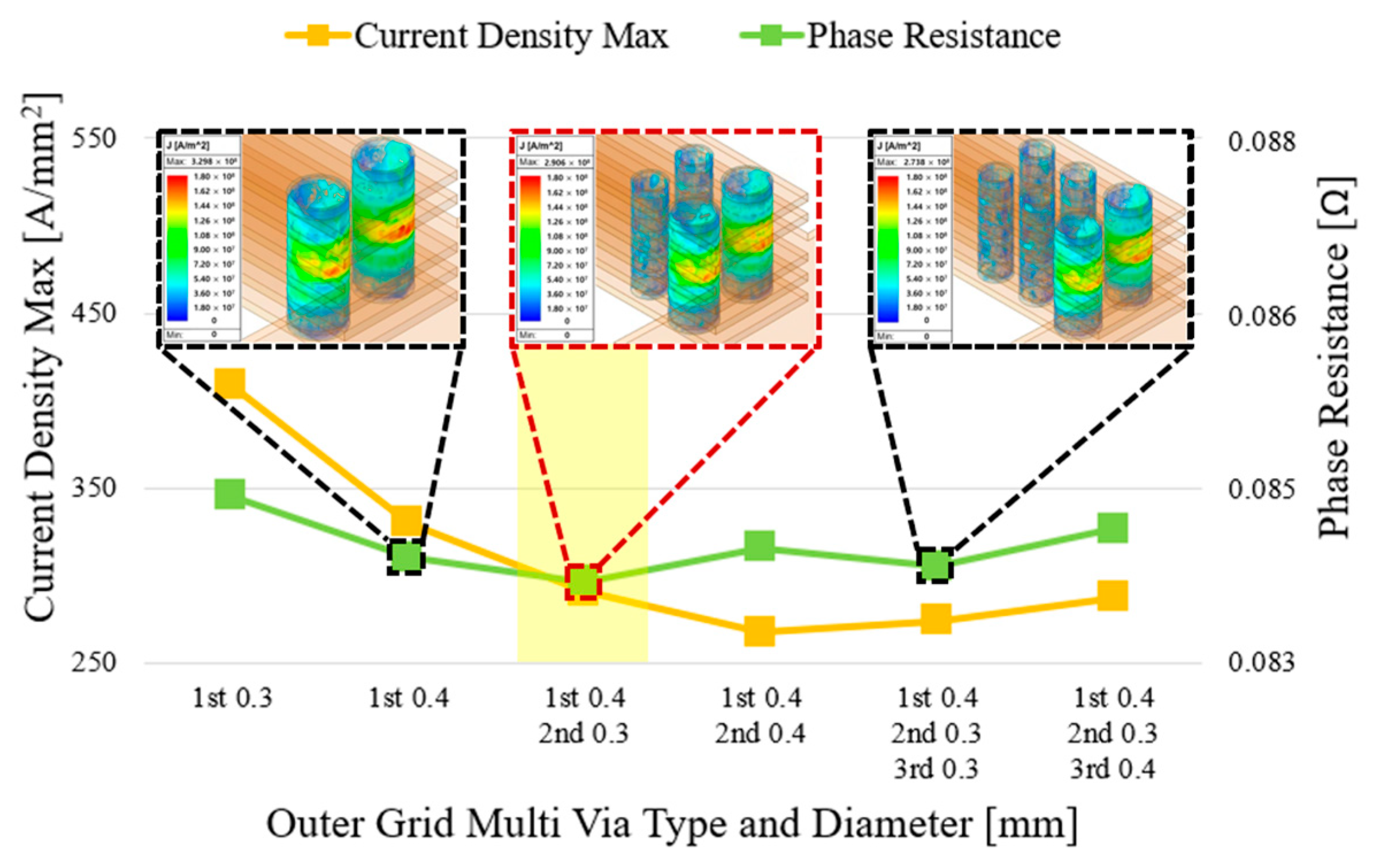
For the outer GM-via, two side-by-side vias are placed at each position (1st, 2nd, and 3rd) with diameters swept from 0.30 mm to 0.40 mm, resulting in two, four, and six total vias for the 1st, 1st + 2nd, and 1st + 2nd + 3rd stages, respectively. FEM analysis shows that a 0.40 mm via at the 1st position combined with a 0.30 mm via at the 2nd position (1st 0.4, 2nd 0.3) provides the best performance, with a phase resistance of 0.0837 Ω and a peak current density of 290 A/mm2. Relative to the optimal inner GM-via case with a single 0.30 mm outer via (phase resistance 0.0878 Ω), this configuration lowers phase resistance by 4.67%. Compared with the baseline single-via design (inner and outer vias both 0.30 mm, peak outer via current density 422 A/mm2), the peak current density decreases by 31.28%. Even against the optimal IM-via outer arrangement (1st 0.7 mm, 2nd 0.3 mm; phase resistance 0.0843 Ω, current density 310 A/mm2), the GM-via layout achieves lower phase resistance and current density. Overall, it reduces phase resistance by 20.76% relative to the single-via baseline.
These results confirm that the GM-via approach provides a more efficient current-distribution path for outer via design. Applying GM vias strategically to both inner and outer locations yields the greatest performance improvement over the single-via and IM-via schemes, demonstrating that precise selection of via position and diameter, rather than simply increasing via count or size, is essential for optimal PCB stator design.
According to the three-dimensional finite-element results in Table 3, the grid multi-via (GM-via) design evaluated under the same operating conditions as the baseline single-via model (identical back-EMF, rated speed of 3650 rpm, load torque of 0.3 Nm, line current of 12.57 A rms, and output power of 114.67 W) reduces the peak current density from 42.19 A·mm−2 to 33.45 A·mm−2 (≈20.7%) and lowers the phase resistance from 0.106 Ω to 0.083 Ω (≈21.7%). This resistance reduction directly decreases I2R losses, with copper loss falling from 50.08 W to 39.70 W (≈20.7%), which in turn raises overall efficiency from 66.72% to 71.01%, that is, +4.29 percentage points (≈6.4%). These results confirm that the GM-via layout equalizes current paths, mitigates localized current crowding, and effectively increases the usable conductor cross-section under identical mechanical specifications.
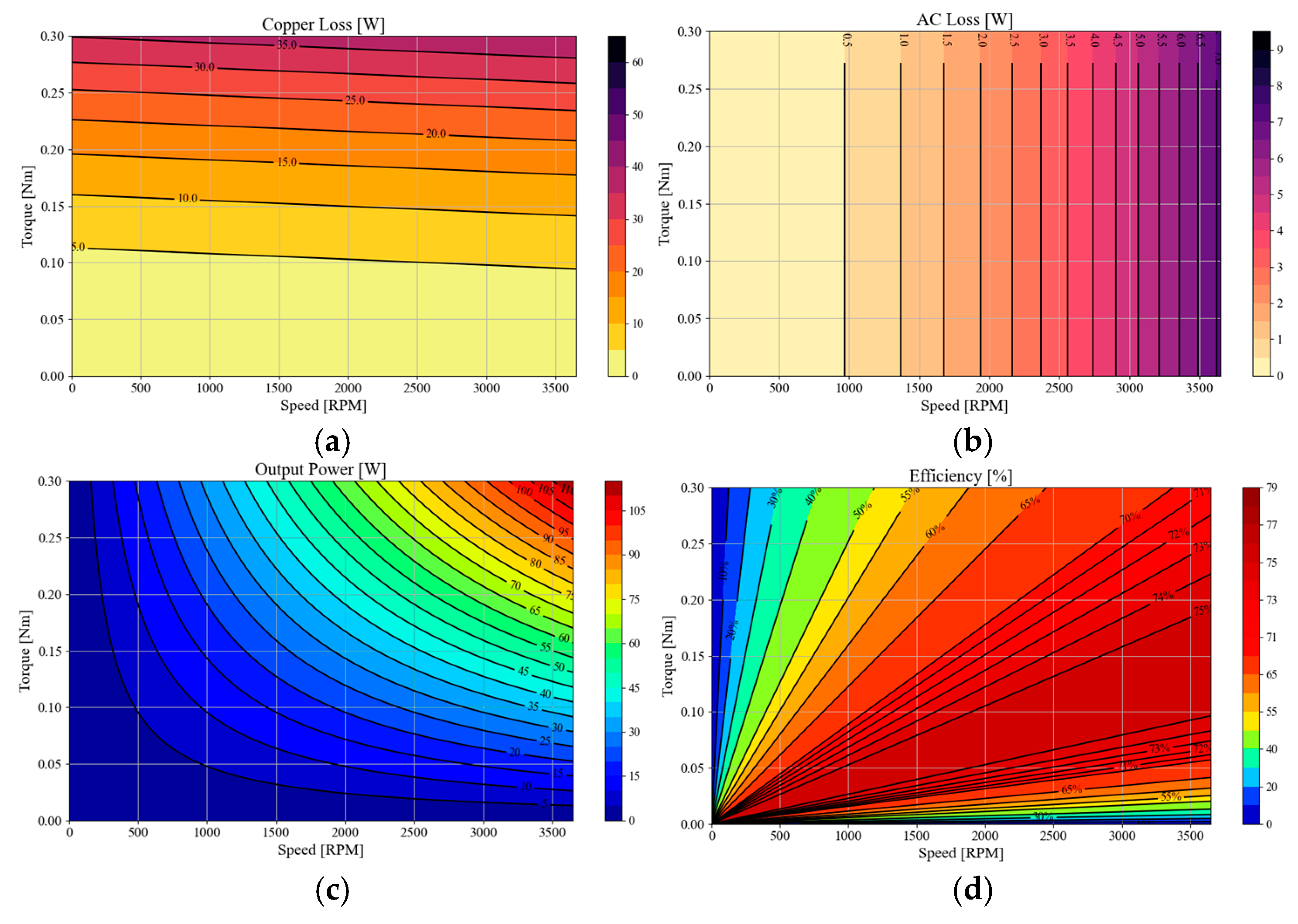
In Figure 17, (a) Copper loss, increasing approximately with the square of load current (torque), is ≈20% lower in the GM-via design at rated operation, consistent with the resistance reduction. (b) AC loss, dominated by speed (frequency-dependent effects), shows minor sensitivity to torque and peaks near the highest rpm. (c) Output power, following P o u t -Tω reaches 114.67 W at the rated point, indicating that loss reduction does not compromise deliverable power. (d) Efficiency, reflecting the combined influence of losses and output, exceeds 70% near the rated region, with a maximum of 71.01% compared to 66.72% for the single-via baseline.

5. Conclusions

This study presents an optimal design for a compact axial flux permanent magnet motor (AFPM) that employs an ultra-thin, high-density PCB stator. A multi-via configuration was introduced to reduce phase resistance and peak current density, thereby improving overall electrical performance. Step-by-step FEM analyses were carried out for both inline and grid multi-via schemes to determine the optimal via arrangement. Using the grid multi-via structure, phase resistance decreased from 0.106 Ω to 0.084 Ω (≈20.8%), and peak current density fell from 42.19 A/mm2 to 33.45 A/mm2 (≈20.7%) relative to the single-via baseline. Copper loss was reduced from 50.08 W to 39.7 W, while overall efficiency increased from 66.72% to 71.01%, with output power and other operating conditions held constant. These results demonstrate that carefully selecting via position and diameter, rather than simply increasing the via count, provides the best balance between design complexity and electrical performance. Unlike earlier PCB-stator motor studies, which lacked systematic optimization of via structures, this work offers a practical design methodology that simultaneously accounts for via diameter, placement, and the number of parallel layers. Real manufacturing constraints, such as minimum drill diameter and copper clearance limits, are also included, ensuring both practicality and reproducibility.

Author Contributions

Conceptualization and design, W.-H.K. (including study concept, critical revision, and final approval); methodology development and data curation, S.-B.J. (including experimental design, data management, drafting the initial manuscript, and approval of the final version); software development and resource provision, D.-H.C. (including technical implementation, critical review, and final accountability for the software components); validation and overall research oversight, Y.-H.S. (ensuring data integrity and accountability throughout the study); formal analysis and investigation, H.-S.H. (performing comprehensive data analysis, interpretation, and figure visualization); writing—original draft preparation, S.-B.J. (responsible for drafting the manuscript followed by critical revision by all authors); writing—review and editing, S.-B.J. and D.-H.C. (providing in-depth manuscript reviews, revisions, and final manuscript approval); visualization, Y.-H.S. and H.-S.H. (developing data visualizations, ensuring clarity in presentation); supervision and project management, W.-H.K. (overseeing the entire research process and endorsing the final submission). All authors have read and agreed to the published version of the manuscript.

Funding

This work was partly supported by the Korea Institute of Energy Technology Evaluation and Planning (KETEP) grant funded by the Korea government (MOTIE) (20214000000060, Department of Next Generation Energy System Convergence based on Techno-Economics-STEP) and in part by the Korea Institute of Energy Technology Evaluation and Planning (KETEP) grant funded by the Korea government (MOTIE) (RS-2024-00419152, Development of 5 kW industrial logistics electric platform technology).

Data Availability Statement

The original contributions presented in the study are included in the article; further inquiries can be directed to the corresponding author.

Conflicts of Interest

The authors declare no conflicts of interest.

References

  1. Hsieh, F.-S. Emerging Research Issues and Directions on MaaS, Sustainability and Shared Mobility in Smart Cities with Multi-Modal Transport Systems. Appl. Sci. 2025, 15, 5709. [Google Scholar] [CrossRef]
  2. Turoń, K.; Tóth, J. Innovations in Shared Mobility—Review of Scientific Works. Smart Cities 2023, 6, 1545–1559. [Google Scholar] [CrossRef]
  3. Mittal, V.; Lotwin, M.; Shah, R. A Review of Bio-Inspired Actuators and Their Potential for Adaptive Vehicle Control. Actuators 2025, 14, 303. [Google Scholar] [CrossRef]
  4. Yu, P.; Sun, Z.; Xu, H.; Ren, Y.; Tan, C. Design and Analysis of Brake-by-Wire Unit Based on Direct Drive Pump–Valve Cooperative. Actuators 2023, 12, 360. [Google Scholar] [CrossRef]
  5. Gong, X.; Qian, L.; Ge, W.; Wang, L. Research on the Anti-Disturbance Control Method of Brake-by-Wire Unit for Electric Vehicles. World Electr. Veh. J. 2019, 10, 44. [Google Scholar] [CrossRef]
  6. Hao, Z.; Ma, Y.; Wang, P.; Luo, G.; Chen, Y. A Review of Axial-Flux Permanent-Magnet Motors: Topological Structures, Design, Optimization and Control Techniques. Machines 2022, 10, 1178. [Google Scholar] [CrossRef]
  7. Zhao, X.-K.; Zou, X.-P.; Guo, Q.-C.; Zhu, L.-K. Axial Flux Permanent Magnet Synchronous Motor Cogging Torque Calculation Method Based on Harmonic Screening. Energies 2025, 18, 3779. [Google Scholar] [CrossRef]
  8. Liu, W.; Yang, J.; Pei, L.; Rafiei, M.; Yang, Y.; Wang, Y.; Cui, J.; Guo, Y.; Zhang, B. Structural Optimization and Electromagnetic Performance Research of Axial Magnetic Field Tidal Current Generators. Energies 2025, 18, 2520. [Google Scholar] [CrossRef]
  9. Gao, P.; Gu, Y.; Wang, X. The Design of a Permanent Magnet In-Wheel Motor with Dual-Stator and Dual-Field-Excitation Used in Electric Vehicles. Energies 2018, 11, 424. [Google Scholar] [CrossRef]
  10. Wang, X.; Li, T.; Cui, X.; Zhao, X. Design and Analysis of Coreless Axial Flux Permanent Magnet Machine with Novel Composite Structure Coils. Energies 2022, 15, 5162. [Google Scholar] [CrossRef]
  11. Wang, X.; Lu, H.; Li, X. Winding Design and Analysis for a Disc-Type Permanent-Magnet Synchronous Motor with a PCB Stator. Energies 2018, 11, 3383. [Google Scholar] [CrossRef]
  12. Choi, D.-H.; Han, H.-S.; Hong, M.-K.; Jung, D.-H.; Kim, W.-H. Design for Loss Reduction in a Compact AFPM Electric Water Pump with a PCB Motor. Energies 2025, 18, 2538. [Google Scholar] [CrossRef]
  13. Arasteh, E.; Assadian, F. A Comparative Analysis of Brake-by-Wire Smart Actuators Using Optimization Strategies. Energies 2022, 15, 634. [Google Scholar] [CrossRef]
  14. Musumeci, S.; Barba, V. Gallium Nitride Power Devices in Power Electronics Applications: State of Art and Perspectives. Energies 2023, 16, 3894. [Google Scholar] [CrossRef]
  15. Yang, L.; Zhao, J.; Fu, W.; Liu, X.; Zhu, J.; Ai, C. A Comprehensive Investigation of Winding Eddy and Circulating Current Losses of Stator Iron Coreless PMBLDC Motors. Energies 2023, 16, 5523. [Google Scholar] [CrossRef]
  16. Bauer, A.; Dieterich, D.; Urschel, S. Comparison of Eddy Current Loss Calculation Techniques for Axial Flux Motors with Printed Circuit Board Windings. Energies 2025, 18, 2603. [Google Scholar] [CrossRef]
  17. Salim, N.; Nikam, S.P.; Pal, S.; Wankhede, A.K.; Fernandes, B.G. Multiphysics analysis of printed circuit board winding for high-speed axial flux permanent magnet motor. IET Electr. Power Appl. 2019, 13, 805–811. [Google Scholar] [CrossRef]
  18. Chulaee, Y.; Lewis, D.; Heins, G.; Patterson, D.; Ionel, D.M. Winding Losses in Coreless Axial Flux PM Machines with Wave and Spiral PCB Stator Topologies. In Proceedings of the 2022 IEEE Energy Conversion Congress and Exposition (ECCE), Detroit, MI, USA, 9–13 October 2022; pp. 1–6. [Google Scholar] [CrossRef]
  19. Mahmouditabar, F.; Baker, N. A Review on the Effect of Electrical Steel Manufacturing Processes on the Performance of Electric Machines. Energies 2023, 16, 7954. [Google Scholar] [CrossRef]
  20. Chulaee, Y.; Lewis, D.; Mohammadi, A.; Heins, G.; Patterson, D.; Ionel, D.M. Circulating and Eddy Current Losses in Coreless Axial Flux PM Machine Stators with PCB Windings. IEEE Trans. Ind. Appl. 2023, 59, 4010–4020. [Google Scholar] [CrossRef]
  21. Shuaibu, I.; Wei, E.H.T.; Kannan, R.; Samaila, Y.A. The Utilization of Printed Circuit Boards (PCBs) in Axial Flux Machines: A Systematic Review. Eng. Proc. 2025, 87, 13. [Google Scholar] [CrossRef]
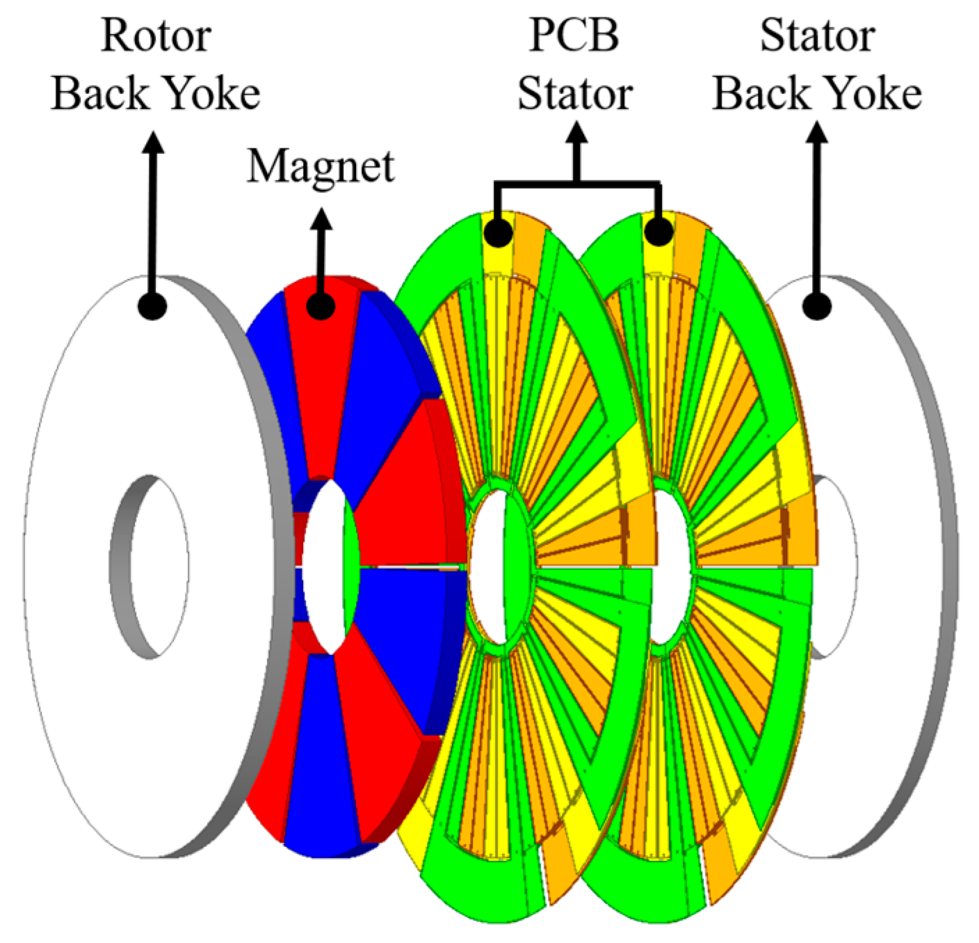
Figure 1. Distributed winding PCB axial flux permanent magnet motor (AFPM).
Actuators 14 00424 g001
Figure 2. (a) Single-phase PCB stator structure. (b) Three-phase PCB stator.
Actuators 14 00424 g002
Figure 3. Cross-sectional view of effective copper traces connected by via holes.
Actuators 14 00424 g003
Figure 4. Cross-sectional structure of the PCB stator.
Actuators 14 00424 g004
Figure 5. Detailed structure of plated via and conductor layers in PCB stator.
Actuators 14 00424 g005
Figure 6. Current flow path through multilayer conductive traces and vias in PCB stator.
Actuators 14 00424 g006
Figure 7. Current density distribution concentrated in the via hole of the conventional model.
Actuators 14 00424 g007
Figure 8. Cross-sectional layout of the via hole, plated barrel.
Actuators 14 00424 g008
Figure 9. Comparison of single-via and multi-via configurations at the inner and outer end-turn regions.
Actuators 14 00424 g009
Figure 10. Inline and grid multi-via placements for PCB stators. Top row: inline configuration (a) inner end turn with sequential vias; (b) outer end turn with sequential vias. Bottom row: grid configuration (c) inner end turn with distributed parallel vias; (d) outer end turn with distributed parallel vias.
Actuators 14 00424 g010
Figure 11. Representative mesh plots for FEM simulations: (a) mesh of PCB stator and via regions used in eddy current analysis for resistance and current density evaluation, (b) mesh discretization of the multilayer PCB circuit for transient electromagnetic simulations, and (c) refined airgap and surrounding airband mesh for transient analysis.
Actuators 14 00424 g011
Figure 12. Phase resistance and peak current density vs. uniform inner/outer via diameter (single-via structure).
Actuators 14 00424 g012
Figure 13. Effect of inner inline multi-via diameter combinations on phase resistance and peak current density.
Actuators 14 00424 g013
Figure 14. Effect of Inner Grid Multi-Via Diameter Combinations on Phase Resistance and Peak Current Density.
Actuators 14 00424 g014
Figure 15. Effect of outer inline multi-via diameter combinations on phase resistance and peak current density.
Actuators 14 00424 g015
Figure 16. Effect of outer grid multi-via diameter combinations on phase resistance and peak current density.
Actuators 14 00424 g016
Figure 17. FEM-based performance maps of the improved grid multi-via PCB stator over the torque–speed operating range.
Actuators 14 00424 g017
Table 1. Design parameters of the PCB AFPM motor model.
ParameterUnitValue
Magnet-N45UH
Rotor-S45C
Stator-35PN230
Number of phases-3
Magnet thicknessmm2.7
Rotor backyoke thicknessmm2.7
Stator backyoke thicknessmm2
Outer diametermm65.4
Inner diametermm20.6
Axial lengthmm10.1
Table 2. 3D Finite element analysis (3D FEA) data.
ParameterUnitConventional Model
Back EMFVrms3.23
Rated SpeedRpm3650
Load TorqueNm0.3
CurrentArms12.37
Current densityA/mm229.46
Copper LossW48.52
AC LossW5.2
Output PowerW114.67
Efficiency%68.10
Table 3. Comparison of 3D finite-element analysis (FEA) results between the conventional and improvement through FEM approach model.
ParameterUnitConventional ModelImprovement Through FEM Approach ModelChange
Back EMFVrms3.23.23-
Load TorqueNm0.30.3-
CurrentArms12.5712.57-
Current densityA/mm242.1933.4520.7%
Phase ResistanceOhm0.1060.08321.7%
Copper LossW50.0839.7020.7%
AC LossW7.117.11-
Output PowerW114.67114.67-
Efficiency%66.7271.016.4%
Disclaimer/Publisher’s Note: The statements, opinions and data contained in all publications are solely those of the individual author(s) and contributor(s) and not of MDPI and/or the editor(s). MDPI and/or the editor(s) disclaim responsibility for any injury to people or property resulting from any ideas, methods, instructions or products referred to in the content.