Article

Optimized Voltage-Induced Control of Magnetic Domain-Wall Propagation in Hybrid Piezoelectric/Magnetostrictive Devices

by
Giancarlo Consolo
1,*,† and
Giovanna Valenti
2,†
1
Department of Mathematics, Computer, Physical and Earth Sciences, University of Messina, 98166 Messina, Italy
2
Department of Engineering, University of Messina, 98166 Messina, Italy
*
Author to whom correspondence should be addressed.
These authors contributed equally to this work.
Actuators 2021, 10(6), 134; https://doi.org/10.3390/act10060134
Submission received: 13 May 2021 / Revised: 14 June 2021 / Accepted: 15 June 2021 / Published: 17 June 2021
(This article belongs to the Special Issue New Design and Applications for Magnetoelastic Actuators)

Abstract

:
A theory of voltage-induced control of magnetic domain walls propagating along the major axis of a magnetostrictive nanostrip, tightly coupled with a ceramic piezoelectric, is developed in the framework of the Landau–Lifshitz–Gilbert equation. It is assumed that the strains undergone by the piezoelectric actuator, subject to an electric field generated by a dc bias voltage applied through a couple of lateral electrodes, are fully transferred to the magnetostrictive layer. Taking into account these piezo-induced strains and considering a magnetostrictive linear elastic material belonging to the cubic crystal class, the magnetoelastic field is analytically determined. Therefore, by using the classical traveling-wave formalism, the explicit expressions of the most important features characterizing the two dynamical regimes of domain-wall propagation have been deduced, and their dependence on the electric field strength has been highlighted. Moreover, some strategies to optimize such a voltage-induced control, based on the choice of the ceramic piezoelectric material and the orientation of dielectric poling and electric field with respect to the reference axes, have been proposed.

1. Introduction

Domain walls (DWs) in ferromagnetic nanostripes have been receiving great attention by researchers both from the theoretical viewpoint [1,2,3] and for their potential applications in DW-based devices, such as memories, logic gates and sensors [4,5,6,7,8]. In these contexts, achieving an effective control of the DW features by means of several external sources, such as magnetic fields, spin-polarized currents and/or electrically-induced mechanical strains, thus becomes fundamental. A great contribution in these research areas has been provided by the employment of magnetostrictive (MS) materials, thanks to their capability of transforming magnetic energy into mechanical energy and vice versa. Further improvements have been obtained by combining piezoelectric (PZ) and magnetoelastic (ME) effects, that have been exploited to build efficient multiferroic heterostructures [9,10,11,12,13,14,15].
In this paper, we aim at accounting for all the above findings to theoretically describe and optimize the control of DWs that move along the major axis of a thin and elongated MS nanostrip placed in tight contact with a thick PZ actuator. Thanks to ME effects, a dc bias voltage applied to the PZ layer generates an electric field that induces deformations of the material that are, in turn, transferred to the adjacent MS layer. Therefore, a hybrid PZ/MS bilayer is a device where an electric field may induce changes of the ME field. Such variations may then be used to tune the key dynamical features associated to DW propagation [12,13,14,15].
In our previous works [16,17,18], in particular, we carried out the mathematical modeling of the above-mentioned magnetization dynamics with particular emphasis on the characterization of the ME field felt by the MS layer as a function of the crystal symmetry (isotropic, cubic or hexagonal). The expressions of the physical quantities there provided were given in terms of the strains generated by the PZ layer, but such strains were left unidentified. Indeed, we only estimated numerically their order of magnitude, but we did not provide their functional dependence on the electric voltage applied across the actuator. However, the analytical predictions carried out in Ref. [16] were compared with experimental results reported in Ref. [13] obtaining a qualitative satisfying agreement, so proving the validity and consistency of our approach.
Starting from such an agreement, here we extend those results with a twofold goal. The first goal consists of establishing an explicit functional dependence of the physical quantities involved in steady and precessional regimes on the electric field generated into the PZ layer via a dc bias voltage. We aim at filling this gap by considering constitutive equations for the piezoelectric layer and solving analytically suitable boundary conditions at the interface between PZ and MS layers. The second goal consists of optimizing the control of DW dynamics as a function of two features: the choice of the ceramic PZ material and the orientation of dielectric poling and electric field.
The manuscript is organized as follows. In Section 2, we present the theoretical framework used to study the propagation of magnetic DWs along the major axis of a MS nanostrip subject to the simultaneous effects arising from dipolar, exchange, anisotropy, Zeeman and ME fields. In particular, the ME field describes the response of a linear elastic cubic MS material and also accounts for the piezo-induced strains. Then, through the classical traveling wave ansatz, the explicit expressions of the key physical quantities characterizing the steady and the precessional regime of DW propagation are deduced and their dependence on the electrical field strength generated is emphasized. In Section 3, we carry out some numerical investigations to quantify the effects of the electric field strength on the physical quantities discussed in the previous section. In particular, some strategies to optimize such a voltage-induced are proposed and discussed. Concluding remarks are given in Section 4.

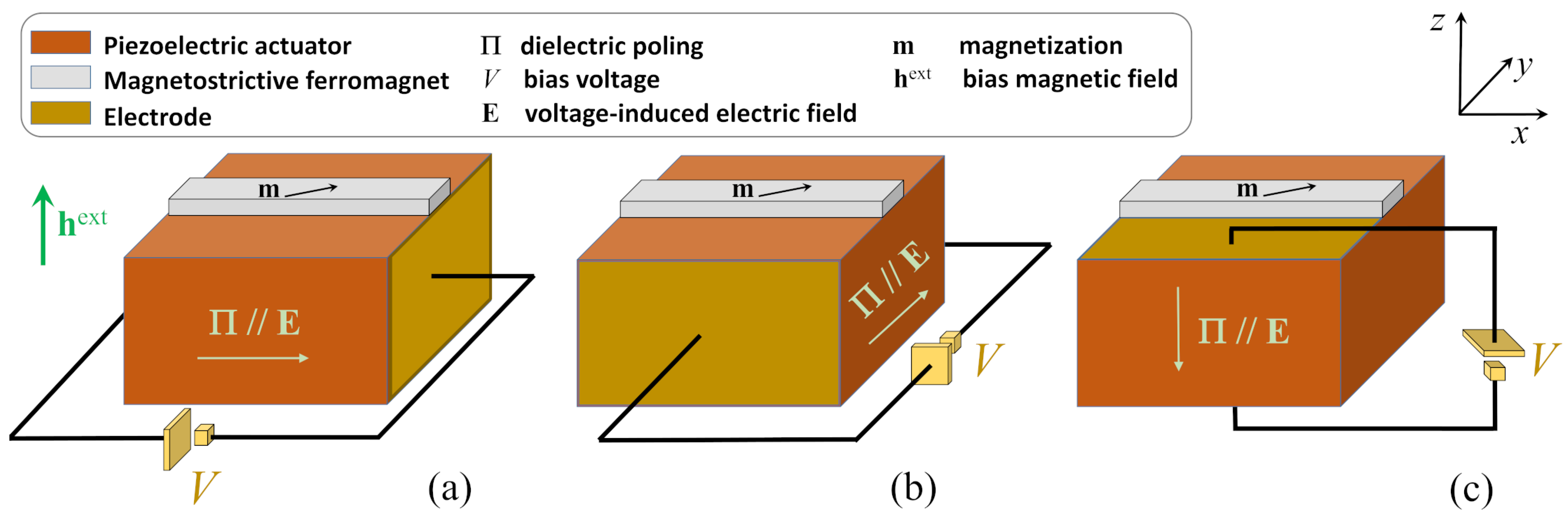
2. Materials and Methods

In this section, we develop the theoretical framework used to describe the propagation of magnetic DWs along the major axis of a thin MS nanostrip placed in tight contact with a PZ actuator. The framework is developed at mesoscopic scale, i.e., the length scale (from a few to ten nanometers) at which one can reasonably discuss magnetization dynamics by averaging the behavior of a few thousands of atoms.
As mentioned in the Introduction, the application of a dc bias voltage via a couple of lateral electrodes generates an electric field into the PZ that is transformed into strains. We assume that these lateral electrodes are placed in such a way that the voltage-induced electric field is always parallel to the dielectric poling field which, in turn, points along one of the reference axes. These assumptions give rise to three different configurations, as schematically depicted in Figure 1.
Let us discuss in more detail the working principle of the hybrid PZ/MS device [12,13,14]. Magnetization dynamics take place in a thin parallelepiped-shape MS nanostrip having the major axis placed along e x axis, width along e y and thickness along e z . It is assumed that a DW, i.e., an intermediate region separating adjacent magnetic domains with different orientations, is nucleated at the center of the nanostrip. The MS layer is surrounded by a constant-in-time and uniform-in-space external bias magnetic field h ext , directed along the e z axis, that drives a 1D motion of the magnetic DW along e x axis, i.e., the major axis of the nanostrip. Owing to the thin and elongated geometry, variations of the physical quantities associated to DW propagation along e y and e z axes can be safely disregarded [16,17,19,20,21,22]. Apart from the external field, DWs are subject to further magnetic fields arising from (short-range) exchange and (long-range) dipolar interactions, magnetocrystalline anisotropy, stress-free magnetostriction and ME effects due to the coupling with the adjacent PZ actuator.
Let us focus on this latter contribution and discuss, in detail, how the application of a dc electric voltage V between two lateral electrodes of a PZ layer may lead to changes of ME field. By applying an electric voltage of a given polarity between two opposite faces of the PZ actuator, the resulting electric field E may induce an elongation or a contraction of the width of the material along the same axis and, in turn, it may lead to a contraction or an elongation in the two orthogonal directions, respectively. By exploiting the thinness of the MS layer and the perfect acoustic contact realized with the adjacent, much thicker, PZ layer, the piezo-induced strains generated at the common interface are transferred from the PZ to the MS. This latter assumption appears to be more than reasonable from the mechanical point of view, considering the negligible thickness of the MS layer in comparison with that of the PZ actuator [12,13,14].
In the 1D approximation, the above field-driven DW dynamics occurring in the MS layer are generally described by means of Landau–Lifshitz–Gilbert (LLG) equation [20,23,24,25,26,27,28] as:
m . = γ h eff m + t d .
In (1), m ( x , t ) stands for the unit magnetization vector characterizing the local spatio-temporal evolution of the state of the MS material, the superposed dot denotes partial time derivative, the coefficient γ = M S μ 0 γ e is expressed in terms of the the saturation magnetization M S , the magnetic permeability of the vacuum μ 0 and of the gyromagnetic ratio γ e = g e / m e (being g the Landè factor, e the electron charge and m e the electron mass), h eff represents the effective magnetic field, whereas t d accounts for all the intrinsic dissipative phenomena.
In detail, the effective field h eff encloses the abovementioned contributions arising from external, exchange, demagnetizing, magnetocrystalline anisotropy and magnetoelastic fields:
h eff = h ext e z + l e x c 2 2 m x 2 N x m x e x + N y m y e y + N z m z e z + h ani + h me ,
In (2), l e x c is the so-called exchange length of the magnetic material, which is related to the exchange constant A exc through l e x c 2 = 2 A exc μ 0 M S 2 . The demagnetizing field is approximated through the demagnetizing factors N x , N y and N z , that fulfill the usual normalization condition N x + N y + N z = 1 . This approximation, usually adopted in the literature to get a rough estimation of the demagnetizing field [29], holds sufficiently well in the middle of the magnetic nanostrip, sufficiently far from the edges, where the field inhomogeneity becomes more relevant. Its use does not hinder our main goal of extracting the dependence of the ME field on the voltage-induced strains.
The magnetocrystalline anisotropy field h ani and magnetoelastic field h me depend on the crystal symmetry of the MS layer, which is here assumed to be cubic and belonging to the crystal classes 4 _ 3m, 432 and m 3 _ m [17,18,30]. For these crystals, the magnetocrystalline anisotropy field can be expressed as:
h ani = 2 K 1 μ 0 M S 2 m x 1 m x 2 e x + m y 1 m y 2 e y + m z 1 m z 2 e z
where K 1 denotes the cubic anisotropy coefficient. By also assuming to deal with a linear elastic material, the magnetoelastic field reads [16,17,18,26,27,28,31,32]:
h me = 1 μ 0 M S 2 ( ϵ ˜ ϵ ˜ m ) : C ˜ : ϵ ˜ m m ,
being ϵ ˜ m the MS strain tensor, ϵ ˜ the total (elastic+magnetostrictive) strain tensor, “:” the double contraction and C ˜ the fourth-order elasticity (or stiffness) tensor. For cubic crystals, the magnetostriction strain tensor ϵ ˜ m is expressed in terms of two MS coefficients, λ 100 and λ 111 , as follows:
ϵ ˜ m = 3 2 λ 100 m x 2 1 3 λ 111 m x m y λ 111 m x m z λ 111 m x m y λ 100 m y 2 1 3 λ 111 m y m z λ 111 m x m z λ 111 m y m z λ 100 m z 2 1 3
whereas the elasticity tensor is expressed in terms of three independent elastic constants c 11 , c 12 and c 44 and, in Voigt notation, takes the form:
C ˜ = c 11 c 12 c 12 c 12 c 11 c 12 [ 0 ] c 12 c 12 c 11 c 44 0 0 [ 0 ] 0 c 44 0 0 0 c 44 .
Then, to identify the six independent components of the total strain tensor ϵ ˜ , we neglect strain variations along the z axis (owing to the small thickness of the MS layer) and apply mechanical boundary conditions at the top and the bottom x y surfaces of the MS layer.
In detail, since the top x y surface is free, the normal components of the Cauchy stress tensor σ ˜ = C ˜ : ( ϵ ˜ ϵ ˜ m ) vanish. Therefore, the boundary condition σ ˜ n = 0 , with n e z the normal to the top surface, leads to:
σ x z = 0 σ y z = 0 σ z z = 0 ϵ x z = 3 2 λ 111 m x m z ϵ y z = 3 2 λ 111 m y m z ϵ z z = c 12 c 11 ϵ x x + ϵ y y + 3 2 λ 100 c 11 c 12 c 11 m z 2 1 3
On the other hand, by assuming an ideal acoustic contact between the PZ and the bottom surface of the MS, the voltage-induced planar strains imposed by the PZ layer are fully transferred to the MS. By introducing the projector on the PZ/MS interface, P i k = I i k n i n k , with I i k the elements of the identity matrix and n i the components of the unit vector orthogonal to the PZ/MS interface, the acoustic contact can be described as:
P i k ϵ k l P Z P l j = P i k ϵ k l P l j = ϵ i j I F ϵ x x P Z = ϵ x x = ϵ x x I F ϵ x y P Z = ϵ x y = ϵ x y I F ϵ y y P Z = ϵ y y = ϵ y y I F
The strains ϵ ˜ P Z generated into the PZ may be correlated to the components of the voltage-induced electric field, E = E x , E y , E z , through the third-order strain-piezoelectric tensor d ˜ as:
ϵ k l P Z = d i j k E k
where the tensor d ˜ depends on the direction of the dielectric polarization Π as well as on the crystal symmetry of the PZ material [33]. We consider a PZ actuator made by a polarized ceramic that, being a transversely isotropic material, allows to define d ˜ in terms of three independent coefficients ( d 1 , d 2 , d 4 ). We also assume that the ceramic PZ layer is polarized along a reference axis ( e x , e y , e z ) and that the electric field E is parallel to Π (see Figure 1). In these three different configurations, the PZ strain tensor reads:
f o r E / / Π / / e x : ϵ ˜ P Z = d 1 0 0 0 d 2 0 0 0 d 2 E x f o r E / / Π / / e y : ϵ ˜ P Z = d 2 0 0 0 d 1 0 0 0 d 2 E y f o r E / / Π / / e z : ϵ ˜ P Z = d 2 0 0 0 d 2 0 0 0 d 1 E z
In (10), we are assuming that the electric field is homogeneously distributed through the PZ layer. However, the exact computation of non-homogeneous depolarizing field that would provide the actual value of the electric field at the PZ/MS interface is beyond the scope of the present paper, as we are only interested in highlighting the functional dependence between mechanical strains and the electric field value at such an interface.
From (10), we deduce that the shear strains acting on the PZ actuator vanish in all the above configurations (and, indeed, the coefficient d 4 never appears in our calculations) so that, also taking into account (7) and (8), the total strain tensor can be expressed as:
ϵ ˜ = ϵ x x P Z 0 3 2 λ 111 m x m z 0 ϵ y y P Z 3 2 λ 111 m y m z 3 2 λ 111 m x m z 3 2 λ 111 m y m z c 12 c 11 ϵ x x P Z + ϵ y y P Z + 3 2 c 11 c 12 c 11 λ 100 m z 2 1 3
where the dependence of the strain components ϵ x x P Z and ϵ y y P Z on the electric field is explicitly given in (10).
Consequently, inserting (5), (6) and (11) into (4), the components of the ME field h me take the form:
h x me = 3 m x μ 0 M S 2 λ 100 c 11 c 12 c 11 β 1 ( E ) 3 c 44 λ 111 2 m y 2 +
+ 3 2 λ 100 2 c 12 c 11 c 11 ( c 11 + c 12 ) ( m x 2 1 3 ) + c 12 ( m y 2 1 3 ) , h y me = 3 m y μ 0 M S 2 λ 100 c 11 c 12 c 11 β 2 ( E ) 3 c 44 λ 111 2 m x 2 +
+ 3 2 λ 100 2 c 12 c 11 c 11 c 12 ( m x 2 1 3 ) + ( c 11 + c 12 ) ( m y 2 1 3 ) ,
h z me = 0
where:
β 1 ( E ) = ( c 11 + c 12 ) d 1 + c 12 d 2 E x for E / / Π / / e x ( c 11 + c 12 ) d 2 + c 12 d 1 E y for E / / Π / / e y ( c 11 + 2 c 12 ) d 2 E z for E / / Π / / e z
β 2 ( E ) = ( c 11 + c 12 ) d 2 + c 12 d 1 E x for E / / Π / / e x ( c 11 + c 12 ) d 1 + c 12 d 2 E y for E / / Π / / e y ( c 11 + 2 c 12 ) d 2 E z for E / / Π / / e z
Finally, the dissipative torque term t d in Equation (1) includes the classical Gilbert damping torque [24,25] as well as the non-linear rate-independent dry friction [16,21,22,34,35], namely:
t d = α G + γ α D m . 1 m m . ,
where the strength of linear and nonlinear dissipation is measured by the phenomenological dimensionless coefficients α G and α D , respectively.
By expressing the unit magnetization vector in polar coordinates θ , φ , inserting (2), (3), (12) and (15) into the LLG Equation (1), we get:
sin θ φ . α G + γ α D θ . 2 + sin 2 θ φ . 2 1 / 2 θ . = γ { l e x c 2 2 θ x 2 + l e x c 2 sin θ cos θ φ x 2 + cos θ cos φ h x me + h x ani cos θ sin φ h y me + h y ani + sin θ h ext + h z ani + + sin θ cos θ N x cos 2 φ + N y sin 2 φ N z } ,
α G + γ α D θ . 2 + sin 2 θ φ . 2 1 / 2 sin θ φ . + θ . = γ { l e x c 2 sin θ 2 φ x 2 + 2 l e x c 2 cos θ θ x φ x + + N x N y sin θ cos φ sin φ + h y me + h y ani cos φ h x me + h x ani sin φ } .
Let us now investigate the above system of governing equations in the two characteristic dynamical regimes: steady and precessional [36]. Let us first consider the steady regime that takes place if the strength of the external sources is below a critical value, usually referred to as Walker breakdown (WB) [20]. Here, DWs undergo a rigid motion along the nanostrip axis e x with constant velocity v, fixed azimuthal angle φ 0 and the polar angle satisfies the classical traveling wave ansatz θ = θ ξ , being ξ = x v t , so that system (16) becomes:
α G v θ + α D ^ = γ { l e x c 2 θ + N x cos 2 φ 0 + N y sin 2 φ 0 N z sin θ cos θ +
+ h ext + h z ani sin θ h x me + h x ani cos φ 0 + h y me + h y ani sin φ 0 cos θ } ,
v θ = γ N x N y sin φ 0 cos φ 0 sin θ + h y me + h y ani cos φ 0 h x me + h x ani sin φ 0 ,
where the prime stands for the derivative with respect to the traveling wave variable ξ and α D ^ = γ α D sign v θ .
Taking into account (3) and (12), Equation (17b) can be recast as:
θ = Γ 1 + k sin 2 θ sin θ ,
where the parameters Γ and k depend on the electric field as follows:
Γ ( E ) = γ 2 v N y N x + 3 λ 100 μ 0 M S 2 c 12 c 11 β 3 ( E ) sin 2 φ 0 ,
k ( E ) = 9 λ 100 2 c 11 c 12 18 λ 111 2 c 44 4 K 1 cos 2 φ 0 sin 2 φ 0 2 μ 0 M S 2 N x N y + 6 λ 100 c 11 c 12 β 3 ( E ) ,
with:
β 3 ( E ) = d 2 d 1 E x for E / / Π / / e x d 1 d 2 E y for E / / Π / / e y 0 for E / / Π / / e z
As it is easy to ascertain, Equation (18) admits two kinds of steady-state solutions corresponding to sin θ = 0 and sin 2 θ = 1 / k (existing for k < 0 only), respectively. The former represents the classical Walker profile of a Bloch DW with θ varying between 0 and 180 [20]; the latter describes the 71 and 109 DW configurations observed in materials with cubic symmetry [1,17]. It should be kept in mind that, according to our previous assumptions, the profile given in (18) strictly holds in the proximity of the DW region, namely close to the interface separating two different domains.
Then, by inserting (18) into (17a), we obtain:
P sin θ + R sin θ cos θ + S sin 3 θ cos θ + Γ k α G v sin 3 θ + 3 γ l e x c 2 k 2 Γ 2 sin 5 θ cos θ + α D ^ = 0 ,
where:
P = Γ α G v γ h ext ,
R = γ { l e x c 2 Γ 2 + N z N y sin 2 φ 0 N x cos 2 φ 0 2 K 1 μ 0 M S 2 + + 3 λ 100 μ 0 M S 2 c 11 c 12 c 11 ϵ x x P Z c 11 cos 2 φ 0 + c 12 + ϵ y y P Z c 11 sin 2 φ 0 + c 12 + λ 100 ( c 11 + 2 c 12 ) 2 } ,
S = γ { 4 k l e x c 2 Γ 2 + 4 K 1 1 cos 2 φ 0 sin 2 φ 0 μ 0 M S 2 18 μ 0 M S 2 c 44 λ 111 2 cos 2 φ 0 sin 2 φ 0 + 9 2 μ 0 M S 2 λ 100 2 c 11 c 12 c 11 c 12 + c 11 1 2 cos 2 φ 0 sin 2 φ 0 } .
Furthermore, by setting R = 0 , we retrieve the expression of the DW width δ = 1 / Γ in terms of magnetostriction, voltage-induced strains and magnetocrystalline anisotropy, as follows:
δ ( E ) = A exc K 1 ψ + μ 0 M S 2 2 N x cos 2 φ 0 + N y sin 2 φ 0 N z ,
where ψ depends on the electric field through the strains ϵ x x P Z and ϵ y y P Z as follows:
ψ = 3 2 λ 100 c 11 c 12 c 11 ϵ x x P Z c 11 cos 2 φ 0 + c 12 + ϵ y y P Z c 11 sin 2 φ 0 + c 12 + λ 100 ( c 11 + 2 c 12 ) 2
Now, in order to deduce the explicit expression of the DW velocity in this regime, under the assumption of a classical Walker profile with 0 θ 180 , it suffices to perform the average of Equation (21) over the DW width:
v ( E ) = 3 α G δ ( E ) 3 + 2 k ( E ) γ h ext π 2 α D ^ ,
which points out the possibility to achieve an electric-field control of the steady DW velocity through the quantities k = k ( E ) and δ = δ ( E ) . To characterize DW dynamics in more detail, let us discuss the functional dependence of three characteristic parameters associated with the steady regime of propagation: DW mobility, propagation threshold and WB field. The former quantity is defined as the sensitivity of the velocity with respect to the strength of the forcing term, i.e., v / h ext which, from (25), is strictly related to the ratio δ ( E ) / 3 + 2 k ( E ) . To compute the propagation threshold, i.e., the minimum value of the external field that allows us to drive the DW motion, we impose in Equation (25) that the DW velocity must be non-negative, so we obtain:
h TH ext = π 2 γ α D ^ .
Equation (26) clearly denotes that the nonlinear dry dissipation is the only mechanism responsible for the threshold, hence the electric field does not play any role in this context. The WB condition constitutes another restriction on the DW velocity that arises from (19a) and takes the form:
v γ δ 2 N x N y + 3 λ 100 c 11 c 12 β 3 ( E ) μ 0 M S 2 .
Combining (25) with (27), it is possible to set the upper boundary of the range in which the external field triggers steady DW dynamics, namely:
h WB ext = π 2 γ α D ^ + α G 3 + 2 k 6 N x N y + 3 λ 100 c 11 c 12 β 3 ( E ) μ 0 M S 2
which turns out to be affected by the electric field through the functions k ( E ) and β 3 ( E ) .
To summarize the results obtained in the steady regime, taking into account all the above functional dependencies (19b), (20), (23), (24), (25), (26) and (28), we can thus conclude that, if dielectric poling Π and electric field E point along e x or e y , then the strength of the electric field generated into the PZ actuator may be used to vary and control the DW width δ , the DW velocity v, the DW mobility ν and the WB field h WB ext . On the other hand, if Π and E are aligned to the e z axis, the electric field affects the DW velocity v only, through variations induced in the DW width δ .
When the external field strength is much larger than WB value, i.e., condition (27) is violated, DW dynamics takes place into the so-called precessional regime. In this case, the DW velocity is not constant anymore and the magnetization vector exhibits periodic in time oscillations at microwave frequency with constant angular speed φ . = ω 0 . Under the above hypotheses, the governing system (16) reads:
ω 0 sin θ + α G v + γ α D v v 2 θ 2 + ω 0 2 sin 2 θ 1 / 2 θ = = γ { N x cos 2 φ + N y sin 2 φ N z sin θ cos θ l e x c 2 θ +
h x me + h x ani cos φ + h y me + h y ani sin φ cos θ + h ext + h z ani sin θ } , α G + γ α D v 2 θ 2 + sin 2 θ ω 0 2 1 / 2 sin θ ω 0 v θ =
= γ N x N y sin θ cos φ sin φ + h y me + h y ani cos φ h x me + h x ani sin φ .
To get an explicit expression of the DW velocity, two further assumptions are made: (i) Equation (18) still qualitatively describes the travelling wave profile in the precessional regime, and (ii) the spatio-temporal dependence of the polar coordinate θ ( x , t ) is approximated by its value at the center of the DW ( θ = π 2 ). Equation (29) can be recast accordingly as follows:
ω 0 + Γ 1 + k α G + γ α D v 2 Γ 2 1 + k 2 + ω 0 2 1 / 2 v = γ h ext , α G + γ α D v 2 Γ 2 1 + k 2 + ω 0 2 1 / 2 ω 0 = Γ v 1 + k + + γ sin φ cos φ { N x N y + 3 λ 100 μ 0 M S 2 c 11 c 12 β 3 +
+ cos 2 φ sin 2 φ μ 0 M S 2 9 2 λ 100 2 c 11 c 12 9 c 44 λ 111 2 2 K 1 }
Then, by performing the average of the Equation (30) over a period of precession, and considering a restriction between average velocity and angular speed, that is generally expressed as Γ 1 + k v ¯ ω 0 , we obtain:
ω 0 + α G Γ 1 + k v ¯ = γ h ext ,
α G ω 0 + γ α D = Γ 1 + k v ¯
from which we deduce the expression of the average DW velocity:
v ¯ ( E ) = γ 1 + α G 2 δ ( E ) 1 + k ( E ) α G h ext + α D .
Expression (32) underlines the feasibility of controlling the DW propagation via electric fields, through k = k ( E ) and δ = δ ( E ) , also in the precessional regime. In particular, the voltage-induced ME effects may alter the DW mobility and modulate the upward shift of the average DW velocity through the ratio δ ( E ) / 1 + k ( E ) .

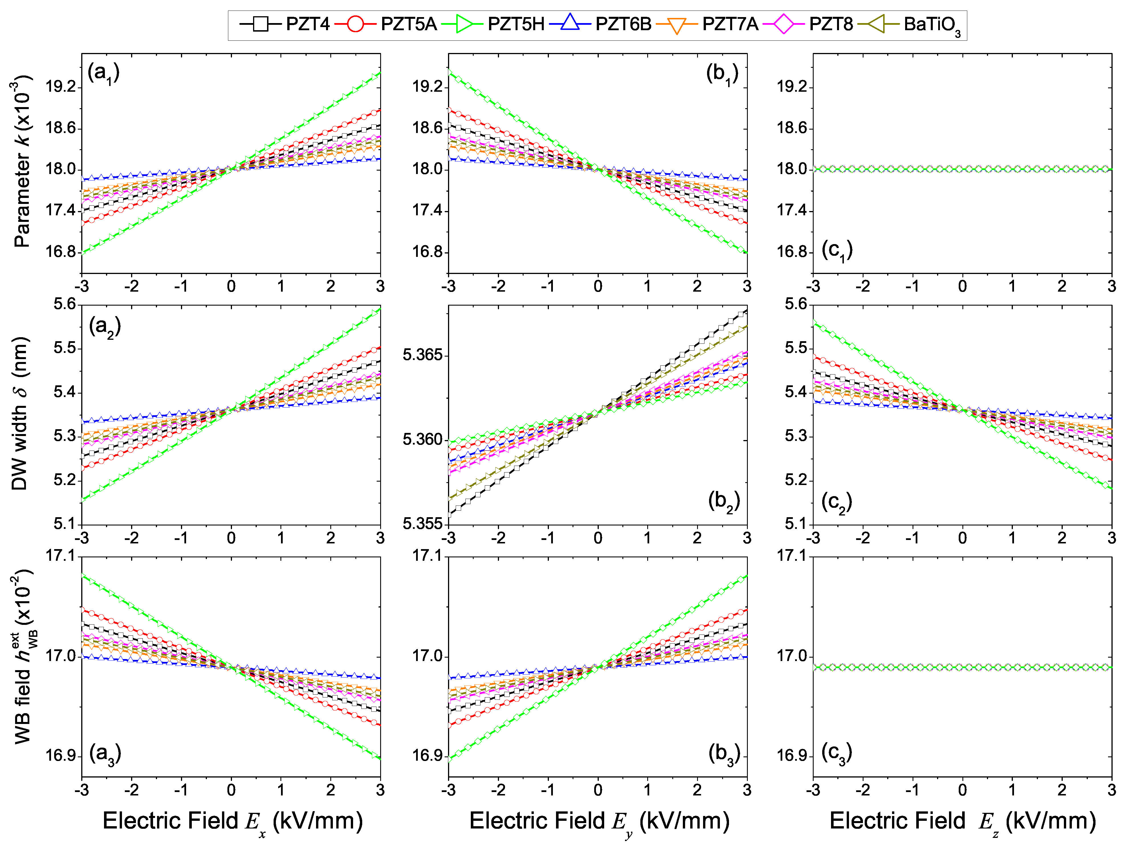
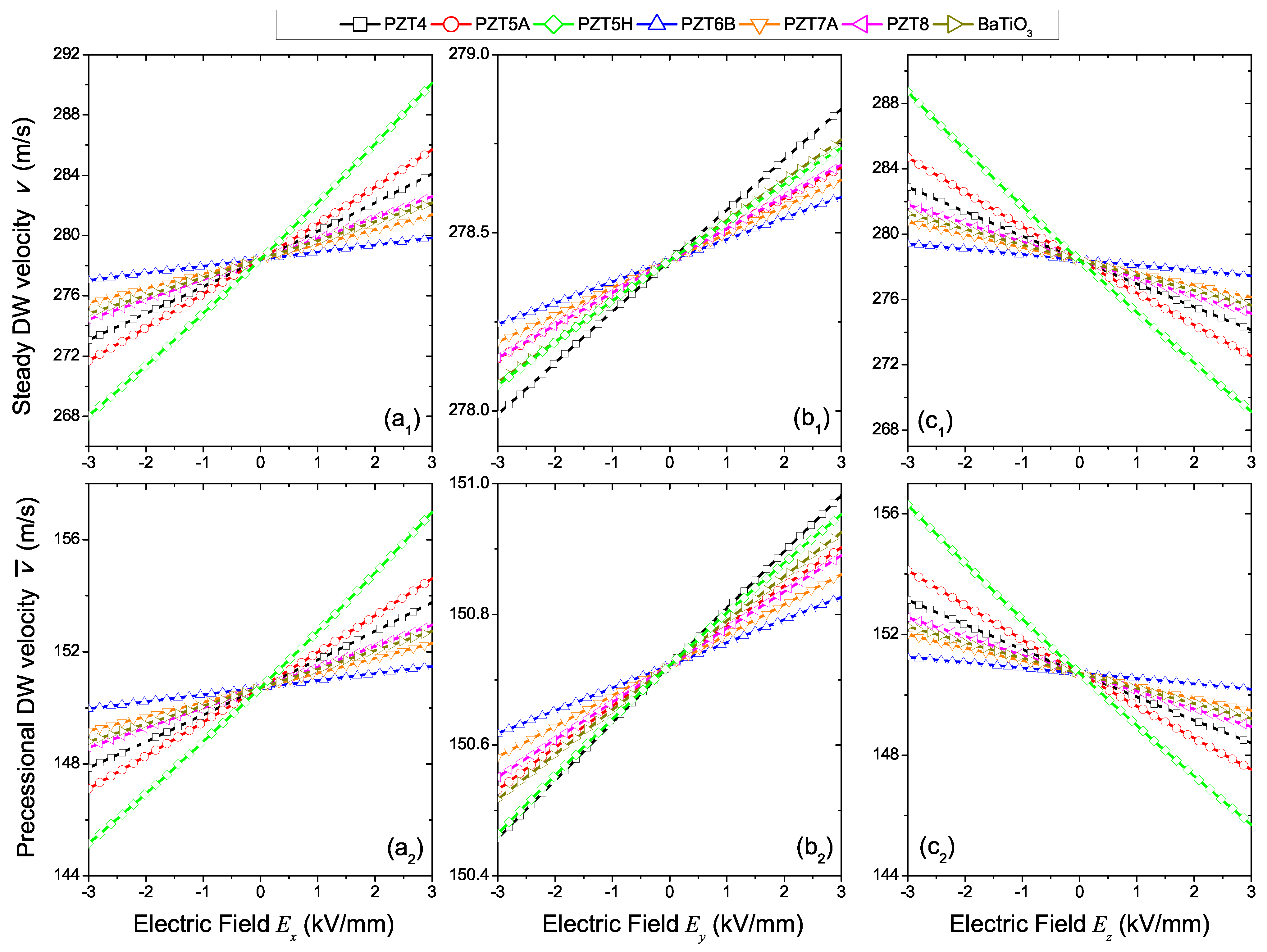
3. Results and Discussion

In the previous section, we computed the key dynamical features associated to steady and precessional dynamical regime and inspected their dependence on the electric field generated into the PZ layer in three different configurations, where the dielectric poling and the electric field are parallel and point along one reference axis. In this section, we evaluate such quantities numerically with the aim of establishing which PZ material, and which common orientation for poling and electric fields, allows us to optimize the voltage response of DWs propagating in a hybrid PZ/MS system.
In our analysis, we consider a Fe 0.8 Ga 0.2 alloy, named Galfenol, as MS ferromagnet exhibiting cubic anisotropy. Moreover, the selection of the most performing PZ actuator is carried out among seven ceramic materials: PZT4, PZT5A, PZT5H, PZT6B, PZT7A, PZT8, and BaTiO3. The values of the corresponding material parameters are summarized in Table 1 and Table 2, respectively.
In Figure 2 and Figure 3, the electric-field dependence of k (19b), δ (23), h WB ext (28), steady (25) and precessional (32) DW velocities is shown for the abovementioned materials and for different orientations of poling and electric fields. In these figures, the strength of the electric field is taken of the same order of magnitude as the one reported in the literature for piezoceramic materials [41,42].
As already seen, the parameter k (top panels of Figure 2) and the WB field h WB ext (bottom panels of Figure 2) do not undergo variations with the electric field, when poling and electric fields point along e z (configuration (c)). On the contrary, if both fields are aligned along e x (configuration (a)) or e y axis (configuration (b)), it is possible to obtain a quasi-linear tuning of the above quantities with a sensitivity that varies according to the choice of the PZ material. Indeed, for the ceramic exhibiting the largest sensitivity, i.e., PZT5H, the parameter k is modulated by about 8 % around the value reported in the absence of any external stimulus ( k ( E = 0 )= 18.0 × 10 3 ), whereas the WB field varies by less than 0.6 % around the value h WB ext ( E = 0 ) = 16.99 × 10 2 . Instead, the material appears to be less sensitive to the electric field is the PZT6B, since the related variations reduce down to less than 1 % for k and to less than 0.06 % for h WB ext . Note, also, that results corresponding to configurations (a) and (b) differ from one another by the slopes of the curves around the values at rest.
A different scenario takes place for the voltage-induced dependence of the DW width δ (middle panels of Figure 2) that is always affected by variations of the electric field, independently of the common orientation of poling and electric fields. However, different sensitivities and slopes are obtained by varying the PZ material and the orientation of the above fields. In detail, starting from the value at rest δ ( E = 0 ) = 5.36 nm, the three proposed configurations allow to get an overall modulation of about 4.5 % in case (a), 0.1 % in case (b) and 4 % in case (c). The above reported best values are provided by PZT5H in configurations (a) and (c), but by PZT4 in setup (b). It should also noticed that, in configuration (b), the PZT5H exhibits the lowest sensitivity to the electric field.
Let us now inspect how the electric-field dependence of the parameters k and δ reflects into the overall DW velocity, in the two investigated dynamical regimes. For simplicity, we fix the external field at a value that falls in the range h TH ext < h ext < h WB ext in the steady regime, whereas it satisfies h ext > h WB ext in the precessional one.
First of all, as one can argue from the comparison of the rows of Figure 3, the electric field response shows no qualitative differences between steady and precessional regime. So, without loss of generality, we shall limit our discussion to the steady regime only. The material that exhibits the largest sensitivity is PZT5H in configurations (a) and (c), but PZT4 in configuration (b). However, the effects arising from sweeping the electric field strength across the PZ layer range over different scales. Indeed, taking into account the reference value v ( E = 0 ) = 278.4 m/s, we get overall variations of about 4 % in case (a), 0.2 % in case (b) and 3.7 % in case (c).
Therefore, if the lateral electrodes need to be placed along the x z axis (configuration (b)), then the ceramic PZ material that provides the better performances is PZT4 whereas, in all other configurations, the material that optimizes the system response is PZT5H. However, it should be remarked that the overall sensitivity of the DW velocity with electric field observed in configuration (b) is about one order of magnitude smaller than those obtained in configurations (a) and (c).
We can thus conclude our theoretical investigations by claiming that, in order to optimize the voltage-control of the DW properties in both dynamical regimes, the optimum setup has to be constituted by a ceramic PZ layer made by PZT5H polarized along the x axis (i.e., along the major axis of the nanostrip) through a couple of lateral electrodes placed on the y z faces.

4. Conclusions

Our theoretical results demonstrated that the propagation of DWs along the major axis of a MS nanostrip, placed on the top of a thick PZ actuator, can be controlled by the electric field generated into the PZ layer via a dc bias voltage. We deduced the explicit expressions of the electric field dependence of the most relevant dynamical features characterizing the steady and the precessional regime of propagation. In particular, we discussed the sensitivity with respect to the electric field of DW width, velocity and mobility, propagation threshold and WB field. Moreover, such functional dependencies were evaluated in three configurations where the dielectric poling and the electric field are collinear and directed along one of the reference axes. Then, we carried out numerical investigations with the main aim of proposing a strategy to optimize the voltage-control of the above described DW propagation. Two key degrees of freedom were considered in such an optimization procedure: the choice of the ceramic PZ material and the common orientation of dielectric polarization and electric field. Our results revealed that the DW velocity exhibits the largest sensitivity on the electric field (modulation up to 4 % ) by using the ceramic PZT5H as PZ actuator, polarizing the dielectric along the x axis and placing the lateral electrodes on the y z faces. When poling and electric fields are aligned to the z axis, a slightly smaller tunability (about 3.7 % ) was achieved by using the same ceramic material. The sensitivity was significantly reduced (by roughly one order of magnitude) when both fields point along the y axis, but in this case the material exhibiting the best performances was the PZT4.
We believe that the proposed theoretical optimization may suggest some useful guidelines for the development of practical tunable sensors based on the propagation of magnetic DWs. Finally, we aim at further extending the framework here discussed in the context of spin-orbitronic technologies, where thin magnetic layers exhibit perpendicular anisotropy and/or Dzyaloshinskii-Moriya interaction, as well as in antiferromagnetically-coupled devices.

Author Contributions

Conceptualization, formal analysis, investigation and validation, G.C. and G.V.; software and visualization, G.C.; writing—original draft preparation, G.C.; writing—review and editing, G.V. All authors have read and agreed to the published version of the manuscript.

Funding

This research was funded by MUR (Italian Ministry of University and Research) through project PRIN2017 no.2017YBKNCE, “Multiscale phenomena in Continuum Mechanics: singular limits, off-equilibrium and transitions” and by INdAM-GNFM.

Institutional Review Board Statement

Not applicable.

Informed Consent Statement

Not applicable.

Conflicts of Interest

The authors declare no conflict of interest.

Abbreviations

The following abbreviations are used in this manuscript:
PZPiezoelectric
MSMagnetostrictive
MEMagnetoelastic
DWDomain-Wall
LLGLandau-Lifshitz-Gilbert equation
WBWalker Breakdown

References

  1. Hubert, A.; Schäfer, R. Magnetic Domains: The Analysis of Magnetic Microstructures; Springer: Berlin/Heidelberg, Germany, 2008. [Google Scholar]
  2. Chikazumi, S.; Graham, C.D. Physics of Ferromagnetism; Oxford University Press: Oxford, UK, 2009. [Google Scholar]
  3. Cullity, B.D.; Graham, C.D. Introduction to Magnetic Materials; Wiley: New York, NY, USA, 2009. [Google Scholar]
  4. Atkinson, D.; Eastwood, D.S.; Bogart, L.K. Controlling domain wall pinning in planar nanowires by selecting domain wall type and its application in a memory concept. Appl. Phys. Lett. 2008, 92, 022510. [Google Scholar] [CrossRef] [Green Version]
  5. Ono, T.; Nakatani, Y. Magnetic domain wall oscillator. Appl. Phys. Exp. 2008, 1, 061301. [Google Scholar] [CrossRef]
  6. Allwood, D.; Xiong, G.; Cooke, M.D.; Faulkner, C.C.; Atkinson, D.; Vernier, N.; Cowburn, R.P. Submicrometer ferromagnetic NOT gate and shift register. Science 2002, 296, 2003–2006. [Google Scholar] [CrossRef] [PubMed]
  7. Allwood, D.A.; Xiong, G.; Faulkner, C.C.; Atkinson, D.; Petit, D.; Cowburn, R.P. Magnetic domain-wall logic. Science 2005, 309, 1688–1692. [Google Scholar] [CrossRef] [PubMed]
  8. Xu, P.; Xia, K.; Gu, C.; Tang, L.; Yang, H.; Li, J. An all-metallic logic gate based on current-driven domain wall motion. Nat. Nanotechnol. 2008, 3, 97–100. [Google Scholar] [CrossRef]
  9. Eerenstein, W.; Mathur, N.D.; Scott, J.F. Multiferroic and magnetoelectric materials. Nature 2006, 442, 759–765. [Google Scholar] [CrossRef]
  10. Vaz, C.A.; Hoffman, J.; Ahn, C.H.; Ramesh, R. Magnetoelectric coupling effects in multiferroic complex oxide. Adv. Mater. 2010, 22, 2900–2918. [Google Scholar] [CrossRef]
  11. Balinskiy, M.; Chavez, A.C.; Barra, A.; Chiang, H.; Carman, G.P.; Khitun, A. Magnetoelectric spin wave modulator based on synthetic multiferroic structure. Sci. Rep. 2018, 8, 10867. [Google Scholar] [CrossRef]
  12. Lei, N.; Devolder, T.; Agnus, G.; Aubert, P.; Daniel, L.; Kim, J.V.; Zhao, W.; Trypiniotis, T.; Cowburn, R.P.; Chappert, C.; et al. Strain-controlled magnetic domain wall propagation in hybrid piezoelectric/ferromagnetic structures. Nat. Commun. 2013, 4, 1378. [Google Scholar] [CrossRef]
  13. De Ranieri, E.; Roy, P.E.; Fang, D.; Vehsthedt, E.K.; Irvine, A.C.; Heiss, D.; Casiraghi, A.; Campion, R.P.; Gallagher, B.L.; Jungwirth, T.; et al. Piezoelectric control of the mobility of a domain wall driven by adiabatic and non-adiabatic torques. Nat. Mater. 2013, 12, 808–814. [Google Scholar] [CrossRef]
  14. Shepley, P.M.; Rushforth, A.W.; Wang, M.; Burnell, G.; Moore, T.A. Modification of perpendicular magnetic anisotropy and domain wall velocity in Pt/Co/Pt by voltage-induced strain. Sci. Rep. 2015, 5, 7921. [Google Scholar] [CrossRef] [Green Version]
  15. Hu, J.M.; Yang, T.; Momeni, K.; Cheng, X.; Chen, L.; Lei, S.; Zhang, S.; Trolier-McKinstry, S.; Gopalan, V.; Carman, G.P.; et al. Fast magnetic domain-wall motion in a ring-shaped nanowire driven by a voltage. Nano Lett. 2016, 16, 2341–2348. [Google Scholar] [CrossRef] [PubMed]
  16. Consolo, G.; Valenti, G. Analytical solution of the strain-controlled magnetic domain wall motion in bilayer piezoelectric/magnetostrictive nanostructures. J. Appl. Phys. 2017, 121, 043903. [Google Scholar] [CrossRef]
  17. Consolo, G.; Valenti, G. Strain-mediated propagation of magnetic domain-walls in cubic magnetostrictive materials. Ric. Matem. 2021, 70, 81–97. [Google Scholar] [CrossRef]
  18. Consolo, G.; Federico, S.; Valenti, G. Magnetostriction in transversely isotropic hexagonal crystals. Phys. Rev. B 2020, 101, 014405. [Google Scholar] [CrossRef]
  19. Zhang, S.; Li, Z. Roles of nonequilibrium conduction electrons on the magnetization dynamics of ferromagnets. Phys. Rev. Lett. 2004, 93, 127204. [Google Scholar] [CrossRef] [Green Version]
  20. Schryer, N.L.; Walker, L.R. The motion of 180deg domain walls in uniform dc magnetic fields. J. Appl. Phys. 1974, 45, 5406–5421. [Google Scholar] [CrossRef]
  21. Consolo, G.; Currò, C.; Martinez, E.; Valenti, G. Mathematical modeling and numerical simulation of domain wall motion in magnetic nanostrips with crystallographic defects. Appl. Mathem. Modell. 2012, 36, 4876–4886. [Google Scholar] [CrossRef]
  22. Consolo, G.; Valenti, G. Traveling wave solutions of the one-dimensional extended Landau-Lifshitz-Gilbert equation with nonlinear dry and viscous dissipations. Acta Appl. Mathem. 2012, 122, 141–152. [Google Scholar] [CrossRef]
  23. Landau, L.D.; Lifshitz, E.M. On the theory of the dispersion of magnetic permeability in ferromagnetic bodies. Phys. Zeits. Sowjetun. 1935, 8, 153–169. [Google Scholar]
  24. Gilbert, T.L. A lagrangian formulation of the gyromagnetic equation of the magnetization field. Phys. Rev. 1955, 100, 1243. [Google Scholar]
  25. Tiberkevich, V.; Slavin, A. Nonlinear phenomenological model of magnetic dissipation for large precession angles: Generalization of the gilbert model. Phys. Rev. B 2007, 75, 014440. [Google Scholar] [CrossRef]
  26. Shu, Y.C.; Lin, M.P.; Wu, K.C. Micromagnetic modeling of magnetostrictive materials under intrinsic stress. Mech. Mater. 2004, 36, 975–997. [Google Scholar] [CrossRef]
  27. Baňas, L. A numerical method for the Landau–Lifshitz equation with magnetostriction. Math. Meth. Appl. Sci. 2005, 28, 1939–1954. [Google Scholar] [CrossRef]
  28. Liang, C.Y.; Keller, S.M.; Sepulveda, A.E.; Bur, A.; Sun, W.Y.; Wetzlar, K.; Carman, G.P. Modeling of magnetoelastic nanostructures with a fully coupled mechanical-micromagnetic model. Nanotechnology 2014, 25, 435701. [Google Scholar] [CrossRef] [Green Version]
  29. Mougin, A.; Cormier, M.; Adam, J.P.; Metaxas, P.J.; Ferre’, J. Domain wall mobility, stability and Walker breakdown in magnetic nanowires. Eur. Phys. Lett. 2007, 78, 57007. [Google Scholar] [CrossRef] [Green Version]
  30. Federico, S.; Consolo, G.; Valenti, G. Tensor representation of magnetostriction for all crystal classes. Math. Mech. Solids 2019, 24, 2814–2843. [Google Scholar] [CrossRef]
  31. Zhang, J.X.; Chen, L.Q. Phase-field microelasticity theory and micromagnetic simulations of domain structures in giant magnetostrictive materials. Acta Mater. 2005, 53, 2845–2855. [Google Scholar] [CrossRef]
  32. Mballa-Mballa, F.S.; Hubert, O.; He, S.; Depeyre, S.; Meilland, P. Micromagnetic modeling of magneto-mechanical behavior. IEEE Trans. Magn. 2014, 50, 1–4. [Google Scholar] [CrossRef] [Green Version]
  33. Yang, J. An Introduction to the Theory of Piezoelectricity; Springer: Boston, MA, USA, 2006. [Google Scholar]
  34. Baltensperger, W.; Helman, J.S. A model that gives rise to effective dry friction in micromagnetics. J. Appl. Phys. 1993, 73, 6516–6518. [Google Scholar] [CrossRef]
  35. Min, H.; McMichael, R.D.; Donahue, M.J.; Miltat, J.; Stiles, M.D. Effects of disorder and internal dynamics on vortex wall propagation. Phys. Rev. Lett. 2010, 104, 217201. [Google Scholar] [CrossRef] [Green Version]
  36. Metaxas, P.J.; Jamet, J.P.; Mougin, A.; Cormier, M.; Ferré, J.; Baltz, V.; Rodmacq, B.; Dieny, B.; Stamps, R.L. Creep and flow regimes of magnetic domain-wall motion in ultrathin Pt/Co/Pt films with perpendicular anisotropy. Phys. Rev. Lett. 2007, 99, 217208. [Google Scholar] [CrossRef] [Green Version]
  37. Gopman, D.B.; Sampath, V.; Ahmad, H.; Bandyopadhyay, S.; Atulasimha, J. Static and dynamic magnetic properties of sputtered Fe-Ga thin films. IEEE Trans. Magn. 2017, 53, 1–4. [Google Scholar] [CrossRef] [Green Version]
  38. Clark, A.E.; Hathaway, K.B.; Wun-Fogle, M.; Restorff, J.B.; Lograsso, T.A.; Keppens, V.M.; Petculescu, G.; Taylor, R.A. Extraordinary magnetoelasticity and lattice softening in bcc fe-ga alloys. J. Appl. Phys. 2003, 93, 8621–8623. [Google Scholar] [CrossRef] [Green Version]
  39. Wuttig, M.; Dai, L.; Cullen, J.R. Elasticity and magnetoelasticity of Fe-Ga solid solutions. Appl. Phys. Lett. 2002, 80, 1135–1137. [Google Scholar] [CrossRef]
  40. Rafique, S.; Cullen, J.R.; Wuttig, M.; Cui, J. Magnetic anisotropy of FeGa alloys. J. Appl. Phys. 2004, 95, 6939–6941. [Google Scholar] [CrossRef]
  41. Esteves, G.; Fanchera, C.M.; Röhrig, S.; Maierc, G.A.; Jones, J.L.; Deluca, M. Electric-field-induced structural changes in multilayer piezoelectric actuators during electrical and mechanical loading. Acta Mater. 2017, 132, 96–105. [Google Scholar] [CrossRef]
  42. Bruno, B.P.; Fahmy, A.R.; Stürmer, M.; Wallrabe, U.; Wapler, M.C. Properties of piezoceramic materials in high electric field actuator applications. Smart Mater. Struct. 2019, 28, 015029. [Google Scholar] [CrossRef]
Figure 1. Layout of the three investigated configurations of the hybrid PZ/MS device where the dielectric poling and the voltage-induced electric field are collinear and aligned to the: (a) e x axis, (b) e y axis or (c) e z axis.
Actuators 10 00134 g001
Figure 2. Electric-field dependence of parameter k (top panels), DW width δ (middle panels) and WB field h WB ext (bottom panels) in the three proposed configurations: (a1a3) E / / Π / / e x , (b1b3) E / / Π / / e y and (c1c3) E / / Π / / e z , for the seven ceramic PZ materials taken into account (depicted in the top legend).
Actuators 10 00134 g002
Figure 3. Electric-field dependence of steady (top panels) and precessional (bottom panels) velocity in the three proposed configurations, (a1,a2) E / / Π / / e x , (b1,b2) E / / Π / / e y and (c1,c2) E / / Π / / e z , for the seven ceramic PZ materials taken into account (depicted in the top legend). Steady and precessional velocities are obtained by fixing the bias magnetic field at h ext = 16 . 5 × 10 2 and h ext = 20 × 10 2 , respectively. These values fulfill the restrictions reported in the main text.
Actuators 10 00134 g003
Table 1. Numerical values of parameters characterizing the Galfenol-based MS layer.
QuantityUnitValueRef.
μ 0 M S T1.5[37]
A exc pJ/m14[37]
α G 0.04[37]
3 2 λ 100 + 400 × 10 6 [38,39]
3 2 λ 111 + 40 × 10 6 [38,39]
c 11 GPa200[38,39]
c 12 GPa160[38,39]
c 44 GPa130[38,39]
K 1 J / m 3 0.5 × 10 4 [40]
N x 0.6424assumed
N y 0.0092assumed
N z 0.3484assumed
φ 0 deg10assumed
α D 0.1assumed
Table 2. Numerical values of the PZ coefficients d 1 and d 2 ( × 10 10 ) associated to different ceramic materials. Values are extracted from Ref. [33].
Materiald1d2
PZT4+2.89−1.23
PZT5A+3.74−1.71
PZT5H+5.92−2.74
PZT6B+0.72−0.27
PZT7A+1.53−0.65
PZT8+2.15−0.93
BaTiO3+1.91−0.79
Publisher’s Note: MDPI stays neutral with regard to jurisdictional claims in published maps and institutional affiliations.

