Article

Comparing In Situ DIC Results from an Etched Surface with a Gold Speckled Surface

by
Christian Oen Paulsen
1,2,*,†,
Egil Fagerholt
2,3,†,
Tore Børvik
2,3,† and
Ida Westermann
1,2,†
1
Department of Materials Science and Engineering, Norwegian University of Science and Technology (NTNU), NO-7491 Trondheim, Norway
2
Centre for Advanced Structural Analysis (CASA), NTNU, NO-7491 Trondheim, Norway
3
Structural Impact Laboratory (SIMLab), Department of Structural Engineering, NTNU, NO-7491 Trondheim, Norway
*
Author to whom correspondence should be addressed.
These authors contributed equally to this work.
Metals 2019, 9(8), 820; https://doi.org/10.3390/met9080820
Submission received: 22 June 2019 / Revised: 16 July 2019 / Accepted: 22 July 2019 / Published: 25 July 2019
(This article belongs to the Special Issue Quasi-Static and Dynamic Testing of Metallic Materials)

Abstract

:
A ferrite-pearlite two-phase steel was investigated using in situ scanning electron microscope (SEM) tensile testing combined with digital image correlation (DIC). Two different speckled patterns were used and compared. The first pattern was achieved by etching a polished surface in order to reveal the microstructural features. Second, a gold speckled pattern was obtained. Here, a continuous layer of gold was applied to a polished surface. This continuous layer was remodeled into gold nanoparticles by keeping the specimen at 180 °C for 96 h with an Ar/Styrene mixture flowing across the specimen surface. The result is randomly distributed gold nanoparticles on the surface. These particles and the etched microstructure were then used by the DIC software to correlate an image series to obtain the local strain field of the material. The differences between the two techniques are numerous. Considering the etched surface, most microstructural features were grain boundaries and pearlite lamellas. As a consequence, large areas within grains did not provide sufficient contrast for DIC, thus restricting maximum resolution. However, the technique is fast and does not expose the material to any elevated temperatures. In contrast, the gold remodeling method provides a finely dispersed gold speckle pattern on the surface, giving excellent contrast across the recorded area. DIC with gold particles achieved a spatial resolution of 0.096 µm, compared to 2.24 µm in the DIC for the etched specimen. As a result, DIC with gold speckles can resolve slip lines. Conversely, DIC with etched microstructure resolves local strains on grain level. However, it is less cumbersome and faster to perform the test on the etched specimen.

1. Introduction

The industry commonly uses steels with a ferritic-pearlitic microstructure. In such steels, the properties of the soft ferrite are combined with the harder pearlite to achieve a good combination of strength and ductility [1]. Knowing the heterogeneous strain field at the grain scale is an important tool in order to understand the relationship between the microstructure and the elastoplastic response. Elastic deformations are reversible, meaning that the material returns to its original shape when the applied loads are released. On the other hand, plastic deformations are permanent, introducing non-reversible changes and damage to the material. During plastic deformation, typically micro-void formation or micro-cracking is the dominating damaging mechanism leading to fracture [2]. Thus, a thorough understanding of these processes is important in the design of steel structures.
Some studies have looked into the deformation process of pearlite. For instance, an early work using the in situ scanning electron microscope (SEM) technique was performed by Porter et al. [3]. They were able to study the effect of coarse versus fine pearlite and show how the deformation process of the two phases differed. Building on their work, Sidhom et al. [4] combined in situ SEM with electron backscatter diffraction (EBSD) to correlate the observations with the different orientations of the grains. The conclusion from this investigation was that coarse pearlite has a more brittle behavior than fine pearlite during tensile deformation. As a result, the damage caused by the plastic deformation was found to be somewhat delayed by incorporating a fine pearlitic structure.
Peters and Ranson [5] published one of the earliest papers on the use of digital image correlation (DIC) in mechanical testing and later others further developed the technique [6,7,8,9,10,11,12,13]. Recently, the DIC technique has caught interest for images acquired with an SEM [14,15,16]. All that is required for DIC is an image series of the desired region containing a speckled pattern with sufficient contrast and the pixel-to-mm ratio. Using an SEM, it is possible to record high-resolution images with high magnification. These images can be correlated using DIC to get strain fields which can resolve the slip bands within grains (see, e.g., [16,17,18,19,20]). A challenge is to have a speckled pattern suitable for DIC analysis. Several different approaches are taken, depending on the desired resolution. Allais et al. [21] developed a technique using a micro-grid to measure the local strains in a dual phase (DP) steel. This micro-grid consisted of several hundred gold dots. These were deposited on the surface using a microelectrolithographic technique. The technique is briefly described here and is based on Appendix A in Allais et al. [21]. First, the surface is covered with a thin layer of an electro-sensitive resin. To polymerize the resin, it was cured for 30 min at 140 °C. The desired pattern was drawn using the SEM electron beam. This irradiation lowered the molecular weight of the resin, making it easily soluble. After the dotted pattern was created, the resin inside the dots was dissolved using a solvent, before a gold layer was applied to the specimen surface. Finally, the remaining resin was then dissolved using a different solvent, leaving only the dotted gold micro-grid pattern on the surface. The displacement of the gold dots during an in situ SEM tensile test was used to calculate the strain field in the microstructure. The resulting spatial resolution was 0.5–1 µm. Several other techniques have been utilized over the years to study the local straining of a microstructure, including, but not limited to: etching, surface deposition and creation of micro-grids using electron beam lithography [16,22,23,24,25].
One technique not mentioned above is to use secondary electron images of the microstructure. These images can then be correlated to find local strain values and distributions. The technique relies on using the variation of gray-scale values in the recorded micrographs without any adaptations (such as adding a micro-grid or a speckled pattern). The features in the microstructure (grain boundaries, particles, different phases, etc.) are used as reference points for the subsequent DIC analysis. Using the microstructure of the specimen to correlate images was first shown by Kang et al. [26] and later by others [15,27,28,29,30,31,32]. Ghadbeigi et al. [27] compared results from DIC using the microstructure as a reference to the micro-grid method. The results were quantitatively similar for the two techniques, demonstrating the reliability of using the microstructure directly for the DIC analysis. Banerjee et al. [30] correlated SEM topography images based on micrographs to investigate the local strain variations in a grain of high strength steel. The applied global strain in that study was 8.3%, but locally, inside a grain, strain values as high as 150% were observed. Other grains were found to have a local average strain value of 1.9%. In the study by Kang et al. [26], a micrograph was acquired for every 3–5% of macroscopic strain and then loaded into a DIC software and correlated to obtain the microscopic strain field.
Recent advances in in situ SEM DIC is the ability to get higher spatial resolution. For instance, Orozco-Caballero et al. [18] achieved a spatial resolution of 44 nm in their strain fields. This fine resolution is accomplished by using a refined method developed by Gioacchino and da Fonseca [16]. Orozco-Caballero et al. [18] applied a gold speckled pattern on a magnesium alloy. This pattern provides great contrast between the specimen surface and the gold particles in an SEM BSE image, providing excellent conditions for DIC analysis. The resulting strain field in a magnesium alloy is capable of resolving slip bands within grains, thereby quantifying the strain ratio between these bands, the grain boundaries, and the overall average strain.
The main objective of the current study was to demonstrate the difference between two techniques for in situ SEM tensile testing. In these techniques, two different specimen preparation methods were used, in combination with two different SEM imaging modes. For both methods, the same steel was used, i.e., an NVE36 ferritic-pearlitic rolled plate steel. The first method presented uses an etched specimen surface. Here, the grain boundaries and the lamellar structure of pearlite provides contrast for the DIC using an secondary electron (SE) imaging mode when recording the microstructure. However, inside the ferrite grains, there is little contrast for the DIC. The second method uses a gold speckled pattern applied to correlate the images in the DIC. This method provides excellent contrast for DIC when recording in backscatter electron (BSE) imaging mode. Compared to etching the specimen surface to obtain contrast for SEM imaging, applying a gold speckled pattern takes much longer time and exposes the specimen for an elevated temperature. However, the spatial resolution in the DIC is much higher.

2. Material

The specimens used in this study were taken from a commercial ferritic-pearlitic rolled steel plate, named NVE36, with chemical composition as listed in Table 1. This steel contains 75% ferrite and 25% pearlite, with an average grain diameter of 15 µm. Figure 1 illustrates the microstructure of the material, where the darker grains are ferrite, and the lighter grains are pearlite. Micro-hardness measurements of the ferrite and pearlite gave average hardness values of 204 HV and 283 HV, respectively. The hardness measurements were performed with 10 g of force and a holding time of 15 s. The combination of the two phases gives an alloy with superior strength and ductility compared to having a pure ferritic or pearlitic microstructure. To make sure that the observed area is in the necked region and close to the fracture initiation point, a notched specimen geometry was chosen. All specimens used in this work were taken parallel to the rolling direction of the larger plate, with a thickness of 10 mm, illustrated in Figure 2a. Then, the specimens were spark eroded to a 2 mm thickness to the dimensions shown in Figure 2b. To reveal the microstructure in SE imaging mode, the specimens were prepared by mechanical grinding and polishing to 1 µm, followed by etching for 10 s in 2% Nital. In addition, the specimens were prepared for EBSD analysis and subsequent application of a gold speckled pattern (see Section 4.3). These specimens were also prepared by mechanical grinding and polishing to 1 µm, before vibration polishing using a VibroMet2 from Buehler (Lake Bluff, IL, USA) for 16 h. In the vibration polisher, there is a suspension with pH 8 containing SiO2 particles with the size 0.02 µm. Finally, all specimens were rinsed in an ultrasonic bath with acetone for 5 min to obtain a clean surface finish.

3. Digital Image Correlation

Digital Image Correlation (DIC) has become a well-established tool for full-field displacement and strain measurements during mechanical testing. Various formulations of DIC exist in the literature, where the principle of optical flow forms the basis for the technique. The traditional formulation of DIC (see, e.g., Sutton et al. [6]) is the subset-based formulation, where subsets are optimized individually. In contrast, the finite-element (FE) formulation of DIC proposed by Besnard et al. [10] is a global approach where the parameters describing the displacement field are solved in a single global procedure. FE-DIC uses a mesh of two-dimensional elements to describe the displacement field, and the degrees-of-freedom (DOF) of the elements are optimized for each image in the series. Various types of elements have been investigated in the literature (see, e.g., Réthoré et al. [12]) and the technique is in principle independent of the choice of the element type. However, Q4 elements (elements with four nodes and eight DOFs) are the most used. The reader is referred to Fagerholt [34] for the mathematical details of the FE-DIC approach applied in this study.
From the principle of optical flow, DIC assumes all images in a series to be a transformed version of the reference image, where the displacement field gives the transformation. Thus, effects such as gray-scale pixel noise (or signal-to-noise ratio), light variations, propagating cracks, etc., cause increasing residuals in the DIC optimization process and pose challenges to the algorithm. The pixel noise must be considered in the design and setup of the experiment, in terms of choice of camera, lighting conditions, room temperature, etc. In the analysis stage, it is possible to increase the element size to overcome a high noise level, with the downside of losing resolution in the displacement field measurements. Temporal changes in the ambient lighting conditions during the test may be optimized by a normalization of the pixel gray values. Here, an elementwise normalization based on both mean and variance of the gray-scale values is applied, i.e., using a zero-mean normalized sum of squared differences (ZNSSD) criterion [14]. Updating of reference images in the DIC algorithm acts as a reset of gray-scale value residuals and can be used when the appearance of the specimen surface has deviated significantly from the reference image. Reference updates may be challenging and should, in general, be reduced to a minimum because errors in the displacement field are accumulated, as also discussed by Tang et al. [35].
When studying the etched specimen, reference updates were crucial to be able to analyze the specimen until fracture and to overcome the deviations in specimen surface appearance, as seen in the SE micrographs. Further, a robust DIC algorithm needs functionality to overcome large jumps in displacements between succeeding images in a series. As the series of micrographs recorded in the SEM needed continuous manual re-positioning of the specimen, such jumps were present for all micrographs. To overcome this, a multi-scale coarse-search procedure motivated by Hild et al. [36] was applied. Calibration of the SEM recordings (drift and spatial distortion) [14] were also considered. However, due to the relatively low magnification and short exposure time in these tests, these effects were assumed small. The error caused by spatial distortion was, however, quantified in a simple test with a rigid moving specimen (see the last paragraph in Section 5).
Most strains in this study are referred to as average engineering strains. These strains are calculated using virtual extensometers in the DIC software, defined as a vector between two material points in the DIC mesh. The average engineering strain ( e ¯ D I C ) is then calculated as
e ¯ D I C = i = 1 N e D I C i , e D I C i = Δ L L 0
where L 0 is the initial length of the virtual extensometer (vector), and Δ L is the change in length of the virtual extensometer (vector).
Local strain at the nodes is calculated as principal logarithmic strains at element level (see, e.g., [37]). Here, X = ( X , Y ) refers to the image coordinates in the reference configuration and bold variables denotes vectors. First, the deformation gradient F = F ( X , t ) = 1 + u / X is found from the measured two-dimensional displacement field u = u ( X , t ) for a particular location X and time t. The right Cauchy–Green tensor is then calculated as
C = F T F
The principal stretches μ i , i = 1 , 2 are found by solving the eigenvalue problem for the right Cauchy–Green tensor
( μ i 2 1 - C ) n i = 0
where the vectors n i gives the direction of the principal stretches μ i . The in-plane logarithmic principal strains ε i = ε i ( X , t ) are finally found as
ε i = ln ( μ i ) , i = 1 , 2
The index i is arranged so that ε 1 > ε 2 . In this work, the major logarithmic principal strain ε i was used for visualization of the strain fields as well as to access the local maximum strain within a DIC element (and named ε D I C ). These measured strains were eventually compared to the corresponding maximum principal strains.

4. Experimental

4.1. Tensile Testing Using In Situ SEM Stage

The experimental work was based on in situ tensile testing in SEM. The in situ device used is shown in Figure 3. This is a spindle-driven device, with the outer dimensions 155 mm × 95 mm × 45 mm. The device is placed inside the vacuum chamber, where it is mounted on top of the SEM stage after removal of the rotation unit. It consists of a rigid frame with two gripping cross-heads, where one is movable, and the other one is fixed. An electrical direct current motor drives the movable cross-head. During testing, the displacement and load transducers record the elongation and applied force, respectively. Additional modules for the device can be mounted to provide other deformation modes, such as compression and bending. For further reading and previous use of the in situ SEM device, the reader is referred to [38,39,40]. During an in situ SEM tensile test, a selected area was recorded with a series of images of the microstructure. These images were recorded using either SE imaging or BSE imaging. An image series was loaded into the DIC software and correlated to obtain a local strain field of the recorded area.

4.2. Etched Surface

The specimens were ground and polished to 1 µm before being etched for 10 s in 2% Nital. The microscope used for the etched specimen was a Field Emission SEM Zeiss Ultra 55 Limited Edition. During the in situ SEM tensile test on the etched surface, the same area was continuously recorded by an SE detector. This area is marked with the red square in Figure 4 and was located close to the most critical region of the specimen, i.e., in the region having the highest stress triaxiality. It should, however, be mentioned that it is challenging to select this area beforehand, and multiple tests may be required if fracture initiation is of interest. The recorded images had a resolution of 2048 pixels × 1385 pixels and the recorded area was 160 µm × 108 µm, giving 0.078 µm/pixel. This area was continuously recorded during straining. The frame rate of the line scan to acquire each image in the SEM was 6 s using an applied displacement rate of 0.2 µm/s. This gave rise to some background noise and spatial distortion of the images. When conducting the experiment, a compromise among image resolution, exposure time and applied displacement rate had to be made to be able to perform the experiment in reasonable time and acquire enough images of sufficient quality for the DIC-analysis. After the test, the image series was uploaded into the DIC software eCorr v.4.0 [41] (described in Section 3) for analysis. The mesh used in the DIC analysis was quadratic elements with size 30 pixels × 30 pixels or 2.24 µm × 2.24 µm.

4.3. Gold Speckled Surface

To obtain the gold nanoparticle speckled pattern, the experimental set-up proposed by Orozco-Caballero et al. [18] was used. First, the specimen has to be prepared for use in SEM, removing the deformation layer from the surface. Second, the polished surface is coated with gold, creating a thin continuous layer. Here, an Edwards S150B sputter coater was used to coat the surface. The setting used to obtain this result is summarized in Table 2. Finally, to get this gold layer to remodel into particles, the gold-coated specimen is placed on a heat source with heated gas flowing across the surface. Here, a mixture of argon and styrene was used as the flow medium. A hot plate with the specimen placed on top was located inside a desiccator to create an atmosphere without oxygen. This was to prevent corrosion. In addition, by doing this, the argon/styrene fumes were contained. During the time the specimen was in the remodeling chamber, the gold layer transformed from a continuous layer to randomly distributed nanoparticles. The setup is illustrated in Figure 5.
When using a gold speckled pattern as the speckled pattern for the DIC, a continuous recording of the surface is not possible due to the long image acquisition time. Here, the specimen was strained, and then a BSE image was recorded while the tensile test was paused. The microscope used was a Field Emission SEM Zeiss Supra 55 (Jena, Germany). The area recorded was closely aligned with the region recorded on the etched specimen (see Figure 4). The field of view in the acquired BSE image is dependent on the speckle size. To ensure a good quality speckle pattern for DIC, each speckle should be covered by a minimum of 3–6 pixels in the image [14]. Depending on the size of the speckles, the horizontal field of view is typically 10–15 µm. However, these images are not a representative area for most materials. To overcome this, an area was mapped by acquiring images in a grid pattern and merged. By doing this, a larger area of the microstructure could be imaged. Here, the limiting factors were acquisition time, electron beam stability, and final image file size. Here, each frame of the total image had a horizontal field of view of 16.33 µm and contained 2048 pixels × 1536 pixels. The total stitched image consisted of 81 frames, acquired in a 9-by-9 grid with 20% overlap of each frame. The final image had the dimensions 119 µm × 90 µm with 14,891 pixels × 11,233 pixels, yielding 0.008 µm/pixel. Then, one mapped area was acquired at 0 µm (undeformed), 60 µm displacement (yield), 240 µm displacement (during hardening) and 610 µm displacement (maximum force). The images acquired after the maximum force could not be correlated with the DIC. This was due to the topography in the image, which yielded poor images with BSE imaging mode. After the test, the image series was uploaded into the DIC software eCorr v.4.0 [41] for analysis. The mesh used in the DIC analysis were quadratic elements with size 12 pixels × 12 pixels or 0.096 µm × 0.096 µm.
After the acquisition, a set of images from each loading step were obtained, which needed to be stitched together into one single image before DIC analysis. This stitching process was performed using a plugin to the open source software ImageJ [42,43,44]. To measure the error from the stitching and general distortions from the microscope, the recorded area was acquired twice at 0% strain. The images were then stitched together to obtain two mapped images of the recorded area at 0% strain. These images were then correlated using DIC to get an estimate of the error from the image collection. The systematical error was assumed to be the same for each loading step during the tensile test.

5. Experimental Results on Etched Specimen

Based on the measured elongation and force during the in situ SEM tensile test on the etched specimen, the force–displacement curve shown in Figure 6 is plotted. As seen, the specimen exhibits a sharp yield point at a displacement of about 60 µm, before the force drops abruptly. After this drop, the material starts to work harden and plastically deform. The force reaches a maximum of roughly 3.6 kN at a displacement of 610 µm. The force then decreases continuously until fracture takes place after a displacement of 1410 µm.
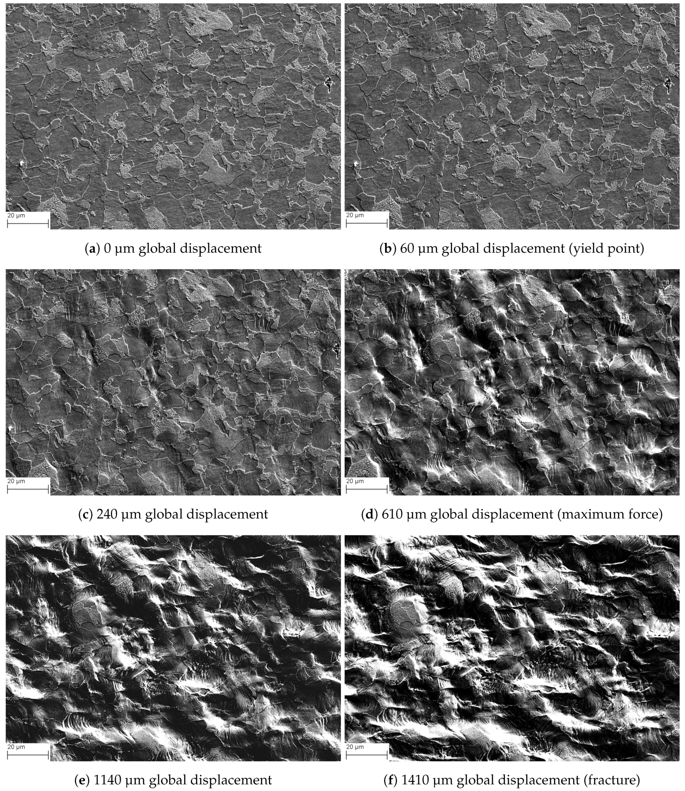
Figure 7 shows the evolution of the microstructure during the tensile test, where Figure 7a reveals the undeformed microstructure. At the yield point (Figure 7b), there is very little difference from the undeformed microstructure, but in Figure 7c it is possible to see that some topography has started to evolve. Slip lines start to appear in Figure 7d, i.e., at the maximum force. More and more slip lines and topography evolution can be seen in Figure 7d–f. During loading, the frames are also getting darker in some areas and whiter in others. This is an effect of the microscope. The reason for the frames getting darker is that the incoming electrons from the SEM contaminates the specimen surface, while the white areas are due to the topography contrast nature of SE imaging.
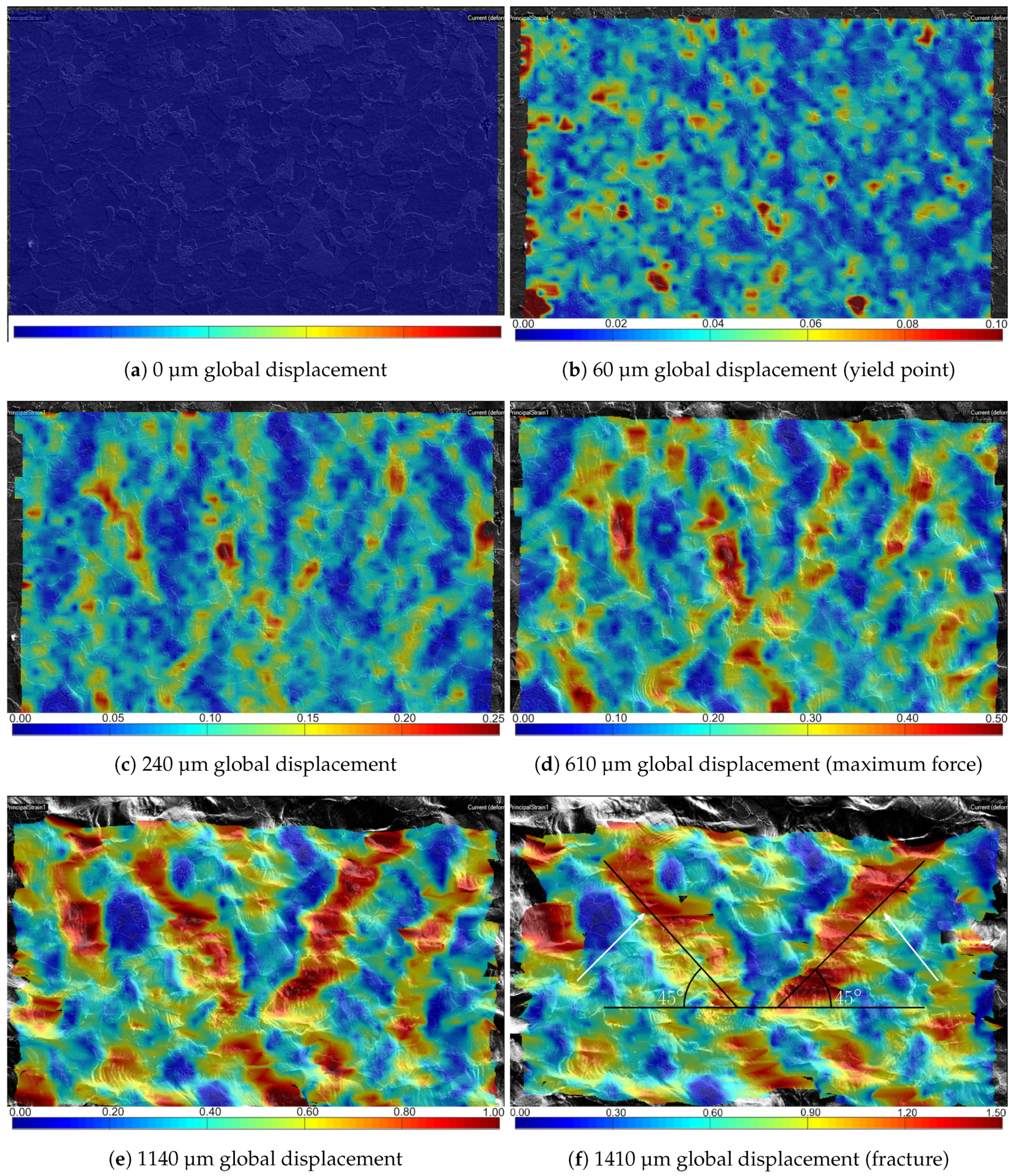
The strain field from the DIC measurements are shown in Figure 8. Here are the same micrographs as in Figure 7, but now with the strain field from the DIC measurements superimposed. When comparing Figure 7 and Figure 8, it is seen that the straining takes place mostly within the soft ferrite, while the hard pearlite appears as less deformed islands within the microstructure. Another observation is that the maximum local strain, measured at element level close to fracture, is more than ε D I C = 2 . 1 . The corresponding average engineering strain across the recorded area was measured to be e ¯ D I C = 0 . 86 , using several virtual extensometers (vectors) in the DIC software with an initial length of 80 µm. The deformation bands seen in Figure 8c–f are oriented at an angle to the tensile direction, and the most heavily deformed bands seem to be oriented at about 45°. This is consistent with the results of, e.g., Ghadbeigi et al. [28]. Initially, the deformation takes place in the soft ferrite, as seen in Figure 8b. Then, bands start to form in Figure 8c during the work-hardening stage. After the formation of these bands, nearly all subsequent deformation takes place inside the localized zones. Next to the heavily deformed bands, there is little deformation. Some places these bands cut through pearlite grains, but for the most part, the less deformed (blue) regions in the strain field are pearlite grains.
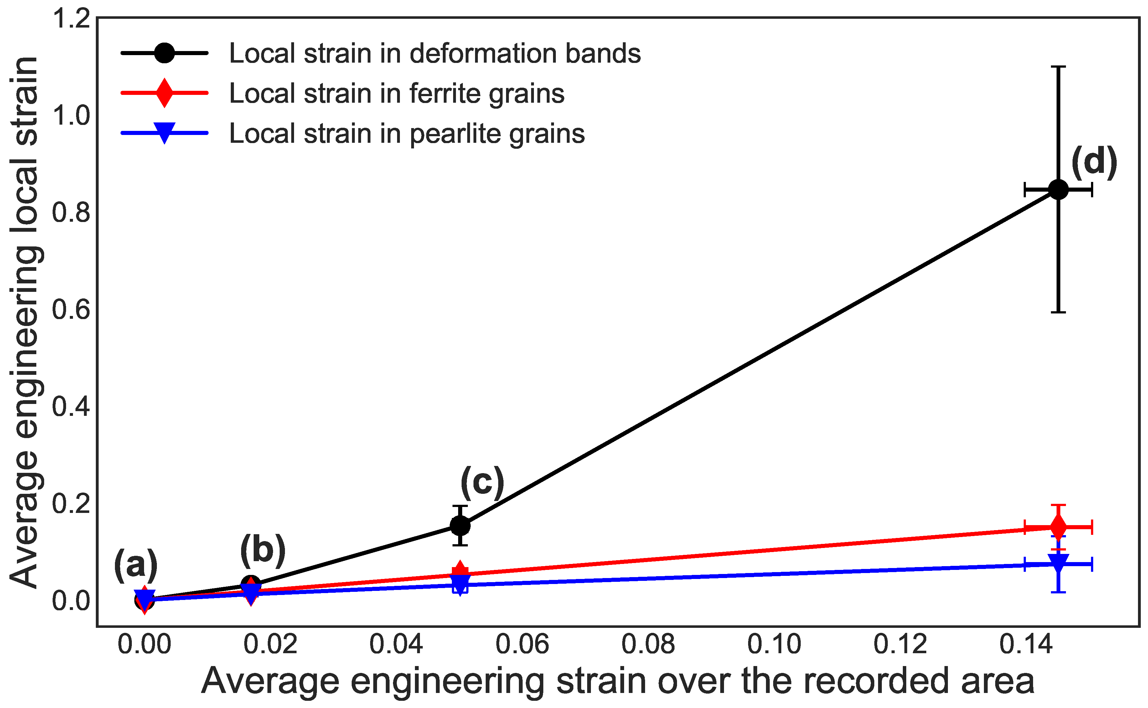
Figure 9 shows the evolution of local engineering strains in pearlite versus ferrite grains as compared to the average engineering strain over the recorded area. As observed on the etched microstructure in Figure 8, the harder pearlite deforms less than the softer ferrite. When e ¯ D I C = 0 . 86 (i.e., the average engineering strain over the recorded area at fracture), the local engineering strain in the pearlite and ferrite grains were e ¯ D I C = 0 . 39 and e ¯ D I C = 0 . 90 , respectively. Both of these strain measures exhibit a rather linear relationship with the average engineering strain over the recorded area, but the spread is significant. In contrast, the heavily deformed bands seem to accommodate more and more of the deformation, especially after the ultimate tensile strength (UTS).
All values in Figure 9 were acquired using virtual extensometers in the DIC software. The grains selected for measuring local strain in ferrite and pearlite are marked in Figure 10a, while the virtual extensometers for the average engineering strain across the recorded area are shown in Figure 10b. In addition, the average value of the local engineering strain across the two deformation bands marked with white arrows in Figure 8f is extracted and plotted in Figure 9. This is done by placing ten virtual extensometers across the length of each band. From this, it is seen that more and more local strain is accumulated in these bands and that the slope of this curve increases with increasing average engineering strain over the recorded area. It is also worth noting that the error bars in Figure 9 represent the standard deviation of the average strains measured and that the amount of variation in the measurements is seen as high.
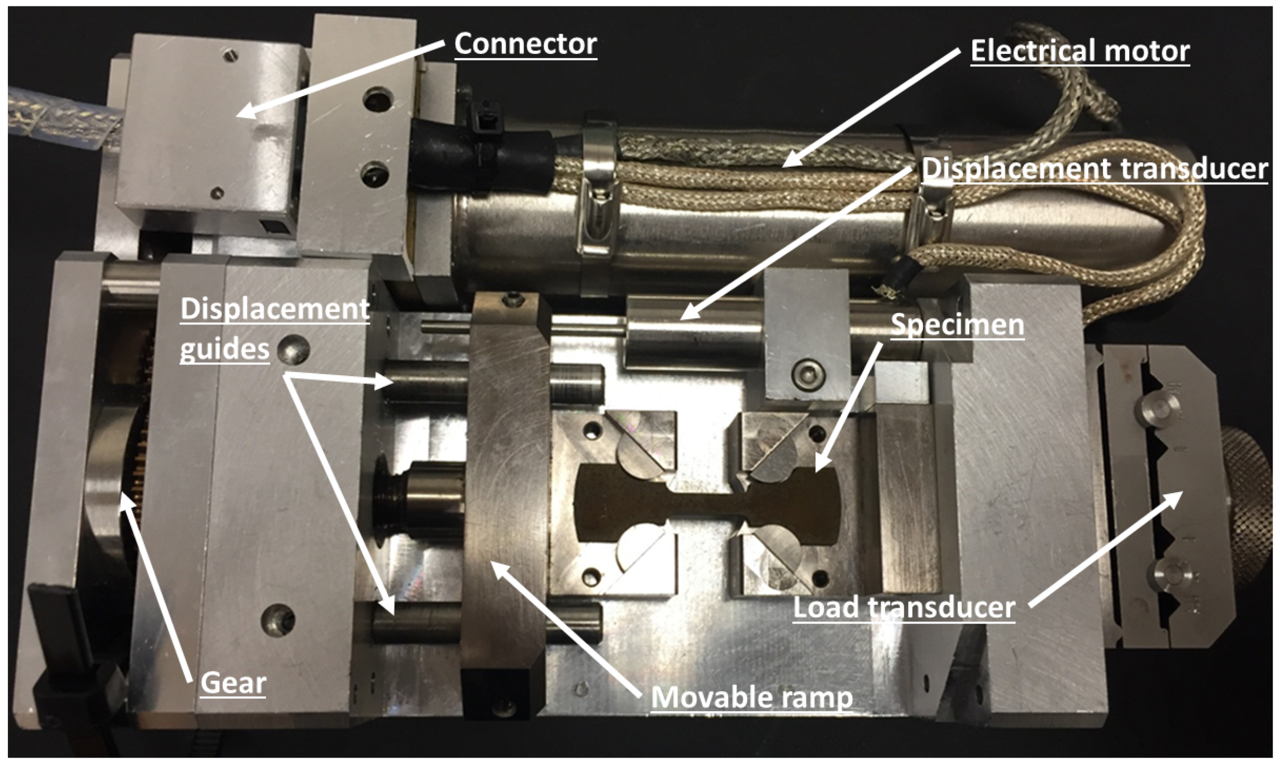
In an attempt to validate the experimental results of the in situ SEM measurements, two types of tests on an unstrained specimen were also conducted. First, a series of images without any pulling was recorded with the same acquisition settings as in the in situ SEM tensile test, before being uploaded to the DIC software and analyzed. Due to the gray-scale pixel noise, a fictitious strain of about 1.5% was registered. This method is similar to the test performed by Buljac et al. [45]. However, they registered an error of 0.3% in a DVC analysis, compared to 1.5% in this DIC analysis. Second, a test with the same setup as in the in situ SEM tensile test, where the specimen was only fixed at one end and then continuously pulled by the movable ramp (see Figure 3), was conducted. This rigid body movement should not impose any strain in the specimen. However, since the microscope loaded the images row-by-row, the last row of pixels was slightly shifted compared to the first row in the image due to the continuous recording. This resulted in a measured constant strain of roughly 3% by the DIC software. These strains are unphysical and should be accounted for. Note that the magnitude of the latter error is a function of exposure time and applied displacement rate during testing, which in this experiment were, respectively, 6 s and 0.2 µm/s.

6. Experimental Results for Gold Speckled Specimen

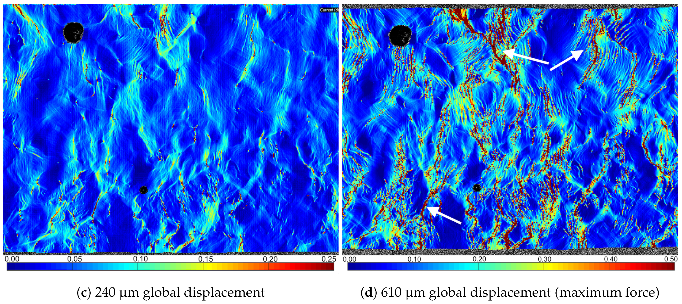
Figure 11 shows the evolution of the microstructure during a tensile test using a gold speckled specimen, where Figure 11a reveals the undeformed microstructure. At the yield point (Figure 11b), there is very little difference from the undeformed microstructure, but in Figure 11c it is possible to see that some slip lines have started to appear. In Figure 11d, i.e., at the maximum force, many slip lines can be seen throughout the microstructure, and the microstructure looks quite deformed. During loading, the frames are also getting darker in a grid pattern. This is an effect of the microscope. The reason for the frames getting darker is that the incoming electrons from the SEM contaminates the specimen surface and it is in a grid pattern since there is an overlapping region being exposed more than the center of each frame. In addition, the middle frame is extra burned due to prolonged exposure between acquisitions.
The DIC results obtained by analyzing the micrographs in Figure 11 are shown in Figure 12. Large parts of the map are unstrained, while some areas are heavily influenced in narrow bands. Figure 13 gives the phase map and the same DIC map as in Figure 12d, but with different scale bar to highlight the undeformed areas. The phase map was created by outlining the NVE36 grains manually from the mapped BSE image. The lamellar structure of NVE36 makes it easy to detect the pearlite and ferrite grains even with the gold coating. By comparing Figure 13a,b, it can be seen that the least strained parts of the microstructure are pearlite grains. In addition, the sharpest bands of strain in the strain field in Figure 12d are in areas near or on the interphase between the two phases. These bands are initially formed at angles close to 45°. Another observation is that the maximum local strain, measured at element level at UTS, is more than ε D I C = 1 . 4 . The corresponding average engineering strain across the recorded area was measured to be e ¯ D I C = 0 . 15 , using several virtual extensometers (vectors) in the DIC software with an initial length of 80 µm.
Figure 14 shows the evolution of local engineering strains in pearlite versus ferrite grains as compared to the average engineering strain over the recorded area. As expected, the hard pearlite deforms much less than the soft ferrite. When e ¯ D I C = 0 . 15 (i.e., the average engineering strain over the recorded area at UTS), the local engineering strain in the pearlite and ferrite grains were e ¯ D I C = 0 . 07 and e ¯ D I C = 0 . 15 , respectively. Both of these strain measures exhibit a rather linear relationship with the average engineering strain over the recorded area, but the spread is significant. All values in Figure 14 were acquired using virtual extensometers in the DIC software. The virtual extensometers for the local engineering strain across the different grains are shown in Figure 15a, while the virtual extensometers for the average engineering strain across the recorded area are shown in Figure 15b.
In addition, the average value of the local engineering strain across the three deformation bands marked with white arrows in Figure 12d is extracted and plotted in Figure 14. In each of the three bands, ten virtual extensometers were placed to measure the average strain across the band. It is shown that more and more local strain is accumulated in these bands and that the slope of this curve increases with increasing average engineering strain over the recorded area.
As for Figure 9, the error bars in Figure 14 represent the standard deviation of the average strains measured and that the amount of variation in the measurements is as seen higher at larger strains. In addition, the spread is greater in the bands compared to the grains. In contrast to Figure 9, Figure 14 is only plotted until UTS. The reason for this is that the gold specimen was only recorded to UTS. The damage and topography beyond this point made it impossible to correlate the DIC results.
The systematic error was calculated by comparing two images from the same region before deformation. These images were then correlated using the DIC software. From this, a peak strain of 1.5% was observed. The error is introduced by the microscope when acquiring BSE images of the speckle pattern by mapping the region of interest (ROI) and stitching the individual frames together. Although there are some nodes in the correlated, undeformed map recording strains of more than 1%, 99.2% of the nodes record strains less than 0.1%.
Further, the gold speckled specimen was analyzed with a mesh size equal (in µm) to the mesh size for the etched specimen. Here, both specimens have a mesh with quadratic element with the size 2.24 µm × 2.24 µm. This corresponds to 280 pixels × 280 pixels and 30 pixels × 30 pixels for the gold speckled specimen and etched specimen, respectively. The resulting strain fields are given in Figure 16, where Figure 16a gives the strain field for the etched specimen and Figure 16b for the gold specimen. Figure 16a is the same strain field as in Figure 8c. It is worth noting that the area for these images is slightly different. The etched specimen has an area of 141 µm × 98 µm and the gold speckled specimen has an area of 114 µm × 85 µm. When comparing the strain maps in Figure 16, the patterns in both maps are similar. The bands in both have the same width and the strain levels are on the same scale. A difference between the two maps is that the strain map from the gold speckled specimen has smoother transitions between the deformed and undeformed areas.

7. Discussion

This work demonstrated that it is possible to correlate a continuously recorded microstructure from an in situ SEM tensile test by DIC using the gray-scale values provided by the micrographs imaged with the SE detector. From this, the strain field can be obtained and related to the evolution of the microstructure all the way to fracture. This technique was compared with a specimen covered with gold nanoparticles, which were used as the speckled pattern for DIC during an in situ SEM tensile test. For the gold speckled specimen, images were acquired using the BSE detector and only at key locations on the tensile curve until UTS. In the present study, these techniques were demonstrated on the ferritic-pearlitic steel NVE36.
The resulting strain fields on the etched specimen obtained are similar to the results achieved by, e.g., Ghadbeigi et al. [28] and Tasan et al. [31], displaying localized deformation bands oriented at about 45° with respect to the loading direction (see Figure 8). These bands follow a path mostly within the soft ferrite grains, reaching local strain values up to 170% before fracture at a much lower global strain, clearly illustrating the heterogeneity in the deformation of the material. This is in line with the observed results by Banerjee et al. [30], who recorded strain values of 150% inside similar bands at a global strain less than 10%. As for the etched specimen, localized deformation bands were observed to form at 45° with respect to the loading direction (see Figure 12) in the gold speckled specimen. This indicates an association with the maximum shear stress locally within grains. Locally, within these bands, strain values of 110% were recorded at UTS, compared to 15% average engineering strain over the recorded area.
When performing the heat treatment to remodel the gold layer in order to obtain a gold speckled pattern, the specimen was kept at 180 °C for 96 h. To validate the effect of this heat treatment, new tensile tests and a microstructural investigation were conducted. The grain size, phase composition, and hardness were all measured before and after heat treatment on three different specimens. The results from these investigations are summarized in Table 3, and it can be seen that all values for both specimens are within the standard deviation of each other. In Figure 17, engineering stress–strain curves from two tensile tests are presented. The curves indicate no difference between the heat-treated tensile curve and the as-received tensile curve. However, this result is not unexpected. The microstructure of NVE36 is decided by the metastable Fe-Fe3C phase diagram (see Figure 9.24 in [46]). As a result, no changes took place in the microstructure during the heat-treating process to remodel the gold layer into the gold speckled pattern for this particular material. Other material can also be considered suitable for this method. These would typically be materials designed for use at elevated temperatures, e.g., nickel alloys, duplex steels, austenitic steels, etc. However, this would not be the case for all materials. As an example, for aluminum alloys, the age hardening might take place at temperatures between 100 °C and 150 °C. If left at 180 °C for 96 h, an overaged material would be the result [47]. In addition, in some cases, tempering of martensite occurs at temperatures of 200 °C [46]. In general, the remodeling method would benefit by reducing the remodeling temperature and remodeling time to increase versatility.
During image acquisition, both the etched specimen and the gold speckled specimen were contaminated by the incoming electrons. In the etched specimen, this results in a gradually darker surface. To overcome this, the reference image in the DIC algorithm was updated several times. The result is an accumulation of errors, as discussed in Tang et al. [35]. For the gold specimen, the contamination resulted in a grid pattern due to the overlapping area during the image acquisition. When studying the overlapping area, it was seen that the intensity of gold speckles are faded. However, from the strain field no apparent changes were observed. The amount of contamination is related to the amount of electrons impacting the surface (i.e., accelerating voltage and aperture size) and absorbed current by the microscope. By reducing the accelerating voltage and aperture size and increasing conductivity between specimen and in situ tensile stage, and in situ tensile stage and microscope stage, the contamination would be reduced.
When studying the strain fields in Figure 8 and the plots in Figure 9, the local strain evolution can be investigated at grain level. The localized deformation initiates in the soft ferrite grains, as seen in Figure 8b. Then, distinct bands of localized strain are formed, which mostly consists of ferrite grains, but occasionally propagate through hard pearlite grains. When the deformation continues to increase, the intensity of the localized strain inside the bands leads to more inhomogeneous plastic flow and unloading of the material outside the bands. In addition, the formation of slip lines was observed, and some of the ferrite grains experienced significant plastic deformation, also activating secondary slip systems. Conversely, some pearlite grains are hardly strained at all having an average engineering strain e ¯ D I C less than 10% at fracture. Figure 8 also confirms that most of the undeformed regions consist of pearlite grains. A few of these grains (situated in the localized strain bands) experienced some slip activity, but no secondary slip systems were observed in this phase. Figure 7 shows the large deformation experienced by the microstructure. From these surface observations, few damage sites were detected, and no void growth could be seen. However, as shown by Maire et al. [48] on dual-phase steel revealing the initiation and growth of damage observed by X-ray microtomography, the void volume fraction is much higher in the center of the specimen where the stress triaxiality is maximum compared to the surface. Such void growth is also well-known from ductile damage mechanics (see, e.g., [49]). This may also explain why the specimen fractured abruptly, with seemingly few damage sites, since a macrocrack might have propagated from below the surface, leading to the final fracture.
In the in situ SEM tensile test with the etched specimen, it was hard to get any meaningful results from the strain maps during the initial stage of the test, i.e., at low strains in the elastic region. This is related to the level of noise in the recorded micrographs. To be able to record a continuous in situ tensile test in the SEM, the exposure time for each micrograph has to be low. Conversely, if the time spent to acquire each micrograph is long compared to the applied displacement rate, the recorded area will move during the imaging. As a result, the final line in the line-scan moved 1.2 µm in the pulling direction compared to the first line. This can, at least to a certain degree, be compensated for with a lower applied displacement rate in the test. In the current experimental set-up, the applied displacement rate was 0.2 µm/s, and the frame rate was 6 s. Thus, the ratio between the applied displacement rate and the frame rate has to be sufficiently low, leaving enough time to acquire good quality micrographs, but high enough to avoid unwanted effects from the low applied displacement rate. In the in situ SEM tensile test on the gold-coated specimen, this issue was resolved by increasing the acquisition time. Here, a snapshot of the current state of the material is seen with slip lines and shear bands forming. Conversely, for the gold speckled specimen, high-quality images were acquired at the desired strain level. The resulting DIC maps achieve an excellent spatial resolution, but the image acquisition time is long. As a result, a strain map was not obtained throughout the tensile test, but at a few selected locations on the tensile curve. In addition, the images acquired for the gold speckled specimen were acquired by mapping the surface frame by frame and then stitching all frames into the ROI. To obtain the best results possible, a very precise stage is required. Ideally, this should be a piezoelectric stage as they have superior precision when the stage moves between each frame acquired. The mechanical stage used here has a precision of 1 µm. However, new piezoelectric stages are 500–1000 times more precise [50].
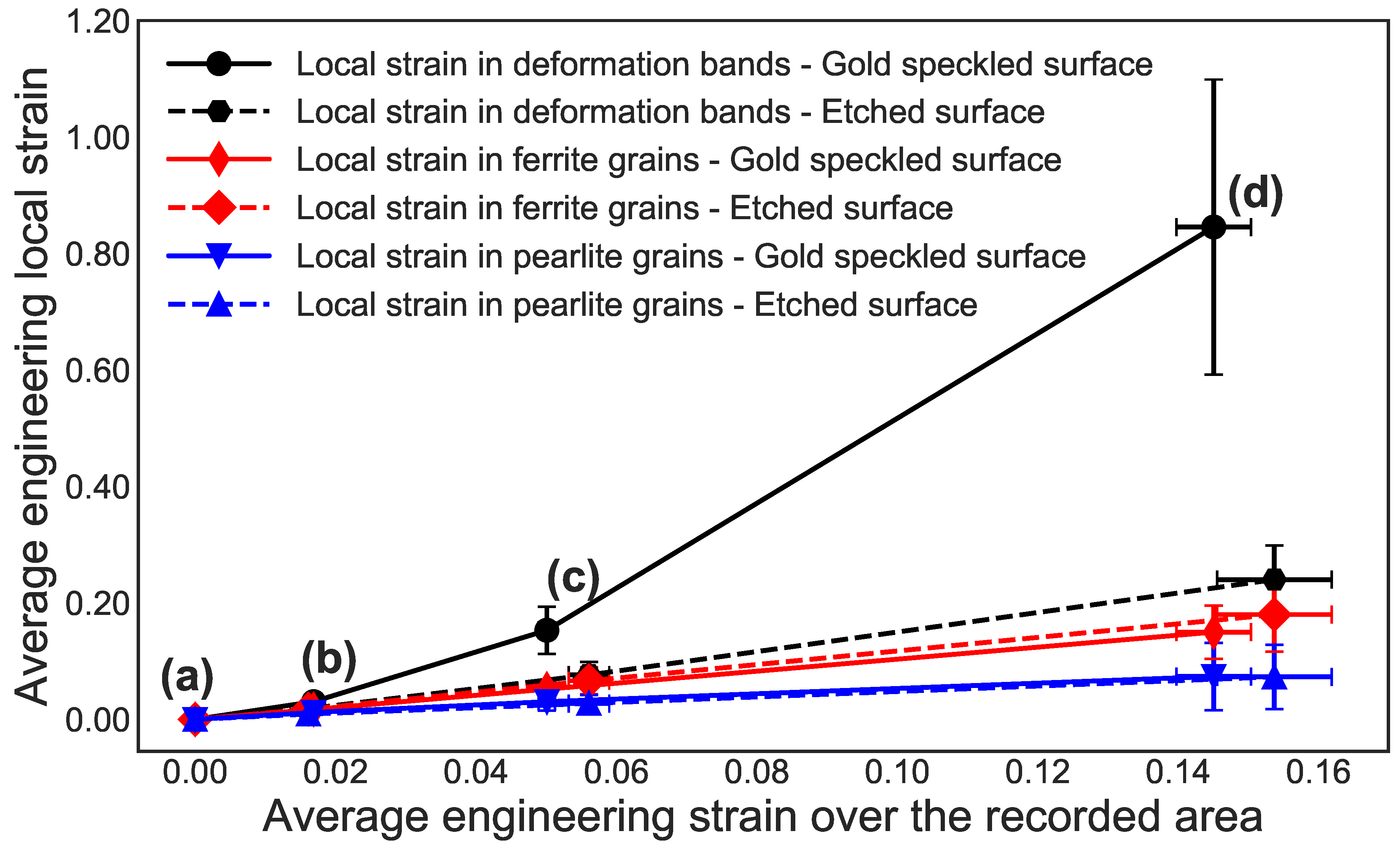
Figure 18 compares the local strain evolution of techniques used on the specimens tested here. It can be seen that the behavior of the grains and local average strain for both techniques captures the same behavior for the pearlite and ferrite grains. However, in the deformation bands, there is a clear difference. The maximum principal strain at UTS was found to be 325% higher in the gold speckled specimen than in the etched specimen. Haltom et al. [51] reported similar differences based on microscopic and macroscopic strain measurements in an aluminum alloy. From the in situ SEM strain maps, it is readily observed where and in which type of grain strain localization takes place, and at what time this occurs during the deformation process. It is also straightforward to relate these measurements to the applied force or stress magnitude. Moreover, the technique can be further developed by investigating other materials, such as quasi-brittle alloys at various temperatures where fracture is essential.

8. Concluding Remarks

In this study, the differences between two specimen preparation methods for DIC on images acquired in an SEM have been demonstrated on the two-phased ferritic-pearlitic steel NVE36. The gold speckled specimen has a significantly higher spatial resolution, and, as a consequence, more local deformation is captured. In addition, if local information is required at the early stages of deformation, the gold speckled specimen is the preferred method. Conversely, the images from the etched specimen surface contain more noise, and in the first stages of deformation less local information is captured. As a consequence of the lack of contrast for the DIC analysis, the etched specimen is not able to resolve strains within grains. However, the advantages of using an etched surface are that no heating of the specimen and fewer steps are required to obtain the strain field. In addition, continuous recordings of the strain field are particularly important when studying localization and fracture, which may occur abruptly. As a conclusion, the method with gold speckles is only required when a fine spatial resolution is necessary to obtain results at only certain stages of the tensile curve.
The gold speckled specimen gives more detail and higher accuracy compared to the etched specimen. Local strain bands are found to be more narrow and more heavily deformed using this approach. However, with the gold speckled specimen, only a few snapshots throughout the tensile test are acquired, and after UTS the topography on the surface makes the image acquisition more challenging. This is a consequence of acquiring BSE images. For the etched specimen, images are captured continuously through the test. When performing a DIC analysis on the gold speckled specimen with a mesh size (in µm) equal to the etched specimen, the results are close to identical. The differences between the two techniques are specimen preparation, image acquisition, acquisition time, DIC quality, DIC resolution, and the number of strain fields available throughout the stress–strain curve. The technique to be chosen will mainly depend on the material, and the spatial resolution required.

Author Contributions

C.O.P. is the first author and analyzed the data, wrote most of the paper, and performed the experiments. E.F. contributed to the DIC parts of the paper. He helped to perform the DIC analysis, writing the section on DIC and is the DIC expert. I.W. and T.B. conceived, designed, and supervised the experiments. In addition, they contributed to the interpretation of data and editing the paper.

Funding

The authors gratefully appreciate the financial support from NTNU and the Research Council of Norway through CASA, Project No. 237885.

Conflicts of Interest

The authors declare no conflict of interest.

Abbreviations

The following abbreviations are used in this manuscript:
BSEBackscatter Electron
CASACentre for Advanced Structural Analysis
DICDigital Image Correlation
DOFDegrees of Freedom
EBSDElectron Backscatter Diffraction
FEFinite Element
NTNUNorwegian University of Science and Technology
ROIRegion of Interest
SESecondary Electron
SEMScanning Electron Microscope
SIMLabStructural Impact Laboratory
UTSUltimate Tensile Strength
ZNSSDZero-Mean Normalized Sum of Squared Differences

References

  1. Bhadeshia, H.; Honeycombe, R. Thermomechanical Treatment of Steels. In Steels: Microstructure and Properties; Elsevier: Oxford, UK, 2017; pp. 271–301. [Google Scholar] [CrossRef]
  2. Dieter, G.E.; Bacon, D.J. Mechanical Metallurgy; McGraw-Hill: New York, NY, USA, 1988; Volume 3. [Google Scholar]
  3. Porter, D.A.; Easterling, K.E.; Smith, G.D.W. Dynamic studies of the tensile deformation and fracture of pearlite. Acta Metall. 1978, 26, 1405–1422. [Google Scholar] [CrossRef]
  4. Sidhom, H.; Yahyaoui, H.; Braham, C.; Gonzalez, G. Analysis of the Deformation and Damage Mechanisms of Pearlitic Steel by EBSD and in-situ SEM Tensile Tests. J. Mater. Eng. Perform. 2015, 24, 2586–2596. [Google Scholar] [CrossRef]
  5. Peters, W.H.; Ranson, W.F. Digital Imaging Techniques In Experimental Stress Analysis. Opt. Eng. 1982, 21, 427–432. [Google Scholar] [CrossRef]
  6. Sutton, M.A.; Wolters, W.J.; Peters, W.H.; Ranson, W.F.; McNeill, S.R. Determination of displacements using an improved digital correlation method. Image Vis. Comput. 1983, 1, 133–139. [Google Scholar] [CrossRef]
  7. Sutton, M.A.; Mingqi, C.; Peters, W.H.; Chao, Y.J.; McNeill, S.R. Application of an optimized digital correlation method to planar deformation analysis. Image Vis. Comput. 1986, 4, 143–150. [Google Scholar] [CrossRef]
  8. Sutton, M.A.; Turner, J.L.; Bruck, H.A.; Chae, T.A. Full-field representation of discretely sampled surface deformation for displacement and strain analysis. Exp. Mech. 1991, 31, 168–177. [Google Scholar] [CrossRef]
  9. Bruck, H.A.; McNeill, S.R.; Sutton, M.A.; Peters, W.H. Digital image correlation using Newton-Raphson method of partial differential correction. Exp. Mech. 1989, 29, 261–267. [Google Scholar] [CrossRef]
  10. Besnard, G.; Hild, F.; Roux, S. “Finite-element” displacement fields analysis from digital images: Application to Portevin-Le Châtelier bands. Exp. Mech. 2006, 46, 789–803. [Google Scholar] [CrossRef]
  11. Réthoré, J.; Roux, S.; Hild, F. From pictures to extended finite elements: extended digital image correlation (X-DIC). C. R.-Mec. 2007, 335, 131–137. [Google Scholar] [CrossRef] [Green Version]
  12. Réthoré, J.; Hild, F.; Roux, S. Extended digital image correlation with crack shape optimization. Int. J. Numer. Methods Eng. 2008, 73, 248–272. [Google Scholar] [CrossRef]
  13. Fagerholt, E.; Børvik, T.; Hopperstad, O. Measuring discontinuous displacement fields in cracked specimens using digital image correlation with mesh adaptation and crack-path optimization. Opt. Lasers Eng. 2013, 51, 299–310. [Google Scholar] [CrossRef]
  14. Schreier, H.; Orteu, J.J.; Sutton, M.A. Image Correlation for Shape, Motion and Deformation Measurements: Basic Concepts, Theory and Applications; Springer: London, UK, 2009. [Google Scholar] [CrossRef]
  15. Kang, J.; Ososkov, Y.; Embury, J.D.; Wilkinson, D.S. Digital image correlation studies for microscopic strain distribution and damage in dual phase steels. Scr. Mater. 2007, 56, 999–1002. [Google Scholar] [CrossRef]
  16. Di Gioacchino, F.; Quinta da Fonseca, J. Plastic Strain Mapping with Sub-micron Resolution Using Digital Image Correlation. Exp. Mech. 2013, 53, 743–754. [Google Scholar] [CrossRef]
  17. Quinta da Fonseca, J.; Ko, L. The kinematics of deformation and the development of substructure in the particle deformation zone. In IOP Conference Series: Materials Science and Engineering; IOP Publishing: Bristol, UK, 2015; Volume 89, p. 012012. [Google Scholar] [CrossRef]
  18. Orozco-Caballero, A.; Lunt, D.; Robson, J.D.; Quinta da Fonseca, J. How magnesium accommodates local deformation incompatibility: A high-resolution digital image correlation study. Acta Mater. 2017, 133, 367–379. [Google Scholar] [CrossRef]
  19. Polatidis, E.; Hsu, W.N.; Šmíd, M.; Van Swygenhoven, H. A High Resolution Digital Image Correlation Study under Multiaxial Loading. Exp. Mech. 2018, 59, 309–317. [Google Scholar] [CrossRef] [Green Version]
  20. Lunt, D.; Orozco-Caballero, A.; Thomas, R.; Honniball, P.; Frankel, P.; Preuss, M.; Quinta da Fonseca, J. Enabling high resolution strain mapping in zirconium alloys. Mater. Charact. 2018, 139, 355–363. [Google Scholar] [CrossRef]
  21. Allais, L.; Bornert, M.; Bretheau, T.; Caldemaison, D. Experimental characterization of the local strain field in a heterogeneous elastoplastic material. Acta Metall. Mater. 1994, 42, 3865–3880. [Google Scholar] [CrossRef]
  22. Ishikawa, N.; Yasuda, K.; Sueyoshi, H.; Endo, S.; Ikeda, H.; Morikawa, T.; Higashida, K. Microscopic deformation and strain hardening analysis of ferrite-bainite dual-phase steels using micro-grid method. Acta Mater. 2015, 97, 257–268. [Google Scholar] [CrossRef]
  23. Latourte, F.; Salez, T.; Guery, A.; Rupin, N.; Mahé, M. Deformation studies from in situ SEM experiments of a reactor pressure vessel steel at room and low temperatures. J. Nucl. Mater. 2014, 454, 373–380. [Google Scholar] [CrossRef]
  24. Lagattu, F.; Bridier, F.; Villechaise, P.; Brillaud, J. In-plane strain measurements on a microscopic scale by coupling digital image correlation and an in situ SEM technique. Mater. Charact. 2006, 56, 10–18. [Google Scholar] [CrossRef]
  25. Ososkov, Y.; Wilkinson, D.S.; Jain, M.; Simpson, T. In-situ measurement of local strain partitioning in a commercial dual-phase steel. Int. J. Mater. Res. 2007, 98, 664–673. [Google Scholar] [CrossRef]
  26. Kang, J.; Wilkinson, D.S.; Embury, J.D.; Jain, M. Microscopic Strain Mapping Using Scanning Electron Microscopy Topography Image Correlation at Large Strain. J. Strain Anal. Eng. Des. 2005, 40, 559–570. [Google Scholar] [CrossRef]
  27. Ghadbeigi, H.; Pinna, C.; Celotto, S. Quantitative Strain Analysis of the Large Deformation at the Scale of Microstructure: Comparison between Digital Image Correlation and Microgrid Techniques. Exp. Mech. 2012, 52, 1483–1492. [Google Scholar] [CrossRef] [Green Version]
  28. Ghadbeigi, H.; Pinna, C.; Celotto, S.; Yates, J.R. Local plastic strain evolution in a high strength dual-phase steel. Mater. Sci. Eng. A 2010, 527, 5026–5032. [Google Scholar] [CrossRef]
  29. Kapp, M.; Hebesberger, T.; Kolednik, O. A micro-level strain analysis of a high-strength dual-phase steel. Int. J. Mater. Res. 2011, 102, 687–691. [Google Scholar] [CrossRef]
  30. Banerjee, S.; Dasgupta, T.; Mukherjee, S.; Shome, M.; Chakraborti, P.C.; Saha, S.K. Digital image correlation for grain scale strain measurement in interstitial free high strength steel. Mater. Sci. Technol. 2016, 32, 328–337. [Google Scholar] [CrossRef]
  31. Tasan, C.C.; Hoefnagels, J.P.M.; Geers, M.G.D. Microstructural banding effects clarified through micrographic digital image correlation. Scr. Mater. 2010, 62, 835–838. [Google Scholar] [CrossRef]
  32. Lindfeldt, E.; Ekh, M.; Cvetskovski, K.; Schilke, M. Using DIC to Identify Microscale Strain Fields from In-situ SEM Images of a Pearlitic Steel. Exp. Mech. 2014, 54, 1503–1513. [Google Scholar] [CrossRef]
  33. DNV. Newbuildings Materials and Welding-Metallic Materials. Available online: https://rules.dnvgl.com/docs/pdf/DNV/rulesship/2011-01/ts202.pdf (accessed on 20 June 2019).
  34. Fagerholt, E. Field Measurements in Mechanical Testing Using Close-Range Photogrammetry and Digital Image Analysis. Ph.D. Thesis, Norwegian University of Science and Technology, Trondheim, Norway, 2012. Available online: http://folk.ntnu.no/egilf/Thesis_Egil_Fagerholt.pdf (accessed on 20 June 2019).
  35. Tang, Z.; Liang, J.; Xiao, Z.; Guo, C. Large deformation measurement scheme for 3D digital image correlation method. Opt. Lasers Eng. 2012, 50, 122–130. [Google Scholar] [CrossRef]
  36. Hild, F.; Raka, B.; Baudequin, M.; Roux, S.; Cantelaube, F. Multiscale displacement field measurements of compressed mineral-wool samples by digital image correlation. Appl. Opt. 2002, 41, 6815–6828. [Google Scholar] [CrossRef]
  37. Holzapfel, G.A. Nonlinear Solid Mechanics: A Continuum Approach for Engineering; John Wiley and Sons Ltd.: Hoboken, NJ, USA, 2000. [Google Scholar]
  38. Karlsen, M.; Hjelen, J.; Grong, Ø.; Rørvik, G.; Chiron, R.; Schubert, U.; Nilsen, E. SEM/EBSD based in situ studies of deformation induced phase transformations in supermartensitic stainless steels. Mater. Sci. Technol. 2008, 24, 64–72. [Google Scholar] [CrossRef]
  39. Karlsen, M.; Grong, Ø.; Søfferud, M.; Hjelen, J.; Rørvik, G.; Chiron, R. Scanning electron microscopy/electron backscatter diffraction—Based observations of martensite variant selection and slip plane activity in supermartensitic stainless steels during plastic deformation at elevated, ambient, and subzero temperatures. Metall. Mater. Trans. A: Phys. Metall. Mater. Sci. 2009, 40, 310–320. [Google Scholar] [CrossRef]
  40. Paulsen, C.; Broks, R.; Karlsen, M.; Hjelen, J.; Westermann, I. Microstructure Evolution in Super Duplex Stainless Steels Containing σ-Phase Investigated at Low-Temperature Using In Situ SEM/EBSD Tensile Testing. Metals 2018, 8, 478. [Google Scholar] [CrossRef]
  41. Fagerholt, E. Ecorr User Manual. Available online: http://folk.ntnu.no/egilf/ecorr/doc/ (accessed on 20 June 2019).
  42. Schindelin, J.; Arganda-Carreras, I.; Frise, E.; Kaynig, V.; Longair, M.; Pietzsch, T.; Preibisch, S.; Rueden, C.; Saalfeld, S.; Schmid, B.; et al. Fiji: An open-source platform for biological-image analysis. Nat. Methods 2012, 9, 676–682. [Google Scholar] [CrossRef] [PubMed]
  43. Preibisch, S.; Saalfeld, S.; Tomancak, P. Globally optimal stitching of tiled 3D microscopic image acquisitions. Bioinformatics 2009, 25, 1463–1465. [Google Scholar] [CrossRef] [PubMed]
  44. Schneider, C.A.; Rasband, W.S.; Eliceiri, K.W. NIH Image to ImageJ: 25 years of image analysis. Nat. Methods 2012, 9, 671–675. [Google Scholar] [CrossRef]
  45. Buljac, A.; Hild, F.; Helfen, L.; Morgeneyer, T.F. On deformation and damage micromechanisms in strong work hardening 2198 T3 aluminium alloy. Acta Mater. 2018, 149, 29–45. [Google Scholar] [CrossRef] [Green Version]
  46. Callister, W.; Rethwisch, D. Materials Science and Engineering: An Introduction, 7th ed.; John Wiley & Sons: Hoboken, NJ, USA, 2007; p. 290. [Google Scholar]
  47. Westermann, I.; Hopperstad, O.S.; Marthinsen, K.; Holmedal, B. Ageing and work-hardening behaviour of a commercial AA7108 aluminium alloy. Mater. Sci. Eng. A 2009, 524, 151–157. [Google Scholar] [CrossRef]
  48. Maire, E.; Bouaziz, O.; Di Michiel, M.; Verdu, C. Initiation and growth of damage in a dual-phase steel observed by X-ray microtomography. Acta Mater. 2008, 56, 4954–4964. [Google Scholar] [CrossRef]
  49. Anderson, T.L. Solutions Manual: Fracture Mechanics: Fundamentals and Applications; CRC Press: Boca Raton, FL, USA, 1995. [Google Scholar]
  50. Kleindiek Nanotechnik. LT12830 Substage. Available online: https://www.kleindiek.com/fileadmin/public/brochures/lt12830.pdf (accessed on 20 June 2019).
  51. Haltom, S.S.; Kyriakides, S.; Ravi-Chandar, K. Ductile failure under combined shear and tension. Int. J. Solids Struct. 2013, 50, 1507–1522. [Google Scholar] [CrossRef]
Figure 1. Secondary electron image of the undeformed microstructure. The darker areas are ferrite grains and the lighter areas are pearlite grains.Micrograph of NVE36
Metals 09 00820 g001
Figure 2. (a) This figure shows how the specimens are taken from the NVE36 plate. The plate and specimen are not in scale. (b) The notched specimen geometry used for in situ SEM tensile tests. All measurements are in mm.
Metals 09 00820 g002
Figure 3. Image showing the in situ SEM tensile test device.
Metals 09 00820 g003
Figure 4. Area observed during the two in situ SEM tensile tests. The red square has the dimensions 160 µm × 120 µm and is from the test on the etched specimen.
Metals 09 00820 g004
Figure 5. Experimental setup for gold remodeling in an argon/styrene atmosphere. Argon gas flows into a gas washing bottle filled with styrene. From here, a mixture of argon and styrene is guided into a remodeling chamber placed inside a desiccator. Inside the remodeling chamber, the specimen is placed on top of a hot plate. The control box sets the temperature of the hot plate on the outside of the desiccator.
Metals 09 00820 g005
Figure 6. Measured force–displacement curve for the etched specimen during an in situ SEM tensile test. The labels (af) are related to the micrographs in Figure 7 and Figure 8.
Metals 09 00820 g006
Figure 7. Micrographs at different displacements in the etched specimen. (af) The micrographs relate to the force–displacement curve in Figure 6. In all frames, the pulling direction in the in situ SEM tensile test is from right to left. Each frame has the same dimensions, 160 µm × 108 µm.
Metals 09 00820 g007
Figure 8. Micrographs with the measured strain field superimposed at different global displacements in the notched specimen. (af) The strain maps relate to the force–displacement curve in Figure 6. The white arrows in (f) indicate the deformation bands discussed in Figure 9. In all frames, the pulling direction in the in situ SEM tensile test is from right to left. Each frame has the same dimension, 160 µm × 108 µm. The fringe colors give values of the major principle strain.
Metals 09 00820 g008
Figure 9. Local strain evolution in pearlite and ferrite grains and the localized deformation bands marked in Figure 8f. The grains selected for the local strain measurements are indicated with blue squares and red diamonds in Figure 10a for pearlite and ferrite, respectively. The average engineering strain over the recorded area are measured using the vectors in Figure 10b.
Metals 09 00820 g009
Figure 10. (a) Grains used for local strain measurements in Figure 9, where the blue squares are pearlite grains and the red diamonds are ferrite grains. (b) Vectors used as virtual extensometer for the average engineering strain over the recorded area, having an initial length of 80 µm.
Metals 09 00820 g010
Figure 11. Stitched BSE images at different displacements in the notched specimen. (ad) The micrographs relate to the force–displacement curve in Figure 6. In all frames, the pulling direction in the in situ SEM tensile test is from right to left. Each frame has the same dimensions, 119 µm × 90 µm.
Metals 09 00820 g011
Figure 12. Measured strain field superimposed on the BSE images from Figure 11 at different global displacements in the notched specimen. (ad) The strain maps relate to the force–displacement curve in Figure 6. The white arrows in (d) indicate the deformation bands discussed in Figure 14. In all frames, the pulling direction in the in situ SEM tensile test is from right to left. Each frame has the same dimensions, 119 µm × 90 µm. The fringe colors give values of the major principle strain.
Metals 09 00820 g012aMetals 09 00820 g012b
Figure 13. (a) A phase map of the same area as analyzed with DIC. The pearlitic phase is black and ferrite is white. (b) The same strain map as in Figure 12d with a lower max value for the color legend.
Metals 09 00820 g013
Figure 14. Local strain evolution in pearlite and ferrite grains and the localized deformation bands marked in Figure 12d. The grains selected for the local strain measurements are indicated with blue squares and red diamonds in Figure 15a for pearlite and ferrite, respectively. The average engineering strain over the recorded area are measured using the vectors in Figure 15b.
Metals 09 00820 g014
Figure 15. (a) Grains used for local strain measurements in Figure 14, where the blue squares are pearlite grains and the red diamonds are ferrite grains. (b) Vectors used as virtual extensometer for the average engineering strain over the recorded area, having an initial length of 80 µm.
Metals 09 00820 g015
Figure 16. Comparing the two techniques when having the same mesh size (in µm): (a) etched specimen with an area of 141 µm × 98 µm; and (b) gold speckled specimen with an area of 114 µm × 85 µm.
Metals 09 00820 g016
Figure 17. The tensile test curve of the heat treated and as received specimen.
Metals 09 00820 g017
Figure 18. The local strain evolution in Figure 9 and Figure 14 plotted together until UTS.
Metals 09 00820 g018
Table 1. Typical chemical composition of NVE36 (wt.%) [33].
ElementCSiMnPSCrMoNiCuAlNbVTi
Content0.180.50.9–1.60.0350.0350.20.080.40.350.020.030.050.01
Table 2. Settings used when coating the specimen with gold.
ParameterSetting
Current [mA]40
Voltage [kV]0.5
Time [min]3–4
Pressure [mbar]7.8
Table 3. Hardness, grain size and phase composition measured before and after heat treatment.
VariableFerritePearliteFerritePearlite
BeforeAfter
Phase composition75 ± 19% ferrite74 ± 16% ferrite
Hardness [HV]204 ± 23283 ± 27188 ± 29306 ± 39
Grain size [µm]15.5 ± 3.112 ± 2.116 ± 2.511 ± 1.1

