Review

3D Printing of Highly Pure Copper

1
Department of Mechanical Engineering, National University of Singapore, 9 Engineering Drive 1, EA-07-05, Singapore 117575, Singapore
2
Faculty of Mechanical Engineering, Ho Chi Minh City University of Technology, VNUHCM, 268 Ly Thuong Kiet, District 10, Ho Chi Minh City 740400, Vietnam
3
Institute of Materials Engineering, National Laboratory of Solid State Microstructures, College of Engineering and Applied Sciences, Nanjing University, Nanjing 210093, China
4
Lightweight Materials Laboratory, Department of Mechanical Engineering, National Institute of Technology Karnataka, Surathkal 575025, India
*
Authors to whom correspondence should be addressed.
Metals 2019, 9(7), 756; https://doi.org/10.3390/met9070756
Submission received: 14 June 2019 / Revised: 29 June 2019 / Accepted: 2 July 2019 / Published: 5 July 2019

Abstract

:
Copper has been widely used in many applications due to its outstanding properties such as malleability, high corrosion resistance, and excellent electrical and thermal conductivities. While 3D printing can offer many advantages from layer-by-layer fabrication, the 3D printing of highly pure copper is still challenging due to the thermal issues caused by copper’s high conductivity. This paper presents a comprehensive review of recent work on 3D printing technology of highly pure copper over the past few years. The advantages and current issues of 3D printing methods are compared while different properties of copper parts printed by these methods are summarized. Finally, we provide several potential applications of the 3D printed copper parts and an overview of current developments that could lead to new improvements in this advanced manufacturing field.

1. Introduction

During the last decades, 3D printing of metallic parts directly from 3D computer-aided design (CAD) models has drawn significant attention from both academia and industry [1,2,3,4,5,6]. One of the important advantages of 3D printing is the higher design freedom compared to conventional fabrication technologies [7,8,9,10]. In fact, complex 3D parts such as components with many internal structures or cellular parts can be fabricated by 3D printing without considering specific design rules. Moreover, the topological optimization of 3D CAD models with no additional cost in 3D printing provides many advantages such as complex shapes, short lead times, weight saving, and multifunctional integration [11]. Nowadays, many high-performance metallic alloys and pure metals can be processed successfully with achievable properties comparable to those fabricated by conventional methods such as forming or casting [1,2,3,4]. Additionally, parts with epitaxial growth and fine microstructures can be fabricated by process-inherent rapid and direct solidification in 3D printing. This offers a great potential in new design possibilities to achieve locally-desired material properties. Besides, the application of high cooling rates during 3D printing processes provides new possibilities in alloy and metal design [1,2,3,4].
3D printing of highly pure copper with superior electrical and thermal properties has been studied extensively due to its broad potential in many applications including electronic devices [1,12,13,14,15,16,17,18,19,20], thermal management systems [4,12], and the aerospace industry [4,12,21,22,23,24,25]. Compared to conventional fabrication methods such as metal casting, welding, and machining, 3D printing can fabricate more optimized and complex 3D copper parts without using additional tools [26,27,28,29,30,31,32,33,34]. Post-processing methods such as abrasive polishing [35] and hot isostatic pressing (HIP) [36,37,38,39] could enhance physical properties of the printed copper parts further. However, 3D printing of pure copper has several significant processing challenges that need to be addressed. Due to copper’s high thermal conductivity, the melt area experiences rapid heat dissipation and high local thermal gradients, resulting in delamination, layer curling, and part failure [40,41]. Furthermore, the post-build powder removal and recovery of the printed parts might be impeded by the high ductility of copper while the tendency of powder agglomeration could lower overall flowability and hinder powder deposition. Additionally, special handling and storage of copper are required for 3D printing processes due to the high sensitivity of copper to oxidation [40,41,42].
Although many papers have been published on 3D printing of highly pure copper [12,21,26,40,43], no comprehensive review has been reported. Recent rapid growth in research on the 3D printing of pure copper has motivated this review. In Section 2, we present the main 3D printing methods for pure copper over the past few years. The advantages and challenges of each 3D printing method are discussed in Section 3. In Section 4, the potential applications of 3D printed copper parts are summarized, and a brief conclusion is presented in Section 5.

2. 3D Printing Methods of Highly Pure Copper

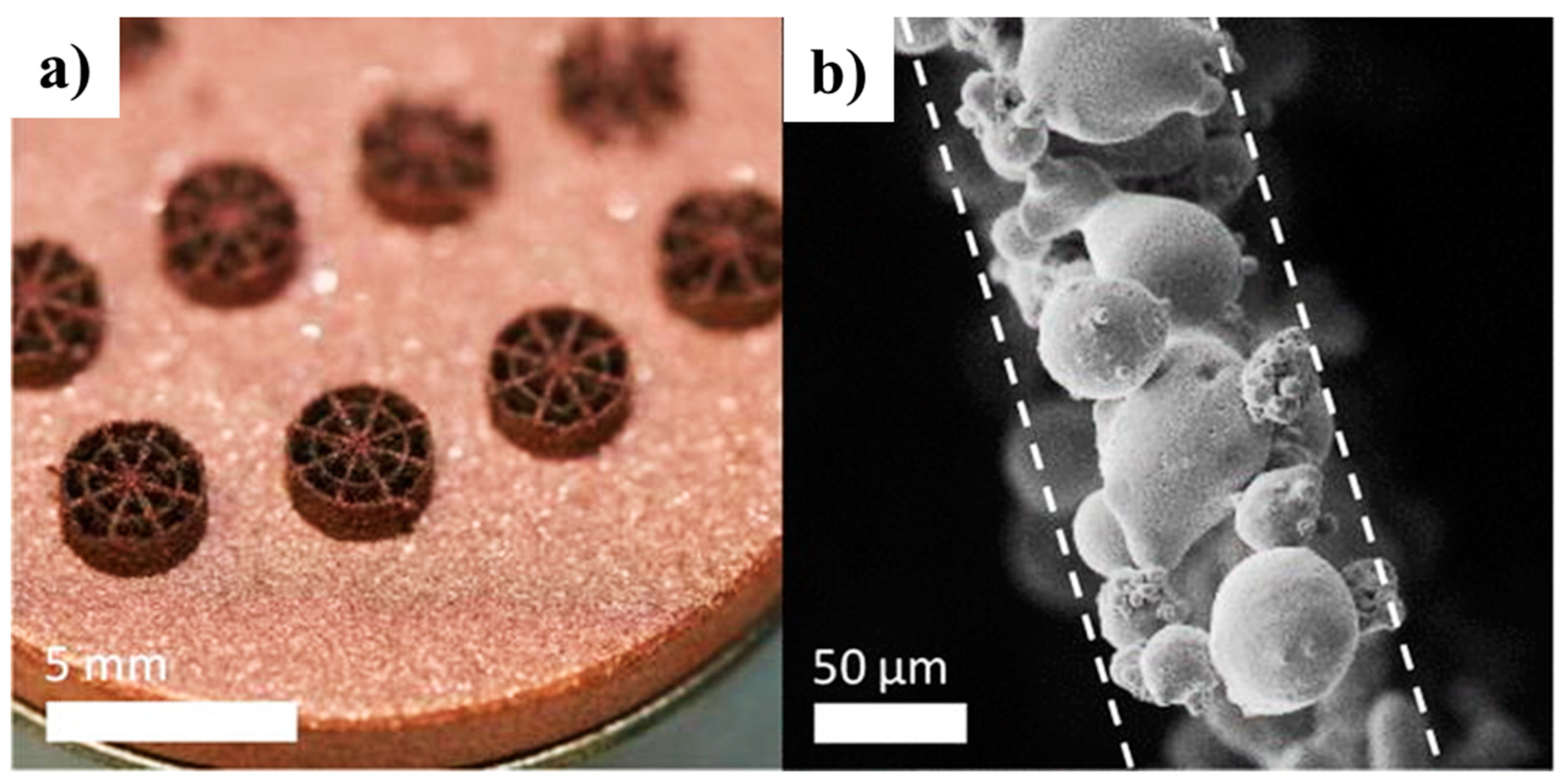
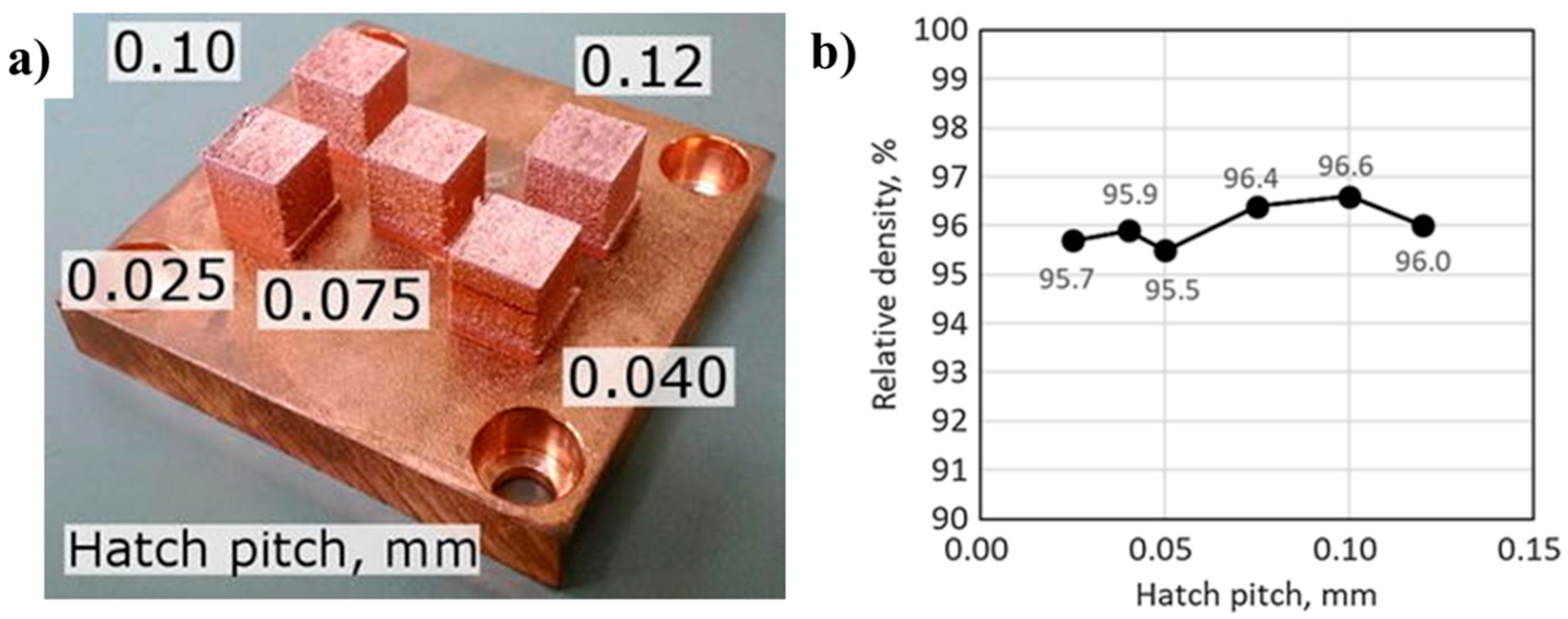
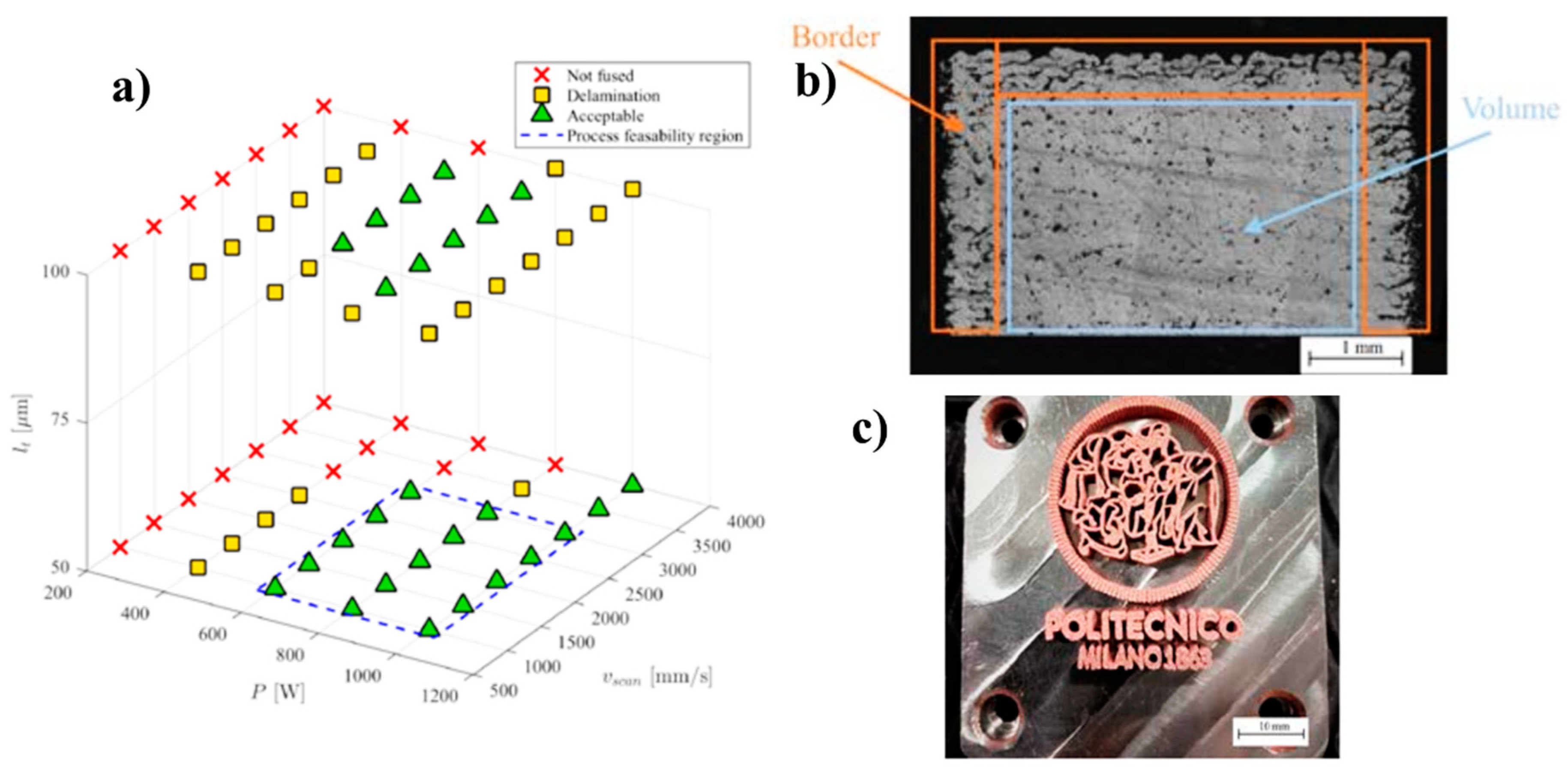
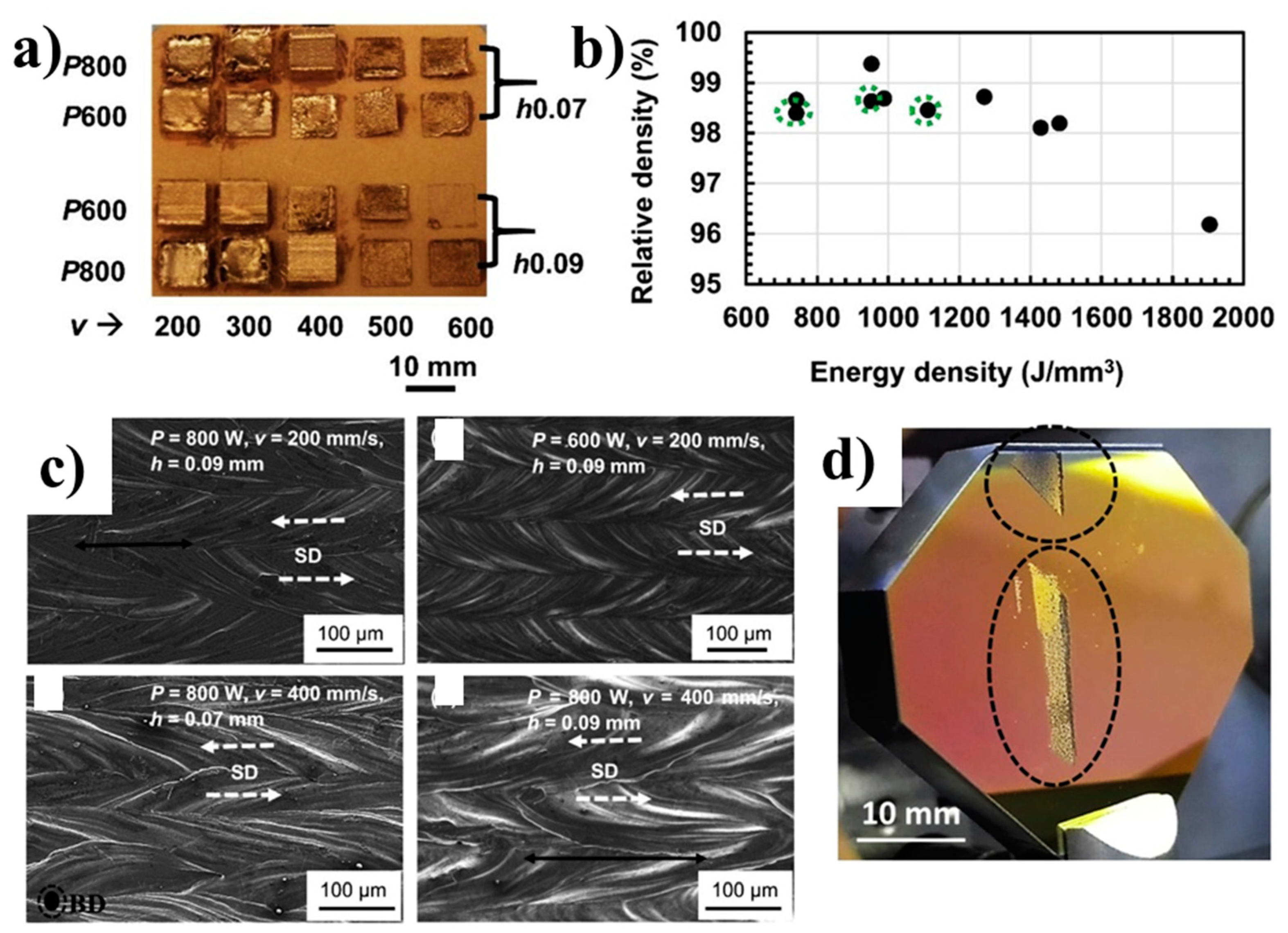
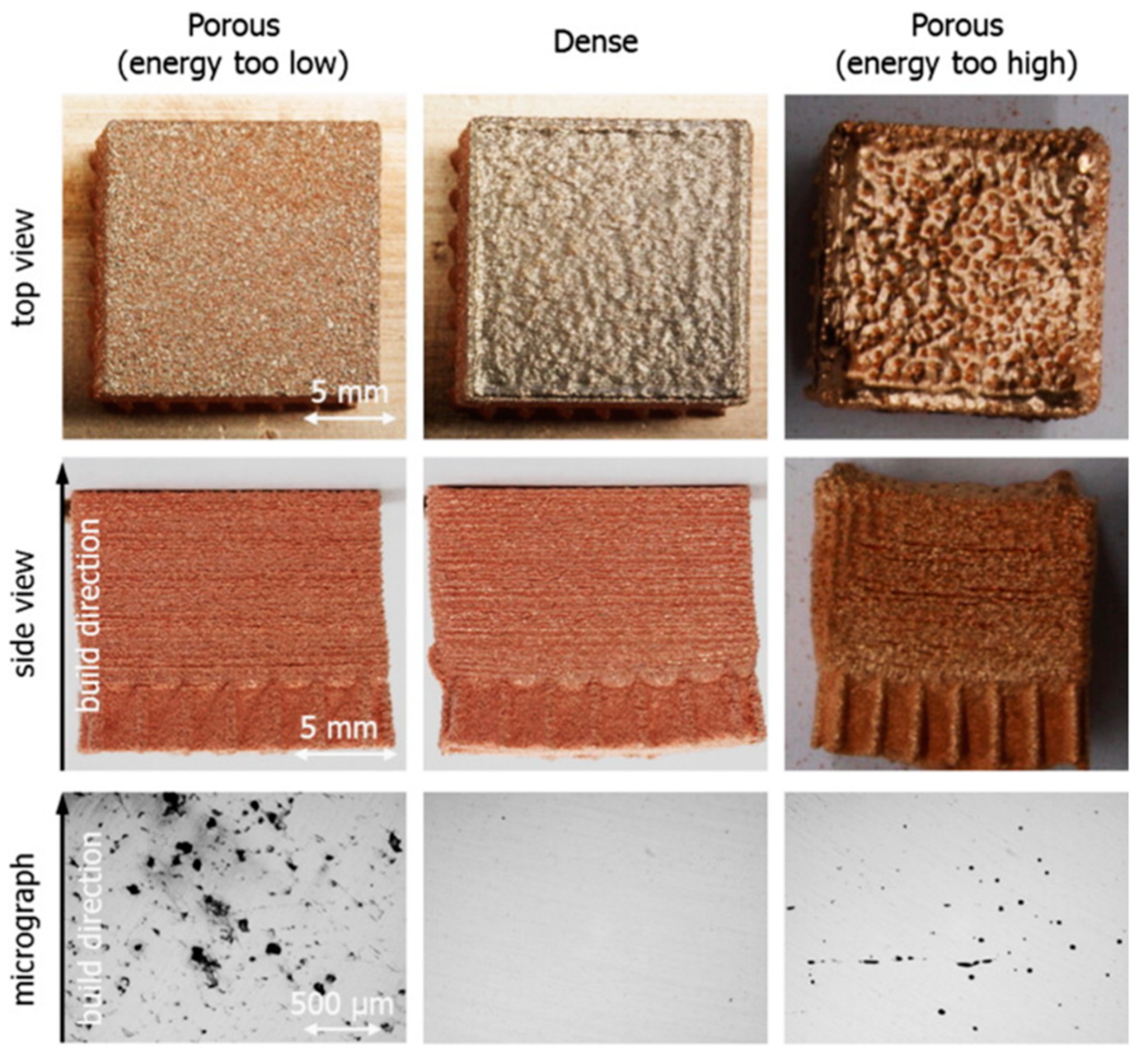
2.1. Selective Laser Melting

Selective laser melting (SLM) is a widely used powder bed-based process to fabricate metallic parts [44,45,46,47,48]. The building process starts with spreading metal powder in thin layers across a work area (Figure 1a) [1,3]. The metal powder is usually fed by a hopper while a recoater blade is used to ensure uniform powder distribution (Figure 1b, Step I). Then, a galvanometer scanner is employed to direct a high energy density laser beam across the deposited layer of the metal powder (Figure 1b, Step II). According to the CAD data of the fabricated part, only metal powder in the selected areas is exposed to the laser beam and melted along the part contour and filling in the XY plane (Figure 1a, B-B). The build platform is lowered (Figure 1b, Step III) subsequently and a new powder layer is deposited for the next laser scanning step. These three steps are repeated until the required part is fully built.
The build plate is usually connected to support structures which are necessary for the part’s fixation in the powder bed and heat dissipation (Figure 1a, Detail A). The distortion of the printed parts can be avoided by pre-heating the build plate to lower thermal gradients and reduce residual stresses during the SLM process. Inert gas such as nitrogen or argon is continuously supplied to the building chamber to provide an inert atmosphere for protecting the metal powder and the heated metal parts from oxidation. Once the printing process is completed, the substrate plate can be removed from the printed part. Important process parameters such as layer thickness, hatch spacing, laser power, and scanning speed need to be optimized to fabricate high quality printed parts [1,3].

2.1.1. Indirect Selective Laser Melting

Badrinarayan et al. [49] first reported the indirect manufacturing of pure copper parts using the SLM method. A powder mixture of copper and poly(methyl methacrylate) (PMMA) was used as a feedstock for the printing process. Since PMMA acted as an intermediate binder, it was melted during the laser scanning process to bind the copper powders and form copper green parts. The green parts were debinded under reducing conditions afterwards and the resulting copper parts were sintered for several hours. However, the mixing ratio of PMMA in the fabrication process was too high (8 wt.%), leading to the low green density (under 27%) [49,50]. Consequently, the sintered copper parts had a density much lower than the theoretical density (about 77–88%) with the introduction of significant porosity. To address the issue, polymer-coated granules of small copper particles and bimodal mixed powders could be used to improve the powder packing density. Another drawback of the indirect SLM was that the impurities from the debinding process could be introduced to the final copper parts and might lower their properties [49,50].

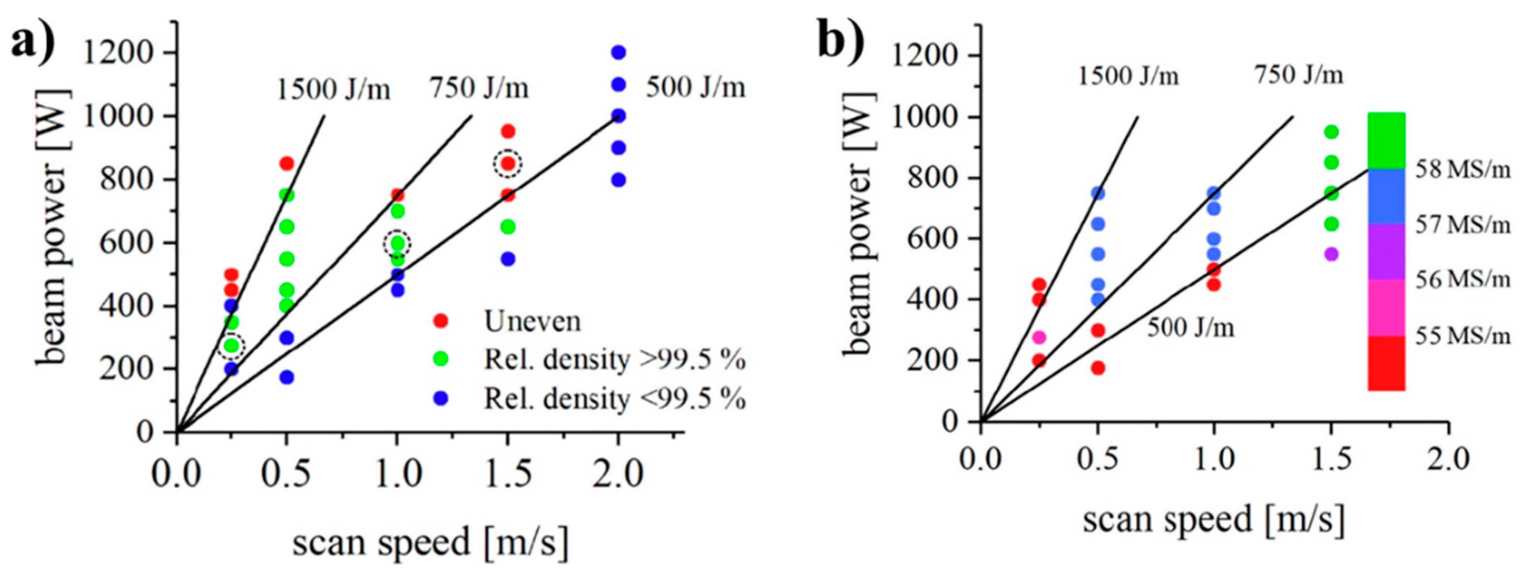
2.1.2. Direct Selective Laser Melting

Most commercial SLM systems use continuous wave and long-pulse lasers working in the near infrared radiation (IR) with a wavelength of about 1 µm [51,52]. Although SLM has been demonstrated for many materials ranging from metals to polymers and ceramics [53,54,55,56,57,58], the processing of materials with high thermal conductivities and high melting points such as pure copper is still challenging [59,60]. In addition to the rapid heat dissipation problems, reflectivity of copper to conventional laser light near IR is very high [61,62,63], resulting in low deposition of laser energy in the materials for the melting process [51]. Therefore, to achieve high laser energy density for fabricating dense copper parts, greater laser output power and lower scanning speed, layer thickness, and hatch spacing are required [52,59,64].
Generally, the minimal laser power for a successful SLM of pure copper is approximately 300 W, although some studies have reported the fabrication of copper parts at lower laser powers [65,66]. Lykov et al. [65] studied the SLM process of pure copper powder using a system equipped with a 200 W CO2 laser source. The process used a scanning speed ranging between 100 and 150 mm/s whereas the layer thickness and hatch spacing were fixed at 50 μm and 0.12 mm, respectively. Although the absorptance of pure copper powder for CO2 laser was very low (only 0.26), the copper powder could be selectively melted since the laser beam diameter was adjusted to as small as 35 μm to obtain sufficient power density for the melting process. Consequently, the printed copper parts had dense structures with good surface finish quality and no dimensional distortions were observed. Specifically, the relative density of the printed parts could be as high as 88.1% while their tensile strength could reach 149 MPa [65].
In another approach, Kaden et al. [52] reported a successful SLM process of pure copper by using ultrashort laser pulses with 500 fs pulse duration at a center wavelength of 1030 nm. At a 20 MHz repetition rate, the lasers could provide extremely high pulse energy (1–1.5 µJ) and line energy (100 J/m), which were sufficient for copper melting. The powder layer thickness and laser spot size were controlled at 30 µm and of 35 µm, respectively, to fabricate both bulky and thin-walled copper structures with thicknesses below 100 µm (Figure 2). The scanning electron microscope (SEM) images in Figure 2b suggested that the printed parts had porous structures with melting beads formed during the powder melting. This might stem from the large powder size (35 µm) compared to the laser spot diameter (35 µm) employed in the process. Therefore, the use of copper powder with small grain sizes was recommended to reduce porous structures of the printed copper parts and improve their relative density [52].
By using a laser source with much higher power, Ikeshoji et al. [64] could fabricate 3D copper parts with a relative density of up to 96.6% by SLM. In the fabrication process, the laser power was set at 800 W and the used hatch pitch was in a range of 0.025–0.12 mm. Additionally, the scanning speed and powder bed thickness were fixed at 300 mm/s and 0.05 mm, respectively. As can be seen in Figure 3a, the surfaces of all the printed cubes had rough texture and ballshaped asperities with no severe oxidation observed. These ball-shaped asperities might stem from the nonmolten residual powder particles while large asperities might be formed by splatter. Also, the surface texture suggested the presence of voids within the copper structures [64].
Due to the large asperities, smooth powder bed surfaces might not be achieved during the squeezing process. Internal voids could be formed at the shadow of the laser irradiation under the ball-like asperities and, therefore, lowered the relative density of the printed parts. As shown in Figure 3b, the relative density of the printed parts decreased at narrower hatch pitches, although the asperities could be exposed to the laser beam several times and melted down to fill the voids during the laser scanning process. Besides, transient heat transfer including melting and solidification was analyzed by the finite element method (FEM) to study the effects of hatch pitches on the SLM process of pure copper. The various predicted dimensions of the melt pool with time indicated a slight overlap for wider hatch pitches and instability for narrower hatch pitches. This result suggested that the relative density of the printed copper parts was strongly related to the hatch pitch [64].
Later, a feasibility window of the SLM process of pure Cu powder was investigated by Colopi et al. [59] using a 1kW laser source. A total of 70 experimental conditions were conducted by varying the laser power, layer thickness, and scan speed in ranges of 200–1000 W, 50–100 µm, and 1000–4000 mm/s, respectively. The process outcome was classified into three categories: not fused (insufficient solidification), delamination (insufficient interlayer bonding), and acceptable (no evident defect). As shown in Figure 4a, the process using a layer thickness of 50 µm had the widest stability region, which might stem from its higher process resolution.
The “delamination” defect occurred in both layer thicknesses, suggesting the crucial role of inter-layer bonding on obtaining a stable powder bed densification. The occurrence of this defect at low laser power indicated the instability of the process melt pool (Figure 4a). Since the previously deposited copper layer had high thermal conductivity, thermal cooling could be elevated while melt pool stability might be hindered. Besides, the formation of the inter-layer defect might lead to thermally insulating gases in between the layers and, hence, limit the penetration of the melt pool to the previous interlayer defect. Consequently, the delamination issue might be further worsened due to the formation of thermally-induced stresses, resulting in more defect formation and part deformations [59].
As shown in Figure 4b,c, the relative density of the printed copper parts yielded up to 97.8% of the separate measurement between the core volume of sections and the border. The porosity in the border regions was always higher, which might be attributed to the temperature differences between the border and the central region. Due to thermal accumulation, most internal regions could reach higher temperatures compared to the border. Furthermore, the border was usually in contact with cooler powder in the powder bed during the scanning process. Since copper has very high thermal conductivity, strong thermal dissipation could be achieved in the border areas, resulting in their partial melting and higher porosity. The process parameters optimized the feasibility window which could be used to produce complex 3D copper parts, as shown in Figure 4c [59].
Jadhav et al. [51] studied the influences of different laser scan parameters on the textural development of SLM-printed copper parts. The fabrication process used a 1 kW laser source, with a beam diameter of 40 μm, and a layer thickness of 30 μm. At optimum processing conditions, printed parts with a relative density of more than 98%, electrical conductivity of 88% IACS (International Annealed Copper Standard definition of 58 MS/m as 100% IACS for electrical conductivity), and thermal conductivity of up to 336 W/m.K could be produced (Figure 5a,b).
The analysis of the crystallographic texture of the SLM copper parts suggested that the crystal orientation of the YZ and middle (XY-MID) plane was relatively random. This result could be attributed to the alteration in the heat gradient directions and subsequent re-melting which were formed by applying a 90° scan rotation strategy in between the subsequent layers. However, the top surface (XY-TOP) had strong crystallographic texture owing to the solidification morphology controlled by the temperature gradients within the melt pools. Due to the extremely high laser energy density and laser power used in the process, damages of the optical coating could be formed on the laser mirror, as shown in Figure 5d [51].

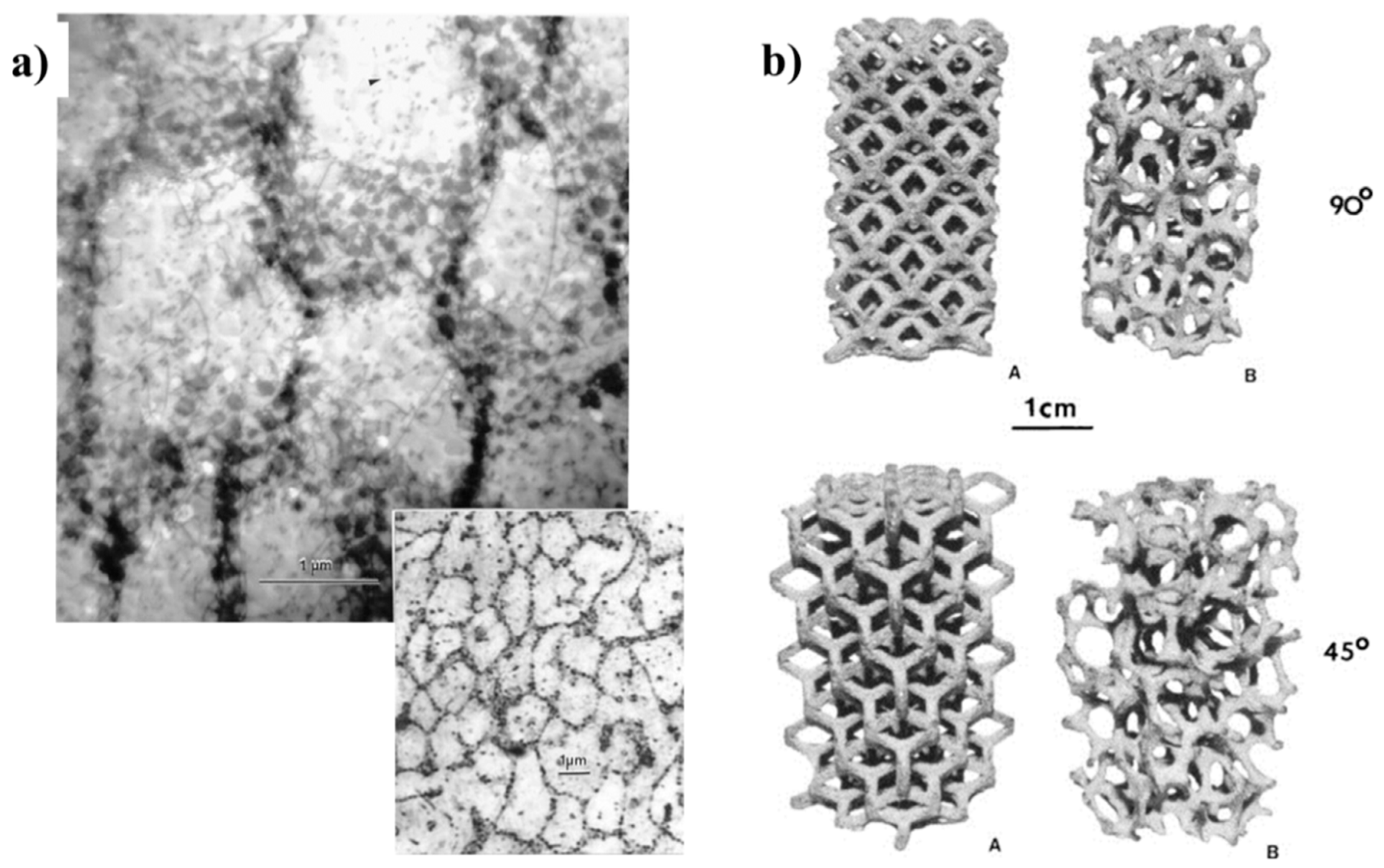
2.2. Electron Beam Melting
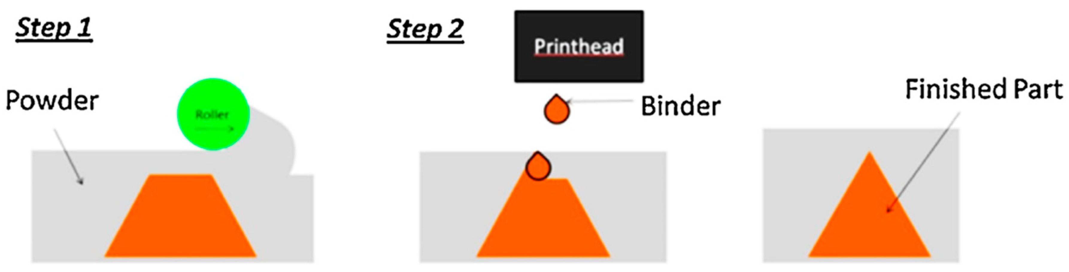
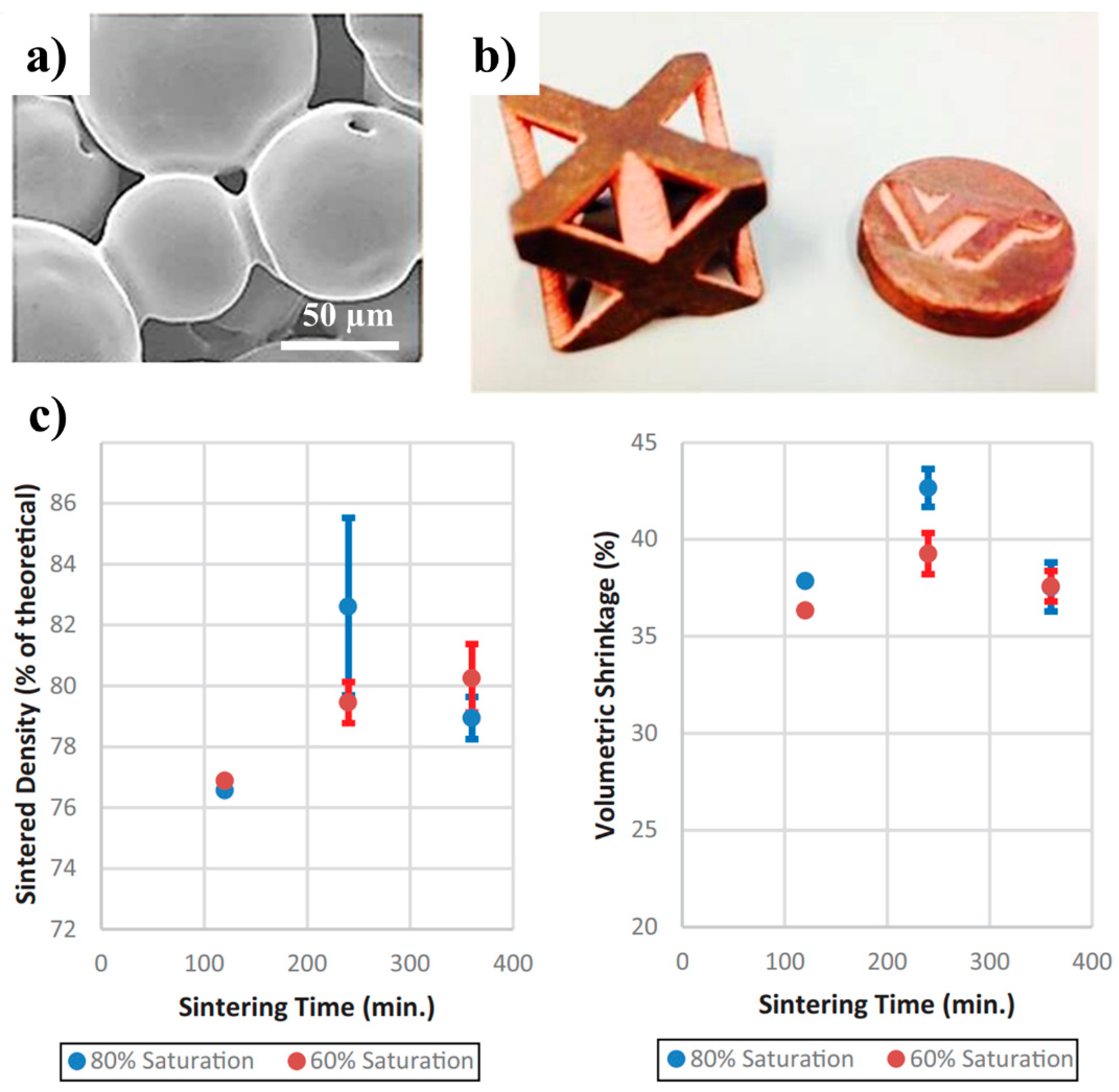
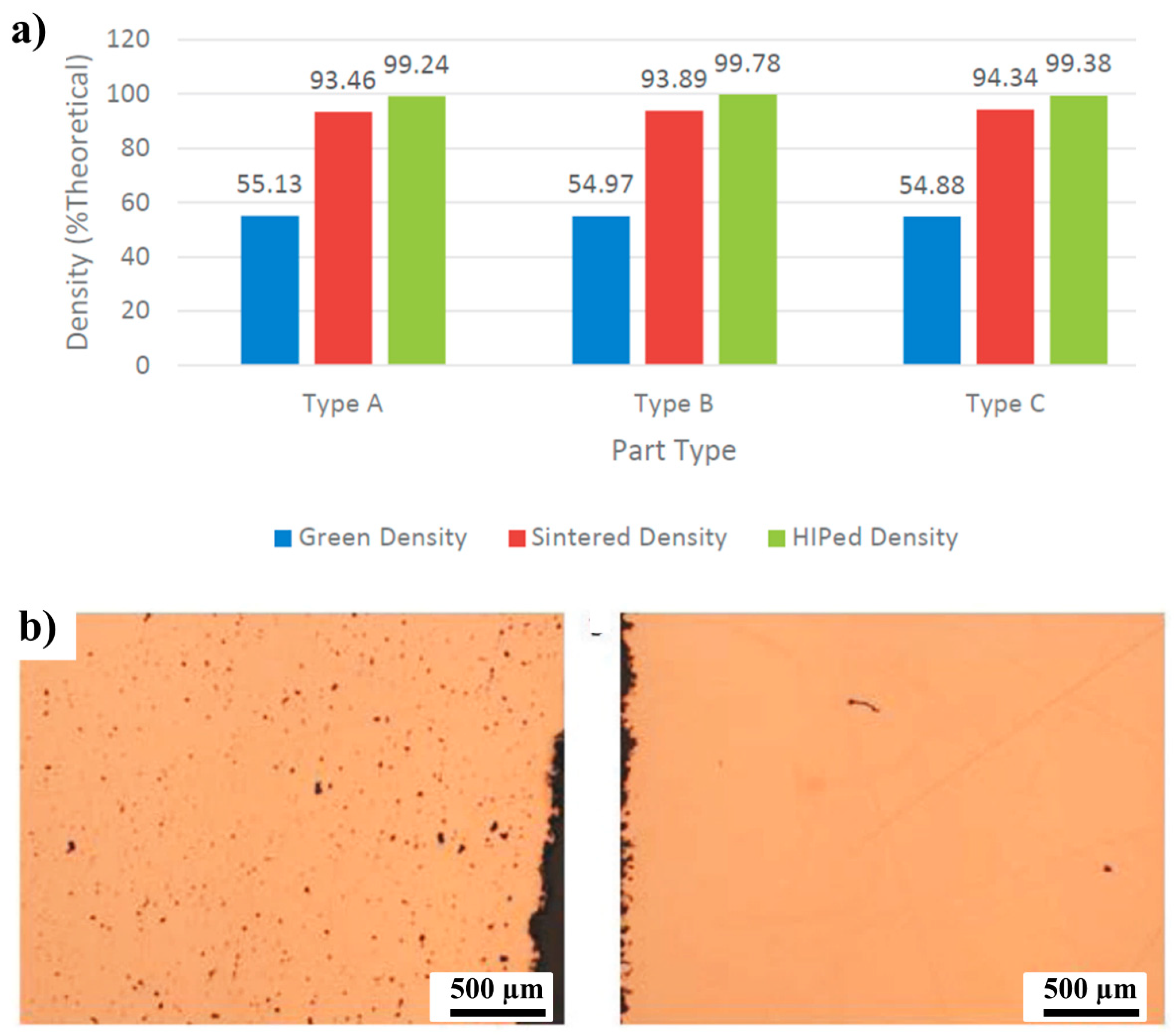
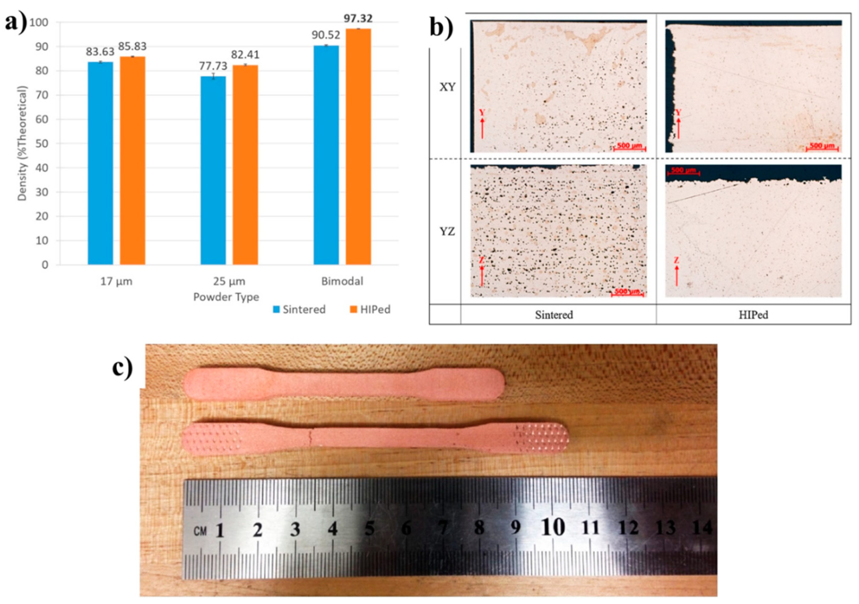
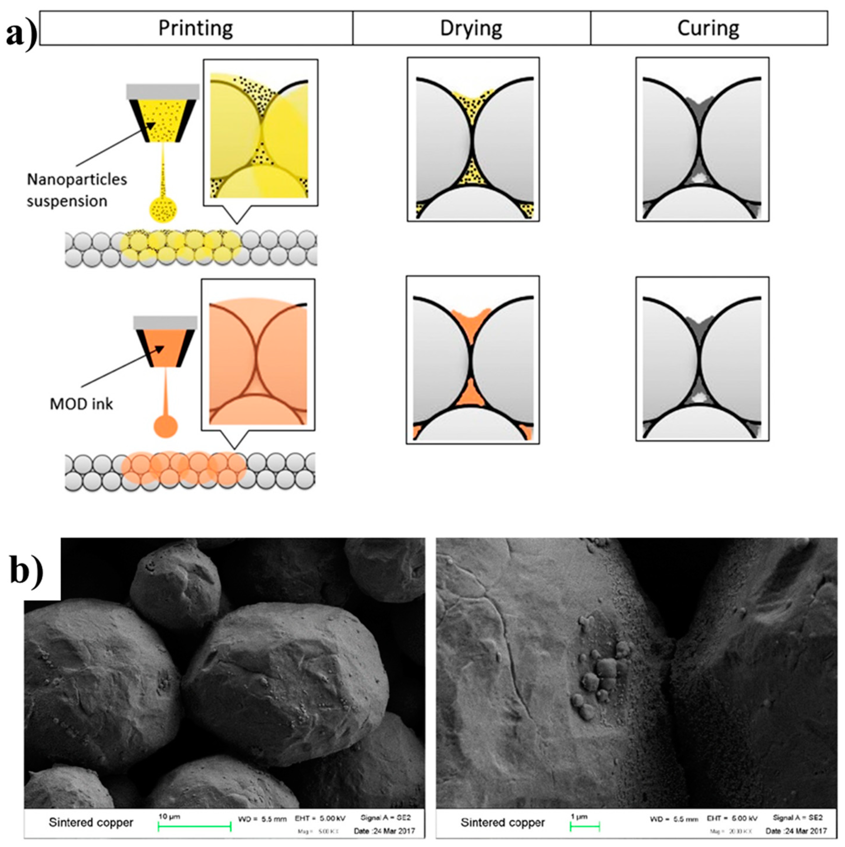
Similar to SLM, electron beam melting (EBM) is also a common powder bed-based process used to fabricate highly-dense metallic parts [67,68]. In the EBM process, metal powder from a hopper is supplied and spread uniformly on a build plate by a rake (Figure 6) [1,69]. The powder layer thickness is usually in the range of 50–200 µm. According to the CAD data, the powder is melted selectively using an electron beam as a heat source. The electron beam is produced by an electron gun and accelerated with a high acceleration voltage. Then, electromagnetic lenses are used to focus the beam and a magnetic scan coil is employed to direct it to selected areas of the metal layers in the XY plane. Important EBM process parameters such as electron beam power, scan speed, and focus of the electron beam usually depend on the speed function, beam current, and focus offset, respectively [70].
At first, a defocused beam pre-heats the powder bed by scanning the powder bed surface several times. Then, a high beam current and proper scan speed are employed to heat and sinter the powder. Similar to the SLM process, the build plate in EBM is then lowered and metal powder is fed and spread uniformly across the work area. The process of powder deposition, powder pre-heating, electron beam scanning, and build plate lowering is repeated until the part printing is completed. The EBM process operates under a vacuum and helium is fed to the work area to prevent the metal powder from electrical charging while improving the heat conduction and cooling of the melt [1,71].
Since electrons have different absorption and reflection mechanisms compared to photons, the EBM method is not affected by the optical reflectivity of materials and most of the energy in EBM is deposited within the materials [1,4,40,72]. Therefore, this method has a high potential for the processing of pure copper [73,74]. Furthermore, the sintering step of copper during the EBM process can be extremely short due to its high electrical conductivity. In fact, the copper powder might not be removed if preheating is too high or too long because it has high sintering activity [1,4,40]. Yang et al. [28] reported the fabrication of pure copper with orthotropic re-entrant auxetic structures using EBM. Because of the high thermal conductivity of copper, the dissipation of thermal energy during the melting process was severe, resulting in large variations in the dimensions and mechanical performance of the printed copper parts. Therefore, more process optimization was required to improve the surface quality and accuracy of the printed parts.
Since copper is quite sensitive to oxidation, its storage and handling should be considered properly [75]. Ramirez et al. [76] investigated the effects of Cu2O on the microstructure of the EBM-printed copper components with the use of a relatively impure Cu precursor powder (98.5%). The study results showed the formation of precipitation–dislocation architectures because of directional solidification during EBM (Figure 7a). Interestingly, these precipitation–dislocation architectures improved the hardness of the parts from HV 57 for a base-plate to HV 88 for EBM-printed products. Similar phenomenon was also observed in their later study of the open-cellular copper structures (Figure 7b) produced by EBM of higher purity copper powder (99.8%) [26].
A comprehensive performance of pure copper parts fabricated by EBM using three different copper powder configurations was reported by Frigola et al. [40]. The printed copper parts exhibited good properties with a relative density of 98.6%, electrical conductivity of 97% IACS, thermal conductivity of 390 W/mK, and yield strength of 76 MPa. More interestingly, the copper cathode fabricated by the EBM process showed good performance during high power radio frequency (RF) testing, which was comparable to other cathodes conventionally machined from wrought oxygen free copper material.
Later, a much higher relative density (up to 99.95%) of EBM-printed copper parts was achieved by Lodes et al. [77]. The results in Figure 8 show that the samples fabricated at higher line energies were denser for all beam velocities. Part density was lower at the very low line energy input because the powder could not be melted completely, resulting in layer defects and porous printed parts. However, the use of too great an energy input could lead to local overheating and swelling of the sample. Additionally, overheated copper powder could stick to the melt surface during raking, resulting in binding defects and porous areas. At optimum line energy, the built sample was almost fully dense with no binding defects observed.
Raab et al. [78] fabricated 3D copper parts with high relative densities (up to 99.95%) and good physical performance using EBM. At volume energies higher than 60 J/mm3, an electrical conductivity of up to 55.82 MS/m (96.24% IACS) and thermal conductivity of 400.1 W/mK could be achieved. The study results also suggested that pores and impurities such as oxides or carbides inside the printed copper parts might lower their electrical and thermal performance due to the reduced conduction cross-section. Later, Guschlbauer et al. [79] reported the fabrication of EBM-printed copper parts with excellent physical properties at different process parameters, as shown in Figure 9. At optimum conditions, the printed parts could obtain a relative density greater than 99.5%, an electrical conductivity of more than 58 MS/m (>100 IACS), a thermal conductivity of more than 411 W/mK, and tensile strength of 177 MPa. The uniform distribution of oxides in the copper matrix of the printed parts and no elevated oxygen content observed at the grain boundaries suggested that oxygen might have no significant role in crack formation during the tensile test. Instead, cracks might be generated by internal stresses formed during the manufacturing process [79].

2.3. Binder Jetting

Binder jetting (BJ) is a 3D printing process in which one or two inkjet printheads are used to selectively deposit a liquid binding agent on the top of a powder bed to join powder materials [21,80,81]. The schematic of BJ process is shown in Figure 10 [21]. In Step 1, a roller is employed to spread metal powder uniformly across the platform to form a thin layer. Then, an inkjet printhead moves along the X- and Y-directions to selectively distribute binder droplets into the powder layer. The binder bonds the powder particles to produce a printed cross-sectional layer. Then, the build platform lowers (Z direction) for a small distance, the roller spreads a new powder layer, and the binder injection process repeats.
When all the layers are deposited, the final glued part, usually called the ‘‘green part’’, is formed. Then, the binder is cured at elevated temperature to improve the green part strength for easy handling. The printed part experiences further sintering to achieve its final strength and density. During the sintering process, the binder is removed and the loosely packed powder is bonded together through powder sintering and densification. In the BJ process, many processing and post-process sintering parameters such as the binder saturation, spreader speed, layer thickness, and sintering profile affect the final density and properties of the printed parts [82,83,84,85,86,87]. Compared to SLM and EBM, BJ has several unique characteristics for fabricating complex pure copper parts: (i) no requirements of support structures, expensive energy sources, and enclosed chamber; (ii) scalable technology; (iii) no concerns over a material’s reactivity, melting point, thermal conductivity, and optical reflectivity; (iv) leveraged understanding of well-studied powder metallurgy processes due to the separation of part creation and powder sintering steps [21].
Bai et al. [21] first studied the 3D printing of pure copper via BJ of copper powders with median diameter of 75.2 µm, 15.3 µm, and 16.5 µm. Large powder size is usually preferred in the BJ process for powder spreading while small powder is crucial for sinterability, surface quality, and resolution. PM-B-SR2-05, a thermosetting polymer, was used as a binding agent in the process due to its minimal ash residue after debinding. The crucial printing parameters in the green part production were binder saturation ratio and layer thickness. The binder saturation ratio (the percentage of air space between the powder particles occupied by the binder volume) needs to be sufficient for the fabrication of a strong green part.
After sintering, green parts with a maximum relative density of 85.5% were achieved. The shrinkage and sintered density were found to be proportional to the temperature in a range of 1060–1090 °C. A purity of 97.3% and improvement of 25.3% in the sintered density could be achieved by sintering the printed parts in a reduced atmosphere, as shown in Figure 11. The printed sintered copper parts could only have a tensile strength of 116.7 MPa due to their high porosity. One main challenge of the BJ process is to improve the densification and part sinterability while satisfying the size requirements of the copper powder [21].
In a later study, Bai et al. [80] reported the benefits of using bimodal powder mixtures in the BJ of copper parts. In the process, five powder mixtures formed from copper powder with different diameters were employed as the process feedstock. The study results showed that the bimodal powder mixtures could improve the powder packing density by 8.2% and powder flowability by 10.5%, compared to the monosized powder counterparts. More importantly, the printed green part and the sintered density could increase by up to 9.4% and 12.3%, respectively, while a decrease of 6.4% in sintering shrinkage was observed due to the use of the bimodal powder mixtures. Another benefit was that less energy input might be required for the process using the bimodal powder mixtures as it was less sensitive to the sintering conditions.
Since coarse powder and loosely packed powder beds are used in the BJ process, the final printed copper parts usually contain high porosity with low mechanical properties. One effective approach to address this issue is to apply post-process heat treatments, such as hot isostatic pressing (HIP) [88,89]. Kumar et al. [36] applied HIP to the final printed copper parts with three different dimensions (Type A: 16 mm × 16 mm × 4 mm type B: 32 mm × 8 mm × 4 mm, and type C: 16 mm × 8 mm × 4 mm). As seen in Figure 12a, the relative density of the sintered parts could reach 99.47% after HIP treatment. This result was supported by a significant decrease in pores observed in the sectioned parts shown in Figure 12b, suggesting that HIP could densify the printed copper parts to nearly full density.
In a later study, Kumar et al. [90] investigated the combined effects of bimodal powder mixtures and HIP treatment on the BJ printed copper parts. In the process, the copper parts were printed from three powder configurations: two with 17 and 25 μm powders and one with a bimodal powder mixture of 5 and 30 μm powders. The improvement in density shown in Figure 13a indicated that the printed parts with bimodal configuration had the best densification effects with a relative density of 97.32% after HIP. The results also suggested that HIP was only an effective post-treatment when the sintered BJ parts had a minimum relative density of 90%, which could be achieved by using bimodal powder mixtures. The relative density of 99.47% in their previously study [36] could not be replicated due to the problems with clogged inkjet nozzles and differences in the powder quality. More importantly, due to the reduction in porosity after HIP application, both tensile strength and ductility of the bimodal samples increased from 144.9 to 176.35 MPa and from 18.81% to 31.28%, respectively.
The effects of binders on the BJ process of pure copper were studied by Bai et al. [91] using two different nanoparticle binder systems: colloidal organic binder (a conventional polymer binder with suspended copper nanoparticles) and inorganic nanosuspension (an inorganic copper nanosuspension ink). They found that the jetted nanoparticles could produce denser green parts. However, there were no significant differences in the sintered density compared to copper parts printed by conventional organic binder. This might stem from the offset of the reduced sintering densification to the density obtained in the green part. However, the inkjetted nanoparticles could reduce the grain size of the sintered parts by hindering the grain growth during the sintering process, leading to their improved tensile strength. Moreover, the use of these metal binders could enhance the metal purity and structural integrity of the sintered parts. Besides, a higher weight percentage of copper nanoparticles in the printed copper parts could be achieved at higher binder saturation ratios, resulting in better green part strength as well as higher green part and sintered part density.
In another study, Bai et al. [92] used metal-organic-decomposition (MOD) ink as a binder in the BJ process of copper. As the MOD ink is particle-free [93,94] it can avoid the common issues found in the BJ process using particle suspensions such as particle oxidation, sedimentation, and nozzle clog problems. To validate this concept, copper organometallic complex with a metal content of 7.4 wt.% was synthesized for BJ printing of pure copper (Figure 14a). During the fabrication process, an overhead heater was used to dry the MOD ink between layers by removing the solvent. Then, copper nanoparticles were precipitated and sintered from organometallic complex to bond the copper powder when the printed parts were cured in a reducing atmosphere (Figure 14b). However, the green parts using MOD ink were weaker than those printed with the conventional polymeric binder. Although the sintered copper parts printed by MOD ink had a denser core section, their outer shell was more porous. This porous shell may stem from the powder loss due to weak powder bonding. Consequently, the relative density of the copper parts printed by MOD ink was lower than that of the conventional binder counterparts.

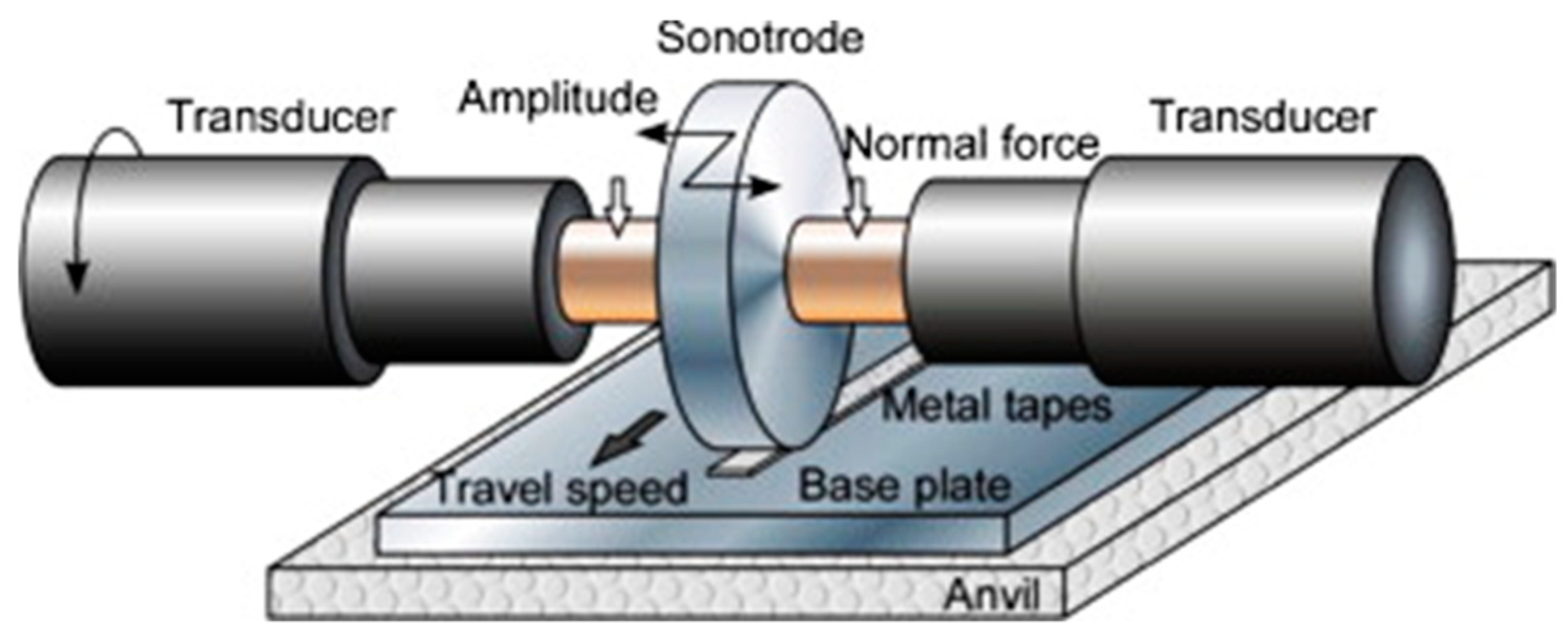
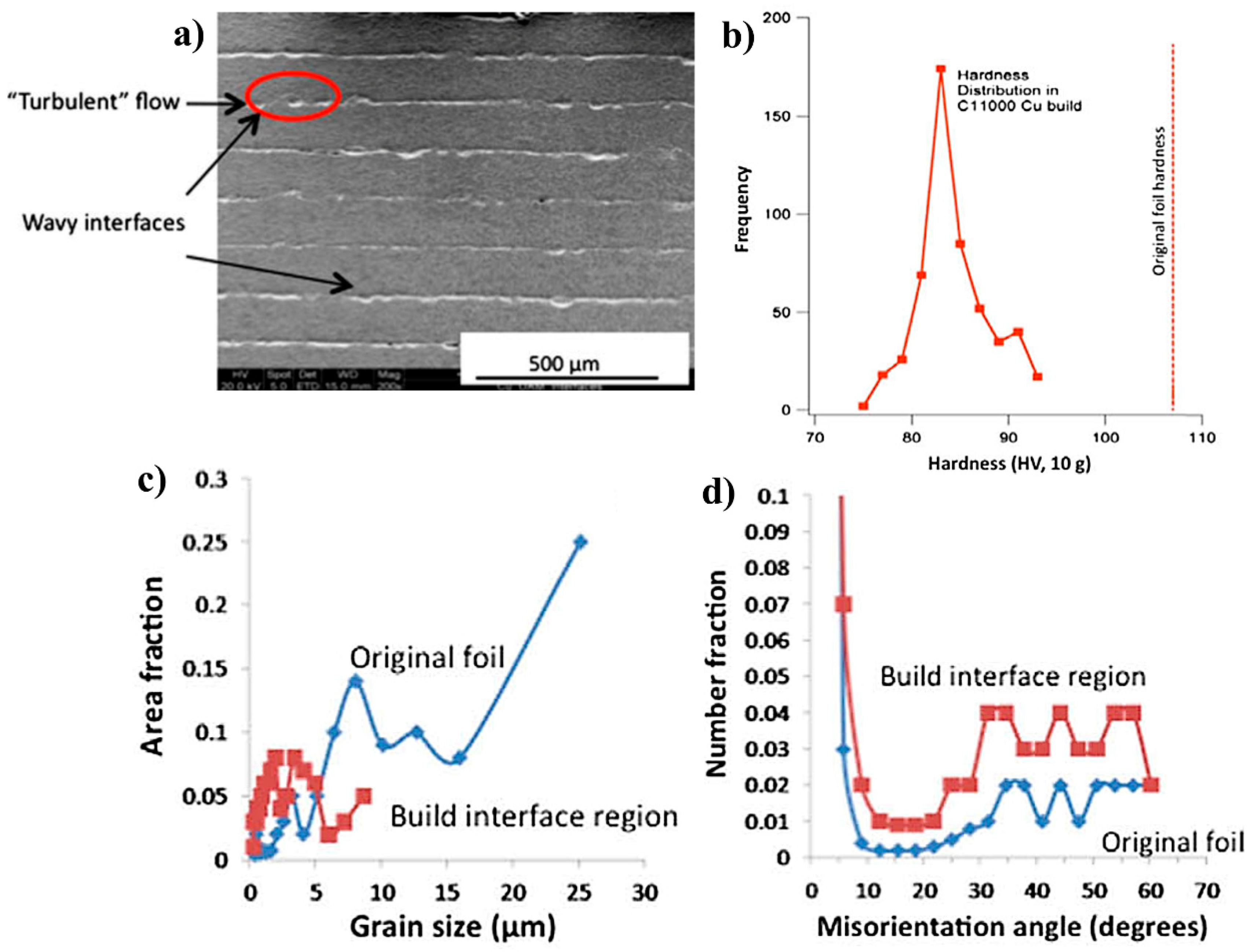
2.4. Ultrasonic Additive Manufacturing (UAM)

Ultrasonic additive manufacturing (UAM) is a manufacturing method using thin metallic foils or tapes as feedstock to fabricate 3D parts [95,96,97,98]. In this method, an ultrasonic wave and mechanical pressure are applied on metallic tapes at room temperature to bond the interfaces of the stacked tapes by diffusion [99]. 3D parts can be built by bonding the stacked tapes layer-by-layer without the use of any heat source. The metallic tapes are usually cut into designed shapes before ultrasonic consolidation bonding. To achieve good finishing, polishing is usually applied during or after the consolidation process. Figure 15 illustrates the working process of an UAM equipment [95].
The building process starts with the laying out and stacking of a metallic tape on a base plate. Then, a sonotrode applies ultrasonic vibrations laterally to the tape when it rolls along the tape length [99]. This bonds the metallic tape to the previously built parts to form a seam weld. During this process, the rapid “scrubbing action” between the faying surfaces generates the bonding. Typically, the first tape is welded onto the base plate, followed by the bonding of the next tape. After all the layers are built, the final part is cut from the base plate and polished for desired surface finishing. Therefore, the UAM process can produce metallic parts of complex shapes and designs. During the bonding process, frictional heat at the bonded interfaces is produced, leading to the increased temperature of the consolidated region. Therefore, a short cooling period between the manufacturing of each layer is required to avoid thermal residual stress [95].
Welding copper tapes are usually difficult due to material hardening and oxidation issues, leading to the requirement of high power used in the process (up to 9 kW) [95,96,100]. Sriraman et al. [96] studied the bonding characteristics formed during a very high-power UAM of copper tapes. In the study, C11000 copper tapes (170 mm × 25 mm × 0.15 mm) were successively bonded via ultrasonic seam welding at room temperature. The welding process was conducted at an amplitude of 36 µm, static force of 6.7 kN, and travel speed of 30 mm/s. The final built part was comprised of 13 layers to reach a height of about 2 mm. Figure 16a shows the interfaces of the built sample with wavy features. It might stem from the violent plastic flow of the material which was formed along the ridges and valleys between the contacting layers during the scrubbing process. Hardness distribution shown in Figure 16b suggests that the material might be uniformly softened and the hardness values throughout the built part were about 11–23% lower than those of the as-received foils [96].
As seen in Figure 16c, the grain size of the copper foils at the foil interface reduced from 25 to 10 µm after the processing [96]. Moreover, a larger fraction of grains with high-angle misorientations were observed in the built part (Figure 16d). The findings indicated that there was recrystallization followed by the movement of grain boundaries across the interfaces, resulting in metallurgical bonding between the layers. Additionally, the initial coarse grain structure might experience plastic deformation and recovery during the welding process. Their later study on the thermal transients during the process suggested a strong correlation between the interfacial temperature and plastic deformation heating [95]. Moreover, vibration amplitude had strongest effects on interfacial temperatures as dynamic plastic shear strains at the asperities were higher with increasing amplitudes. Although the UAM process could produce fully dense parts, void defects might be formed within the material’s internal structure during the fabrication process, lowering its electrical and mechanical performance.

3. Advantages and Challenges of 3D Printing Methods of Pure Copper

Table 1 compares the characteristics of all 3D printing methods of pure copper. In both direct SLM and EBM, high energy power is required to heat the copper powder to its melting point for part fabrication. However, the required energy of direct SLM is much higher than that of EBM due to the low energy absorption of pure copper with conventional lasers (wavelength of 1 µm) [41,59,101,102,103]. Moreover, the high reflected laser radiation in direct SLM of pure copper can damage the system’s components. These issues can be addressed by (i) improving the optical absorption of copper by using a green laser with a shorter wavelength (515 nm) or chemically modifying the surface of the copper powder and melt; and (ii) applying advanced multi-variate ray tracings to eliminate the back focal points on the locations of the laser mirrors [51]. The required energy in the EBM of copper is lower than that in direct SLM because optical reflectivity of the materials do not affect the EBM process [4,40]. However, the EBM beam size is larger than the laser spot size in direct SLM, limiting the fine features size of the EBM-printed parts. Due to rapid melting/solidification of copper powder, the copper parts fabricated by both SLM and EBM have many issues in the full melting process, such as thermal residual stresses and thermally-induced deformation [2,27]. These issues can be minimized by properly designed anchors or support structures which dissipate heat and prevent part deformation [1,41].
The printing temperatures in the indirect SLM, BJ and UAM processes are much lower than those in direct SLM and EBM (lower than 50% of copper’s melting temperature) [21,27,49,50,95,96]. This prevents many issues formed in full melting processes, such as thermally-induced deformation and thermal residual stresses. Both indirect SLM and BJ need quite low power to fabricate green parts, but post-processing such as green part curing, debinding, and sintering is required to achieve the final metal parts [21,36,49,50]. The final sintered parts usually have low density and high porosity, which require further post-processing such as HIP to obtain fully dense parts [36,90]. Residual impurities from the debinding process in indirect SLM are usually high, and this could affect the performance of the final printed parts [49,50]. The UAM can produce fully dense parts without post-processing. However, this process requires high power to process pure copper due to material hardening and oxidation issues [27,95,96].
Table 2 compares the relative density, electrical, mechanical and thermal properties of the printed copper parts fabricated by different methods. Performance of the parts fabricated by UAM is not presented because no data are available in the literature. As can be seen, EBM can fabricate copper parts with the best value of relative density (99.95%), electrical conductivity (102% IACS), tensile strength (177 MPa), and thermal conductivity (411.89 W/mK). In contrast, copper parts from indirect SLM have the poorest performance with a relative density of 84.8% and strength of only 8 MPa. Interestingly, parts printed by JB have a high relative density and strength of 99.7% and 176.35 MPa, respectively, but no data for electrical and thermal conductivity are available. For direct SLM, the printed parts have a high relative density (99.6%) and good physical performance with an electrical conductivity of 88% IACS, tensile strength of 149 MPa, and thermal conductivity of 336 W/mK.

4. Applications and Opportunities

4.1. Complex Heat Exchanger

One of the common applications for 3D printing of pure copper is complex heat exchangers [12,13,104,105,106]. Heat transfer components such as micro reactors, radiators, exchangers, or coolers could have improved function and efficiency by additive manufacturing approaches. An effective heat transfer in a liquid cooling system usually has a reliable and complex structure with high surface-volume ratio so that the flowing liquid can have many contacts with the surface area of the components. Moreover, their structure needs to be reliable to provide high pressure and resistance against fluid crossing between channels or fluid leakage. Notably, heat exchangers fabricated by conventional processes such as soldering or diffusion bonding are costly and insufficiently reliable because of their complex assembly [12,13]. Due to the single-step process of 3D printing, the printed components have no joints and, therefore, lower the risk of leakage [12,13]. Moreover, higher efficiency of the heat transfer can be achieved by maximizing the surface–volume ratio because many complex internal structures or intricate channels in confined space can be designed and fabricated by 3D printing, as shown in Figure 17a [13].
Furthermore, many materials with high thermal conductivity such as copper or copper alloys can be used for 3D printing of heat exchangers. Figure 17b presents an example of a compact cooler unit fabricated by SLM. The component (46 mm × 59 mm × 15 mm) has many cooling fins with a thickness of 0.3 mm to ensure efficient heat exchange. A high surface–volume ratio and turbulent flow of the coolant are achieved by optimizing the ribbing within the component [13]. In another approach, open-cellular copper structures with densities ranging from 0.73 to 6.67 g/cm3 have been fabricated by EBM, as shown in Figure 17c [26]. The printed structures had hardness values of more than 75% of commercial Cu parts, exhibiting great potential for complex, multi-functional electrical and thermal management systems and heat exchange devices.

4.2. Induction Heat Coil

Generally, induction heat coils have various shapes and sizes which are often highly customized for different applications [27]. Moreover, they usually have complex structures with curved paths or helical shapes and hollow feature for water cooling. Therefore, the production process of induction coils is usually tedious and time-consuming because they are usually fabricated manually with customized design. These features make induction coils a good candidate for 3D printing due to its advantages of fabricating complex and highly customized parts with little lead time. Induction coils are usually made of highly pure copper because the coil materials must have high efficiency fpr conducting electricity. Martin et al. [27] suggested that direct SLM, EBM and UAM are suitable for fabricating induction coils with higher precision compared to typical hand-made coils.

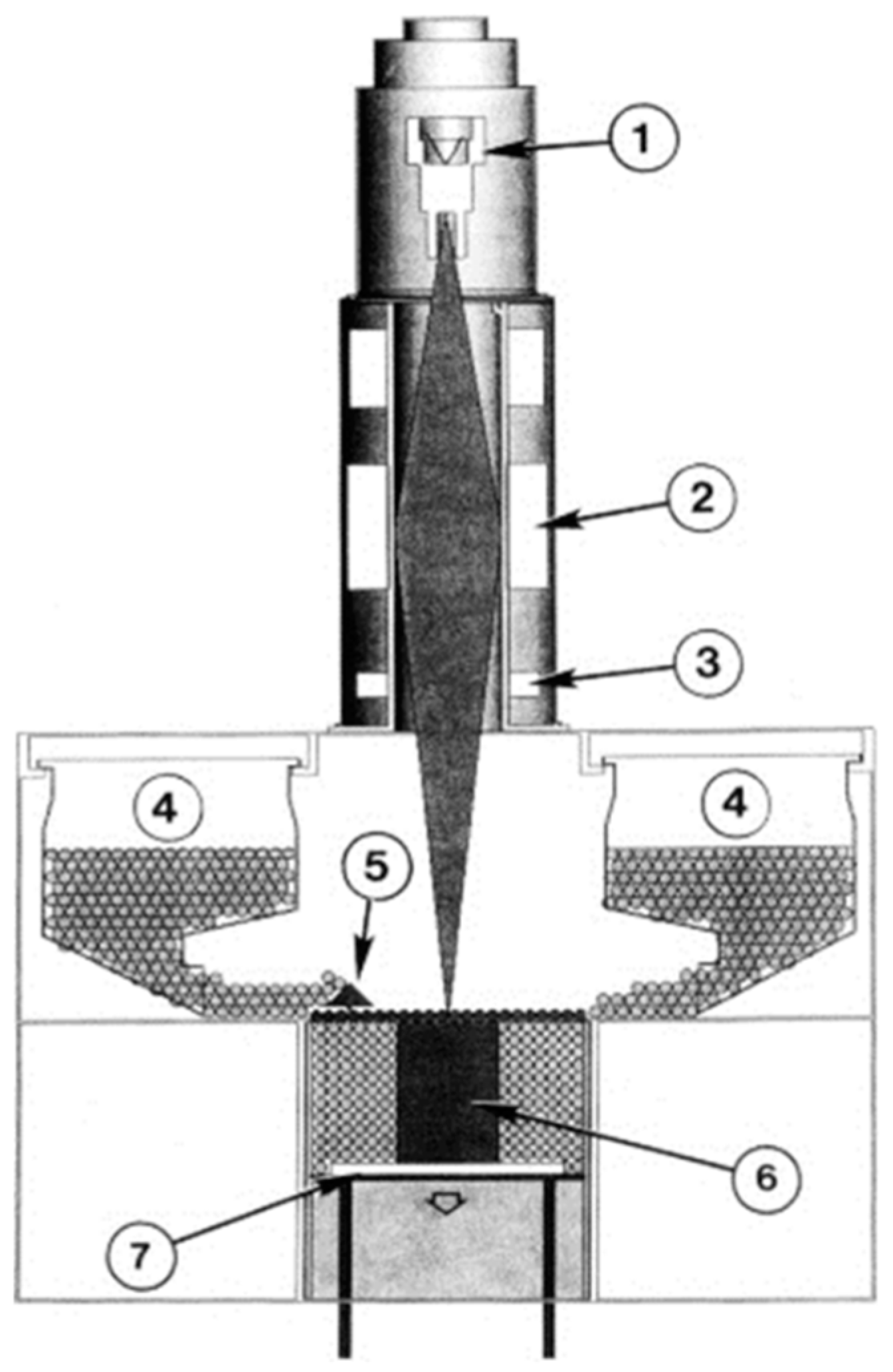
4.3. Radio Frequency Cathode

3D printing can be used to fabricate photoinjector cathodes with high RF performance. Frigola et al. [40,107] tested RF performance of the EBM printed copper cathode in a Pegasus 1.6 cell photoinjector. No other heat treatment was performed on the printed cathode before the final machining. The study results showed that during high power RF testing, the EBM printed copper cathodes had similar performance to wrought oxygen-free (OFE) copper cathodes fabricated by conventional methods. During two hours of RF conditioning, a peak electric field of 70 MV/m, a photoelectron beam with a charge of 60 pC, energy of 3.3 MeV, and quantum efficiency of ~2 × 10⁻⁵ were achieved with stable operation.

5. Conclusions and Future Direction

This paper presents a comprehensive review of research on the 3D printing methods for fabricating highly pure copper, including SLM, EBM, BJ and UAM. The advantages, challenges, and performance of the copper parts fabricated by each method have been identified and compared. Additionally, potential applications of the 3D printed copper parts in thermal management systems, heat exchange devices, RF cathodes, and induction heat coils have been demonstrated.
In the near future, the 3D printing of pure copper will most likely grow further to address all the current issues of the printing methods while exploring more potential applications of the printed copper parts. For example, the TruPrint Laser Metal Fusion (LMF) 3D printer equipped with green laser source has been developed to overcome the low absorption of pure copper to conventional laser sources and component damages [108]. Heraeus, a German technology group, has addressed the technical issues and optimized the process of 3D printing highly-conductive copper components, which opens up new industrial fields of application such as in mobility, electronics, robotics, hydraulics, medicine and aerospace [109].

Funding

This research was funded by Lloyd’s Register Foundation, grant number R-265-000-553-597.

Conflicts of Interest

The authors declare no conflict of interest.

References

  1. Herzog, D.; Seyda, V.; Wycisk, E.; Emmelmann, C. Additive manufacturing of metals. Acta Mater. 2016, 117, 371–392. [Google Scholar] [CrossRef]
  2. Zhang, Y.; Wu, L.; Guo, X.; Kane, S.; Deng, Y.; Jung, Y.-G.; Lee, J.-H.; Zhang, J. Additive Manufacturing of Metallic Materials: A Review. J. Mater. Eng. Perform. 2018, 27, 1–13. [Google Scholar] [CrossRef]
  3. Yap, C.Y.; Chua, C.K.; Dong, Z.L.; Liu, Z.H.; Zhang, D.Q.; Loh, L.E.; Sing, S.L. Review of selective laser melting: Materials and applications. Appl. Phys. Rev. 2015, 2, 041101. [Google Scholar] [CrossRef]
  4. Körner, C. Additive manufacturing of metallic components by selective electron beam melting—A review. Int. Mater. Rev. 2016, 61, 361–377. [Google Scholar] [CrossRef]
  5. Rahman, Z.; Barakh Ali, S.F.; Ozkan, T.; Charoo, N.A.; Reddy, I.K.; Khan, M.A. Additive Manufacturing with 3D Printing: Progress from Bench to Bedside. AAPS J. 2018, 20, s12018–s12248. [Google Scholar] [CrossRef] [PubMed]
  6. Dilberoglu, U.M.; Gharehpapagh, B.; Yaman, U.; Dolen, M. The Role of Additive Manufacturing in the Era of Industry 4.0. Procedia Manuf. 2017, 11, 545–554. [Google Scholar] [CrossRef]
  7. Zhakeyev, A.; Wang, P.; Zhang, L.; Shu, W.; Wang, H.; Xuan, J. Additive Manufacturing: Unlocking the Evolution of Energy Materials. Adv. Sci. 2017, 4. [Google Scholar] [CrossRef] [PubMed]
  8. Ngo, T.D.; Kashani, A.; Imbalzano, G.; Nguyen, K.T.Q.; Hui, D. Additive manufacturing (3D printing): A review of materials, methods, applications and challenges. Compos. Part B Eng. 2018, 143, 172–196. [Google Scholar] [CrossRef]
  9. Ryan, M.J.; Eyers, D.R.; Potter, A.T.; Purvis, L.; Gosling, J. 3D printing the future: Scenarios for supply chains reviewed. Int. J. Phys. Distrib. Logist. Manag. 2017, 47, 992–1014. [Google Scholar] [CrossRef]
  10. Frazier, W.E. Metal additive manufacturing: A review. J. Mater. Eng. Perform. 2014, 23, 1917–1928. [Google Scholar] [CrossRef]
  11. Guo, N.; Leu, M.C. Additive manufacturing: Technology, applications and research needs. Front. Mech. Eng. 2013, 8, 215–243. [Google Scholar] [CrossRef]
  12. Singer, F.; Deisenroth, D.C.; Hymas, D.M.; Ohadi, M.M. Additively manufactured copper components and composite structures for thermal management applications. In Proceedings of the 2017 16th IEEE Intersociety Conference on Thermal and Thermomechanical Phenomena in Electronic Systems (ITherm), Orlando, FA, USA, 30 May–2 June 2017; pp. 174–183. [Google Scholar]
  13. Neugebauer, R.; Müller, B.; Gebauer, M.; Töppel, T. Additive manufacturing boosts efficiency of heat transfer components. Assem. Autom. 2011, 31, 344–347. [Google Scholar] [CrossRef]
  14. Yung, W.K.C.; Sun, B.; Meng, Z.; Huang, J.; Jin, Y.; Choy, H.S.; Cai, Z.; Li, G.; Ho, C.L.; Yang, J.; et al. Additive and Photochemical Manufacturing of Copper. Sci. Rep. 2016, 6. [Google Scholar] [CrossRef] [PubMed]
  15. Wang, M.; Wang, X.; Liu, J.; Wei, J.; Shen, Z.; Wang, Y. 3-Dimensional ink printing of friction-reducing surface textures from copper nanoparticles. Surf. Coat. Technol. 2019, 364, 57–62. [Google Scholar] [CrossRef]
  16. Park, B.K.; Kim, D.; Jeong, S.; Moon, J.; Kim, J.S. Direct writing of copper conductive patterns by ink-jet printing. Thin Solid Films 2007, 515, 7706–7711. [Google Scholar] [CrossRef]
  17. Hirao, T.; Hamada, S. Novel Multi-Material 3-Dimensional Low-Temperature Co-Fired Ceramic Base. IEEE Access 2019, 7, 12959–12963. [Google Scholar] [CrossRef]
  18. Ren, L.; Zhou, X.; Song, Z.; Zhao, C.; Liu, Q.; Xue, J.; Li, X. Process parameter optimization of extrusion-based 3D metal printing utilizing PW-LDPE-SA binder system. Materials 2017, 10, 305. [Google Scholar] [CrossRef]
  19. Lungen, S.; Tiedje, T.; Meier, K.; Nieweglowski, K.; Bock, K. Reliability of 3D additive manufactured packages. In Proceedings of the 2018 7th Electronic System-Integration Technology Conference, Dresden, Germany, 18–21 September 2018. [Google Scholar]
  20. Liu, P.; Cottrill, A.L.; Kozawa, D.; Koman, V.B.; Parviz, D.; Liu, A.T.; Yang, J.; Tran, T.Q.; Wong, M.H.; Wang, S.; et al. Emerging trends in 2D nanotechnology that are redefining our understanding of “Nanocomposites”. Nano Today 2018, 21, 18–40. [Google Scholar] [CrossRef]
  21. Bai, Y.; Williams, C.B. An exploration of binder jetting of copper. Rapid Prototyp. J. 2015, 21, 177–185. [Google Scholar] [CrossRef] [Green Version]
  22. Gradl, P.R.; Greene, S.E.; Protz, C.S.; Ellis, D.L.; Lerch, B.A.; Locci, I.E. Development and hot-fire testing of additively manufactured copper combustion chambers for liquid rocket engine applications. In Proceedings of the 53rd AIAA/SAE/ASEE Joint Propulsion Conference, Atlanta, GA, USA, 10–12 July 2017. [Google Scholar]
  23. Espalin, D.; Muse, D.W.; MacDonald, E.; Wicker, R.B. 3D Printing multifunctionality: Structures with electronics. Int. J. Adv. Manuf. Technol. 2014, 72, 963–978. [Google Scholar] [CrossRef]
  24. Khoshnevis, H.; Mint, S.M.; Yedinak, E.; Tran, T.Q.; Zadhoush, A.; Youssefi, M.; Pasquali, M.; Duong, H.M. Super high-rate fabrication of high-purity carbon nanotube aerogels from floating catalyst method for oil spill cleaning. Chem. Phys. Lett. 2018, 693, 146–151. [Google Scholar] [CrossRef]
  25. Khoshnevis, H.; Tran, T.Q.; Mint, S.M.; Zadhoush, A.; Duong, H.M.; Youssefi, M. Effect of alignment and packing density on the stress relaxation process of carbon nanotube fibers spun from floating catalyst chemical vapor deposition method. Colloids Surf. A Physicochem. Eng. Asp. 2018, 558, 570–578. [Google Scholar] [CrossRef]
  26. Ramirez, D.A.; Murr, L.E.; Li, S.J.; Tian, Y.X.; Martinez, E.; Martinez, J.L.; Machado, B.I.; Gaytan, S.M.; Medina, F.; Wicker, R.B. Open-cellular copper structures fabricated by additive manufacturing using electron beam melting. Mater. Sci. Eng. A 2011, 528, 5379–5386. [Google Scholar] [CrossRef]
  27. Martin, J.D. Exploring Additive Manufacturing Processes for Direct 3D Printing of Copper Induction Coils. In Proceedings of the ASME 2017 International Mechanical Engineering Congress and Exposition, Tampa, FL, USA, 3–9 November 2017. [Google Scholar] [CrossRef]
  28. Yang, L.; Harrysson, O.; West, H.; Cormier, D. Design and characterization of orthotropic re-entrant auxetic structures made via EBM using Ti6Al4V and pure copper. In Proceedings of the 22nd Annual International Solid Freeform Fabrication Symposium—An Additive Manufacturing Conference, SFF, Austin, TX, USA, 8–10 August 2011; pp. 464–474. [Google Scholar]
  29. Fogel, O.; Cohen, S.S.; Kotler, Z.; Zalevsky, Z. Mechanical properties of 3D metallic microstructures printed by laser induced forward transfer. Procedia CIRP 2018, 74, 285–289. [Google Scholar] [CrossRef]
  30. Behroozfar, A.; Daryadel, S.; Morsali, S.R.; Moreno, S.; Baniasadi, M.; Bernal, R.A.; Minary-Jolandan, M. Microscale 3D Printing of Nanotwinned Copper. Adv. Mater. 2018, 30. [Google Scholar] [CrossRef] [PubMed]
  31. Xu, C.; Quinn, B.; Lebel, L.L.; Therriault, D.; L’Espérance, G. Multi-Material Direct Ink Writing (DIW) for Complex 3D Metallic Structures with Removable Supports. ACS Appl. Mater. Interfaces 2019, 11, 8499–8506. [Google Scholar] [CrossRef] [PubMed]
  32. Lin, Y.P.; Zhang, Y.; Yu, M.F. Parallel Process 3D Metal Microprinting. Adv. Mater. Technol. 2019, 4. [Google Scholar] [CrossRef]
  33. Das, S.; Cormier, D.; Williams, S. Potential for Multi-functional Additive Manufacturing Using Pulsed Photonic Sintering. Procedia Manuf. 2015, 1, 366–377. [Google Scholar] [CrossRef] [Green Version]
  34. Singh, G.; Pandey, P.M. Ultrasonic Assisted Pressureless Sintering for rapid manufacturing of complex copper components. Mater. Lett. 2019, 236, 276–280. [Google Scholar] [CrossRef]
  35. Karakurt, I.; Ho, K.Y.; Ledford, C.; Gamzina, D.; Horn, T.; Luhmann, N.C.; Lin, L. Development of a magnetically driven abrasive polishing process for additively manufactured copper structures. Procedia Manuf. 2018, 26, 798–805. [Google Scholar] [CrossRef]
  36. Kumar, A.; Bai, Y.; Eklund, A.; Williams, C.B. Effects of Hot Isostatic Pressing on Copper Parts Fabricated via Binder Jetting. Procedia Manuf. 2017, 10, 935–944. [Google Scholar] [CrossRef]
  37. Agarwala, M.; Bourell, D.; Beaman, J.; Marcus, H.; Barlow, J. Post-processing of selective laser sintered metal parts. Rapid Prototyp. J. 1995, 1, 36–44. [Google Scholar] [CrossRef]
  38. Das, S.; Wohlert, M.; Beaman, J.J.; Bourell, D.L. Producing metal parts with selective laser sintering/hot isostatic pressing. JOM 1998, 50, 17–20. [Google Scholar] [CrossRef]
  39. Das, S.; Beaman, J.J.; Bourell, M.W.D.L. Direct laser freeform fabrication of high performance metal components. Rapid Prototyp. J. 1998, 4, 112–117. [Google Scholar] [CrossRef]
  40. Frigola, P.; Harrysson, O.A.; Horn, T.J.; West, H.A.; Aman, R.L.; Rigsbee, J.M.; Ramirez, D.A.; Murr, L.E.; Medina, F.; Wicker, R.B.; et al. Fabricating copper components with electron beam melting. Adv. Mater. Process. 2014, 172, 20–24. [Google Scholar]
  41. El-Wardany, T.I.; She, Y.; Jagdale, V.N.; Garofano, J.K.; Liou, J.J.; Schmidt, W.R. Challenges in Three-Dimensional Printing of High-Conductivity Copper. J. Electron. Packag. 2018, 140, 020907–020912. [Google Scholar] [CrossRef]
  42. Simar, A.; Godet, S.; Watkins, T.R. Highlights of the special issue on metal additive manufacturing. Mater. Charact. 2018, 143, 1–4. [Google Scholar] [CrossRef]
  43. Visser, C.W.; Pohl, R.; Sun, C.; Römer, G.-W.; Huis in ‘t Veld, B.; Lohse, D. Toward 3D Printing of Pure Metals by Laser-Induced Forward Transfer. Adv. Mater. 2015, 27, 4087–4092. [Google Scholar] [CrossRef] [Green Version]
  44. Gu, D.; Shen, Y.; Fang, S.; Xiao, J. Metallurgical mechanisms in direct laser sintering of Cu-CuSn-CuP mixed powder. J. Alloy. Compd. 2007, 438, 184–189. [Google Scholar] [CrossRef]
  45. Tang, Y.; Loh, H.T.; Wong, Y.S.; Fuh, J.Y.H.; Lu, L.; Wang, X. Direct laser sintering of a copper-based alloy for creating three-dimensional metal parts. J. Mater. Process. Technol. 2003, 140, 368–372. [Google Scholar] [CrossRef]
  46. Zhu, H.H.; Lu, L.; Fuh, J.Y.H. Development and characterisation of direct laser sintering Cu-based metal powder. J. Mater. Process. Technol. 2003, 140, 314–317. [Google Scholar] [CrossRef]
  47. Liu, Z.H.; Zhang, D.Q.; Sing, S.L.; Chua, C.K.; Loh, L.E. Interfacial characterization of SLM parts in multi-material processing: Metallurgical diffusion between 316L stainless steel and C18400 copper alloy. Mater. Charact. 2014, 94, 116–125. [Google Scholar] [CrossRef]
  48. Sing, S.L.; Lam, L.P.; Zhang, D.Q.; Liu, Z.H.; Chua, C.K. Interfacial characterization of SLM parts in multi-material processing: Intermetallic phase formation between AlSi10Mg and C18400 copper alloy. Mater. Charact. 2015, 107, 220–227. [Google Scholar] [CrossRef]
  49. Badrinarayan, B.; Barlow, J.W. Selective laser sintering of a Copper-PMMA system. In Proceedings of the Solid Freeform Fabrication Symposium, Austin, TX, USA, 12–14 August 1991; pp. 245–250. [Google Scholar]
  50. Badrinarayan, B.; Barlow, J.W. Metal parts from selective laser sintering of metal-polymer powders. In Proceedings of the Solid Freeform Fabrication Symposium, Austin, TX, USA, 3–5 August 1992; pp. 141–146. [Google Scholar]
  51. Jadhav, S.D.; Dadbakhsh, S.; Goossens, L.; Kruth, J.P.; Van Humbeeck, J.; Vanmeensel, K. Influence of selective laser melting process parameters on texture evolution in pure copper. J. Mater. Process. Technol. 2019, 270, 47–58. [Google Scholar] [CrossRef]
  52. Kaden, L.; Matthäus, G.; Ullsperger, T.; Engelhardt, H.; Rettenmayr, M.; Tünnermann, A.; Nolte, S.J.A.P.A. Selective laser melting of copper using ultrashort laser pulses. Appl. Phys. 2017, 123, 596. [Google Scholar] [CrossRef]
  53. Gustmann, T.; Neves, A.; Kühn, U.; Gargarella, P.; Kiminami, C.S.; Bolfarini, C.; Eckert, J.; Pauly, S. Influence of processing parameters on the fabrication of a Cu-Al-Ni-Mn shape-memory alloy by selective laser melting. Addit. Manuf. 2016, 11, 23–31. [Google Scholar] [CrossRef]
  54. Sabelle, M.; Walczak, M.; Ramos-Grez, J. Scanning pattern angle effect on the resulting properties of selective laser sintered monolayers of Cu-Sn-Ni powder. Opt. Lasers Eng. 2018, 100, 1–8. [Google Scholar] [CrossRef]
  55. Popovich, A.; Sufiiarov, V.; Polozov, I.; Borisov, E.; Masaylo, D.; Orlov, A. Microstructure and mechanical properties of additive manufactured copper alloy. Mater. Lett. 2016, 179, 38–41. [Google Scholar] [CrossRef]
  56. Yeong, W.Y.; Yap, C.Y.; Mapar, M.; Chua, C.K. State-of-the-art review on selective laser melting of ceramics. In High Value Manufacturing: Advanced Research in Virtual and Rapid Prototyping, Proceedings of the 6th International Conference on Advanced Research and Rapid Prototyping, Leiria, Portugal, 1–5 October 2013; Taylor and Francis Group: London, UK, 2013; pp. 65–70. [Google Scholar]
  57. Yuan, S.; Shen, F.; Chua, C.K.; Zhou, K. Polymeric composites for powder-based additive manufacturing: Materials and applications. Prog. Polym. Sci. 2019, 91, 141–168. [Google Scholar] [CrossRef]
  58. Jahangir, M.N.; Mamun, M.A.H.; Sealy, M.P. A review of additive manufacturing of magnesium alloys. In AIP Conference Proceedings; AIP Publishing: Melville, NY, USA, 2018. [Google Scholar]
  59. Colopi, M.; Caprio, L.; Demir, A.G.; Previtali, B. Selective laser melting of pure Cu with a 1 kW single mode fiber laser. Procedia Cirp 2018, 74, 59–63. [Google Scholar] [CrossRef]
  60. Gu, D.; Shen, Y. Balling phenomena during direct laser sintering of multi-component Cu-based metal powder. J. Alloy. Compd. 2007, 432, 163–166. [Google Scholar] [CrossRef]
  61. Heider, A.; Sollinger, J.; Abt, F.; Boley, M.; Weber, R.; Graf, T. High-speed X-ray analysis of spatter formation in laser welding of copper. Phys. Procedia 2013, 41, 112–118. [Google Scholar] [CrossRef]
  62. Heider, A.; Stritt, P.; Hess, A.; Weber, R.; Graf, T. Process stabilization at welding copper by laser power modulation. Phys. Procedia 2011, 12, 81–87. [Google Scholar] [CrossRef]
  63. Gu, D.D.; Meiners, W.; Wissenbach, K.; Poprawe, R. Laser additive manufacturing of metallic components: Materials, processes and mechanisms. Int. Mater. Rev. 2012, 57, 133–164. [Google Scholar] [CrossRef]
  64. Ikeshoji, T.-T.; Nakamura, K.; Yonehara, M.; Imai, K.; Kyogoku, H. Selective Laser Melting of Pure Copper. JOM 2018, 70, 396–400. [Google Scholar] [CrossRef]
  65. Lykov, P.A.; Safonov, E.V.; Akhmedianov, A.M. Selective laser melting of copper. In Materials Science Forum; Trans Tech Publications Ltd.: Zurich, Switzerland, 2016; Volume 843, pp. 284–288. [Google Scholar]
  66. Santo, L.; Quadrini, F.; Bellisario, D.; Tedde, G.M.; Zarcone, M.; Di Domenico, G.; D’Angelo, P.; Corona, D. Local density measurement of additive manufactured copper parts by instrumented indentation. In AIP Conference Proceedings; AIP Publishing: Melville, NY, USA, 2018. [Google Scholar]
  67. Ackelid, U.; Svensson, M. Additive manufacturing of dense metal parts by electron beam melting. In Proceedings of the Materials Science and Technology Conference and Exhibition, MS and T’09, Pittsburgh, PA, USA, 25–29 October 2009; pp. 2711–2719. [Google Scholar]
  68. Heinl, P.; Rottmair, A.; Körner, C.; Singer, R.F. Cellular titanium by selective electron beam melting. Adv. Eng. Mater. 2007, 9, 360–364. [Google Scholar] [CrossRef]
  69. Murr, L.E.; Gaytan, S.M.; Ceylan, A.; Martinez, E.; Martinez, J.L.; Hernandez, D.H.; Machado, B.I.; Ramirez, D.A.; Medina, F.; Collins, S.; et al. Characterization of titanium aluminide alloy components fabricated by additive manufacturing using electron beam melting. Acta Mater. 2010, 58, 1887–1894. [Google Scholar] [CrossRef]
  70. Murr, L.E.; Gaytan, S.M.; Ramirez, D.A.; Martinez, E.; Hernandez, J.; Amato, K.N.; Shindo, P.W.; Medina, F.R.; Wicker, R.B. Metal Fabrication by Additive Manufacturing Using Laser and Electron Beam Melting Technologies. J. Mater. Sci. Technol. 2012, 28, 1–14. [Google Scholar] [CrossRef]
  71. Schwerdtfeger, J.; Körner, C. Selective electron beam melting of Ti-48Al-2Nb-2Cr: Microstructure and aluminium loss. Intermetallics 2014, 49, 29–35. [Google Scholar] [CrossRef]
  72. Cosslett, V.E.; Thomas, R.N. Multiple scattering of 5–30 keV electrons in evaporated metal films III: Backscattering and absorption. Br. J. Appl. Phys. 1965, 16, 779–796. [Google Scholar] [CrossRef]
  73. Dai, D.; Gu, D. Thermal behavior and densification mechanism during selective laser melting of copper matrix composites: Simulation and experiments. Mater. Des. 2014, 55, 482–491. [Google Scholar] [CrossRef]
  74. Sing, S.L.; An, J.; Yeong, W.Y.; Wiria, F.E. Laser and electron-beam powder-bed additive manufacturing of metallic implants: A review on processes, materials and designs. J. Orthop. Res. 2016, 34, 369–385. [Google Scholar] [CrossRef] [PubMed]
  75. Han, Z.; Lu, L.; Zhang, H.W.; Yang, Z.Q.; Wang, F.H.; Lu, K. Comparison of the oxidation behavior of nanocrystalline and coarse-grain copper. Oxid. Met. 2005, 63, 261–275. [Google Scholar] [CrossRef]
  76. Ramirez, D.A.; Murr, L.E.; Martinez, E.; Hernandez, D.H.; Martinez, J.L.; Machado, B.I.; Medina, F.; Frigola, P.; Wicker, R.B. Novel precipitate—Microstructural architecture developed in the fabrication of solid copper components by additive manufacturing using electron beam melting. Acta Mater. 2011, 59, 4088–4099. [Google Scholar] [CrossRef]
  77. Lodes, M.A.; Guschlbauer, R.; Körner, C. Process development for the manufacturing of 99.94% pure copper via selective electron beam melting. Mater. Lett. 2015, 143, 298–301. [Google Scholar] [CrossRef]
  78. Raab, S.J.; Guschlbauer, R.; Lodes, M.A.; Körner, C. Thermal and Electrical Conductivity of 99.9% Pure Copper Processed via Selective Electron Beam Melting. Adv. Eng. Mater. 2016, 18, 1661–1666. [Google Scholar] [CrossRef]
  79. Guschlbauer, R.; Momeni, S.; Osmanlic, F.; Körner, C. Process development of 99.95% pure copper processed via selective electron beam melting and its mechanical and physical properties. Mater. Charact. 2018, 143, 163–170. [Google Scholar] [CrossRef]
  80. Bai, Y.; Wagner, G.; Williams, C.B. Effect of Particle Size Distribution on Powder Packing and Sintering in Binder Jetting Additive Manufacturing of Metals. J. Manuf. Sci. Eng. 2017, 139, 081019. [Google Scholar] [CrossRef] [Green Version]
  81. Sachs, E.; Cima, M.; Cornie, J.; Brancazio, D.; Bredt, J.; Curodeau, A.; Fan, T.; Khanuja, S.; Lauder, A.; Lee, J.; et al. Three-Dimensional Printing: The Physics and Implications of Additive Manufacturing. Cirp Ann. Manuf. Technol. 1993, 42, 257–260. [Google Scholar] [CrossRef]
  82. Turker, M.; Godlinski, D.; Petzoldt, F. Effect of production parameters on the properties of IN 718 superalloy by three-dimensional printing. Mater. Charact. 2008, 59, 1728–1735. [Google Scholar] [CrossRef]
  83. Miyanaji, H.; Zhang, S.; Lassell, A.; Zandinejad, A.A.; Yang, L. Optimal Process Parameters for 3D Printing of Porcelain Structures. Procedia Manuf. 2016, 5, 870–887. [Google Scholar] [CrossRef] [Green Version]
  84. Shrestha, S.; Manogharan, G. Optimization of Binder Jetting Using Taguchi Method. JOM 2017, 69, 491–497. [Google Scholar] [CrossRef]
  85. Gonzalez, J.A.; Mireles, J.; Lin, Y.; Wicker, R.B. Characterization of ceramic components fabricated using binder jetting additive manufacturing technology. Ceram. Int. 2016, 42, 10559–10564. [Google Scholar] [CrossRef] [Green Version]
  86. Vaezi, M.; Chua, C.K. Effects of layer thickness and binder saturation level parameters on 3D printing process. Int. J. Adv. Manuf. Technol. 2011, 53, 275–284. [Google Scholar] [CrossRef]
  87. Gaytan, S.M.; Cadena, M.A.; Karim, H.; Delfin, D.; Lin, Y.; Espalin, D.; MacDonald, E.; Wicker, R.B. Fabrication of barium titanate by binder jetting additive manufacturing technology. Ceram. Int. 2015, 41, 6610–6619. [Google Scholar] [CrossRef] [Green Version]
  88. Atkinson, H.V.; Davies, S. Fundamental aspects of hot isostatic pressing: An overview. Metall. Mater. Trans. A Phys. Metall. Mater. Sci. 2000, 31, 2981–3000. [Google Scholar] [CrossRef]
  89. Qiu, C.; Ravi, G.A.; Dance, C.; Ranson, A.; Dilworth, S.; Attallah, M.M. Fabrication of large Ti-6Al-4V structures by direct laser deposition. J. Alloy. Compd. 2015, 629, 351–361. [Google Scholar] [CrossRef]
  90. Yegyan Kumar, A.; Bai, Y.; Eklund, A.; Williams, C.B. The effects of Hot Isostatic Pressing on parts fabricated by binder jetting additive manufacturing. Addit. Manuf. 2018, 24, 115–124. [Google Scholar] [CrossRef]
  91. Bai, Y.; Williams, C.B. The effect of inkjetted nanoparticles on metal part properties in binder jetting additive manufacturing. Nanotechnology 2018, 29, 395706. [Google Scholar] [CrossRef]
  92. Bai, Y.; Williams, C.B. Binder jetting additive manufacturing with a particle-free metal ink as a binder precursor. Mater. Des. 2018, 147, 146–156. [Google Scholar] [CrossRef]
  93. Perelaer, J.; Smith, P.J.; Mager, D.; Soltman, D.; Volkman, S.K.; Subramanian, V.; Korvink, J.G.; Schubert, U.S. Printed electronics: The challenges involved in printing devices, interconnects, and contacts based on inorganic materials. J. Mater. Chem. 2010, 20, 8446–8453. [Google Scholar] [CrossRef]
  94. Shin, D.H.; Woo, S.; Yem, H.; Cha, M.; Cho, S.; Kang, M.; Jeong, S.; Kim, Y.; Kang, K.; Piao, Y. A self-reducible and alcohol-soluble copper-based metal-organic decomposition ink for printed electronics. ACS Appl. Mater. Interfaces 2014, 6, 3312–3319. [Google Scholar] [CrossRef] [PubMed]
  95. Sriraman, M.R.; Gonser, M.; Fujii, H.T.; Babu, S.S.; Bloss, M. Thermal transients during processing of materials by very high power ultrasonic additive manufacturing. J. Mater. Process. Technol. 2011, 211, 1650–1657. [Google Scholar] [CrossRef]
  96. Sriraman, M.R.; Babu, S.S.; Short, M. Bonding characteristics during very high power ultrasonic additive manufacturing of copper. Scr. Mater. 2010, 62, 560–563. [Google Scholar] [CrossRef]
  97. White, D.R. Ultrasonic consolidation of aluminum tooling. Adv. Mater. Process. 2003, 161, 64–65. [Google Scholar]
  98. Graff, K.F.; Short, M.; Norfolk, M. Very high power ultrasonic additive manufacturing (VHP UAM) for advanced materials. In Proceedings of the 21st Annual International Solid Freeform Fabrication Symposium—An Additive Manufacturing Conference, Austin, TX, USA, 9–11 August 2010; pp. 82–89. [Google Scholar]
  99. Kong, C.Y.; Soar, R.C.; Dickens, P.M. Optimum process parameters for ultrasonic consolidation of 3003 aluminium. J. Mater. Process. Technol. 2004, 146, 181–187. [Google Scholar] [CrossRef]
  100. Truog, A.G.; Sriraman, R.M.; Babu, S.S. Surface modification of very high power ultrasonic additive manufactured (VHP UAM) aluminum and copper structures. In Proceedings of the ASM International Conference: Trends in Welding Research, Phoenix, AZ, USA, 15–19 April 2002; pp. 757–762. [Google Scholar]
  101. Zhang, D.Q.; Liu, Z.H.; Chua, C.K. Investigation on forming process of copper alloys via Selective Laser Melting. In High Value Manufacturing: Advanced Research in Virtual and Rapid Prototyping, Proceedings of the 6th International Conference on Advanced Research and Rapid Prototyping, Leiria, Portugal, 1–5 October 2013; Taylor and Francis Group: London, UK, 2013; pp. 285–289. [Google Scholar]
  102. Duong, H.M.; Gong, F.; Liu, P.; Tran, T.Q. Advanced Fabrication and Properties of Aligned Carbon Nanotube Composites: Experiments and Modeling; IntechOpen: London, UK, 2016. [Google Scholar]
  103. Duong, H.M.; Tran, T.Q.; Kopp, R.; Myint, S.M.; Peng, L. Chapter 1—Direct Spinning of Horizontally Aligned Carbon Nanotube Fibers and Films From the Floating Catalyst Method. In Nanotube Superfiber Materials, 2nd ed.; Schulz, M.J., Shanov, V., Yin, Z., Cahay, M., Eds.; William Andrew Publishing: Norwich, CT, USA, 2019; pp. 3–29. [Google Scholar]
  104. Pogson, S.R.; Fox, P.; Sutcliffe, C.J.; O’Neill, W. The production of copper parts using DMLR. Rapid Prototyp. J. 2003, 9, 334–343. [Google Scholar] [CrossRef]
  105. Norfolk, M.; Johnson, H. Solid-State Additive Manufacturing for Heat Exchangers. JOM 2015, 67, 655–659. [Google Scholar] [CrossRef]
  106. Serrano-Garcia, W.; Jayathilaka, W.A.D.M.; Chinnappan, A.; Tran, T.Q.; Baskar, C.; Thomas, S.W.; Ramakrishna, S. Nanocomposites for electronic applications that can be embedded for textiles and wearables. Sci. China Technol. Sci. 2019, 62, 895–902. [Google Scholar] [CrossRef]
  107. Frigola, P.; Agustsson, R.; Boucher, S.; Murokh, A.; Rosenzweig, J.; Travish, G.; Faillace, L.; Cormier, D.; Mahale, T. A novel fabrication technique for the production of RF photoinjectors. In Proceedings of the EPAC 2008, European Particle Accelerator Conference, Genoa, Italy, 23–27 June 2008; pp. 751–753. [Google Scholar]
  108. Vialva, T. Trumpf Introduces Precious Metal and Copper 3d Printing Powered by Green Laser. 2018. Available online: https: 3dprintingindustry.com (accessed on 15 May 2019).
  109. Heraeus. Heraeus Boosts Quality in 3D Printing of Highly Conductive Copper. 2018. Available online: www.heraeus.com (accessed on 15 May 2019).
Figure 1. (a) Schematics of a selective laser melting (SLM) machine and (b) the three-step process repeated during the build [1], with permission from Elsevier, 2019.
Metals 09 00756 g001
Figure 2. (a) Sample of different thin wall structures and (b) SEM image of a single wall [52], with permission from Springer Nature, 2019.
Metals 09 00756 g002
Figure 3. (a) Cubes built by SLM of 99.9% pure copper powder and (b) relative density of SLM-built cubes of pure copper [64], with permission from Springer Nature, 2019.
Metals 09 00756 g003
Figure 4. (a) Qualitative categorization of process outcome. Feasibility region for SLM of pure Cu indicated by dashed blue line, (b) cross-section of a cubic specimen representative of an “acceptable” processing conditions, and (c) final demonstrator of pure Cu powder processability [59], with permission from Elsevier, 2019.
Metals 09 00756 g004
Figure 5. (a) Fabricated cube shaped parts along with the corresponding SLM process parameters—P in Watt, h in mm and v in mm/s, (b) relative density (%) of parts versus applied energy densities (J/mm3). Parts with a stable geometry are marked with a circle, (c) SEM image of sample top surfaces processed with different SLM scan parameters. The laser scan direction is indicated by the white dashed arrows. (d) Damages to the optical mirror in the SLM machine after 12 h exposure to laser back reflection [51], with permission from Elsevier, 2019.
Metals 09 00756 g005
Figure 6. Schematics of electron beam melting (EBM), 1: electron gun, 2: lens system, 3: deflection lens, 4: powder cassettes with feedstock, 5: rake, 6: building component, 7: build table [69], with permission from Elsevier, 2019.
Metals 09 00756 g006
Figure 7. (a) Transmission electron microscopy (TEM) bright-field image showing precipitate–dislocation arrays corresponding to the horizontal reference plane, as illustrated in the optical metallographic image shown in the inset [76]. (b) Comparison of non-isotropic geometry for reticulated mesh (A) and isotropic stochastic, open cellular foam samples (B): at 90° (normal face view) and 45° (along sample diagonal), all fabricated by EBM [26], with permission from Elsevier, 2019.
Metals 09 00756 g007
Figure 8. Micro- and macro-photographs of cube-shaped samples built with different line energies [77], with permission from Elsevier, 2019.
Metals 09 00756 g008
Figure 9. (a) Processing window. Green marks represent cuboids higher >99.5% relative density, blue marks display relative densities lower <99.5% and red marks are dense but uneven cuboids due to too much energy, and (b) electrical conductivity of the cuboids in (MS/m). The black, solid lines represent constant line energies [79], with permission from Elsevier, 2019.
Metals 09 00756 g009
Figure 10. Schematic of binder jetting process [36], with permission from Elsevier, 2019.
Metals 09 00756 g010
Figure 11. (a) SEM image of the sintered copper particles, (b) complex-shaped copper made via binder jetting, and (c) sintered density/shrinkage vs. sintering time of 15 µm powder (60% and 80% binder saturation), both sintered in hydrogen/argon at 1080 °C [21], with permission from Emerald Publishing Limited, 2019.
Metals 09 00756 g011
Figure 12. (a) Density improvement upon hot isostatic pressing (HIP) of parts fabricated from powder types A, B, and C and (b) sample micrographs (type C) indicating density improvement upon HIP of the (left) sintered part, 1.88% porosity; (right) HIPed part, 0.13% porosity calculated from image analysis [36], with permission from Elsevier, 2019.
Metals 09 00756 g012
Figure 13. (a) Density improvement upon HIP, (b) porosity in bimodal parts, and (c) samples of untested (top) and tested (bottom) bimodal tensile specimens [90], with permission from Elsevier, 2019.
Metals 09 00756 g013
Figure 14. (a) Comparison between jetting a nanoparticle suspension (with particles) and metal-organic-decomposition (MOD) ink (particle-free) as the binder and (b) SEM images of the powder particle formed by sintered copper nanoparticles [92], with permission from Elsevier, 2019.
Metals 09 00756 g014
Figure 15. Schematic of the double transducer-sonotrode system used in ultrasonic additive manufacturing (UAM) [95], with permission from Elsevier, 2019.
Metals 09 00756 g015
Figure 16. (a) SEM image of the C11000 Cu built sample etched with 50% HNO3, (b) hardness map of a transverse section of the C11000 Cu built sample, (c) grain size distributions, and (d) grain misorientations [96], with permission from Elsevier, 2019.
Metals 09 00756 g016
Figure 17. (a) Heat exchanger designs with extremely intricate inner geometry [13], (b) miniature cooler [13], and (c) reticulated copper mesh fabricated by EBM [26], with permission from Emerald Publishing Limited, 2019.
Metals 09 00756 g017
Table 1. Comparison of different methods for 3D printing of pure copper.
Process Requirements/
Part Characteristics
Indirect SLMDirect SLMEBMBJUAM
Required powerLowHighHighLowHigh
Printing temperatureLowHighHighLowLow
Thermal residual stressNoYesYesNoNo
Post-processingYesNoNoYesNo
Part density/properties/purityLowHighHighHighHigh
Table 2. Property comparison of copper parts fabricated by different 3D printing methods.
3D Printing MethodsRelative Density
(%)
Electrical Conductivity
(%IACS)
Tensile Strength
(MPa)
Thermal Conductivity
(W/mK)
Pure copper100100200 [21]400 [79]
Indirect SLM84.8 [49]-8 [50]-
Direct SLM99.6 [64]88 [51]149 [65]336 [51]
EBM99.95 [77]102 [79]177 [79]411.89 [79]
JB99.7 [36]-176.35 [90]-

