Article

Anelastic Behavior of Small Dimensioned Aluminum

by
Enrico Gianfranco Campari
1,
Stefano Amadori
1,
Ennio Bonetti
1,
Raffaele Berti
1 and
Roberto Montanari
2,*
1
Department of Physics and Astronomy, Bologna University, Viale Berti Pichat 6/2, I-40127 Bologna, Italy
2
Department of Industrial Engineering, Rome University “Tor Vergata”, Via del Politecnico, 1-00133 Roma, Italy
*
Author to whom correspondence should be addressed.
Metals 2019, 9(5), 549; https://doi.org/10.3390/met9050549
Submission received: 18 March 2019 / Revised: 6 May 2019 / Accepted: 9 May 2019 / Published: 11 May 2019
(This article belongs to the Special Issue Processing-Structure-Property Relationships in Metals)

Abstract

:
In the present research, results are presented regarding the anelasticity of 99.999% pure aluminum thin films, either deposited on silica substrates or as free-standing sheets obtained by cold rolling. Mechanical Spectroscopy (MS) tests, namely measurements of dynamic modulus and damping vs. temperature, were performed using a vibrating reed analyzer under vacuum. The damping vs. temperature curves of deposited films exhibit two peaks which tend to merge into a single peak as the specimen thickness increases above 0.2 µm. The thermally activated anelastic relaxation processes observed on free-standing films are strongly dependent on film thickness, and below a critical value of about 20 µm two anelastic relaxation peaks can be observed; both their activation energy and relaxation strength are affected by film thickness. These results, together with those observed on bulk specimens, are indicative of specific dislocation and grain boundary dynamics, constrained by the critical values of the ratio of film thickness to grain size.

1. Introduction

Experimental evidence on different materials confirms that when material size enters the sub-micrometric regime, the mechanical properties are strongly modified compared to those of bulk materials [1,2]. Therefore, the study of mechanical properties in thin metal films, whose applications in micro electromechanical systems (MEMS), sensors, and in some electronic device technologies are becoming widespread, is of great interest. Variations in mechanical behavior are due to the mutual interplay between grain size and film thickness [3].
The strength of thin films is usually proportional to their thickness [4,5,6,7]. On these grounds, Molotnikov et al. [4] presented a model which considers the material as made of two parts, a soft (non-hardening) part at the surface and a hard part at the center, while in the model of Hosseini et al. [8] the surface of thin films acts as an infinite sink for dislocations. A key role is attributed by both authors to the grain size, which can play either a hardening or softening role. Further, in deposited thin films, the bonding to the rigid substrate can significantly alter the mechanical behavior compared to the case of a self-sustained film [9].
Mechanical spectroscopy (MS) has proven to be a useful tool in investigating the role of dislocations and grain boundaries on the mechanical behavior of single crystals or polycrystalline bulk materials [10,11]. The extension of this technique to thin films is highly appealing because anelastic relaxation processes in metals are very sensitive to the microstructure at small dimensions [9,12].
MS key research by Berry [10,13] demonstrated the possibility of obtaining detailed information on the grain boundary diffusion mechanisms in thin films deposited on fused silica. Further investigations on aluminum films bonded to a silicon substrate and free-standing aluminum ribbons were successively reported by the Julich group [14,15,16,17].
An anelastic relaxation peak with an activation energy of 1.39 eV was first observed in 99.99 wt % pure aluminum by Kê [18] and was attributed to grain boundaries since the peak was not present in single crystals. Other experiments revealed that the phenomenon is common among other bulk pure metals and alloys [19,20], and that the activation energy is dependent on material purity and microstructure [19,21,22].
When the specimen thickness decreases down to the sub-micrometric regime, clear differences emerge from bulk specimens. As revealed by measurements originally performed by Berry and Pritchet [11] on 0.1 µm thick Al films deposited on a fused silica substrate, and later by Bohn et al. [16] on 0.54 µm films and by Dae-Han Choi et al. [22] on 2 µm films deposited on silicon substrates, the grain boundary peak is still observed but its activation energy is reduced to about 0.5–0.6 eV. Furthermore, Berry found a second peak, at temperatures above those of the first one but with a similar activation energy. The reported activation energies of the two peaks are 0.51 eV and 0.56 eV, and the relaxation times (τ) are 4 × 10⁻¹³ s and 6 × 10⁻¹⁰ s, respectively [11]. The peak’s activation energy turns out to correspond to that of grain boundary diffusion in aluminum. The appearance of two peaks was explained by the existence of two accommodation mechanisms for the displacements associated with grain boundary sliding. The lower temperature peak was attributed to sliding with elastic accommodation in both the film and substrate interface. The higher temperature peak was ascribed to sliding with diffusional accommodation in the film and continued elastic accommodation in the substrate [13]. The occurrence of these two peaks with nearly the same activation energy was not confirmed by the measurements of other research groups [16,22].
The aim of the present research is to clarify the origin of anelastic relaxation processes occurring in thin films of pure polycrystalline aluminum, through experiments performed on specimens obtained by different processing methods and of decreasing thicknesses.

2. Materials and Methods

Two types of specimens were prepared from aluminum ingots with a purity of 99.999 wt % (5 N):
(1) Thin films obtained by evaporating aluminum on both sides of 56 µm thick silicon substrates in the symmetric three-layer configuration. The thickness on each side is in the range of 0.1 to 4.0 µm. Each film consists of a single layer of grains with boundaries perpendicular to the film surface, and the average grain size is roughly the same as the film thickness before annealing and increases by two to three times after annealing. Similar characteristics were previously observed by other investigators [23,24]. MS experiments were performed on reeds 20 mm long, 4 mm wide and 0.1–4.0 µm thick. Figure 1 shows a sketch of a deposited film.
(2) Free-standing films obtained by cold rolling, with thicknesses in the range of 6 µm to 1 mm. Before MS tests, all specimens were thermally stabilized at 700 K in vacuum for 30 minutes. Free-standing specimens used in MS tests were reeds (length 5–20 mm, width 2–4 mm, thickness 6 µm–1 mm).
The grain size of the 10 µm thin specimens was in the 5–15 µm range, as measured in preliminary TEM observations. The average grain size of the 125 µm thick specimens was larger, at about 50 µm.
TEM observations were made on free-standing films. TEM discs were prepared by grinding and polishing 3 mm discs down to a thickness of 90 m, and then both sides of the thin discs were dimpled to reach a central area thickness of 30 m. A GatanTM PIPS (precision ion milling system), with the following process parameters, was used for the final preparation stage: voltage of 8 V, initial tilt angle of 6° for 30 min, an intermediate 4° tilt for the following 30 min, and a final 2° tilt angle up until the end of the thinning process. A PhilipsTM CM-20® working at 200 keV, with a double tilt specimen holder, was used for the TEM inspections.
The damping parameter (Q−1) and dynamic modulus were determined through MS tests carried out in the temperature range 300−750 K at a constant heating rate of 1.5 K/min by using an automated vibrating reed analyzer (VRA 1604, CANTIL s.r.l.) [25]. The analyzer operates in resonance conditions, in a frequency range of 50 to 2000 Hz with 10−3 Pa pressure and strain amplitude ε ≤ 10−5. Specimens were mounted in the vibrating reed analyzer in single cantilever geometry.

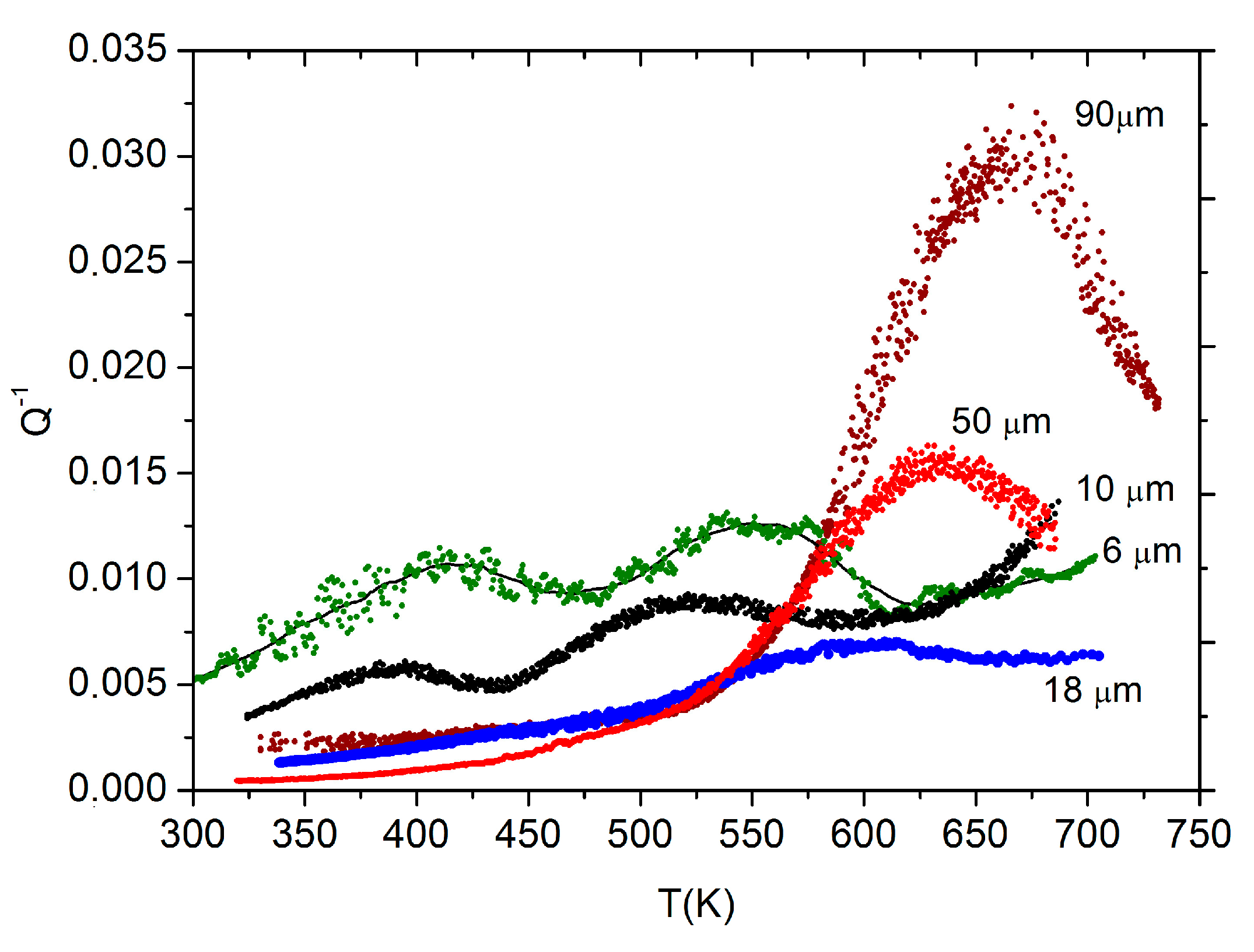
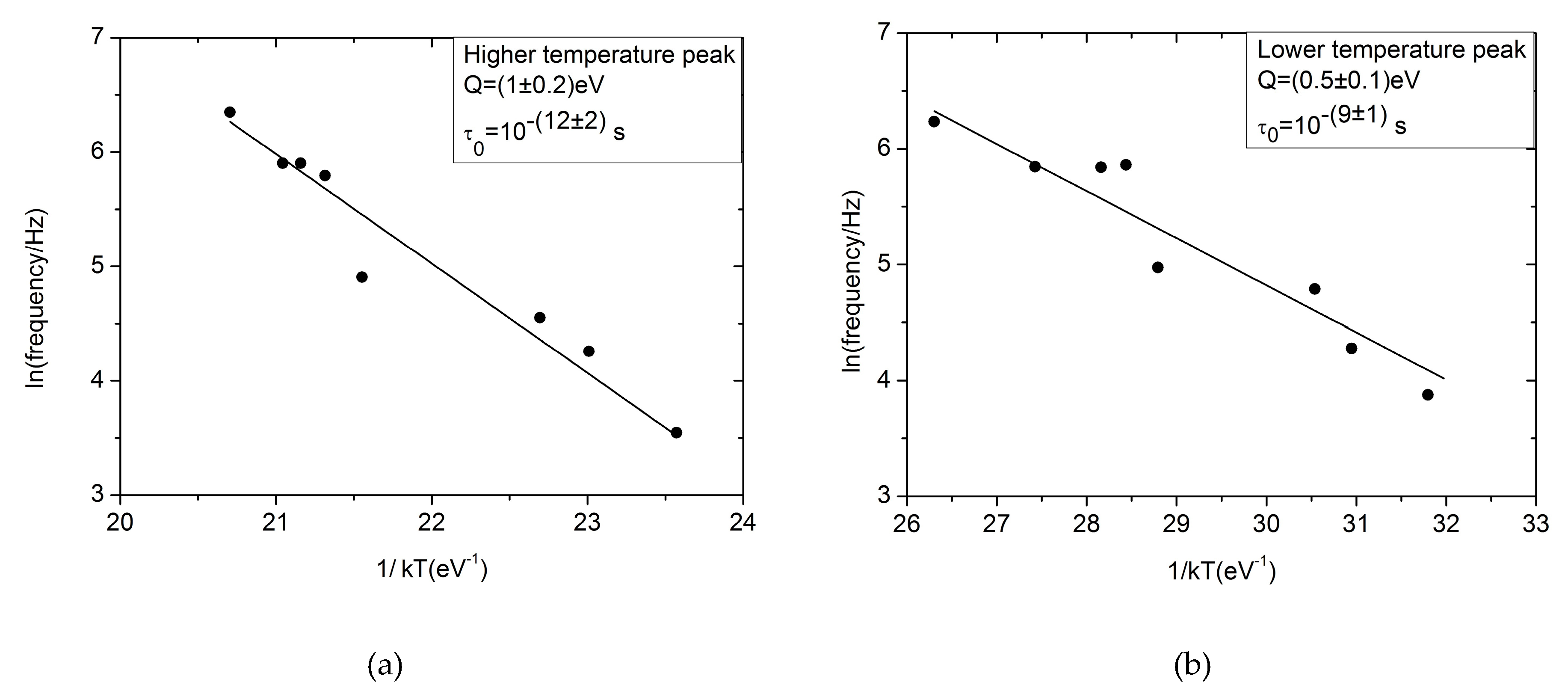
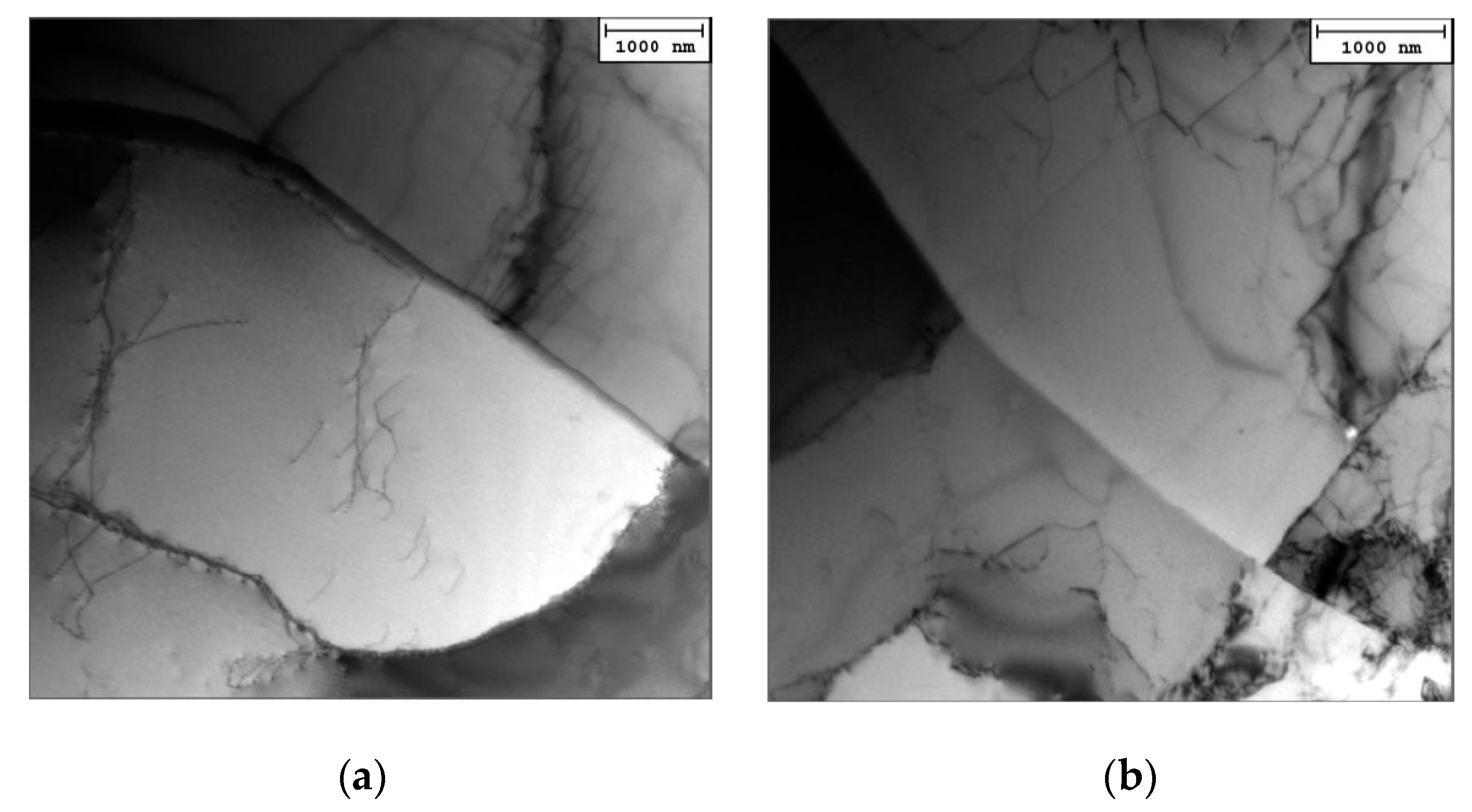
3. Results and Discussion

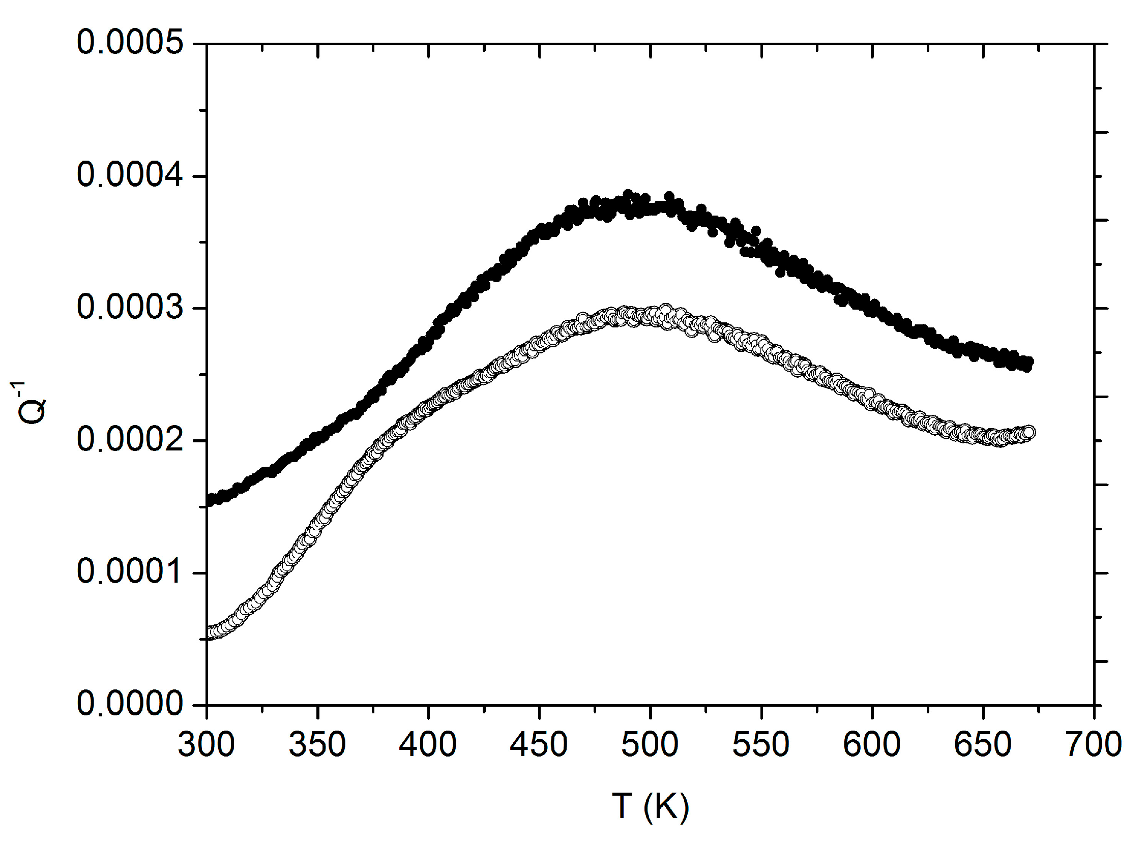
3.1. Deposited Films

Figure 2 shows typical Q−1 vs. temperature curves of films with thicknesses of 0.2 and 1 µm deposited on a silicon substrate.
These raw data can be analyzed in terms of a substrate contribution plus a film contribution. The substrate contribution can be subtracted using the equation [11]:
Q f 1 = Q c 1 + ( 1 / ( φ 1 ) ) [ Q c 1 Q s 1 ]
where the subscripts f, c and s refer to film, composite and substrate, respectively, and φ is:
φ = [ ( f c 2 l c 4 ) / ( f s 2 l s 4 ) ] [ 1 + ( ρ f t f / ρ s t s ) ] ,
where l, t, ρ, and f refer to the length, thickness, density and resonance frequency of the specimen.
As shown in Figure 3, Figure 4 and Figure 5, after the subtraction of the substrate contribution, the experimental data can be fitted as the sum (red curve) of an increasing exponential background (dark green curve), and two peaks with activation energies of 0.51 eV and 0.56 eV (green and blue curves), i.e., the same as those determined by Berry [11]. The peaks were assumed to be Debye peaks described by the relationship:
Q 1 = Δ sech [ ( H R ) ( 1 T 1 T p ) ] ,
where Δ is the relaxation strength, H the activation energy, R the gas constant and Tp the peak position. Each peak position Tp depends on the relaxation time τ0 and activation energy H:
ω τ 0 e H R T = 1
where ω = 2πf (f refers to resonance frequency).
To fit the experimental data in Figure 3, Figure 4 and Figure 5, the peak activation energies of the two peaks are fixed while the relaxation times and relaxation strengths are determined by the fit procedure. The different positions of the two peaks depend on different relaxation times, which are 4 × 10⁻¹¹ s and 6 × 10⁻¹⁰ s for the 0.2 µm specimen, and 9 × 10⁻¹¹ s and 1.4 × 10⁻⁹ s for the 0.4 µm and 1 µm specimens. The values of the relaxation times reported by Berry for 0.1 µm thick films are 4 × 10⁻¹³ s and 6 × 10⁻¹⁰, which are compatible with those found by us.
As expected, the peak relaxation strengths depend on film thickness and the two peaks, which are well separated in the thinnest specimen (0.1 µm), merge progressively as film thickness is increased (see Figure 4; Figure 5). This dependence of the peak’s position on thickness could perhaps explain the discrepancy between measurements by different research groups using a limited specimen thickness range.

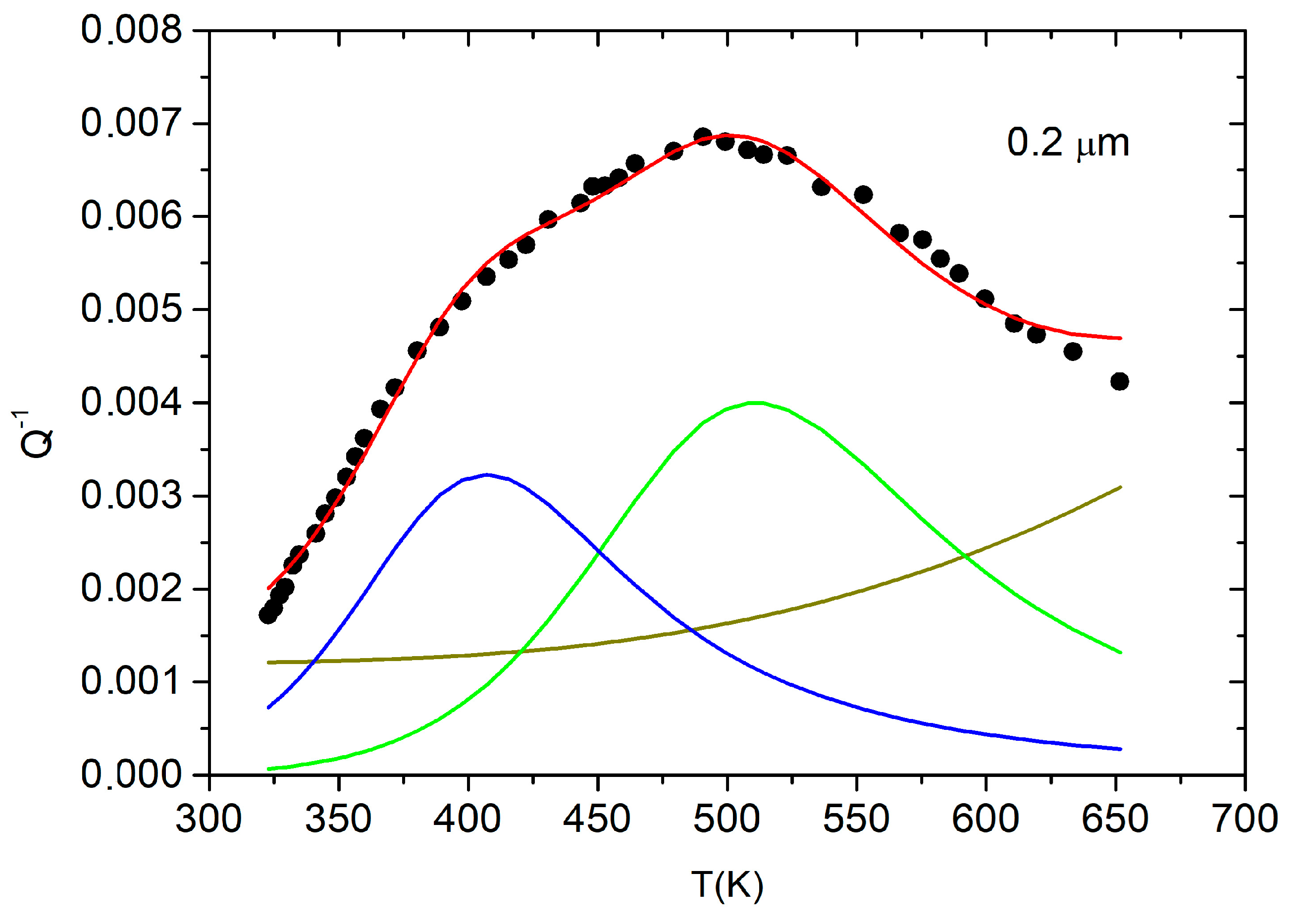
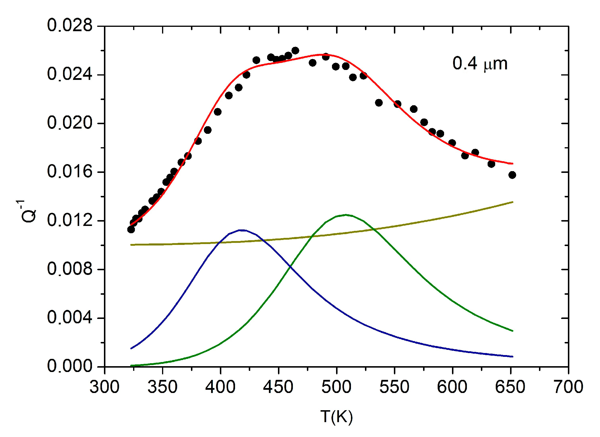
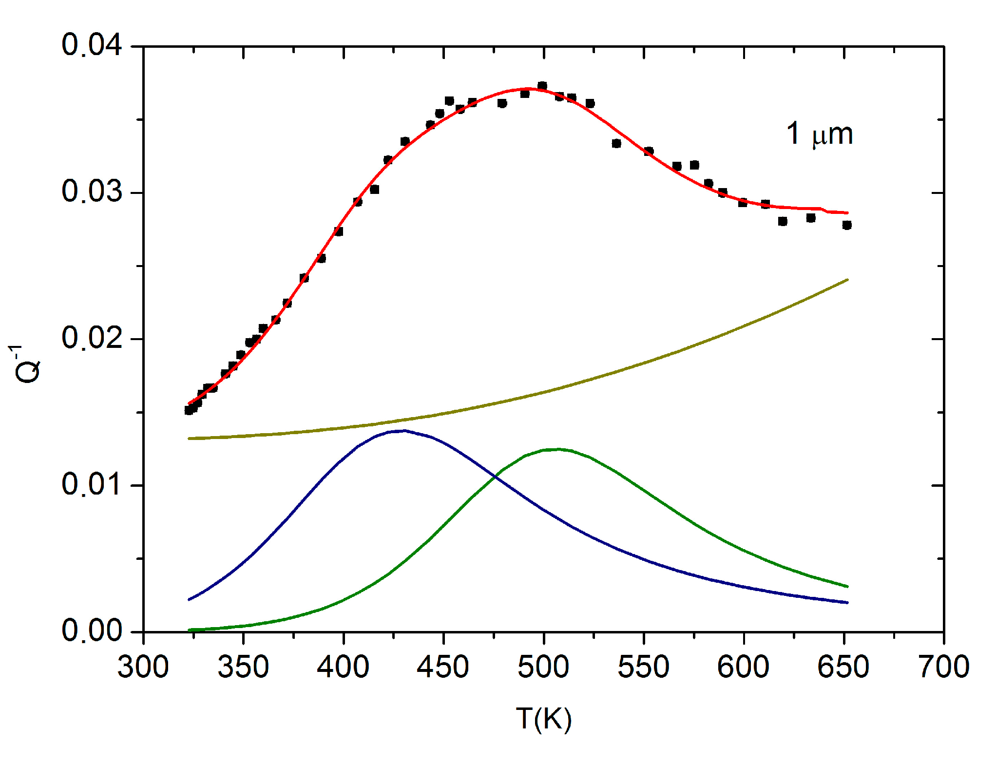
3.2. Free-Standing Films

Free-standing aluminum specimens of several thicknesses were measured and the results are shown in Figure 6. The bulk specimens exhibit the expected grain boundary peak, which at a resonance frequency of 250 Hz is located around 670 K. As the thickness of the cold-rolled specimens decreases, the peak progressively shifts to lower temperatures and a second peak is detected for thicknesses below or equal to 18 µm. In the same thin specimens, the background damping at temperatures below 500 K is higher compared to that of the thicker specimens.
The thermal stabilization at 700 K before tests greatly reduces the background damping of bulk specimens, which at 300 K becomes of the order of 1 × 10⁻³, namely ~0.2 that of the 10 µm thick specimens. In addition, when thickness is below 10 µm, the realization of MS measurements becomes difficult because the films exhibit a tendency to curl [19] and dynamic modulus shows a spurious increase with temperature.
The activation energies of the two peaks at lower and higher temperatures were determined by performing tests with different resonance frequencies. For example, the Arrhenius plots for the two peaks detected in the 10 µm thick specimens are reported in Figure 7a,b. The measured activation energy of the higher temperature peak is 1.0 ± 0.2 eV with a relaxation time τ0 = 10(−12±2) s. This is lower than the values obtained for the bulk specimens (thickness ≥ 50 µm) and those reported in literature [19,21], and it is compatible with pipe diffusion (0.85 eV [26]).
The activation energy of the lower temperature peak resulted was 0.5 ± 0.1 eV and the relaxation time τ0 = 10(−9±2) s.
The appearance of a second peak in free-standing specimens cannot obviously be attributed to any kind of film-substrate interaction. Its origin could be due to the restrained motion of dislocations arising when the specimen thickness becomes comparable to the size of the grains. The effects on damping of variations in grain size and in boundary sliding viscosity, which can easily occur in very thin cold-rolled specimens, have been simulated by Lee [27], who showed how peak weakening and broadening take place resulting in the possible appearance of two peaks.
Among all metals, aluminum has the highest stacking fault energy (~160 mJ/m2), thus cross-slip easily occurs in bulk specimens giving rise to cells and subgrains. Free dislocations inside the grains are commonly found at very low density.
The peak at lower temperature has an activation energy consistent with that of grain boundary diffusion (0.55 eV), as measured by Levenson in thin films [28]. The peak at higher temperature could be due to a phenomenon with a higher activation energy, namely the diffusion along dislocations (pipe diffusion, with an activation energy of 0.85 eV). In this case, it can be assumed that cross-slip is hindered by surface effects and that dislocations experience a progressive difficulty in forming subgrains as the thickness of the specimen decreases until it becomes comparable to the grain size. Therefore, in very thin specimens it is possible to find free dislocations in densities much higher than in bulk specimens. This could explain the appearance of a second peak with pipe diffusion activation energy. The hypothesis is supported by TEM observations. For example, Figure 8a, and 8b shows two micrographs of a 10 µm thick specimen which evidence a structure without well-defined cells and with dislocations not organized inside the grains.

4. Conclusions

Pure 99.999% (5 N) aluminum thin films, either deposited on silica substrates or as free-standing sheets obtained by cold rolling, were investigated by MS tests.
In both types of samples, anelastic phenomena are affected by the specimen thickness when it becomes comparable to grain size. Different phenomena occur and MS provided useful information through the analysis of peak activation energy.
The Q−1 vs. temperature curves of the deposited films can be fitted by two peaks with the same activation energies (0.51 eV and 0.56 eV) as those determined by Berry. The peak positions become progressively narrower as specimen thickness increases above 0.2 µm and the peaks tend to merge into a single peak.
Two peaks were also observed by examining the free-standing specimens. In this case, the high temperature peak, which appears below a critical specimen thickness of about 20 µm, has an activation energy (1.0 ± 0.2 eV) consistent with pipe diffusion and can be ascribed to free dislocations present at a higher density than in bulk specimens.

Author Contributions

All the authors discussed and planned the experiments; E.B., S.A. and E.G.C. performed MS tests; R.B. carried out TEM observations; R.M. contributed to the analysis of the results and the writing of the manuscript.

Funding

This research received no external funding.

Conflicts of Interest

The authors declare no conflict of interest.

References

  1. Uchic, M.D.; Dimiduk, D.M.; Florando, J.N.; Nix, W.D. Specimen dimensions influence strength and crystal plasticity. Science 2004, 305, 986–989. [Google Scholar] [CrossRef] [PubMed]
  2. Arzt, E. Size effects in materials due to microstructural and dimensional constraints: A comparative review. Acta Mater. 1998, 46, 5611–5626. [Google Scholar] [CrossRef]
  3. Kalman, A.J.; Verbruggen, A.H.; Janssen, G.C.A.M. Young’s modulus measurements and grain boundary sliding in free-standing thin metal films. Appl. Phys. Lett. 2001, 78, 2673. [Google Scholar] [CrossRef]
  4. Molotnikov, A.; Lapovok, R.; Davies, H.J.; Cao, C.W.; Estrin, Y. Size effect on the tensile strength of fine-grained copper. Scr. Mater. 2008, 9, 1182–1185. [Google Scholar] [CrossRef]
  5. Wei, X.; Lee, D.; Shim, S.; Chen, X.; Kysar, J.W. Plane-strain bulge test for nanocrystalline copper thin films. Scr. Mater. 2007, 57, 541–544. [Google Scholar] [CrossRef]
  6. Michel, J.F.; Picart, P. Size effects on the constitutive behaviour for brass in sheet metal forming. J. Mater. Proc. Technol. 2003, 141, 439–446. [Google Scholar] [CrossRef]
  7. Li, Q.; Anderson, P.M. Dislocation-based modeling of the mechanical behavior of epitaxial metallic multilayer thin films. Acta Mater. 2005, 53, 1121–1134. [Google Scholar] [CrossRef]
  8. Hosseini, E.; Kazeminezhad, M. A Dislocation-Based Model Considering Free Surface Theory Through HPT Process: Nano-Structured Ni. Trans. F: Nanotechnol. 2010, 17, 52–59. [Google Scholar]
  9. Baker, S.P.; Vinci, R.P.; Arias, T. Elastic and Anelastic Behavior of Materials in Small Dimensions. MRS Bull. 2002, 27, 26–29. [Google Scholar] [CrossRef]
  10. Berry, B.S.; Pritchet, W.C. Defect study of thin layers by the vibrating-reed technique. J. de Physique C5 1981, 42, 1111–1122. [Google Scholar] [CrossRef]
  11. Berry, B.S. Anelastic Relaxation and Diffusion in Thin-Layer Materials. In Diffusion Phenomena in Thin Films and Microelectronic Materials; Gupta, D., Ho, P.S., Eds.; Noyes Press: Park Ridge, NJ, USA, 1988; pp. 73–145. [Google Scholar]
  12. Bonetti, E.; Campari, E.G.; Enzo, S.; Groppelli, S.; Frattini, R.; Sberveglieri, G. Anelasticity and structural transformations of Fe and Al thin films and multilayers. Defect Diffus. Forum 1994, 106–107, 1–5. [Google Scholar] [CrossRef]
  13. Berry, B.S. Damping Mechanisms in Thin-Layer Materials. In M3D: Mechanics and Mechanisms of Material Damping; Kinra, V.K., Wolfenden, A., Eds.; ASTM STP 1169: Conshohocken, PA, USA, 1992; pp. 28–44. [Google Scholar]
  14. Prieler, M.; Bohn, H.G.; Schilling, W.; Trinkaus, H. Mat. Grain Boundary Sliding in Thin Substrate-Bonded AL Films. MRS Proc. 1993, 308, 305. [Google Scholar] [CrossRef]
  15. Prieler, M.; Bohn, H.G.; Schilling, W.; Trinkaus, H. Grain boundary sliding in thin substrate-bonded Al films. J. Alloys Compd. 1994, 211–212, 424–427. [Google Scholar] [CrossRef]
  16. Bohn, H.G.; Prieler, M.; Su, C.M.; Trinkaus, H.; Schilling, W. Internal friction effects due to grain boundary sliding in large- and small-grained aluminium. J. Phys. Chem. Solids 1994, 55, 1157–1164. [Google Scholar] [CrossRef]
  17. Heinen, D.; Bohn, H.G.; Schilling, W. Internal friction in free-standing thin Al films. J. Appl. Phys 1995, 78, 893–896. [Google Scholar] [CrossRef]
  18. Kê, T.S. Experimental evidence on the viscous behaviour of grain boundaries in metals. Phys. Rev. 1947, 71, 533–546. [Google Scholar] [CrossRef]
  19. Kong, Q.P.; Fang, Q.F. Progress in the investigations of grain boundary relaxation. Crit. Rev. Solid State Mater. Sci. 2016, 41, 192–216. [Google Scholar] [CrossRef]
  20. Jiang, W.B.; Kong, Q.P.; Magalas, L.B.; Fang, Q.F. The Internal Friction of Single Crystals, Bicrystals and Polycrystals of Pure Magnesium. Arch. Metall. Mater. 2015, 60, 371–375. [Google Scholar] [CrossRef] [Green Version]
  21. Kê, T.S.; Cui, P. Effect of solute atoms and precipitated particles on the optimum temperature of the grain boundary internal friction peak in Aluminum. Scr. Metall. Mater. 1992, 26, 1487. [Google Scholar]
  22. Choi, D.-h.; Kim, H.; Nix, W.D. Anelasticity and Damping of Thin Aluminum Films on Silicon Substrates. J. Microelectromech. Syst. 2004, 13, 230–237. [Google Scholar] [CrossRef]
  23. Nishino, Y. Mechanical Properties of Thin-Film Materials evaluated from Amplitude-Dependent Internal Friction. J. Electron. Mater. 1999, 28, 1023–1030. [Google Scholar] [CrossRef]
  24. Sosale, G.; Almecija, D.; Das, K.; Vengallatore, S. Mechanical spectroscopy of nanocrystalline aluminum films: effects of frequency and grain size on internal friction. Nanotechnology 2012, 23, 155701–155707. [Google Scholar] [CrossRef] [PubMed]
  25. Bonetti, E.; Campari, E.G.; Pasquini, L.; Savini, L. Automated resonant mechanical analyzer. Rev. Sci. Instr. 2001, 72, 2148. [Google Scholar] [CrossRef]
  26. No, M.L.; Esnouf, C.; San Juan, J.; Fantozzi, G. Dislocation motion in pure aluminium at 0.5 Tf: analysis from internal friction measurements. J. de Phys. 1985, 46, 347–350. [Google Scholar]
  27. Lee, L.C.S.; Morris, J.S. Anelasticity and grain boundary sliding. Proc. R. Soc. A 2010, 466, 2651–2671. [Google Scholar] [CrossRef] [Green Version]
  28. Levenson, L.L. Grain boundary diffusion activation energy derived from surface roughness measurements of aluminum thin films. Appl. Phys. Lett. 1989, 55, 2617–2619. [Google Scholar] [CrossRef]
Figure 1. Aluminum film deposited on a silicon substrate. The film thickness on each side ranges from 0.1 µm to 4 µm while the silicon substrate is 56 µm.
Metals 09 00549 g001
Figure 2. Q−1 vs. temperature curves of films deposited on a silicon substrate with thicknesses of 0.2 µm (open symbols) and 1 µm (solid symbols).
Metals 09 00549 g002
Figure 3. Q−1 vs. temperature curve of a 0.2 µm thick film deposited on a silicon substrate after the subtraction of the substrate contribution. Experimental data are fitted as the sum (red curve) of an increasing exponential background (dark green curve), and two peaks with activation energies of 0.51 eV and 0.56 eV (green and blue curves) [11].
Metals 09 00549 g003
Figure 4. Q−1 vs. temperature curve of a 0.4 µm thick film deposited on a silicon substrate after the subtraction of the substrate contribution. Experimental data are fitted as the sum (red curve) of an increasing exponential background (dark green curve), and two peaks with activation energies of 0.51 eV and 0.56 eV (green and blue curves) [11].
Metals 09 00549 g004
Figure 5. Q−1 vs. temperature curve of a 1 µm thick film deposited on a silicon substrate after the subtraction of the substrate contribution. Experimental data are fitted as the sum (red curve) of an increasing exponential background (dark green curve), and two peaks with activation energies of 0.51 eV and 0.56 eV (green and blue curves) [11].
Metals 09 00549 g005
Figure 6. Q−1 vs. temperature curves of free-standing specimens with thicknesses of 90 µm (magenta), 50 µm (red), 18 µm (blue), 10 µm (black), and 6 µm (green). The black line is just a guide for the eye. Resonance frequencies are about 250 Hz.
Metals 09 00549 g006
Figure 7. Aluminum specimens of 10 µm thickness. Arrhenius plots are shown for the peaks at higher temperature (a) and at lower temperature (b).
Metals 09 00549 g007
Figure 8. Aluminum specimen of 10 µm thickness. TEM observations of the grain and dislocation structure. (a,b) refers to different regions of the same specimen.
Metals 09 00549 g008

