Article

Evaluation of Microstructures and Mechanical Properties of Sn-10Sb-Ni Lead-Free Solder Alloys with Small Amount of Ni Using Miniature Size Specimens

Graduate School of Science and Technology, Gunma University, Kiryu 376-8515, Japan
*
Author to whom correspondence should be addressed.
Metals 2019, 9(12), 1348; https://doi.org/10.3390/met9121348
Submission received: 8 November 2019 / Revised: 11 December 2019 / Accepted: 12 December 2019 / Published: 14 December 2019

Abstract

:
Sn-Sb-Ni solder alloy is expected to be used as a die-attach material for a next-generation power semiconductors in power module. The aim of this paper is to investigate the effects of the Ni content on microstructures, tensile, and fatigue properties of Sn-10Sb-xNi (x = 0.05, 0.10, 0.25, 0.50) (mass%) lead-free solder alloys using miniature size specimens. The Sn-10Sb-Ni solder alloys have the microstructure in which Sb-Sn and Ni-Sb compounds are dispersed in the β-Sn matrix. As the Sb and Ni content increases, Sb-Sn and Ni-Sb compounds are coarsened, respectively. The effect of the Ni content on tensile properties of the alloy is slight at 25 °C. At 150 °C and 200 °C, 0.1% proof stress and tensile strength increase gradually with the Ni content increases, and saturate at the Ni amount over 0.25 mass%. According to the fatigue test at 200 °C, the fatigue properties of Sn-10Sb-Ni with 0.10–0.25 mass% Ni are better than that of the Sn-10Sb. From the experimental results, Sn-10Sb-Ni with 0.10–0.25 mass% Ni have superior mechanical properties.

1. Introduction

Power semiconductors are the key devices which control, convert, and supply electric power. They are used in the various fields such as automobiles, railway cars, machining tools, air conditioners, laptop computers, and so on to save energy. Si has typically been used as the material of the power semiconductors. Recently, next-generation power semiconductors such as SiC and GaN have been developed [1,2,3]. The next-generation power semiconductors make power electronics devices possible to operate at higher power levels and under high temperature environment [4,5]. On the other hand, it is essential for the practical use of the power electronics devices using the power semiconductors that power module components be withstood high heat environment. In particular, a die-attach material used between the power semiconductors and an insulated substrate such as Al2O3 and AlN requires both good tensile properties and high fatigue resistance [6,7]. In the present, Pb-rich solder alloys which is over 85 mass% Pb for high temperature environment are mainly used as the die-attach material despite Pb being toxic [8]. This is because high-temperature lead-free solder alloys have not been yet designated by the EU-RoHS directive. Therefore, the research and development of such solder alloys is required.
It is possible that the Sn-Sb solder alloys which have highest melting temperature range among existing lead-free solder alloys, are able to replace the Pb-rich solder alloys [7,8,9,10,11,12,13,14]. It has been reported that the Sn-Sb solder alloys have low electric resistivity and good mechanical properties [7,15]. However, in order to apply the Sn-Sb to the next-generation power semiconductors, it is necessary to further improve the tensile and fatigue properties in high temperature environment. Therefore, we focused on the Sn-Sb with Ni minor addition to further improve these properties. We have already reported that Sn-5Sb-Ni with 0.05–0.10 mass% Ni have superior fatigue properties to Sn-5Sb (mass%) in the temperature range from 25 °C to 200 °C [16]. In addition, it has been reported that the high concentration of Sb in the Sn-Sb solder alloys can increase mechanical strength [17,18,19]. In particular, Sn-10Sb (mass%) has been selected as another candidate together with the Sn-5Sb for previous studies [10,12,15,18].
The aim of this study was to investigate the effects of the Ni content on microstructures, tensile and fatigue properties of Sn-10Sb-Ni with 0.05–0.50 mass% Ni using miniature size specimens.

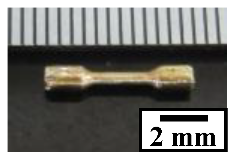
2. Materials and Methods

The ingots of Sn-10Sb-xNi (x = 0.05, 0.10, 0.25, 0.50) and Sn-10Sb solder alloys were prepared. On the basis of the differential scanning calorimetry (DSC) (DSC6200, Hitachi High-Tech Science, Inc., Tokyo, Japan) measurement result, the melting finish temperature of these solder alloys was estimated to be 247 °C for Sn-10Sb, 247 °C for Sn-10Sb-0.05Ni, and 246 °C for Sn-10Sb-0.50Ni. Therefore, these solders can be applied to high temperature applications with operating temperature up to 200 °C.
Miniature size specimens were made by casting from the ingots. First, a solder wire with 1.2 mm diameter was fabricated by drawing each ingot. Next, the solder wire inserted in the metal mold which made of aluminum alloy for making miniature size specimen [20]. Then they were put on a hot plate and the solder wire was pressed by the metal mold at casting temperature. Maximum casting temperature which was measured with a thermocouple attached to the surface of the metal mold was 264 °C for all solder alloys. Then the metal mold included the molten solder alloy was moved to a stainless plate for cooling. Maximum cooling rate was 3.6 °C/s on the stainless plate for the all solder alloys. Finally, a solder specimen was removed from the metal mold.
Figure 1 shows appearance of the miniature size specimen. The specimen gage length and diameter are 2.0 mm and 0.50 mm, respectively. The specimens were used for microstructure observation and mechanical properties test.
To observe the microstructures of miniature size specimens, cross-sectional polishing was conducted. The cross-sections of the specimens embedded in resin were polished by waterproof abrasive papers. Then, finish polishing was performed a using 1 µm diameter alumina powder. The microstructures of the cross-sections of the gauge regions were observed with an optical microscope and an electron probe X-ray microanalyzer (EPMA) (EPMA-1610, Shimadzu Corp., Kyoto, Japan). Moreover, the crystal orientations of the cross-sections of the gauge regions were investigated by a field emission scanning electron microscope (FE-SEM) (S-4300SE, Hitachi High-Tech Science, Inc., Tokyo, Japan) equipped with an electron back scattering diffraction (EBSD) (TSL MSC-2200, TexSEM Laboratories, Inc., Provo, UT, USA) system.
Table 1 shows the conditions of tensile test. The tests using the miniature size specimens were performed with a displacement controlled mechanical test system (LMH207-10, Saginomiya Seisakusho, Inc., Tokyo, Japan). The tests were conducted with five specimens per condition. After the tests, the appearance and fracture surface of specimens were observed with the EPMA.
Table 2 shows the conditions of fatigue test. The tests using the miniature size specimens were performed with the same equipment as the tensile tests. In each test, the continuous strain cycling of symmetrical triangle wave with a strain rate of 2.0 × 10⁻³ s−1 were conducted. In this study, the number of cycles to failure was defined as when the maximum load on the specimen dropped to 80%. After the tests, the crystal orientations and microstructures of the gauge regions were investigated by the FE-SEM equipped with the EBSD system.

3. Results and Discussion

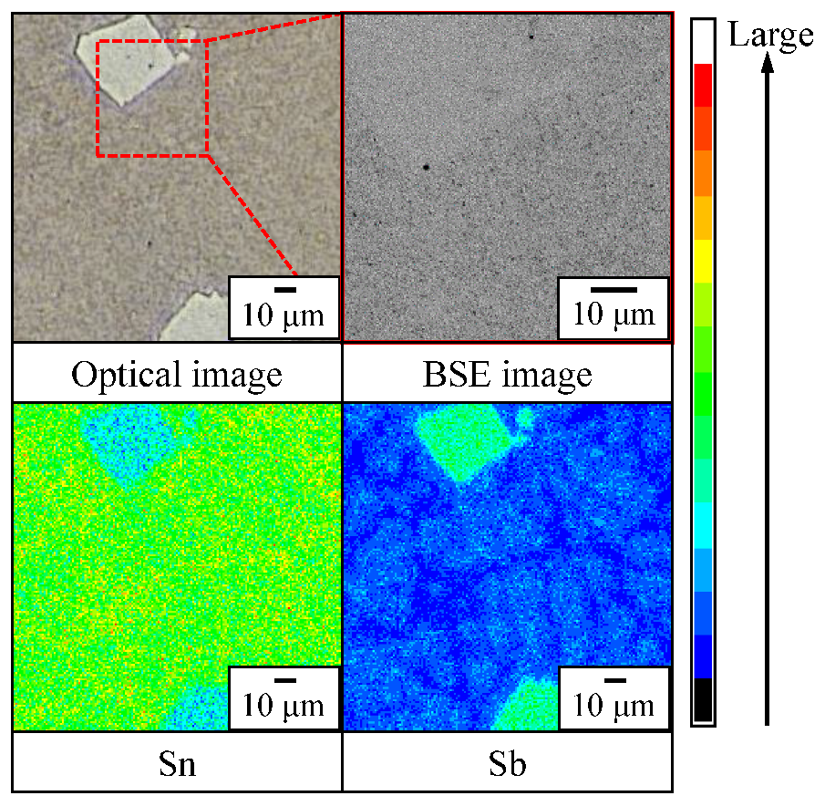
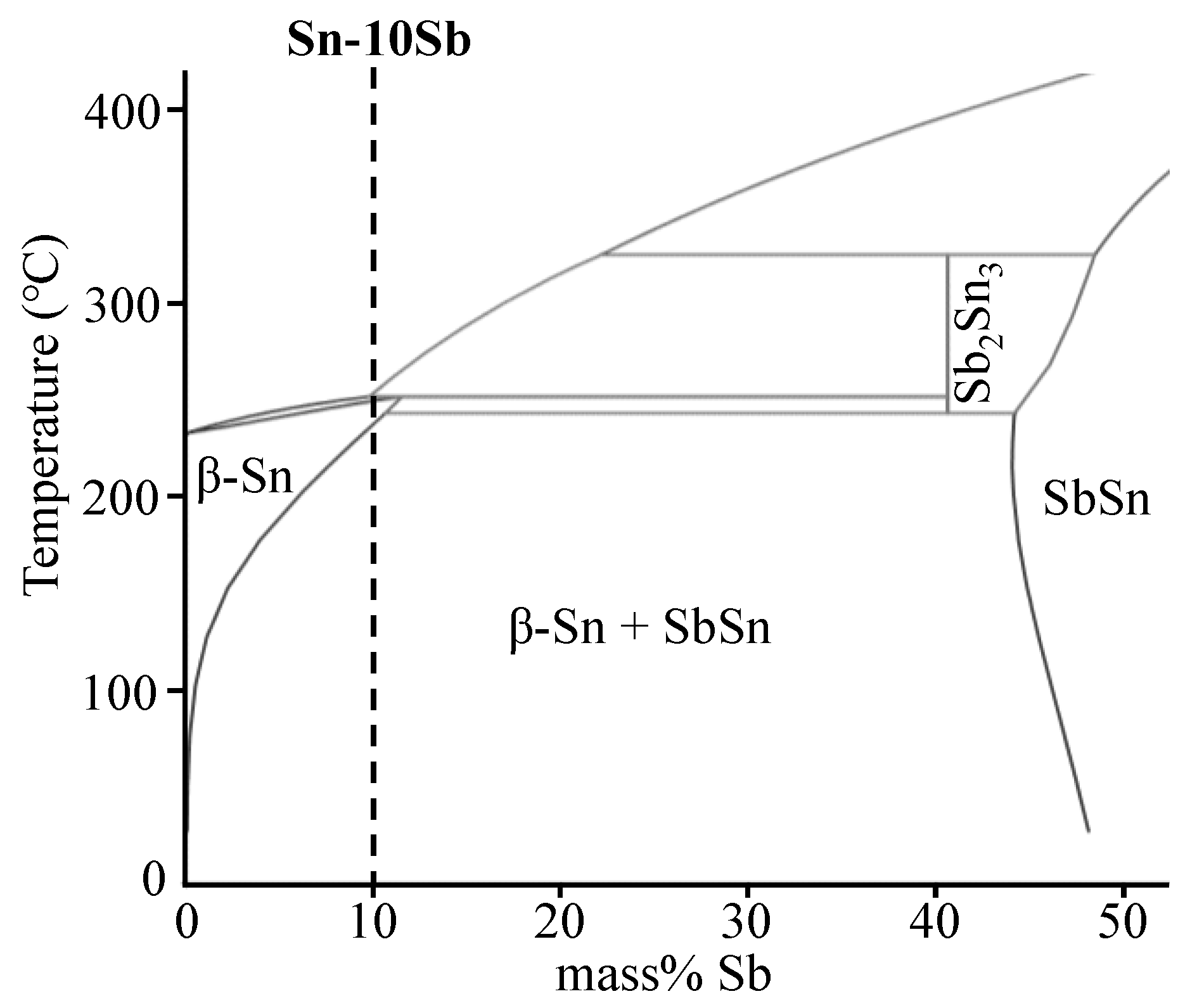
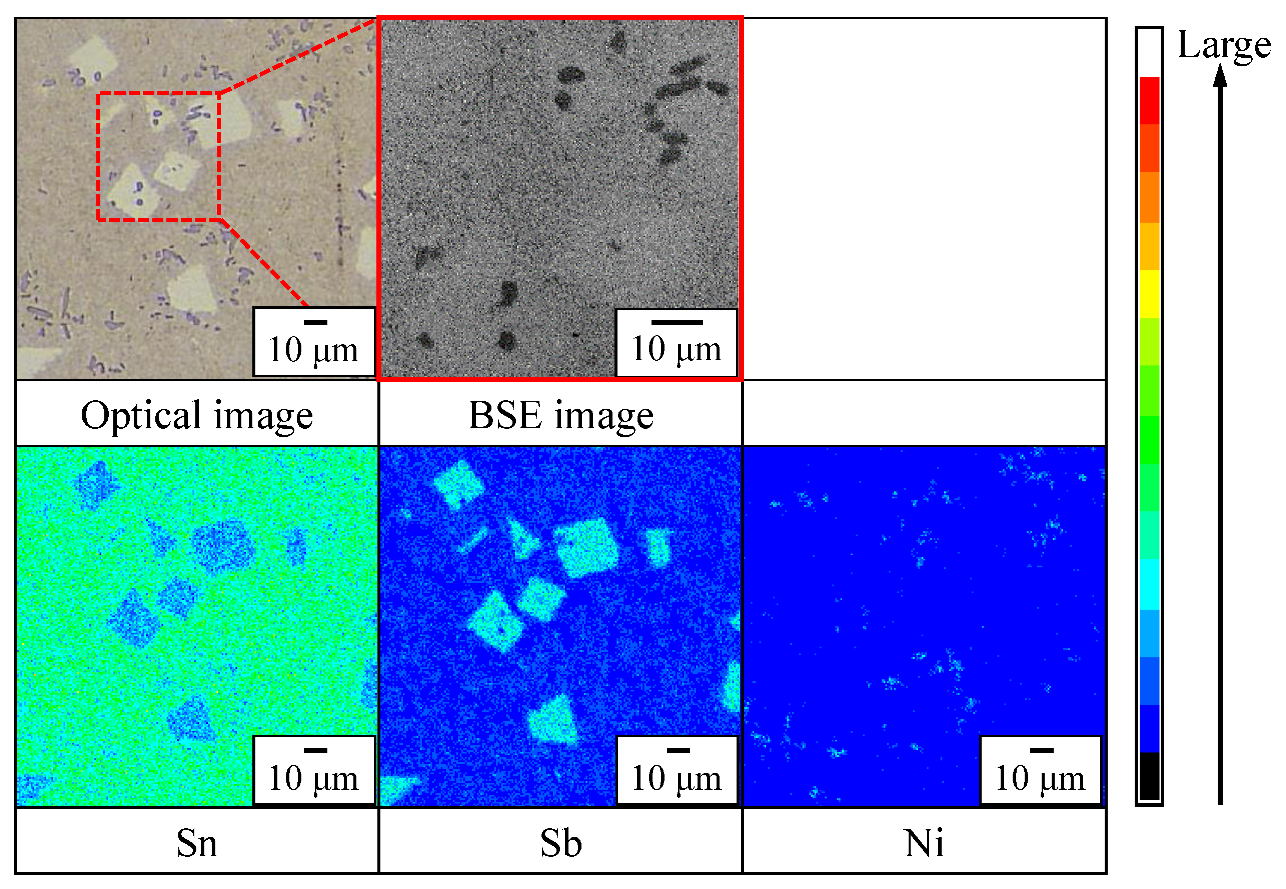
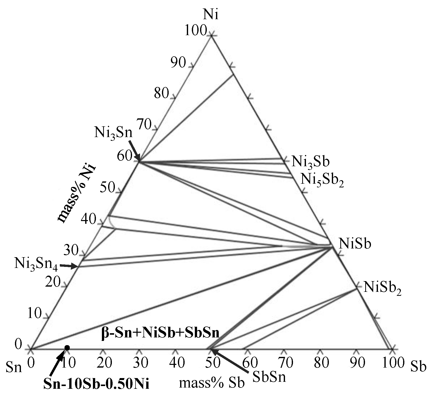
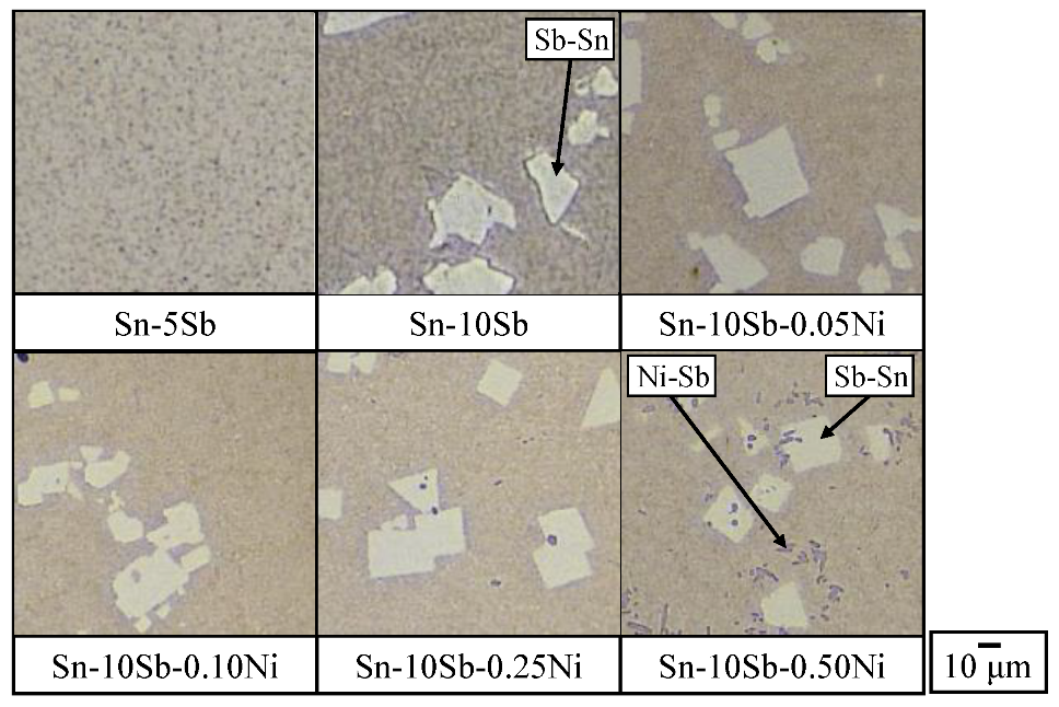
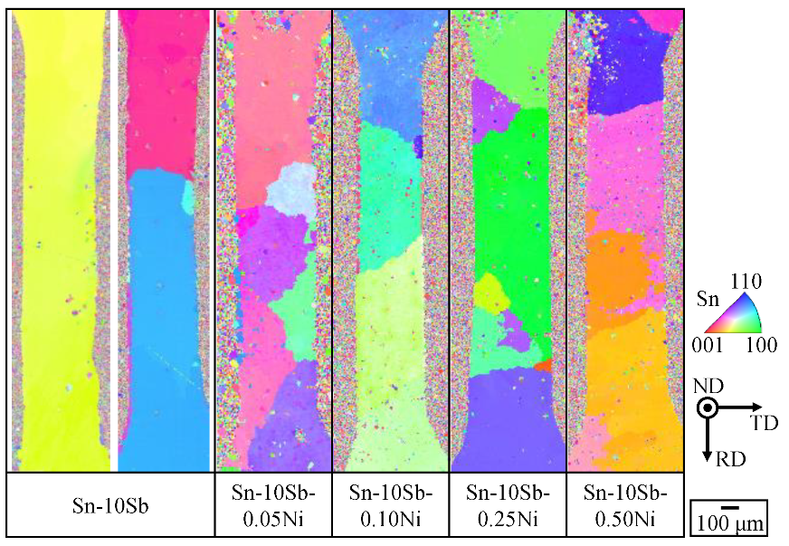
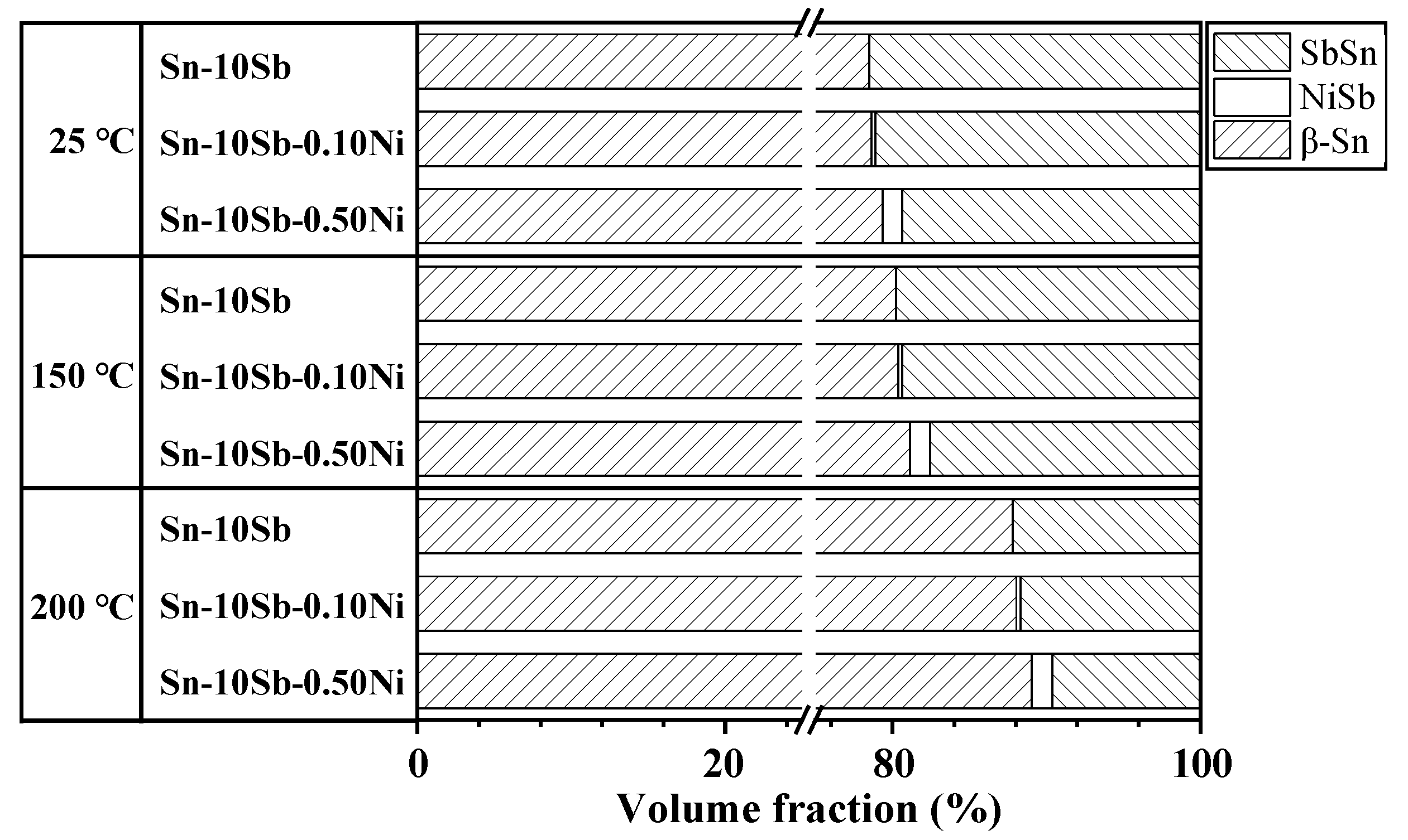
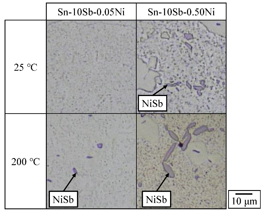
3.1. Microstructure Observation

Figure 2 shows the optical microscopy (OM) image of the cross-sectional view of as-cast Sn-10Sb specimen, the corresponding EPMA mapping analysis and the magnified backscattered electron (BSE) image. In the BSE image and its EPMA mapping analysis result, the two colors of dark-gray and bright-gray were observed and identified as Sn and Sn-Sb phases, respectively. Moreover, the distribution of block-shape particles with dozens of micrometers in size, was observed in the OM image. The particles were identified as Sn-Sb phases by EPMA mapping analysis.
Figure 3 shows the Sn-Sb binary equilibrium phase diagram that was created by thermodynamic calculation analysis (Thermo-Calc 2017a, Thermo-Calc Software Inc., McMurray, PA, USA). From the EPMA mapping analysis result and the diagram, the dark-gray phases in the BSE image were inferred to the β-Sn, and the bright-gray phases in the BSE image and the block-shape particles in the OM image are both inferred to the Sb-Sn phases. It has been reported that increasing Sb contents in Sn-Sb alloys causes the formation of coarsened Sb-Sn compounds [15,18]. Therefore, it was found that the Sn-10Sb has the microstructure in which fine and coarsened Sb-Sn compounds are dispersed in the β-Sn matrix.
Figure 4 shows the OM image of the cross-sectional view of as-cast Sn-10Sb-0.50Ni specimen, corresponding EPMA mapping analysis result and magnified BSE image. In the BSE image and the EPMA mapping analysis result, dark-gray, bright-gray and black phases were observed and identified as Sn, Sn-Sb, and Ni-Sb phases, respectively. Moreover, in the OM image, block-shape particles were observed as well as the Sn-10Sb, and identified as Sn-Sb phases by EPMA.
Figure 5 shows the Sn-Sb-Ni ternary equilibrium phase diagram at 25 °C. The composition point of Sn-10Sb-0.50Ni is also plotted in the diagram. From the EPMA mapping analysis result and the diagram, the dark-gray, bright-gray, and black phases in the BSE image were inferred to be the β-Sn, SbSn, and NiSb phases, respectively. Furthermore, the block-shape particles in the OM image were deduced to be the SbSn phases. Therefore, it was found that the Sn-10Sb-Ni solder alloys with 0.05–0.50 mass% Ni have the microstructure in which fine and coarsened Sb-Sn compounds and Ni-Sb compounds are dispersed in the β-Sn matrix.
Figure 6 shows the OM images of the cross-sectional views of the miniature size specimens of Sn-10Sb and Sn-10Sb-Ni with 0.05–0.50 mass%, and included that of Sn-5Sb [16] for comparison. As can be seen in the images, increasing the amount of Sb in the solder alloy coarsens Sn-Sb compounds. Moreover, increasing the amount of Ni in the solder alloy increases and coarsens Ni-Sb compounds.
Figure 7 shows the inverse pole figure (IPF) maps of the cross-sectional views of the miniature size specimens of Sn-10Sb and Sn-10Sb-Ni with 0.05–0.50 mass% Ni that were analyzed by the EBSD system. In this study, the longitudinal direction of the specimen was set to the rolling direction (RD) in the material coordinate system used in the EBSD system. In these images, different Sn grain orientations in the specimens are indicated by different colors. It was found that the specimen of Sn-10Sb consists of a single grain or a few grains, and specimens of Sn-10Sb-Ni consist of several grains.

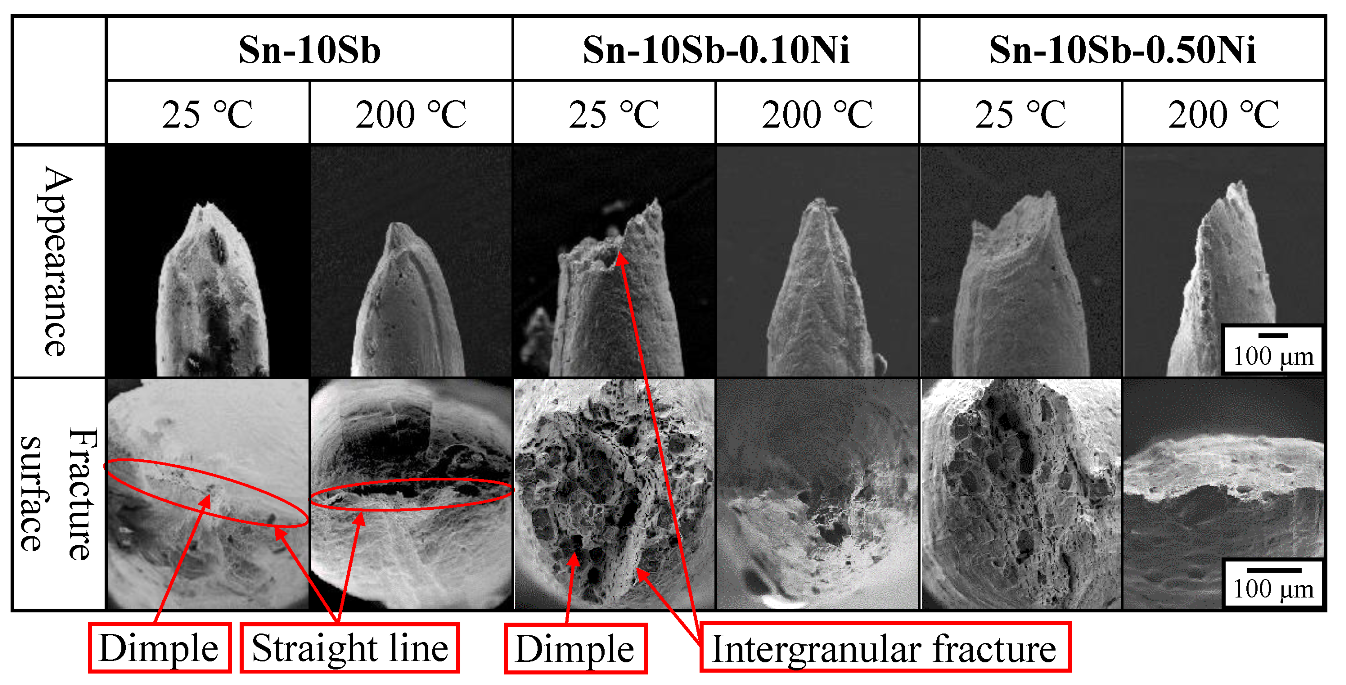
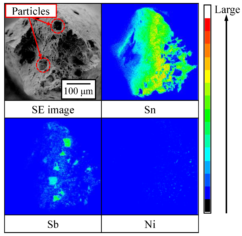
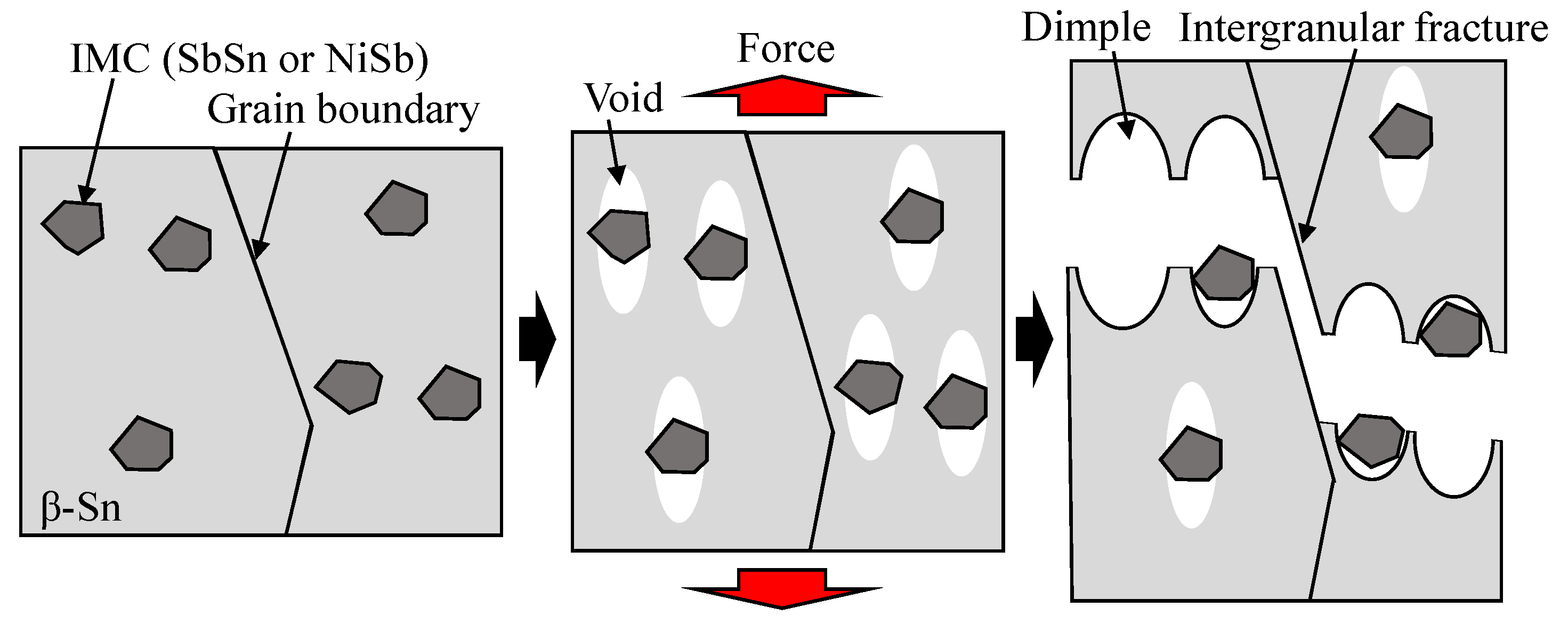
3.2. Tensile Properties and Fracture Modes

Figure 8 shows the measurement results of the tensile properties which are 0.1% proof stress, tensile strength and elongation of Sn-10Sb-Ni with 0.05–0.50 mass% Ni obtained by tensile test. These graphs contain results of Sn-10Sb for comparison. In the figure, the effects of the Ni content on the tensile properties was slight at 25 °C. We have reported that as the amount of Ni increases in Sn-5Sb-Ni with 0.05–0.50 mass%, the 0.1% proof stress and the tensile strength increase, and the elongation decreases at 25 °C [17]. This is because the dispersion strengthening is caused by Ni-Sb compounds. In this study, it seems that the tensile properties of the Sn-10Sb-Ni are largely influenced by the dispersion of the coarsened Sb-Sn compounds which do not exist in the Sn-5Sb-Ni. At 150 °C and 200 °C, the 0.1% proof stress and the tensile strength increased gradually with increasing the Ni content. However, they saturated at a Ni amount of 0.25 mass% or more. On the other hand, the elongation increased and decreased with inconsistent behavior regardless of the Ni content. According to the effects of temperature on the tensile properties, there is a tendency for the 0.1% proof stress and tensile strength to decrease as the temperature increases, but the elongation has a small effect.
Figure 9 shows the volume fractions of each phase in the Sn-10Sb, Sn-10Sb-0.10Ni, and Sn-10Sb-0.50Ni calculated by the thermodynamic calculation analysis. In the figure, the ratio of Sb-Sn phases decreases, that of β-Sn phases increases and that of Ni-Sb phases remains constant with an increase in temperature. Therefore, the reason why the 0.1% proof stress and tensile strength are increased by increasing the Ni content at high temperature is that the Sb-Sn compounds are decomposed and the dispersed Ni-Sb compounds have a significant effect.
Figure 10 shows the secondary electron (SE) images of fractured specimens after the tests. In the Sn-10Sb, fractured specimens exhibited chisel-point fracture. The fracture surface was shaped like knife-edge and formed some dimples. This means that ductile fractures occurred in the Sn-10Sb specimens. It has known that the slip system of β-Sn grain is limited by the anisotropy of Sn crystal orientation which has a body-centered tetragonal crystal structure [21]. The deformation and destruction are effected by limited slip system. As a result, the fracture specimen of Sn-based solder occurs chisel-point easily. In the Sn-10Sb-0.10Ni and Sn-10Sb-0.50Ni fractured specimens, dimples and intergranular fracture were observed at the fracture surfaces at 25 °C. Sn-10Sb-0.05Ni and Sn-10Sb-0.25Ni specimens also had a similar fractured surface. The intergranular fracture is the brittle fracture which the crack progress along a grain boundary. These specimens consisted of several grains as shown in the Figure 7, and thus the crack passed through the grain boundary on the way. At 150 °C and 200 °C, chisel-point fractures were observed. The others also had a similar fracture surface. The β-Sn melting temperature is 232 °C and is considerably elongated and deformed at high temperature, therefore chisel-point fracture easily occurs.
Figure 11 shows the SE image and its EPMA mapping analysis result of the fractured surface of a Sn-10Sb-0.50Ni specimen after the test. In the image, a plurality of particles were observed in the dimples. From the EPMA mapping analysis result, the particles were inferred to be Sb-Sn and Ni-Sb compounds.
Figure 12 shows the schematic diagrams of the formation mechanism of the dimples and intergranular fracture. During tensile deformation of Sn-10Sb-Ni specimen, voids are generated between the Sb-Sn and Ni-Sb compounds and the β-Sn matrix. This is because elastic modulus between the compounds and the matrix is different. Afterward, the voids become larger and combine each other, and eventually the specimen is broken. As a result, the dimples are formed on the fracture surface. If the specimen consists of several grains, crack passes through the grain boundary along the way. As a result, the intergranular fracture occurs.

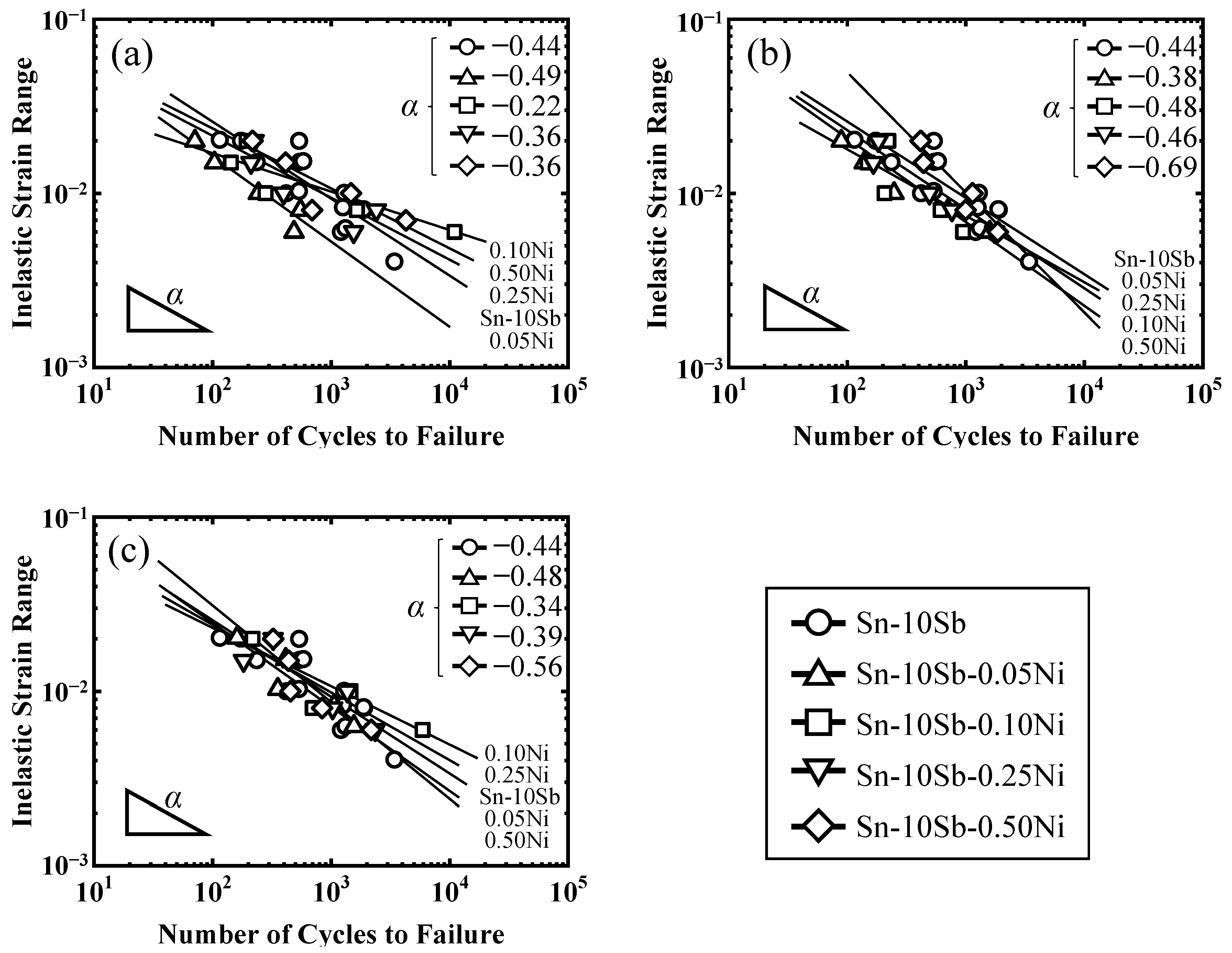
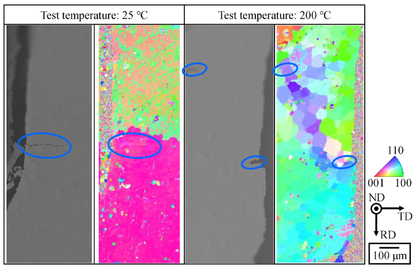
3.3. Fatigue Properties and Microstructural Change

Figure 13 shows the relationship between the inelastic strain range and the number of cycles to failure of the Sn-10Sb and Sn-10Sb-Ni with 0.05–0.50 mass% Ni specimens plotted on the double logarithm. In the graphs, Sn-10Sb and Sn-10Sb-Ni obey the Manson–Coffin equation as follows regardless of the temperature.
C = Δ ε in · N f α
where C is the fatigue ductility factor, Δεin is the inelastic strain range, Nf is the number of cycles to failure, and α is the fatigue ductility exponent. It has known that the low-cycle fatigue life of solder alloys generally obeys the Manson–Coffin equation [22,23,24,25].
The α is a slope of a linear line in the double logarithmic graphs showing a relationship between the Δεin and Nf. The lower the absolute values of α becomes, the better the fatigue properties obtain. At 25 °C, the absolute values of α of the Sn-10Sb-Ni solder alloys except for Sn-10Sb-0.05Ni were smaller than that of the Sn-10Sb. This means that these solder alloys have better fatigue properties than the Sn-10Sb. The α values of the Sn-10Sb-0.05Ni and Sn-10Sb were almost the same at 25 °C. At 150 °C and 200 °C, the absolute values of α values of the Sn-10Sb-Ni solder alloys except for the Sn-10Sb-0.05Ni tended to increase. This result has the same tendency as the fatigue properties of Sn-5Sb-Ni solder alloys that tested previously [16]. In particular, the absolute values of α of the Sn-10Sb-0.50Ni which has the most Ni addition was largest among all of the solder alloys in this study. The absolute values of α of the Sn-10Sb-0.05Ni were smaller than or almost the same to that of Sn-10Sb at 150 °C and 200 °C. Compared with the Sn-10Sb and Sn-10Sb-Ni, the absolute values of α of the Sn-10Sb-Ni with 0.05–0.25 mass% Ni were smaller or almost the same to that of the Sn-10Sb at high temperature. In particular, the fatigue properties of Sn-10Sb-0.10Ni and Sn-10Sb-0.25Ni are superior to the Sn-10Sb at 200 °C, which is the operating temperature of the next-generation power semiconductors.
Figure 14 shows the SE images and corresponding IPF maps of the cross-sectional views of Sn-10Sb-0.50Ni specimens after the tests at 25 °C and 200 °C. At 25 °C, a crack progress caused in a β-Sn grain. At 200 °C, the crack progress caused in fine crystal grain boundaries. It has been reported that local recrystallization process leads to the creation of fine β-Sn grains along a crack propagation path in the Sn-Ag-Cu solder alloys [26]. Therefore, it seems that the same phenomenon occurred in the Sn-Sb-Ni solder alloys.
Figure 15 shows OM images of the microstructures of the cross-sectional views of the specimens after the tests. In the Sn-10Sb-0.05Ni specimen, the sub-micrometer size particles of Ni-Sb compounds were observed at 25 °C. In the Sn-10Sb-0.50Ni specimen, the Ni-Sb compounds with 1–5 micrometer and sub-micrometer sizes were observed at 25 °C. The fine and coarsened Sb-Sn compounds also exist in the both solder alloys. It has been reported that the fine dispersoids which are at Sn grains with can suppress Sn grain growth after recrystallization as the pinning effect for dislocations [27]. In this study, it appears that dispersed fine Ni-Sb and Sb-Sn compounds in the solder alloy have the pinning effect and suppress local recrystallization process at 25 °C. As indicated previously, as the Ni content in the Sn-10Sb-Ni increases, the number of the Ni-Sb compounds increases. Therefore, the Sn-10Sb-Ni with the Ni amount of 0.10 mass% or more become small α values, and hence the solder alloys have superior fatigue properties at 25 °C. On the other hand, at 200 °C, the Ni-Sb compounds are coarsened to more 10 micrometer sizes in the Sn-10Sb-0.50Ni. Furthermore, the Sb-Sn compounds are decomposed as shown in Figure 9. Consequently, the absolute values of α of the solder alloy increased and the fatigue properties deteriorated. It seems that the pinning effect decreases because of the coarsened Ni-Sb compounds. Moreover, local recrystallization process is promoted due to deformation in the vicinity of the coarsened Ni-Sb compounds. In summary, it seems that the fatigue life decreased because the crack propagates easily to the fine β-Sn grain boundaries formed by local recrystallization process. On the other hand, in the Sn-10Sb-0.05Ni, the fine Ni-Sb compounds in the β-Sn matrix exist despite high temperature environment. Thus, stable fatigue properties can be obtained because local recrystallization process is suppressed.

4. Conclusions

In this study, the microstructure and mechanical properties of Sn-10Sb-xNi solder alloys (x = 0.05, 0.10, 0.25, 0.50 mass%) were investigated using miniature size specimens. The results of this study suggest the following conclusions:
(1)
The Sn-10Sb-Ni solder alloys with 0.05–0.50 mass% Ni have the microstructure in which Sb-Sn and Ni-Sb compounds are dispersed in β-Sn matrix. When Sb and Ni content in the Sn-Sb-Ni increases, the Sb-Sn and Ni-Sb compounds are coarsened, respectively.
(2)
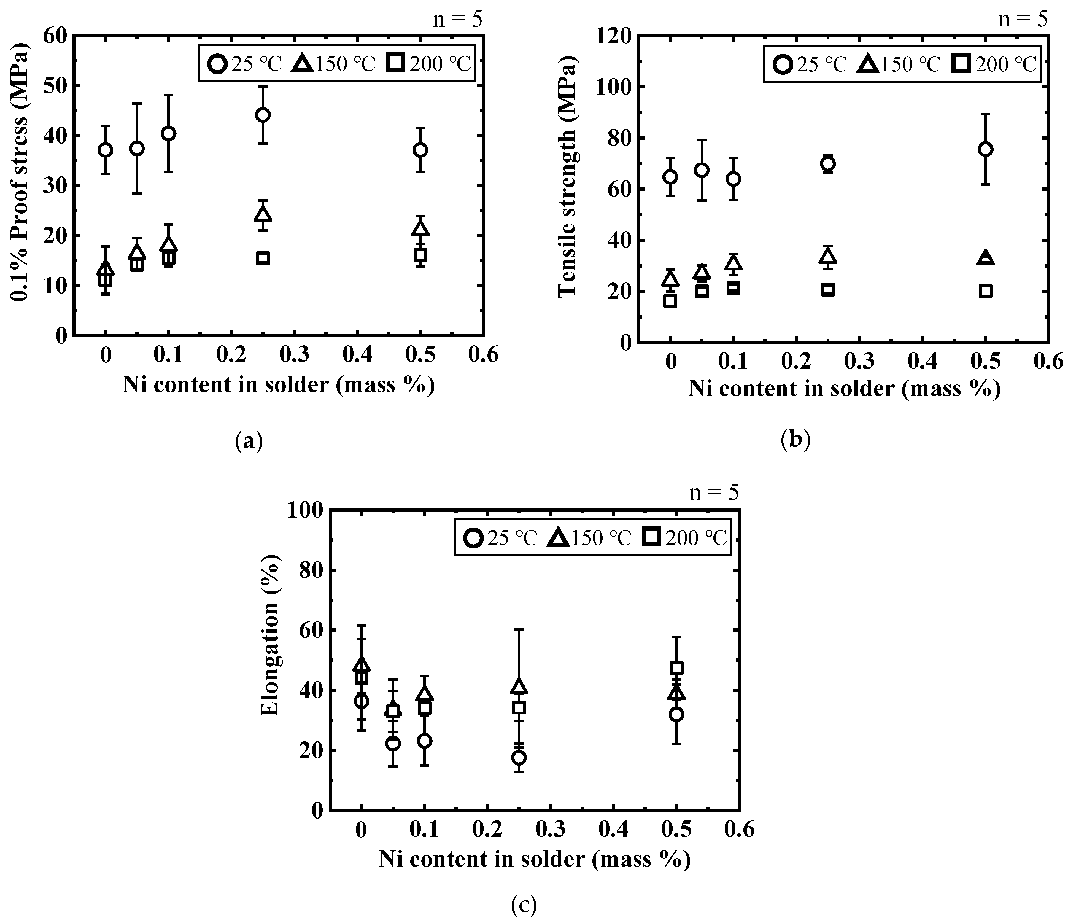
The effects of the Ni content on tensile properties of the Sn-10Sb-Ni solder alloys is slight at 25 °C. This is because the tensile properties are largely influenced by the dispersion of the coarsened SbSn compounds. At 150 °C and 200 °C, the 0.1% proof stress and the tensile strength increase gradually with the Ni content increase, and saturate at the Ni amount over 0.25 mass%. This is because the coarsened Sb-Sn compounds decompose and Ni-Sb compounds have a large effect on the tensile properties.
(3)
The absolute values of the fatigue ductility exponents α of the Sn-10Sb-Ni solder alloys are smaller than that of the Sn-10Sb except for Sn-10Sb-0.05Ni at 25 °C. At 150 °C and 200 °C, the absolute values of α of all of the Sn-10Sb-Ni increase except for the Sn-10Sb-0.05Ni. In particular, the absolute values of α of the Sn-10Sb-Ni solder alloys are smaller than that of the Sn-10Sb except for Sn-10Sb-0.05Ni at 25 °C. The absolute values of α of the Sn-10Sb-0.50Ni are larger than any other solder alloys. Compared with the Sn-10Sb and Sn-10Sb-Ni, the fatigue properties of Sn-10Sb-Ni solder alloys with 0.10–0.25 mass% Ni are better than that of Sn-10Sb at 200 °C.
(4)
In the Sn-10Sb-0.50Ni solder alloy, dispersed fine Ni-Sb compounds have the dislocation pinning effect and suppress local recrystallization process at 25 °C. However, at high temperature, the dislocation pinning effect decreases due to the formation of coarsened Ni-Sb compounds. Consequently, the fatigue life decreased because the crack propagates easily to the fine β-Sn grain boundaries formed by local recrystallization process.

Author Contributions

Conceptualization, T.K. and I.S.; methodology, I.S.; investigation, T.K.; data curation, T.K.; writing—original draft preparation, T.K.; writing—review and editing, T.K. and I.S.; supervision, I.S.

Funding

This research received no external funding.

Conflicts of Interest

The authors declare no conflict of interest.

References

  1. Matallana, A.; Ibarra, E.; Lopez, I.; Andreu, J.; Garate, J.I.; Jorda, X.; Rebollo, J. Power module electronics in HEV/EV applications: New trends in wide-bandgap semiconductor technologies and design aspects. Renew. Sustain. Energy Rev. 2019, 113, 109264. [Google Scholar] [CrossRef]
  2. Roccaforte, F.; Fiorenza, P.; Greco, G.; Nigro, R.L.; Giannazzo, F.; Iucolano, F.; Saggio, M. Emerging trends in wide band gap semiconductors (SiC and GaN) technology for power devices. Microelectron. Eng. 2018, 187–188, 66–77. [Google Scholar] [CrossRef]
  3. Mu, F.; Wang, Y.; He, R.; Suga, T. Direct wafer bonding of GaN-SiC for high power GaN-on-SiC devices. Materialia 2018, 3, 12–14. [Google Scholar] [CrossRef]
  4. Millan, J.; Godignon, P.; Perpina, X.; Perez-Tomas, A.; Rebollo, J. A survey of wide bandgap power semiconductor devices. IEEE Trans. Power Electron. 2014, 29, 2155–2163. [Google Scholar] [CrossRef]
  5. Hayato, N.; Yuichiro, H.; Masafumi, H. Ultra-compact, high-reliability all-SiC module. Fuji Electr. Rev. 2013, 59, 221–225. [Google Scholar]
  6. Suganuma, K.; Kim, S.J.; Kim, K.S. High-temperature lead-free solders: Properties and possibilities. JOM 2009, 61, 64–71. [Google Scholar] [CrossRef]
  7. Kobayashi, K.; Shohji, I.; Hokazono, H. Tensile and fatigue properties of miniature size specimens of Sn-5Sb lead-free solder. Mater. Sci. Forum 2016, 879, 2377–2382. [Google Scholar] [CrossRef]
  8. Rettenmayr, M.; Lambracht, P.; Kempf, B.; Graff, M. High melting Pb-free solder alloys for die-attach applications. Adv. Eng. Mater. 2005, 7, 965–969. [Google Scholar] [CrossRef]
  9. Dias, M.; Costa, T.; Rocha, O.; Spinelli, J.E.; Cheung, N.; Garcia, A. Interconnection of thermal parameters, microstructure and mechanical properties in directionally solidified Sn-Sb lead-free solder alloys. Mater. Charact. 2015, 106, 52–61. [Google Scholar] [CrossRef]
  10. Chen, Y.T.; Chen, C.C. Interfacial reactions in Sn-Sb/Ni couples. J. Taiwan Inst. Chem. Eng. 2012, 43, 295–300. [Google Scholar] [CrossRef]
  11. Lin, C.; Lee, C.; Liu, X.; Yen, Y. Phase equilibria of the Sn-Sb-Ag ternary system and interfacial reactions at the Sn-Sb/Ag joints at 400 °C and 150 °C. Intermetallics 2018, 16, 230–238. [Google Scholar] [CrossRef]
  12. Chen, S.W.; Zi, A.R.; Chen, P.Y.; Wu, H.J.; Chen, Y.K.; Wang, C.H. Interfacial reactions in the Sn-Sb/Ag and Sn-Sb/Cu couples. Mater. Chem. Phys. 2008, 111, 17–19. [Google Scholar] [CrossRef]
  13. Chen, S.W.; Chen, C.C.; Gierlotka, W.; Zi, A.R.; Chen, P.Y.; Wu, H.J. Phase equilibria of the Sn-Sb binary system. J. Electron. Mater. 2008, 37, 992–1002. [Google Scholar] [CrossRef]
  14. Corbin, S.F. High-temperature variable melting point Sn-Sb lead-free solder pastes using transient liquid-phase powder processing. J. Electron. Mater. 2005, 34, 1016–1025. [Google Scholar] [CrossRef]
  15. Kim, J.H.; Jeong, S.W.; Lee, H.M. Thermodynamics-aided alloy design and evaluation of Pb-free solders for high-temperature applications. Mater. Trans. 2002, 43, 1873–1878. [Google Scholar] [CrossRef] [Green Version]
  16. Kobayashi, T.; Mitsui, K.; Shohji, I. Effects of Ni addition to Sn-5Sb high-temperature lead-free solder on its microstructure and mechanical properties. Mater. Trans. 2019, 60, 888–894. [Google Scholar] [CrossRef] [Green Version]
  17. Kobayashi, T.; Kobayashi, K.; Mitsui, K.; Shohji, I. Comparison of Sn-5Sb and Sn-10Sb alloys in tensile and fatigue properties using miniature size specimens. Adv. Mater. Sci. Eng. 2018, 2018, 1416942. [Google Scholar] [CrossRef] [Green Version]
  18. Morozumi, A.; Hokazono, H.; Nishimura, Y.; Mochizuki, E.; Takahashi, Y. Influence of antimony on reliability of solder joints using sn-sb binary alloy for power semiconductor modules. Trans. Jpn. Inst. Electron. Packag. 2015, 8, 8–17. [Google Scholar] [CrossRef] [Green Version]
  19. Shohji, I.; Toyama, Y. Effect of strain rate on tensile properties of miniature size specimens of several lead-free alloys. Mater. Sci. Forum 2014, 783, 2810–2815. [Google Scholar] [CrossRef]
  20. Kariya, Y.; Niimi, T.; Suga, T.; Otsuka, M. Isothermal fatigue properties of Sn-Ag-Cu alloy evaluated by micro size specimen. Mater. Trans. 2005, 46, 2309–2315. [Google Scholar] [CrossRef] [Green Version]
  21. Telang, A.U.; Bieler, T.R. The orientation imaging microscopy of lead-free Sn-Ag solder joints. J. Miner. Met. Mater. Soc. 2005, 57, 44–49. [Google Scholar] [CrossRef]
  22. Takahashi, H.; Kawakami, T.; Mukai, M.; Ohno, N. Thermal fatigue life simulation for Sn-Ag-Cu lead-free joints. J. Jpn. Inst. Electron. Packag. 2004, 7, 308–313. [Google Scholar] [CrossRef]
  23. Kanchanomai, C.; Miyashita, Y.; Mutoh, Y. Low-cycle fatigue behavior of Sn-Ag, Sn-Ag-Cu, and Sn-Ag-Cu-Bi lead-free solders. J. Electron. Mater. 2002, 31, 456–465. [Google Scholar] [CrossRef]
  24. Lee, C.C.; Chang, K.C. Lead-free solder joint reliability estimation of flip chip package using FEM-based sensitivity analysis. Solder. Surf. Mt. Technol. 2009, 21, 31–41. [Google Scholar] [CrossRef] [Green Version]
  25. Pang, J.H.L.; Xiong, B.S.; Low, T.H. Low cycle fatigue study of lead free 99.3Sn-0.7Cu solder alloy. Int. J. Fatigue 2004, 26, 865–872. [Google Scholar] [CrossRef]
  26. Libot, J.B.; Alexis, J.; Dalverny, O.; Arnaud, L.; Milesi, P.; Dulondel, F. Microstructural evolutions of Sn-3.0Ag-0.5Cu solder joints during thermal cycling. Microelectron. Reliab. 2018, 83, 64–76. [Google Scholar] [CrossRef] [Green Version]
  27. Terashima, S.; Tanaka, M. Thermal fatigue properties of Sn-1.2Ag-0.5Cu-xNi flip chip interconnects. Mater. Trans. 2004, 45, 681–688. [Google Scholar] [CrossRef] [Green Version]
Figure 1. Appearance of miniature size specimen of solder alloy.
Metals 09 01348 g001
Figure 2. Optical microscopy (OM) image of microstructures of Sn-10Sb specimen, corresponding electron probe X-ray microanalyzer (EPMA) mapping analysis result and magnified backscattered electron (BSE) image.
Metals 09 01348 g002
Figure 3. Sn-Sb binary equilibrium diagram [16].
Metals 09 01348 g003
Figure 4. OM image of microstructures of Sn-10Sb-0.50Ni specimen, corresponding EPMA mapping analysis result and magnified BSE image.
Metals 09 01348 g004
Figure 5. Sn-Sb-Ni ternary equilibrium phase diagram at 25 °C, reprinted with permission from [16], copyright The Japan Institute of Metals and Materials.
Metals 09 01348 g005
Figure 6. OM images of microstructures of Sn-5Sb, Sn-10Sb, and Sn-10Sb-Ni specimens.
Metals 09 01348 g006
Figure 7. Inverse pole figure (IPF) maps of initial microstructures of Sn-10Sb and Sn-10Sb-Ni specimens.
Metals 09 01348 g007
Figure 8. Tensile properties of Sn-10Sb and Sn-10Sb-Ni with 0.05–0.50 mass% Ni. (a) 0.1% proof stress, (b) Tensile strength, and (c) Elongation.
Metals 09 01348 g008
Figure 9. Volume fraction of β-Sn, Ni-Sb, and Sb-Sn phases in Sn-10Sb, Sn-10Sb-0.10Ni, and Sn-10Sb-0.50Ni solder alloys by thermodynamic calculation analysis.
Metals 09 01348 g009
Figure 10. Secondary electron (SE) images of fractured specimens after tensile tests.
Metals 09 01348 g010
Figure 11. SE image of fractured surface of Sn-10Sb-0.50Ni and corresponding EPMA composition maps after tensile test (test temperature: 25 °C).
Metals 09 01348 g011
Figure 12. Schematic diagrams of formation mechanism of dimple and intergranular fracture.
Metals 09 01348 g012
Figure 13. Fatigue properties of Sn-10Sb and Sn-10Sb-Ni with 0.05–0.50 mass% Ni. (a) 25 °C, (b) 150 °C, and (c) 200 °C.
Metals 09 01348 g013
Figure 14. SE images and corresponding IPF maps of microstructures of Sn-10Sb-0.50Ni specimens after fatigue tests.
Metals 09 01348 g014
Figure 15. OM images of microstructures of Sn-10Sb-0.05Ni and Sn-10Sb-0.50Ni specimens after fatigue tests at ∆εt = 1.0%.
Metals 09 01348 g015
Table 1. Conditions of tensile test.
Temperature (°C)Strain Rate (s−1)
25, 150, 2002.0 × 10−1
Table 2. Conditions of fatigue test.
Temperature (°C)Strain Rate (s−1)Total Strain Range (%)
25, 150, 2002.0 × 10−30.4–2.0

