Abstract
The influence of electropulses in situ on the drawing process of copper wires was investigated, with the aim of avoiding time consuming annealing thermal treatments. It was found that with the application of electropulses, tensile and drawing forces were reduced and the plasticity of the wire was improved. Meanwhile, compared with conventional drawing, hardness decreased. With the electropulsing treatment, no differences were found in the material’s resistivity. The microstructure exhibited similar grain size despite the joule effect, although some changes were found in the low and high angle grain boundaries. Compressive residual stresses were found on the surface during the assisted process; consequently, these specimens were expected to have a better performance under fatigue fracture. Therefore, we have found the first evidence of the advantages of this hybrid technique for pure copper wire drawing and, ultimately, to replace the conventional drawing annealing process with a more time effective electropulse-assisted drawing process.
1. Introduction
Copper wires resulting from plastic deformation by the drawing process are widely available products in the manufacturing industry. When the copper wire is plastically deformed, its electrical conductivity decreases due to dislocation accumulation because of the hardening phenomenon. Thus, thermal treatment is necessary to increase the electrical conductivity and improve the plastic deformability of cooper wires for further drawing steps [1]. In the conventional cold wire drawing process (CD), annealing is used to reduce hardness and obtain uniformly distributed grain size [2]. Since it is a high cost and energy intensive technique, the present study explores the use of a non-conventional technology—plastic deformation assisted with electropulses—to make the whole drawing process more economical. The application of electropulsing treatment (EPT) can reduce the deformation hardening and save annealing procedures in cold drawing processing [3], where even weak electrical potentials have been proved to reduce the plasticity of pure copper [4].
In wire drawing of copper, the maximum equivalent strain increases due to the increase in friction forces that makes the deformation more inhomogeneous near to the die–wire interface, causing wire splitting [5]. Due to the application of EPT, the surface quality of wire improved and drawing stress decreased to about 50% compared with the CD process [6]. The plastic deformation induced by interaction forces between the die and wire influences the microstructure of deformed alloys, thus, it is necessary to reduce these stresses in order to achieve better mechanical properties and formability [7]. In EPT wire drawing processes, residual stresses can be completely removed or transformed to a more appropriate pattern by mechanical or thermal processes [8]. Manel et al. [9] suggested that tensile residual stresses could be reduced by bending the drawn wires at smaller radii and higher temperatures. Drawing stresses can also be decreased by applying current pulses in the deformation zone of drawing die, which significantly reduces the work hardening of wires [10]. Thus, due to a decrease in deformation resistance, the drawing forces decrease, and hence, ultimate tensile strength also reduces, which improves the plastic deformability of material and prolongs the service life of die [11]. Zimniak et al. [12] investigated the electroplastic effect in the cold drawing of copper wires and found that the drawing forces decreased and the plastic properties of wire improved with the application of EPT. Similarly, Troistskiy et at. [13] showed that, as compared to the CD process, wire plasticity was enhanced, and necessary drawing forces decreased by 30–35% and electrical resistance decreased by 18–20% during EPT of copper. Recently, Egea et al. [14] analyzed the effect of EPT on drawing forces, mechanical behavior, and the microstructure of the material. They observed that, as compared to the CD process, the microstructure of material changes through increasing the grain size and decreasing drawing forces, tensile strength, and the hardness of material during the EPT process. Following the aforementioned results, the present work focused on studying the effect of current pulses on drawing forces, residual stresses, resistivity and the hardness of pure copper wires during the drawing process. The microstructure of the material and deformation mechanism is also studied, in order to analyze the plasticity of wire. From a manufacturing point of view, the uncertainty of cost of an annealing treatment is the main challenge in the drawing process. Thus, using EPT to improve/maintain the wire quality (resistivity and residual stresses) and reduce the cost of copper wire, thereby avoiding the annealing treatment, is the ultimate objective of present work.
2. Methodology
Experimental Procedure
The wires of pure copper (99.99%), supplied by Prysmian Cables Spain S.A.U., Barcelona, Spain, used in the present work were provided by Prysmian group (Spain). The wire sample dimensions were 500 mm length and 150 mm of initial thread. The wire drawing process was performed with an Instron universal testing machine (model: 4206, Instron, Norwood, MA, USA) with a constant velocity of 0.25 m/min. A load cell (model: Sensortronics 98001, Vishay Precision Group, Toronto, ON, Canada) was used, with a scale range of 10 kN and an accuracy of 0.1 N. The drawing forces were constantly registered with a data acquisition module. Table 1 shows the wire drawing parameters to perform the experiments. Additionally, polymeric dies were designed and manufactured to isolate the drawing die and the specimen from the machine. No lubricant was utilized during the wire drawing process.

Table 1.
Wire drawing operation parameters.
As in our previous work [15], an in house short electropulsing generator was used to discharge multiple positive pulses with an output power of 300 W. The current parameters like frequency, current density, and pulse duration were monitored by an oscilloscope and are listed in Table 2. The surface temperature variation was continuously measured for each test with a contact K-type thermocouple. This current intensity was the maximum capacity of our electropulses generator. Longer pulse duration combined with lower frequency was used based on our previous experience [14]. The drawing velocity was set to achieve temperatures around 100 °C for the assisted process. Lower drawing velocities and, consequently, longer periods of EPT need to be tested to analyze the strength and microstructure changes in the copper wire.
Table 2.
Electropulsing operation parameters.
Figure 1 shows the wire drawing system with the designed and manufactured clamping system, which ensured electrical contact between the anode and cathode through the wire sample.
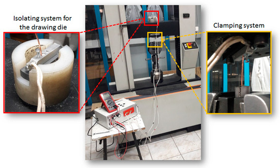
Figure 1.
Electrically assisted wire drawing process schema used in pure copper.
After wire drawing, all specimens were tensile tested by a Zwick/Roell universal tensile machine (model: Z100, ZwickRoell, Gliwice, Poland) with a constant velocity of 0.25 m/min. A load cell (model: Xforce P, ZwickRoelly, Kennesaw, GA, USA) was used with a scale range of 100 kN and an accuracy of 1 N to register the tensile forces. A mechanical extensometer (Zwick, click-on WN:19 extensometer, Kennesaw, GA, USA) was used to measure the material elongation. The material hardness distribution was registered with a durometer (model: Micromet 5114, Buehler, Düsseldorf, Germany). The metallographic structure was observed by a Nikon microscope (model: Optiphot-100, Nikon, Tokyo, Japan) and X-ray diffraction (XRD) analyses were conducted, with a PANalytical X’Pert PRO MPD Alpha1 diffractometer (Malvern Panalytical Ltd., Zürich, Switzerland). A θ–2θ Bragg–Brentano configuration was used with a Cu·Kα1 radiation (λ = 1.5406 and a Ge (111) primary monochromator. A phase analysis of the material was performed with a θ–2θ scan from 40° to 153° with a step size of 0.017° and a measuring time of 150 s per step. Finally, the grain size and twin evolution were analyzed by the electron backscatter diffraction (EBSD) technique, in a Field Emission JEOL JSM 7001-F (JEOL Ltd., Denton, TX, USA) Scanning Electron Microscope (SEM). The voltage was set to 20 kV, with the specimens tilted 70° at a working distance of 10 mm. The step size was 0.03 µm in a square array. Sample preparation included manual grinding up to 6 μm diamond paste, automatic polishing up to 1 μm silica, and final vibratory polishing with 0.05 μm colloidal silica. The software to analyze and evaluate microstructure changes was the toolbox of MTEX [16].
3. Results and Discussion
3.1. Drawing and Tensile Forces
The drawing and tensile tests performed with an Instron 4206 universal testing machine are shown in Figure 2a,b, respectively; the operation parameters are shown in Table 1. It was found that, in comparison to the CD process, the drawing forces decreased by 15–20% and the tensile forces slightly increased, while deformation increased by 20–22% with the application of EPT. The increment on drawing deformation indicated that the ductility of copper wire was improved by drawing with the electropulses. This change in ductility is attributed to micro and meso thermal events at the microstructure defects, promoting a high rise in temperature due to the change of resistivity and, consequently, dislocation movement increase due to this local rise in temperature. When the high-density current pulses with a short duration passed through the deformation area, the metal atoms vibrated due to the rise in temperature, which accelerates the movement of dislocations [10]. The friction between the walls and wire decreases and the yield stress of the wire itself is kept low by heating and hardening reduction; both contributions decrease the necessary drawing force. Egea et al. [14] reported a decrease in drawing forces when the EPT of large pulse duration and lower frequency discharge were applied during the wire drawing process.
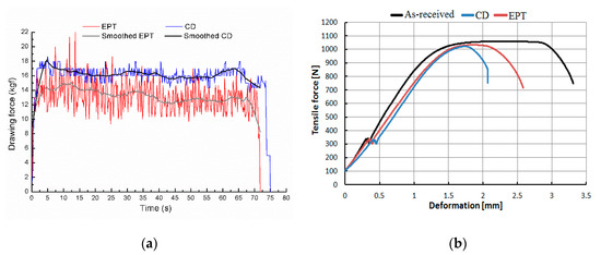
Figure 2.
(a) Drawing forces (kg) as a function of time (s). (b) Tensile forces (N) as a function of drawing deformation (mm). EPT = electropulsing treatment. CD = conventional cold wire drawing process.
The results are in agreement with Zimniak et al. [12], who studied the electroplastic effect in the cold drawing of copper wires. They found that there was a slight increase in tensile strength and a significant increase in the elongation of the tested specimens. The decrease in drawing and tensile forces is due to the rise of temperature caused by joule heating during the EPT process. Consequently, the plastic deformability of copper wire increases and the ultimate tensile strength does not seem to change. Finally, it is important to stress that the EPT specimens presented a better elongation than the CD specimens, but lower than the as-received specimens. Therefore, the annealing treatment is not fulfilled in the EPT with electric configuration used in this work. However, the EPT has provoked an ultra-fast annealing treatment of a few seconds that has improved the material elongation, which is crucial in wire production. This ultra-fast annealing treatment has great potential for the industry due to the time consuming and high cost nature of the conventional annealing process, which requires large furnaces.
3.2. Resistivity and Material Hardness
Table 3 shows the comparison of the electrical resistivity of copper wire drawn by CD and EPT processes. It can be seen that no change in resistivity has been observed during the EPT process. On the contrary, the experimental results [3] have shown that the resistivity of stainless-steel wires with the application of current pulses was decreased by 10% due to retardation in the micro-crack growth rate and reduction in grain boundary cracking [17]. It seems that the rise in temperature, when considering the electroplastic effect in the EPT process of copper wires, makes a small contribution to the changes in the crack initiation and vacancies on the surface of wire. A statistical analysis was carried out to assess whether the CD and EPT values presented significant differences. Accordingly, firstly a Kolmogorov–Smirnov test was completed to denote that the values do not have normal distributions. Consequently, a Wilcoxon–Mann–Whitney test showed a p-value of 0.074, thus there is no statistical difference between both processes and, subsequently, there are no significant differences in the resistivity values. On the other hand, the material hardness of the EPT specimens decreases by 28–33% as compared to the CD specimens, as shown in Figure 3. The hardness and resistivity values were taken with an average of five measurements along the length of the specimen.
Table 3.
Material resistivity for each experimental configuration.
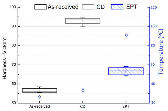
Figure 3.
Material hardness and the bulk temperature recorded during drawing.
In CD, the work hardening occurs due to the increase in cold deformation which decreases the plastic deformability and increases the strength of the material [11]. However, using the EPT process, the annealing process is pretended to be be more economical and plasticity improved. The temperature rise caused by severe plastic deformation when the EPT specimens passed through the drawing die would promote the activation of dislocation annihilation, which decreases the work hardening rate [10]. The decrease in material hardness may be related to the softening effects in the deformation zone due to the influence of the EPT on deformation behavior. The bulk temperature was measured, with a thermocouple type C on the wire surface, right after been deformed by the drawing die. The maximum bulk temperature was about 96 °C for the EPT specimen. However, a larger temperature is expected at the micro scale level on the microstructural features, such as dislocations, grain boundaries, voids due to hot-spot, which can affect the material microstructure.
3.3. Material Microstructure
The Standard Test Methods for Determining Average Grain Size ASTM E112 was used to evaluate the microstructure changes during the wire drawing process. For the EBSD data, the Average Confidence Index and the Mean Angular Deviation for each of the EBSD maps are provided in Table 4. More than 106 steps with a step size of 30 nm and 80% of indexed points were obtained. With the purpose of not disguising any microstructural feature and to take advantage of the high quality of the results, no clean-up subroutines were used. In addition, Figure 4 exhibits the microstructure of the as-received CD and EPT specimens. It is observed that the EPT process had no significant influence on the microstructure. Dynamic recrystallization (DRX) may not have been achieved during the EPT process, as the Joule heating effect was insufficient to reach the DRX temperature of pure copper. It can be assumed that electropulsing could not enhance the mobility of dislocations and voids, which increased the strength of the obstacles opposing the dislocation motion due to the low density of EPT. Retardation of grain growth due to the localized temperature is not high enough to recrystallize grains [17], although it seems to help the activation of multiple slip systems and to reorient some grains.
Table 4.
Number of points indexed, band contrast, and mean angular deviation for each wire drawing configuration.
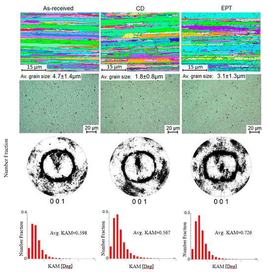
Figure 4.
Microstructure in the longitudinal (first row, electron backscatter diffraction, EBSD) and cross-section views (second row, optical), (001) pole figures (third row) and Kernel Average Misorientation (KAM, fourth row) of the as-received CD and EPT specimens.
Microstructures are shown both in the longitudinal (EBSD) and cross sectional (optic microscopy) views. The longitudinal views exhibit that the as-received material presents more homogeneously elongated grains than CD and EPT, which show fragmented grains or nucleation of smaller subgrains, especially in the EPT specimen. Additionally, the cross-sectional views allow the measurement of transversal grain size averages for each specimen. The average grain sizes are 4.7 ± 1.4 µm, 1.8 ± 0.8 µm, and 3.1 ± 1.3 µm for as-received, CD and EPT, respectively. The reduction of the grain size is attributable to the plastic deformation and there are no apparent differences in the grain sizes of CD and EPT, despite the joule effect experienced by the electropulse-assisted process.
Textures, depicted as (001) pole figures in the third row of Figure 4, show typical fiber texture along the wire longitudinal axes. Some extra orthotropic pole figure symmetry may come from the action of the wire drawing tools and consequent surface shearing. Furthermore, in the fourth row, Kernel Average Misorientations (KAM) distributions and average KAM show that defect accumulation is larger in the EPT sample than in CD sample. What seems somehow contradictory, which can be associated to a more heterogeneous deformation field on the larger spread, evident on the (001) pole figure. Heating might stabilize high angle grain boundaries (HAGB), due to the dissolution and migration of low angle dislocation arrays that cannot be easily detected by the EBSD technique.
For further analysis of the grain boundaries, Figure 5 shows the length fraction (LF) of grain boundaries at different misorientation angles. It is observed that at smaller angles, the LF for CD samples is lower than for the EPT specimens. However, as the misorientation angle increases, the LF decreases for the EPT samples. Dislocations create arrays of high angle boundaries (HAB) during CD. Although during the EPT the low angle grain boundaries (LAGB) tend to be stabilized, due to the continuous recrystallization caused by a localized heating [18]. There is no evidence of twining detected, either by Coincident Site Lattice (CSL) or by any other misorientation characteristic Grain average misorientations (GAM) were also calculated and they are in fair agreement with the Kernel Average Misorientations (KAM) shown in Figure 4. The distributions are fairly lognormal with average values shown in Table 5. The presented values are different from the ones shown for the particular scans in Figure 4, but the general behavior is similar. Unexpected diminishment in the CD sample, for all methods (KAM, GAM, HAGB, LAGB) that evaluate defect storage, suggests that continuous dynamic recrystallization (CDR), somehow cleans up some defects without any extra external heating and is only driven by the same deformation and temperature of the samples. It is expected that these microstructure changes reflect local heat treatments influencing the development of residual stresses in the wire, which is crucial for the number of drawing steps before annealing treatment.
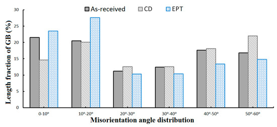
Figure 5.
Overall distribution of low and high angle grain boundaries.
Table 5.
Kernel average misorientation and grain average misorientation.
3.4. Residual Stresses
The tensile residual stresses developed due to inhomogeneous deformation cause splitting at the surface of wire during the drawing process [19]. The use of EPT decreased the residual stresses and they decreased further with the increase in current density [20]. The residual stresses were recorded in the as-received and after wire drawing states in CD and EPT processes to describe the stresses from the surface through the in-depth direction. Figure 6 shows the results of residual stresses in the in-depth direction for the three configurations. The average values are the average of four measurements by the Sin2φ method. The error bars show the standard deviation of these measurements.
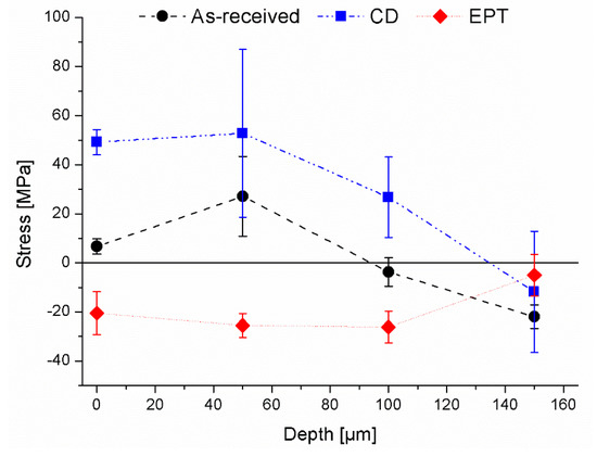
Figure 6.
Residual stress variations from the surface to the in-depth direction of the B, CD and EPT wire drawn specimens.
The as-received material shows tensile residual stresses of about 5 MPa at the surface and compressive residual stresses of −15 MPa at 150 µm deep to the center of the wire. Looking at the results of the CD specimen, similar trends but higher values of stresses were found. However, the EPT specimens exhibit a different trend with respect to the other two configurations. In particular, these residual stresses are under a compression of about −20 MPa at the surface and −5 MPa at the 150 µm in-depth position. These thermal compressive stresses can be explained through rapid local thermal expansion by applying EPT during the drawing of copper wires. It was found that an electric current with appropriate current density is necessary to reduce the crack growth rate and enhance the fatigue life of ductile material copper [21]. Therefore, EPT can be considered a potential effective method for improving the plastic deformability of copper wires, by reducing the drawing forces and inducing compressive residual stresses. This compressive stresses enhance the wire strength for the forthcoming drawing steps but the material’s resistivity is not compromised.
4. Conclusions
The present work analyzed the wire drawing process of pure copper with simultaneous EPT, with the aim of avoiding annealing thermal treatments. From the results, the following conclusions can be summarized:
- Lower drawing forces and higher ductility properties were found in the pure copper specimens drawn by electropulsing compared with conventionally drawn specimens. Accordingly, the EPT improves the plasticity and increases the strength of copper wires by reducing the annealing treatment to make the process more economical.
- The EPT did not change the material resistivity of the wires with respect to the as-received specimens. On the contrary, the plastic deformation, without any type of thermal treatment (CD), was shown to increase the conductivity by about 4%, which might be related to the CDR effect during processing.
- The material microstructure exhibited similar average grain sizes and different low and grain boundaries for CD and EPT. Therefore, the thermal contribution due to the electropulsing is not sufficient to change the grain size, although changes in the grain boundaries and dislocation arrays that affect the residual stresses were observed.
- Compressive residual stresses of about −20 MPa were found along the in-depth direction in the EPT specimens. Consequently, these compressive stresses prevent the fatigue cracking at the surface of the wires for the future wire drawing steps.
Author Contributions
Conceptualization, H.A.G.R. and A.J.S.E.; data curation, S.H. and R.B.; funding acquisition, A.J.S.E.; methodology, H.A.G.R. and A.J.S.E.; validation, S.H. and R.B.; writing original draft, S.H. and A.J.S.E.; writing, review, and editing, H.A.G.R. and R.B.
Funding
This work is supported by the National Council for Scientific and Technological Development of Chile (Fondecyt projects 3180006), the Serra Húnter program (Generalitat de Catalunya) reference number UPC-LE-304.
Acknowledgments
Thanks to Prysmian Group S.A. for providing the raw material and the drawing tools for the drawing experiments.
Conflicts of Interest
The authors declare no conflict of interest.
References
- Da Silva Bernardo, R.; Fernandes Neto, M. Influence of a cold deformation process by drawing on the electrical properties of copper wires. REM-Int. Eng. J. 2017, 70, 53–57. [Google Scholar] [CrossRef][Green Version]
- Akbari, A.; Hasani, G.H.; Jam, M.J. An Experimental Investigation on the Effect of Annealing Treatment on Strain Inhomogeneity in the Cross-Section of Drawn Copper Wires; EU: Roznov pod Radhostem, Czech Republic, 2010. [Google Scholar]
- Tang, G.; Zhang, J.; Zheng, M.; Zhang, J.; Fang, W.; Li, Q. Experimental study of electroplastic effect on stainless steel wire 304L. Mater. Sci. Eng. A 2000, 281, 263–267. [Google Scholar] [CrossRef]
- Sergey, K.; Mei, S.; Kirill, O.; Roman, F.; Irina, K. Change in plasticity of copper under weak electrical potentials. In IOP Conference Series: Materials Science and Engineering; IOP Publishing: Bristol, UK, 2019. [Google Scholar]
- Vega, G.; Haddi, A.; Imad, A. Investigation of process parameters effect on the copper-wire drawing. Mater. Des. 2009, 30, 3308–3312. [Google Scholar] [CrossRef]
- Tang, G.; Zhang, J.; Yan, Y.; Zhou, H.; Fang, W. The engineering application of the electroplastic effect in the cold-drawing of stainless steel wire. J. Mater. Process. Technol. 2003, 137, 96–99. [Google Scholar] [CrossRef]
- Zhang, D.; To, S.; Zhu, Y.H.; Wang, H.; Tang, G.Y. Static electropulsing-induced microstructural changes and their effect on the ultra-precision machining of cold-rolled AZ91 alloy. Metall. Mater. Trans. 2011, 43, 1341–1346. [Google Scholar] [CrossRef]
- Tadic, N.; Jelic, M.; Lucic, D.; Misovic, M. Relaxation of the residual stresses produced by plastic deformation. Mater. Technol. 2011, 45, 467–475. [Google Scholar]
- Ripoll, M.R.; Weygand, S.M.; Riedel, H. Reduction of tensile residual stresses during the drawing process of tungsten wires. Mater. Sci. Eng. A 2010, 527, 3064–3072. [Google Scholar] [CrossRef]
- Yao, K.-F.; Wang, J.; Zheng, M.; Yu, P.; Zhang, H. A research on electroplastic effects in wire-drawing process of an austenitic stainless steel. Scr. Mater. 2001, 45, 533–539. [Google Scholar] [CrossRef]
- Tang, G.; Zheng, M.; Zhu, Y.; Zhang, J.; Fang, W.; Li, Q. The application of the electro-plastic technique in the cold-drawing of steel wires. J. Mater. Process. Technol. 1998, 84, 268–270. [Google Scholar] [CrossRef]
- Zimniak, Z.; Radkiewicz, G. The electroplastic effect in the cold-drawing of copper wires for the automotive industry. Arch. Civ. Mech. Eng. 2008, 8, 173–179. [Google Scholar] [CrossRef]
- Troitskiy, O.A.; Stashenko, V.I. Electroplastic Wire Drawing: A Promising Method of Production of Lightweight Wire and Cable. J. Mach. Manuf. Reliab. 2015, 44, 758–765. [Google Scholar] [CrossRef]
- Egea, A.J.S.; Rojas, H.A.G.; Celentano, D.J.; Peiró, J.J. Mechanical and metallurgical changes on 308L wires drawn by electropulses. Mater. Des. 2016, 90, 1159–1169. [Google Scholar] [CrossRef]
- Egea, A.J.S.; Peiró, J.J.; Signorelli, J.W.; Rojas, H.A.G.; Celentano, D.J. On the microstructure effects when using electropulsing versus furnace treatments while drawing Inox 308L. J. Mater. Res. Technol. 2019, 8, 2269–2279. [Google Scholar] [CrossRef]
- Hielscher, R.; Schaeben, H. A novel pole figure inversion method: Specification of the MTEX algorithm. J. Appl. Cryst. 2008, 41, 1024–1037. [Google Scholar] [CrossRef]
- Wang, X.; Egea, A.J.S.; Xu, J.; Meng, X.; Wang, Z.; Shan, D.; Guo, B.; Cao, J. Current-Induced Ductility Enhancement of a Magnesium Alloy AZ31 in Uniaxial Micro-Tension Below 373 K. Materials 2019, 12, 111. [Google Scholar] [CrossRef] [PubMed]
- Xu, Q.; Tang, G.; Jiang, Y.; Hu, G.; Zhu, Y. Accumulation and annihilation effects of electropulsing on dynamic recrystallization in magnesium alloy. Mater. Sci. Eng. A 2011, 528, 3249–3252. [Google Scholar] [CrossRef]
- Sharpe, W.N. Experimental Solid Mechanics; Springer: Boston, MA, USA, 2008; pp. 371–386. [Google Scholar]
- Long, P. Influence of electropulsing treatment on residual stresses and tensile strength of as-quenched medium carbon steel. J. Phys. Conf. Ser. 2019, 1187, 032054. [Google Scholar] [CrossRef]
- Yin, Y.; Chen, H.; Morita, Y.; Toku, Y.; Ju, Y. Effect of electropulsing treatment on the fatigue crack growth behavior of copper. Materials 2018, 11, 2168. [Google Scholar] [CrossRef] [PubMed]
© 2019 by the authors. Licensee MDPI, Basel, Switzerland. This article is an open access article distributed under the terms and conditions of the Creative Commons Attribution (CC BY) license (http://creativecommons.org/licenses/by/4.0/).