Crystal Structures of GaN Nanodots by Nitrogen Plasma Treatment on Ga Metal Droplets


Abstract
1. Introduction
2. Materials and Methods
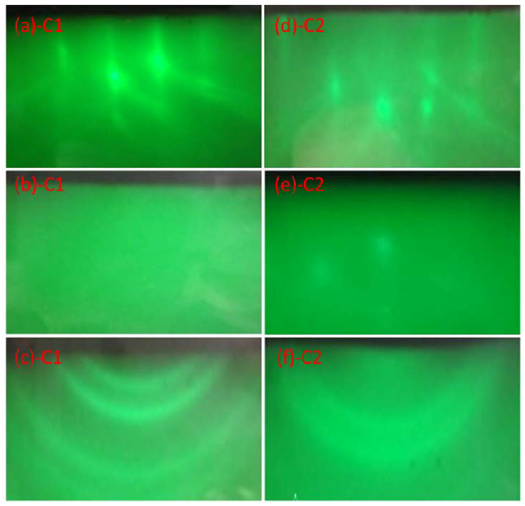
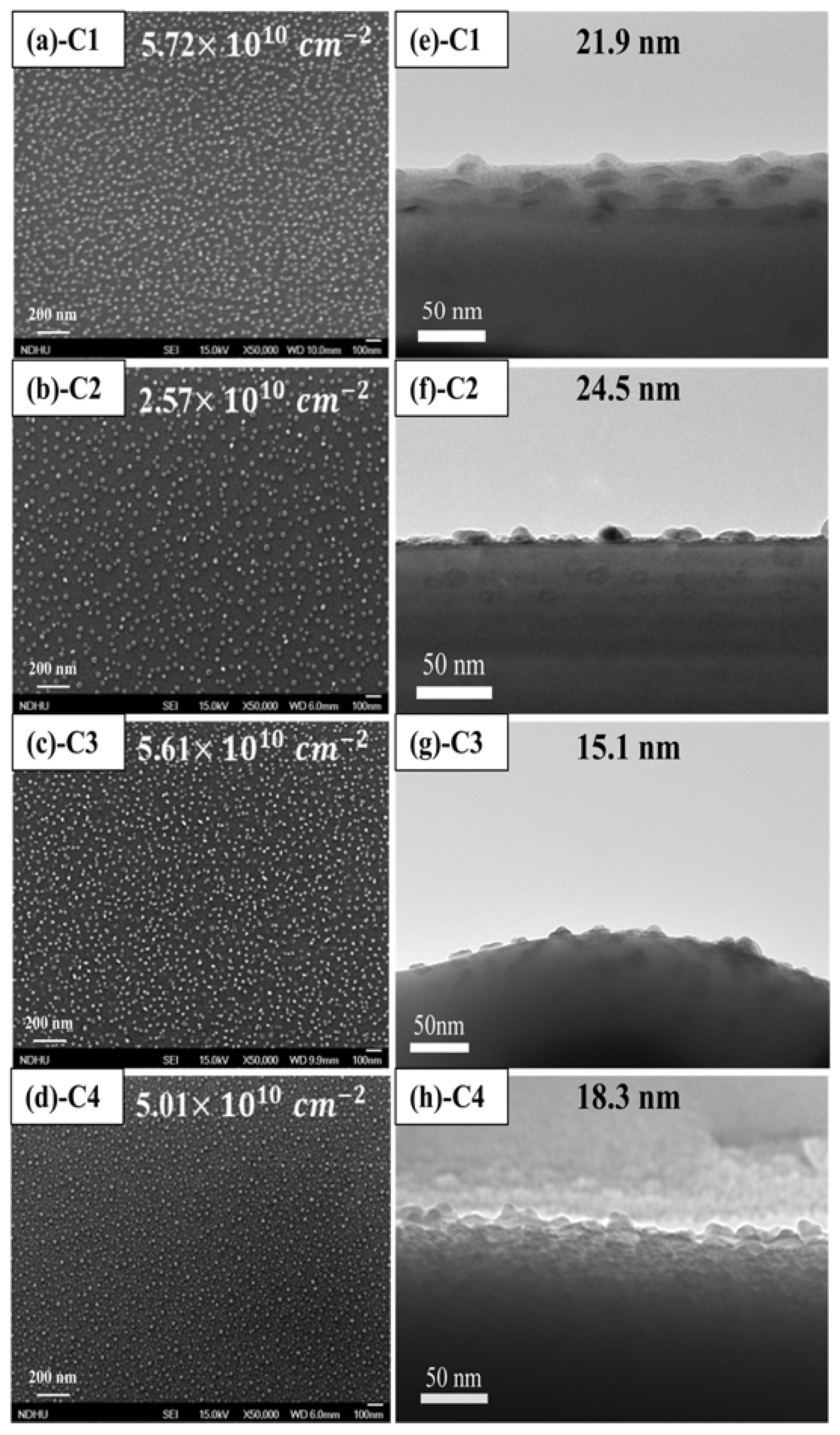
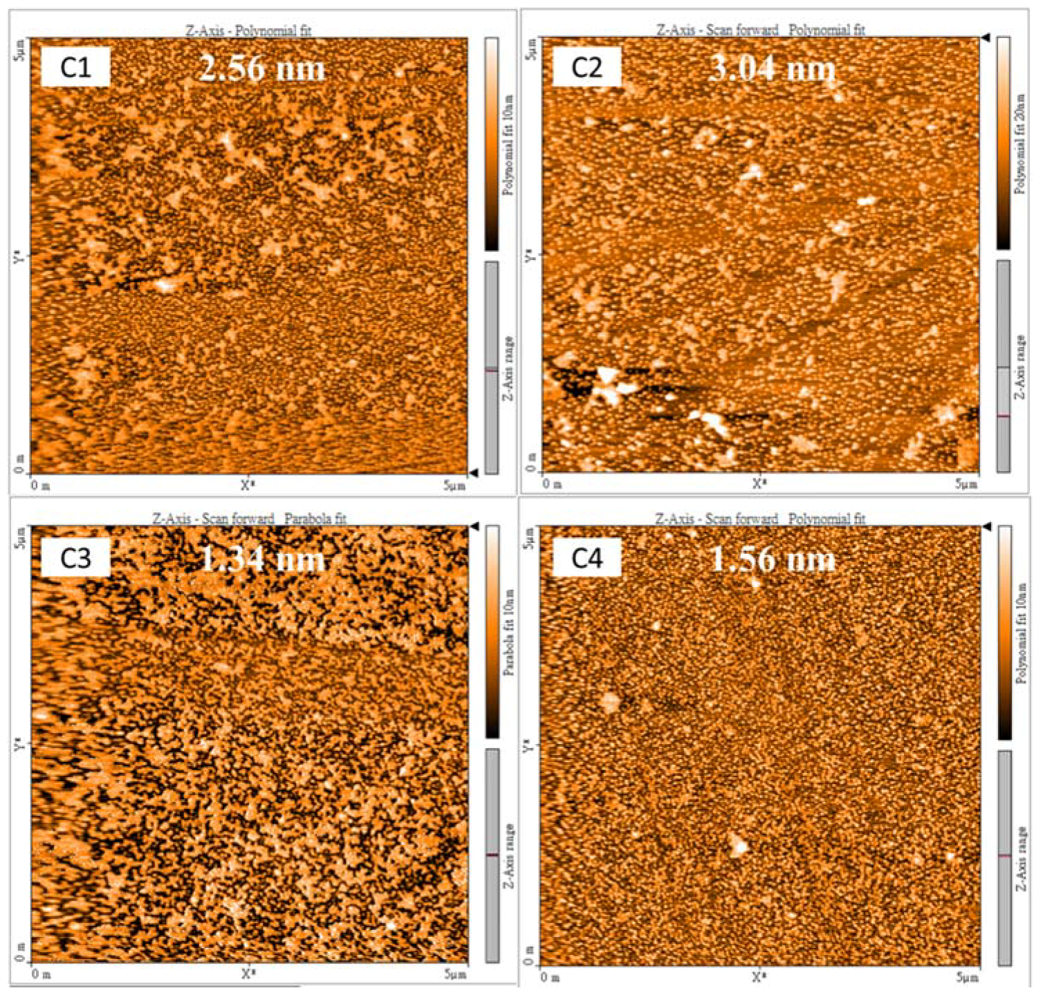
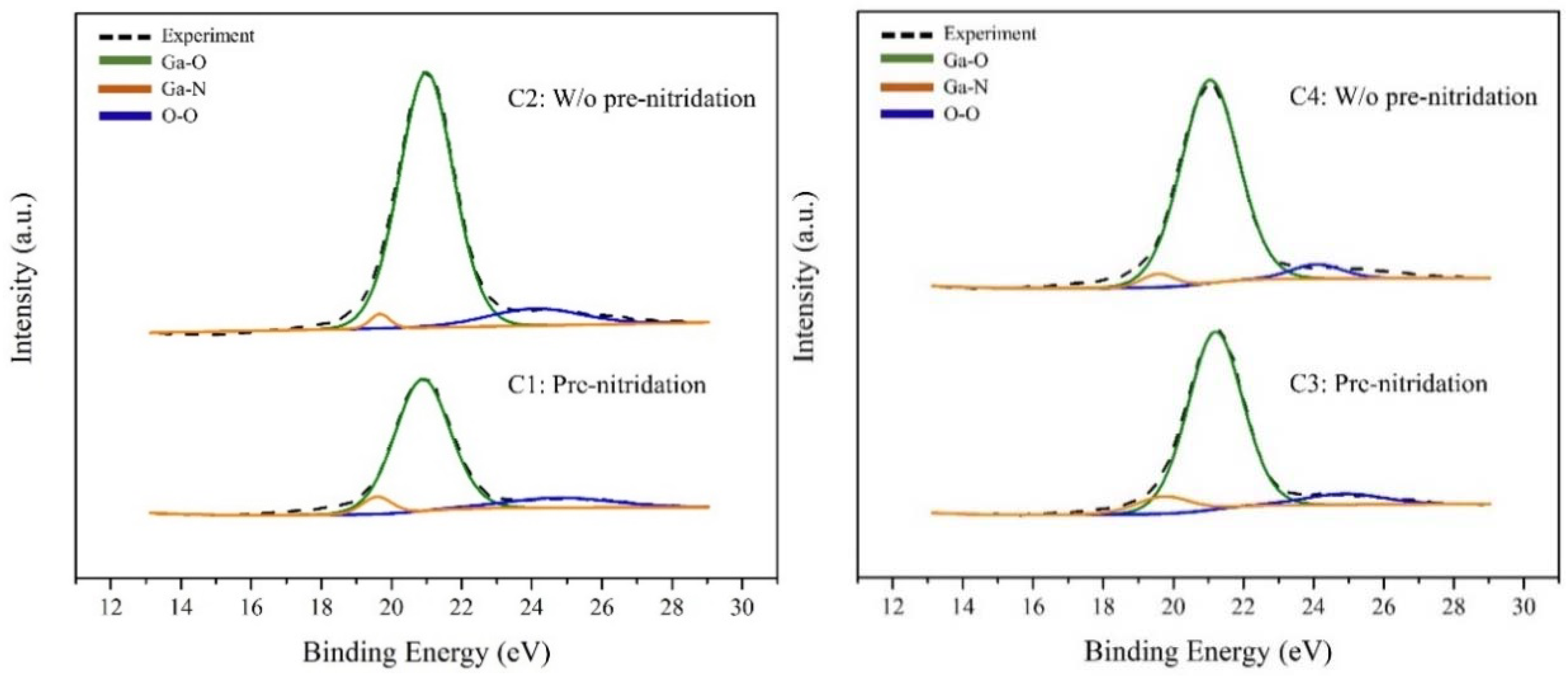
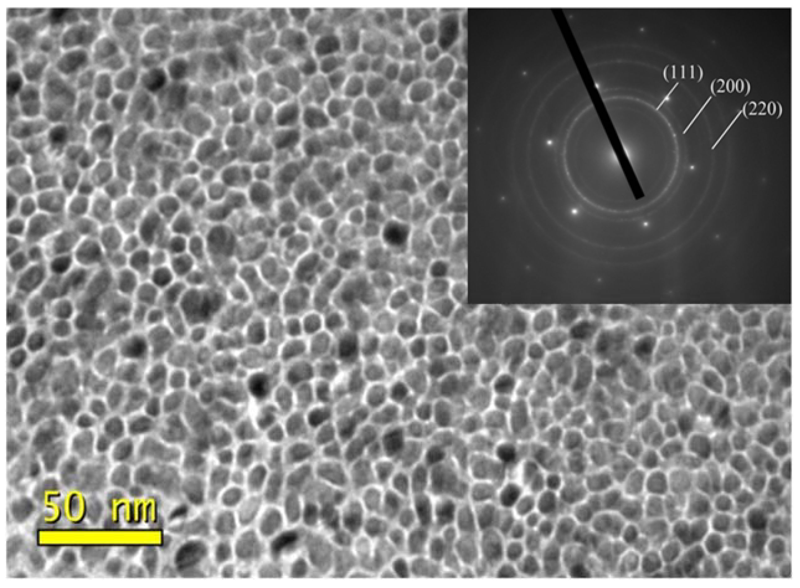
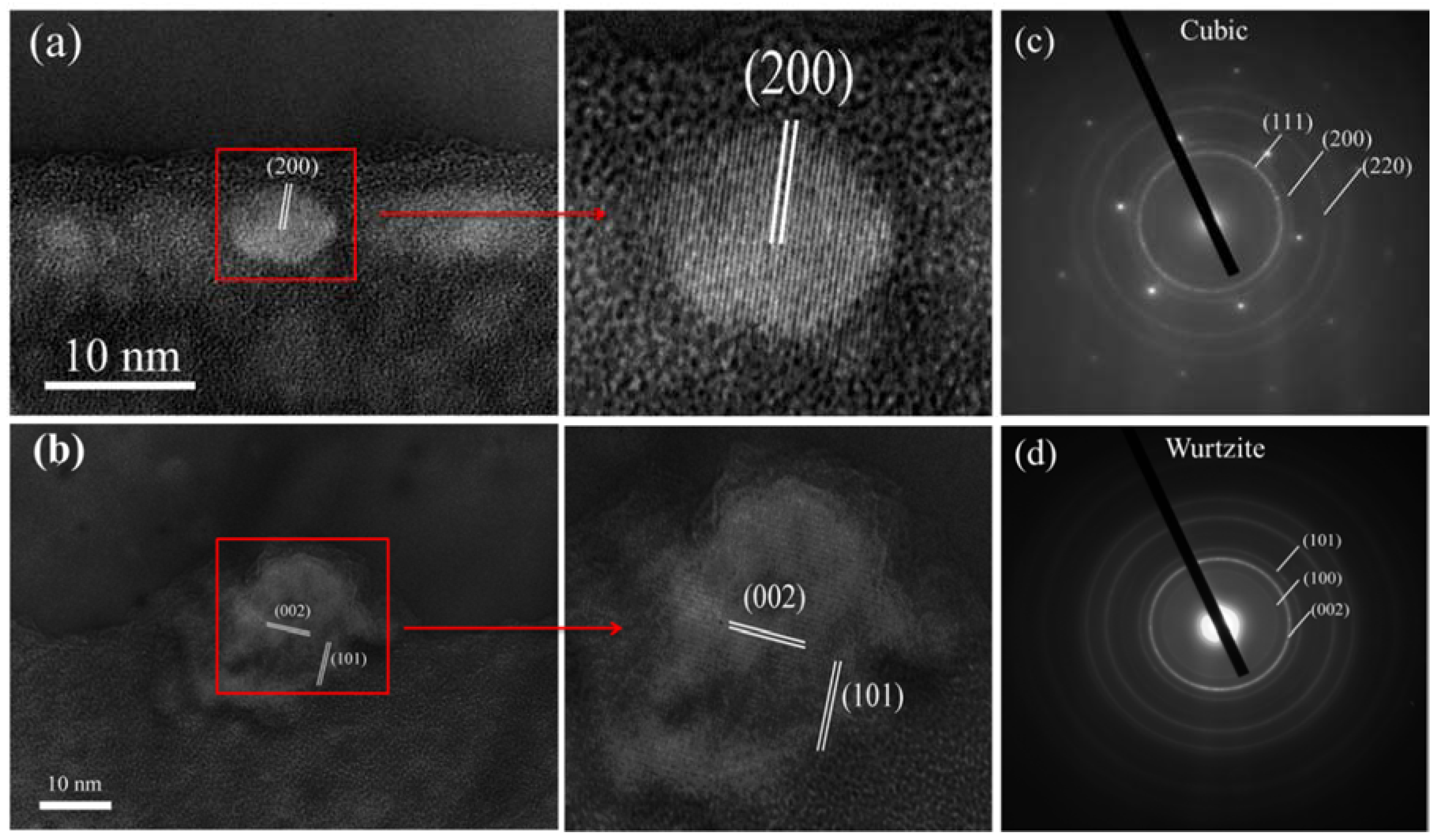
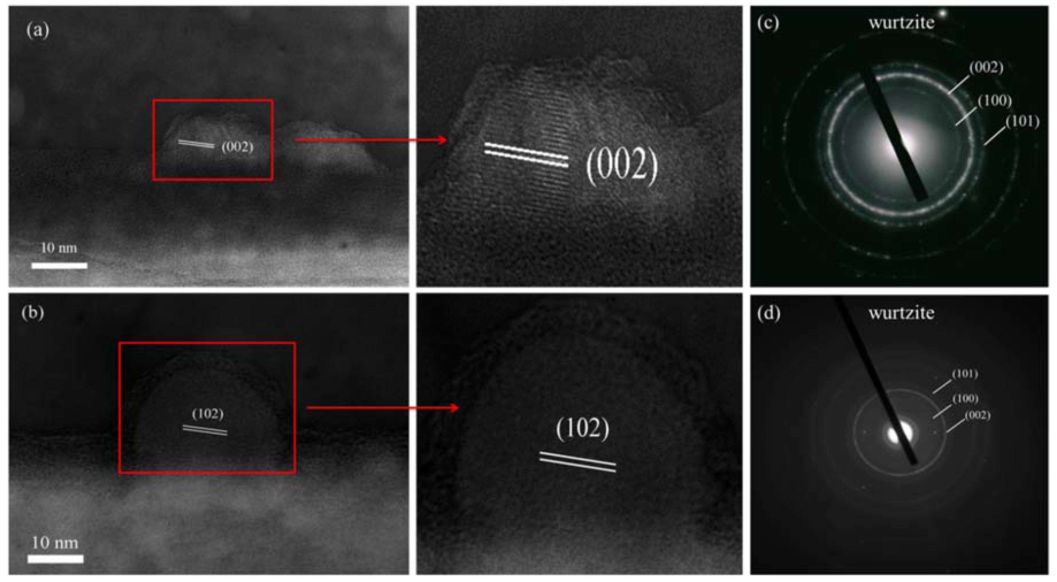
3. Results and Discussion
4. Conclusions
Author Contributions
Funding
Acknowledgments
Conflicts of Interest
References
- Wu, J. When group-III nitrides go infrared: New properties and perspectives. J. Appl. Phys. 2009, 106, 011101. [Google Scholar] [CrossRef]
- Nakamura, S.; Pearton, S.; Fasol, G. The Blue Laser Diode, 2nd ed.; Springer: Berlin, Germany, 2000. [Google Scholar]
- Su, M.; Chen, C.; Rajan, S. Prospects for the application of GaN power devices in hybrid electric vehicle drive systems. Semicond. Sci. Technol. 2013, 28, 074012. [Google Scholar] [CrossRef]
- Kako, S.; Holmes, M.; Sergent, S.; Burger, M.; As, D.J.; Arakawa, Y. Single-photon emission from cubic GaN quantum dots. Appl. Phys. Lett. 2014, 104, 011101. [Google Scholar] [CrossRef]
- Chou, H.T.; Goldhaber-Gordon, D.; Schmult, S.; Manfra, M.J.; Sergent, A.M.; Molnar, R.J. Single-electron transistors in GaN/AlGaN heterostructures. Appl. Phys. Lett. 2006, 89, 033104. [Google Scholar] [CrossRef]
- D’Amico, I.; Biolatti, E.; Rossi, F.; Derinaldis, S.; Rinaldis, R.; Cingolani, R. GaN quantum dot based quantum information/computing processing. Superlattices Microstruct. 2002, 31, 117–125. [Google Scholar] [CrossRef]
- Novikov, S.V.; Kent, A.J.; Foxon, C.T. Molecular beam epitaxy as a growth technique fpr achieving free-standing zinc-blende GaN and wurtzite AlxGa1−xN. Prog. Cryst. Growth Charact. Mater. 2017, 63, 25–39. [Google Scholar] [CrossRef]
- Susanto, I.; Kan, K.Y.; Yu, I.S. Temperature effects for GaN films grown on 4H-SiC substrate with 40 miscutting orientation by plasma-assisted molecular beam epitaxy. J. Alloys Compd. 2017, 723, 21–29. [Google Scholar] [CrossRef]
- Nakamura, S. GaN growth using GaN buffer layer. Jpn. J. Appl. Phys. 1991, 30, L1705–L1707. [Google Scholar] [CrossRef]
- Sudhir, G.S.; Fujii, H.; Wong, W.S.; Kisielowski, C.; Newman, N.; Dieker, C.; Liliental-Weber, Z.; Rubin, M.D.; Weber, E.R. Pulsed laser deposition of aluminum nitride and gallium nitride thin films. Appl. Surf. Sci. 1998, 127–129, 471–476. [Google Scholar] [CrossRef]
- Paskova, T.; Darakchieva, V.; Valcheva, E.; Paskov, P.P.; Ivanov, I.G.; Monemar, B.; Böttcher, T.; Roder, C.; Hommel, D. Hydride vapor-phase epitaxial GaN thick films for quasi-substrate applications: Strain distribution and wafer bending. J. Electron. Mater. 2004, 33, 389–394. [Google Scholar] [CrossRef]
- Brown, J.; Wu, F.; Petroff, P.M.; Speck, J.S. GaN quantum dot density control by rf-plasma molecular beam epitaxy. Appl. Phys. Lett. 2004, 84, 690–692. [Google Scholar] [CrossRef]
- Carlsson, N.; Seifert, W.; Petersson, A.; Castrillo, P.; Pistol, M.E.; Samuelson, L. Study of the two-dimensional–three-dimensional growth mode transition in metal-organic vapor phase epitaxy of GaInP/InP quantum-sized structures. Appl. Phys. Lett. 1994, 65, 3039. [Google Scholar] [CrossRef]
- Koguchi, N.; Tasahashi, S.; Chikyow, T. New MBE method for InSb quantum well boxes. J. Cryst. Growth 1991, 111, 688–692. [Google Scholar] [CrossRef]
- Wang, Z.M.; Holmes, K.; Mazur, Y.I.; Ramsey, K.A.; Salamo, G.J. Self-organization of quantum-dot pairs by high-temperature droplet epitaxy. Nanoscale Res. Lett. 2006, 1, 57–61. [Google Scholar] [CrossRef]
- Wu, C.L.; Chou, L.J.; Gwo, S. Size- and shape-controlled GaN nanocrystals grown of Si(111) substrate by reactive epitaxy. Appl. Phys. Lett. 2004, 85, 2071–2073. [Google Scholar] [CrossRef]
- Kondo, T.; Saitoh, K.; Yamamoto, Y.; Maruyama, T.; Naritsuka, S. Fabrication of GaN dot structures on Si substrates by droplet epitaxy. Phys. Stat. Sol. A 2006, 1700–1703. [Google Scholar] [CrossRef]
- Wang, Y.; Ozcan, A.S.; Sanborn, C.; Ludwig, K.F.; Bhattacharyya, A.; Chandrasekran, R.; Moustakas, T.D.; Zhou, L.; Smith, D.J. Real-time X-ray studies of gallium nitride nanodot formation by droplet heteroepitaxy. J. Appl. Phys. 2007, 102, 073522. [Google Scholar] [CrossRef]
- Yu, I.S.; Chang, C.P.; Yang, C.P.; Lin, C.T.; Ma, Y.R.; Chen, C.C. Characterization and density control of GaN nanodots on Si (111) by droplet epitaxy using plasma-assisted molecular beam epitaxy. Nanoscale Res. Lett. 2014, 9, 682. [Google Scholar] [CrossRef]
- Miller, D.A.B.; Chemla, D.S.; Damen, T.C.; Gossard, A.C.; Wiegmann, M.; Wood, T.H.; Burrus, C.A. Band-edge electroabsorption in quantum well structures: The quantum-confined stark effect. Phys. Rev. Lett. 1984, 53, 2173. [Google Scholar] [CrossRef]
- Naritsuka, S.; Kondo, T.; Otsubo, H.; Saitoh, K.; Yamamoto, Y.; Maruyama, T. In situ annealing of GaN dot structures grown by droplet epitaxy on (111) Si substrates. J. Cryst. Growth 2007, 300, 118–122. [Google Scholar] [CrossRef]
- Qin, H.; Luan, X.; Feng, C.; Yang, D.; Zhang, G. Mechanical, thermodynamic and electronic properties of wurtzite and zinc-blende GaN crystals. Materials 2017, 10, 1419. [Google Scholar] [CrossRef]
- Simon, J.; Pelekanos, N.T.; Adelmann, C.; Martinez-Guerrero, E.; André, R.; Daudin, B.; Dang, L.S.; Mariette, H. Direct comparison of recombination dynamics in cubic and hexagonal GaN/AlN quantum dots. Phys. Rev. B 2003, 68, 035312. [Google Scholar] [CrossRef]
- Martinez-Guerrero, E.; Chabuel, F.; Daudin, B.; Rouviere, J.L.; Mariette, H. Control of the morphology transition for the growth of cubic GaN/AlN nanostructures. Appl. Phys. Lett. 2002, 81, 5117. [Google Scholar] [CrossRef]
- Gogneau, N.; Jalabert, D.; Monroy, E.; Shibata, T.; Tanaka, M.; Daudin, B. Structure of GaN quantum dots grown under modified Stranski-Krastanow conditions on AlN. J. Appl. Phys. 2003, 94, 2254–2261. [Google Scholar] [CrossRef]
- Niu, L.; Hao, Z.; Hu, J.; Hu, Y.; Wang, L.; Luo, Y. Improving the emission efficiency of MBE-grown GaN/AlN QDs by strain control. Nanoscale Res. Lett. 2011, 6, 611. [Google Scholar] [CrossRef]
- Schupp, T.; Meisch, T.; Neuschl, B.; Feneberg, M.; Thonke, K.; Lischka, K.; As, D.J. Droplet epitaxy of zinc-blende GaN quantum dots. J. Cryst. Growth 2010, 312, 3235–3237. [Google Scholar] [CrossRef]
- Kawaharazuka, A.; Yoshizaki, T.; Hiratsuka, T.; Horikoshi, Y. Effect of surface Ga accumulation on the growth of GaN by molecular beam epitaxy. Phys. Status Solidi C 2010, 7, 342–346. [Google Scholar] [CrossRef]
- Copel, M.; Reuter, M.C.; Kaxiras, E.; Tromp, R.M. Surfactants in epitaxial growth. Phys. Rev. Lett. 1989, 63, 632–635. [Google Scholar] [CrossRef]
- Andrieu, S.; Frechard, P. What information can be obtained by RHEED applied on polycrystalline films? Surf. Sci. 1996, 360, 289–296. [Google Scholar] [CrossRef]
- Wang, K.; Singh, J.; Pavlidis, D. Theoretical study of GaN growth: A Monte Carlo approach. J. Appl. Phys. 1994, 76, 3502–3510. [Google Scholar] [CrossRef]
- Lymperakis, L.; Neugebauer, J. Large anisotropic adatom kinetics on nonpolar GaN surfaces: Consequences for surface morphologies and nanowire growth. Phys. Rev. B 2009, 79, 241308. [Google Scholar] [CrossRef]
- Monu, M.; Krishna, T.C.S.; Neha, A.; Mandeep, K.; Sandeep, S.; Govind, G. Pit assisted oxygen chemisorptions on GaN surface. Phys. Chem. Chem. Phys. 2015, 17, 15201–15208. [Google Scholar] [CrossRef]
- Chen, H.J.Y.; Su, Y.Z.; Yang, D.L.; Huang, T.W.; Yu, I.S. Effects of substrate pre-nitridation and post-nitridation processes on InN quantum dots with crystallinity by droplet epitaxy. Surf. Coat. Technol. 2017, 324, 491–497. [Google Scholar] [CrossRef]
- CrystOrient. Available online: http://www.crystorient.com/ (accessed on 3 April 2018).
- Romano, L.T.; Krusor, B.S.; Singh, R.; Moustakas, T.D. Structure of GaN films grown by molecular beam epitaxy on (0001) sapphire. J. Electron. Mater. 1997, 26, 285–289. [Google Scholar] [CrossRef]


| Sample | C1 | C2 | C3 | C4 |
|---|---|---|---|---|
| Pre-nitridation | Yes | No | Yes | No |
| Substrate temperature | 500 °C | 500 °C | 550 °C | 550 °C |
| Nitridation time | 5 min | 5 min | 10 min | 10 min |
© 2018 by the authors. Licensee MDPI, Basel, Switzerland. This article is an open access article distributed under the terms and conditions of the Creative Commons Attribution (CC BY) license (http://creativecommons.org/licenses/by/4.0/).
Share and Cite
Su, Y.-Z.; Yu, I.-S. Crystal Structures of GaN Nanodots by Nitrogen Plasma Treatment on Ga Metal Droplets. Metals 2018, 8, 419. https://doi.org/10.3390/met8060419
Su Y-Z, Yu I-S. Crystal Structures of GaN Nanodots by Nitrogen Plasma Treatment on Ga Metal Droplets. Metals. 2018; 8(6):419. https://doi.org/10.3390/met8060419
Chicago/Turabian StyleSu, Yang-Zhe, and Ing-Song Yu. 2018. "Crystal Structures of GaN Nanodots by Nitrogen Plasma Treatment on Ga Metal Droplets" Metals 8, no. 6: 419. https://doi.org/10.3390/met8060419
APA StyleSu, Y.-Z., & Yu, I.-S. (2018). Crystal Structures of GaN Nanodots by Nitrogen Plasma Treatment on Ga Metal Droplets. Metals, 8(6), 419. https://doi.org/10.3390/met8060419