Behavior of Waste Printed Circuit Board (WPCB) Materials in the Copper Matte Smelting Process


Abstract
1. Introduction
2. Materials and Methods
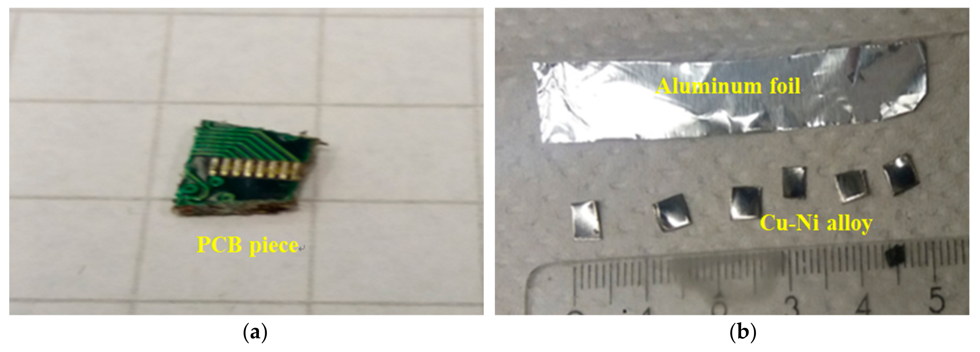
2.1. Materials
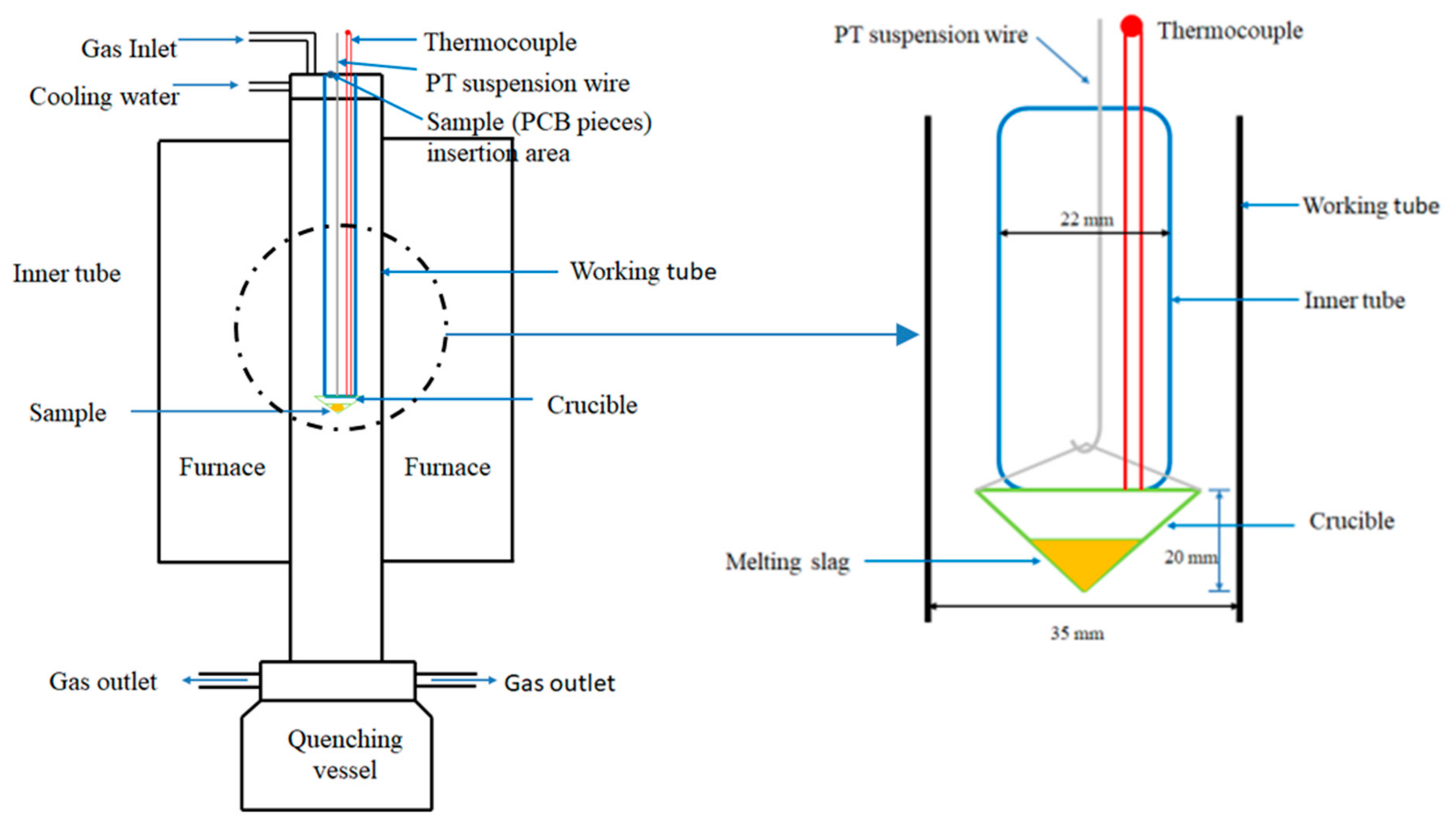
2.2. Apparatus
2.3. Procedure
3. Results and Discussion
3.1. Basic Matte–Slag Reaction during the Flash-Smelting Process
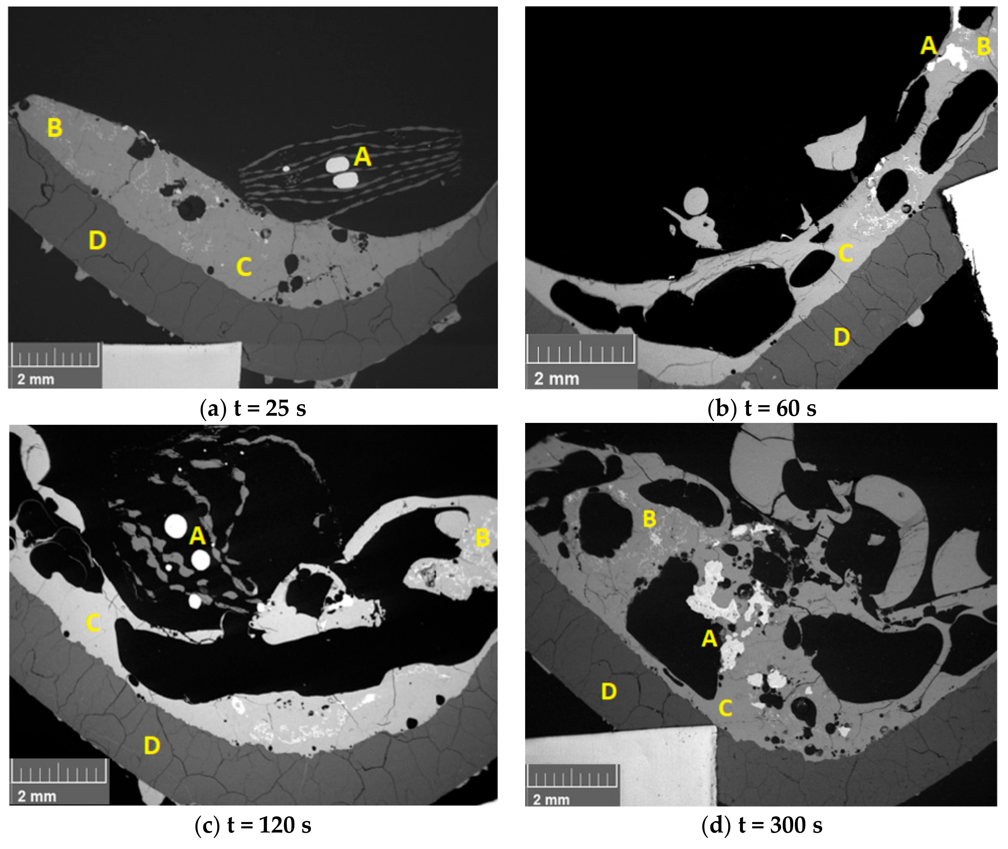
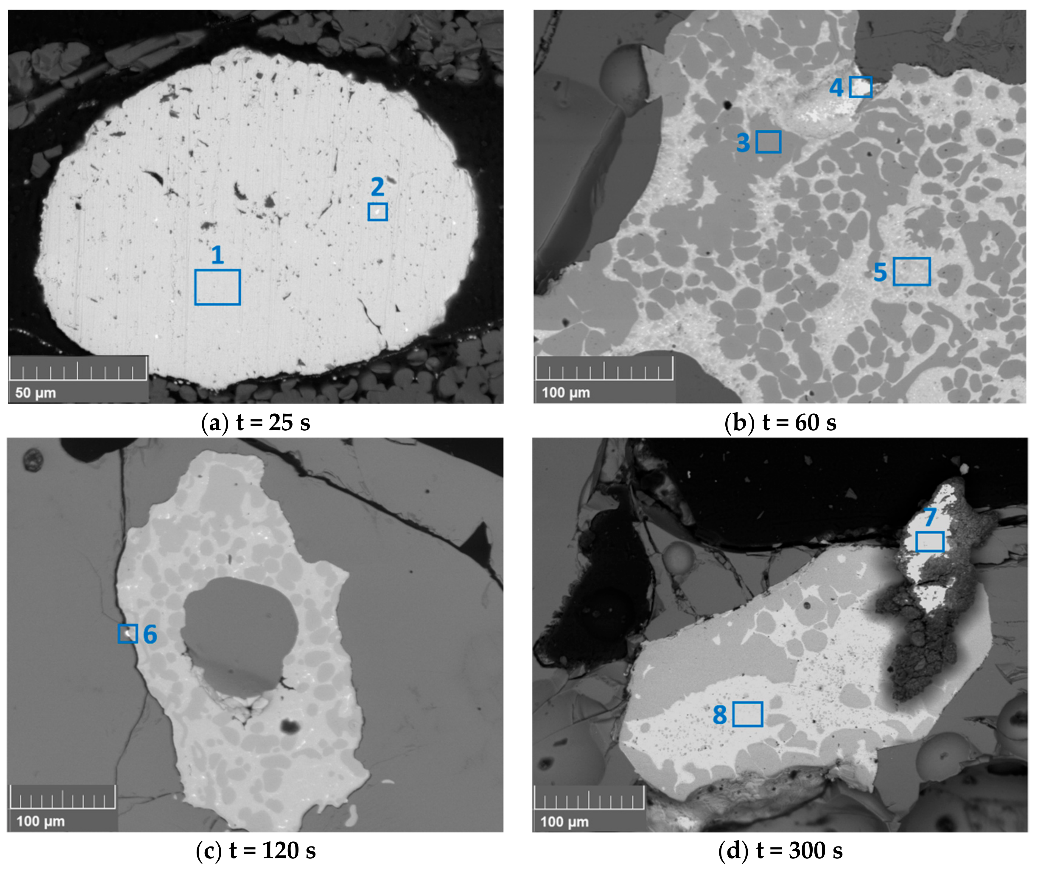
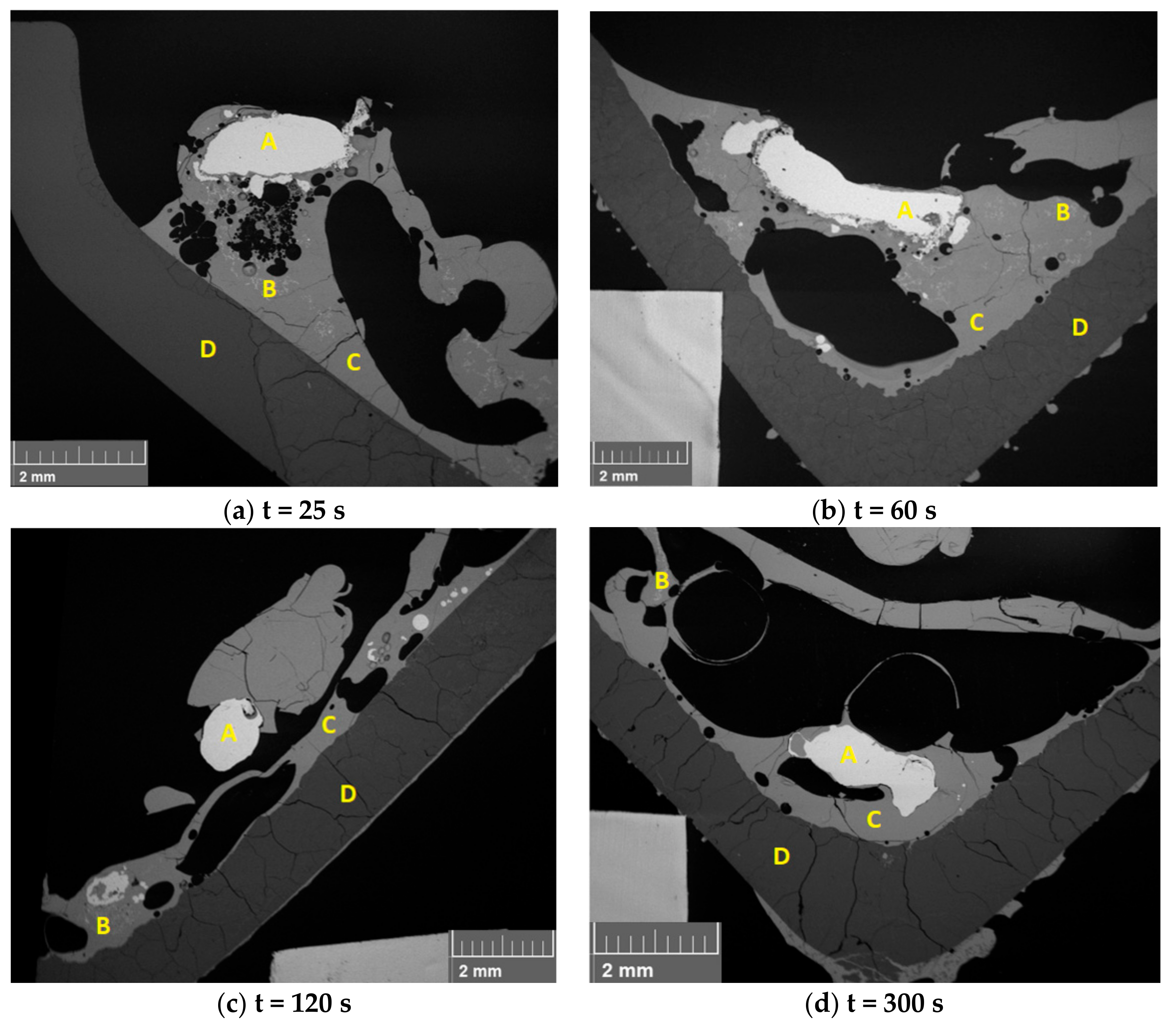
3.2. Behavior of WPCB Samples in the Slag Phase
3.3. Behavior of Synthetic PCB Samples in the Slag Phase
4. Conclusions
- (1)
- In this research, 5 min was enough for the samples to completely melt, but the settling process needs more time. In industrial flash-smelting operations, the amount of WPCB scrap feed is much higher and the required melting time needs further investigation and simulation.
- (2)
- WPCB materials can be added into the FS process, and the metal fraction melts readily and forms droplets that settle through the slag layer and mix into the matte phase. However, the ceramic and plastic fractions of WPCB should be removed before; especially the plastic fraction that may cause both production and safety problems. The possible pyrolysis or combustion behavior in the concentrate suspension and slag reduction in the settler also require thorough investigation before larger quantities of WPCB can be safely used as raw material in an industrial-scale process. If not removed in a pretreatment process, the pyrolysis products of the plastic fraction would change the composition of the flue gas, and the recovery and use of flue gas for sulfuric acid production would be influenced by these organic impurities.
- (3)
- The ceramic fraction of the WPCB dissolves into the slag phase after melting, so the slag volume increases if WPCB materials are added in larger amounts.
- (4)
- The precious metals (for example Au, Ag, and Pt) in the WPCB enter the matte phase in the industrial FS process after settling, and they are finally recovered from the anode slime.
Author Contributions
Funding
Conflicts of Interest
References
- Radulovic, V. Portrayals in Print: Media Depictions of the Informal Sector’s Involvement in Managing E-Waste in India. Sustainability 2018, 10, 966. [Google Scholar] [CrossRef]
- Baldé, C.P.; Forti, V.; Gray, V.; Kuehr, R.; Stegmann, P. The Global E-Waste Monitor 2017: Quantities, Flows and Resources; United Nations University: Bonn, Germany; International Telecommunication Union: Geneva, Switzerland; International Solid Waste Association: Vienna, Austria, 2017. [Google Scholar]
- Ghosh, B.; Ghosh, M.K.; Parhi, P.; Mukherjee, P.S.; Mishra, B.K. Waste Printed Circuit Boards recycling: An extensive assessment of current status. J. Clean. Prod. 2015, 94, 5–19. [Google Scholar] [CrossRef]
- Khaliq, A.; Rhamdhani, M.A.; Brooks, G.; Masood, S. Metal extraction processes for electronic waste and existing industrial routes: A review and Australian perspective. Resources 2014, 3, 152–179. [Google Scholar] [CrossRef]
- Reyes-Valderrama, M.I.; Salinas-Rodriguez, E.; Montiel-Hernandez, J.F.; Rivera-Landero, I.; Cerecedo-Saenz, E.; Hernandez-Avila, J.; Arenas-Flores, A. Urban Mining and Electrochemistry: Cyclic Voltammetry Study of Acidic Solutions from Electronic Wastes (Printed Circuit Boards) for Recovery of Cu, Zn, and Ni. Metals 2017, 7, 55. [Google Scholar] [CrossRef]
- Zhang, Y.; Liu, S.; Xie, H.; Zeng, X.; Li, J. Current status on leaching precious metals from waste printed circuit boards. Procedia Environ. Sci. 2012, 16, 560–568. [Google Scholar] [CrossRef]
- Hagelüken, C. Recycling of electronic scrap at Umicore’s integrated metals smelter and refinery. Erzmetall 2006, 59, 152–161. [Google Scholar]
- Lennartsson, A.; Engström, F.; Samuelsson, C.; Björkman, B.; Pettersson, J. Large-Scale WEEE Recycling Integrated in an Ore-Based Cu-Extraction System. J. Sustain. Metall. 2018, 4, 222–232. [Google Scholar] [CrossRef]
- Ariizumi, M.; Takagi, M.; Inoue, O.; Oguma, N. Integrated processing of e-scrap at Naoshima smelter and refinery. In Proceedings of the Copper 2016, Kobe, Japan, 13–16 November 2016; Volume 6, p. RW 1-2. [Google Scholar]
- Wood, J.; Creedy, S.; Matusewicz, R.; Reuter, M. Secondary copper processing using Outotec Ausmelt TSL technology. In Proceedings of the MetPlant 2011, Perth, Australia, 8–9 August 2011; pp. 460–467. [Google Scholar]
- Anindya, A. Minor Elements Distribution during the Smelting of WEEE with Copper Scrap. Ph.D. Thesis, School of Civil, Environmental & Chemical Engineering, RMIT University, Melbourne, Australia, 30 July 2012. [Google Scholar]
- Anindya, A.; Swinbourne, D.; Reuter, M.A.; Matusewicz, R. Indium distribution during smelting of WEEE with copper scrap. In Proceedings of the European Metallurgical Conference (EMC 2011), Düsseldorf, Germany, 26–29 June 2011; Volume 1, pp. 3–14. [Google Scholar]
- Tran, T.; Wright, S.; Sun, S. Activity of lead in copper matte at very low lead concentration. High Temp. Mater. Process. 2013, 32, 197–206. [Google Scholar] [CrossRef]
- Fan, Y.; Gu, Y.; Shi, Q.; Xiao, S.; Jiang, F. Experimental Study on Smelting of Waste Smartphone PCBs Based on Al2O3-FeOx-SiO2 Slag System. In Proceedings of the 10th International Conference on Molten Slags, Fluxes and Salts, Seattle, WA, USA, 22–25 May 2016; Springer: Cham, Switzerland, 2016; pp. 203–210. [Google Scholar]
- Klemettinen, L.; Avarmaa, K.; Taskinen, P.; Jokilaakso, A. Behavior of nickel as a trace element and time-dependent formation of spinels in WEEE smelting. In Proceedings of the Extraction 2018, Ottawa, ON, Canada, 26–29 August 2018; pp. 1073–1082. [Google Scholar]
- Avarmaa, K.; O’Brien, H.; Taskinen, P. Equilibria of Gold and Silver between Molten Copper and FeOx-SiO2-Al2O3 Slag in WEEE Smelting at 1300 °C. In Proceedings of the 10th International Conference on Molten Slags, Fluxes and Salts, Seattle, WA, USA, 22–25 May 2016; Springer: Cham, Switzerland; pp. 193–202. [Google Scholar]
- Avarmaa, K.; Yliaho, S.; Taskinen, P. Recoveries of rare elements Ga, Ge, In and Sn from waste electric and electronic equipment through secondary copper smelting. Waste Manag. 2018, 71, 400–410. [Google Scholar] [CrossRef] [PubMed]
- Klemettinen, L.; Avarmaa, K.; Taskinen, P. Trace Element Distributions in Black Copper Smelting. Erzmetall 2017, 70, 257–264. [Google Scholar]
- Avarmaa, K.; Johto, H.; Taskinen, P. Distribution of precious metals (Ag, Au, Pd, Pt, and Rh) between copper matte and iron silicate slag. Metall. Mater. Trans. B 2016, 47, 244–255. [Google Scholar] [CrossRef]
- Fan, Y.; Gu, Y. Prediction of the distribution of minor elements in sulfide smelting of waste PCBs. Metal. Int. 2014, 19, 85. [Google Scholar]
- Jorgensen, F.R.A. Single particle combustion of chalcopyrite. Proc. Australas Inst. Min. Metall. 1983, 288, 37–46. [Google Scholar]
- Chaubal, P.C.; Sohn, H.Y. Intrinsic kinetics of the oxidation of chalcopyrite particles under isothermal and nonisothermal conditions. Metall. Trans. B 1986, 17, 51–60. [Google Scholar] [CrossRef]
- Jokilaakso, A.; Suominen, R.; Taskinen, P.; Lilius, K. Oxidation of chalcopyrite in simulated suspension smelting. Trans IMM Sect. C 1991, 100, C79–C90. [Google Scholar]
- Jokilaakso, A. Removal of antimony and arsenic from impure copper concentrates under simulated flash smelting reaction shaft conditions. Acta Polytech. Scand. Chem. Technol. Metall. Ser. 1992, 205, 5–55. [Google Scholar]
- Peuraniemi, E.; Jokilaakso, A. Reaction sequences in sulphide particle oxidation. In Proceedings of the TMS Annual Meeting 2000, Nashville, TN, USA, 12–16 March 2000; pp. 173–187. [Google Scholar]
- Peuraniemi, E.; Järvi, J.; Jokilaakso, A. Behaviour of copper matte particles in suspension oxidation. In Proceedings of the Copper 99, Phoenix, AZ, USA, 10–13 October 1999; pp. 463–476. [Google Scholar]
- Perez-Tello, M.; Sohn, H.Y.; St Marie, K.; Jokilaakso, A. Experimental investigation and three-dimensional computational fluid-dynamics modeling of the flash-converting furnace shaft: Part I. Experimental observation of copper converting reactions in terms of converting rate, converting quality, changes in particle size, morphology, and mineralogy. Metall. Mater. Trans. B 2001, 32, 847–868. [Google Scholar]
- Guntoro, P.; Jokilaakso, A.; Hellstén, N.; Taskinen, P. Copper Matte—Slag Reaction Sequences and Separation Processes in Matte Smelting. J. Min. Metall. Sect. B Metall. 2018, in press. [Google Scholar]
- Kim, Y.H.; Themelis, N.J. Effect of phase transformation and particle fragmentation on the flash reaction of complex metal sulphides. In Proceedings of the Reinhardt Schuhmann International Symposium on Innovative Technology and Reactor Design in Extraction Metallurgy, Warrendale, PA, USA, 9–12 November 1986; pp. 349–369. [Google Scholar]
- Ahokainen, T.; Jokilaakso, A. Numerical Simulation of the Outokumpu Flash Smelting Furnace Reaction Shaft. Can. Metall. Q. 1998, 37, 275–283. [Google Scholar] [CrossRef]
- Fellman, J. Printed Circuit Board (PCB) Scrap Melting and Mixing with Molten Fayalite Slag. Master’s Thesis, School of Chemical Engineering, Aalto University, Espoo, Finland, 10 September 2018. [Google Scholar]


| Area | Cu | Fe | Ni | Pb | Sn | Ag | Au |
|---|---|---|---|---|---|---|---|
| 1 | 95.7 | <0.1 | 0.23 | 0.8 | 0.1 | 0.1 | 0 |
| 2 | 90.9 | <0.1 | 8.1 | 0.1 | 0 | 0 | 0 |
| 3 | 0 | 95.7 | 0 | 0 | 0 | 0 | 0 |
| 4 | 42.1 | 0 | 0 | 37.3 | 16.0 | 0 | 0 |
| 5 | 80.9 | 0 | 0 | 0 | 20.5 | 0.8 | 0 |
| 6 | 33.2 | 32.8 | 0 | 4.3 | 0 | 0 | 0 |
| 7 | 2.3 | 0 | 0 | 85.4 | 0 | 0 | <0.1 |
| 8 | 44.4 | 57.6 | 0 | 0 | 0 | 0.4 | 0 |
© 2018 by the authors. Licensee MDPI, Basel, Switzerland. This article is an open access article distributed under the terms and conditions of the Creative Commons Attribution (CC BY) license (http://creativecommons.org/licenses/by/4.0/).
Share and Cite
Wan, X.; Fellman, J.; Jokilaakso, A.; Klemettinen, L.; Marjakoski, M. Behavior of Waste Printed Circuit Board (WPCB) Materials in the Copper Matte Smelting Process. Metals 2018, 8, 887. https://doi.org/10.3390/met8110887
Wan X, Fellman J, Jokilaakso A, Klemettinen L, Marjakoski M. Behavior of Waste Printed Circuit Board (WPCB) Materials in the Copper Matte Smelting Process. Metals. 2018; 8(11):887. https://doi.org/10.3390/met8110887
Chicago/Turabian StyleWan, Xingbang, Jani Fellman, Ari Jokilaakso, Lassi Klemettinen, and Miikka Marjakoski. 2018. "Behavior of Waste Printed Circuit Board (WPCB) Materials in the Copper Matte Smelting Process" Metals 8, no. 11: 887. https://doi.org/10.3390/met8110887
APA StyleWan, X., Fellman, J., Jokilaakso, A., Klemettinen, L., & Marjakoski, M. (2018). Behavior of Waste Printed Circuit Board (WPCB) Materials in the Copper Matte Smelting Process. Metals, 8(11), 887. https://doi.org/10.3390/met8110887