Article

Experimental Investigation of Surface Layer Properties of High Thermal Conductivity Tool Steel after Electrical Discharge Machining

by
Rafał Świercz
* and
Dorota Oniszczuk-Świercz
Institute of Manufacturing Technology, Warsaw University of Technology, 00-661 Warsaw, Poland
*
Author to whom correspondence should be addressed.
Metals 2017, 7(12), 550; https://doi.org/10.3390/met7120550
Submission received: 20 September 2017 / Revised: 19 November 2017 / Accepted: 1 December 2017 / Published: 7 December 2017

Abstract

:
New materials require the use of advanced technology in manufacturing complex shape parts. One of the modern materials widely used in the tool industry for injection molds or hot stamping dies is high conductivity tool steel (HTCS) 150. Due to its hardness (55 HRC) and thermal conductivity at 66 W/mK, this material is difficult to machine by conventional treatment and is being increasingly manufactured by nonconventional technology such as electrical discharge machining (EDM). In the EDM process, material is removed from the workpiece by a series of electrical discharges that cause changes to the surface layers properties. The final state of the surface layer directly influences the durability of the produced elements. This paper presents the influence of EDM process parameters: discharge current Ic and the pulse time ton on surface layer properties. The experimental investigation was carried out with an experimental methodology design. Surface layers properties including roughness 3D parameters, the thickness of the white layer, heat affected zone, tempered layer and occurring micro cracks were investigated and described. The influence of the response surface methodology (RSM) of discharge current Ic and the pulse time ton on the thickness of the white layer and roughness parameters Sa, Sds and Ssc were described and established.

Graphical Abstract

1. Introduction

Electrical discharge machining (EDM) is a modern approach to manufacturing materials that are difficult to machine through conventional methods. The EDM process is widely used to produce parts such as injection molds, forging and aircraft parts. An advantage of EDM technology is that it is possible to machine hard materials and complex shape geometries. The EDM is included in a group of non-conventional technology with electrochemical machining [1,2,3], wire electrical discharge machining [4] and friction-welding [5,6]. In the EDM process, material is removed from the workpiece through a series of electrical discharges occurring in the gap between the working electrode and the workpiece. Electrical discharges cause local melting and evaporation in both the workpiece and material of the working electrode (tool). During this process, there are hundreds of electrical discharges. Discharge energy forms specific surface integrity of the workpiece. The surface texture is created by overlapping craters from single discharges. Obtained surface texture properties depend on the EDM parameters such as discharge current, discharge voltage, pulse duration, pulse interval [7,8,9], the type of dielectric used [10], or the electrode materials [11,12].
Heat energy conducted to the material changes the metallographic structure of the workpiece [13,14]. The properties of the changed layers have a strong influence on abrasion resistance, hardness, corrosion resistance, resistance to thermal shocks, coating quality and more. Improving the quality of the surface integrity after the EDM process can be realized by electro discharge mechanical alloying [15,16], laser surface modification [17,18,19,20,21], the use of powders in dielectric [22,23], hybrid-machining [24], or coatings [25,26]. Research conducted in the field of EDM technology focuses primarily on a better understanding of the physical phenomenon of the process [27,28], monitoring the machining [29,30], improving surface quality and the material removal rate [31,32], optimization of process technology [33,34,35,36], analyses of surface layers properties [37,38] and new methods of forming difficult to manufacture materials [39].
The implementation of EDM in the manufacturing process requires full control of the machining process to determine the impact of the parameters on the surface integrity. In the process of electrical discharge, the most important factors influencing the surface layer properties and the material removal rate are discharge current, discharge voltage, pulse duration and pulse interval. The discharge voltage Uc has a decisive influence on the ionization of the channel where the current flows. For a higher discharge voltage, it is possible to set a higher value for the inter-electrode gap. Increasing the discharge voltage causes an increase in surface roughness and removal efficiency. Discharge current Ic directly affects the amount of eroded material. Maximum current values are used in roughing to obtain a high value of material removal rate. The pulse duration ton associated with the discharge current Ic determines the amount of thermal energy delivered to the workpiece. The increasing pulse duration and discharge current leads to increases in the diameter and the depth of the craters generated by the electric discharge. Time interval toff is responsible for stabilizing the gap between the electrodes (removed products of the process and deionization of the discharge channel). Described EDM electrical parameters in production machines are not independent of each other, e.g., the time interval is commonly set to a value of 0.3 of the time pulses to achieve the best correlations between the material removal rate and the stability of the gap conditions after discharge. Discharge voltage in many EDM production machines can only be set in a few predefined values. Therefore, one of the most important parameters in the EDM process is the time pulse and discharge current. These two parameters define the energy of the electrical discharges for constant voltage. The published results of the EDM are concentrated mainly on improving the surface integrity and optimization of the process parameters. However, analyses of the surface layers properties for high conductive tool steel related to the EDM process parameters have not been sufficiently described.
In this work, surface layer properties of new material high thermal conductivity tool steel- (HTCS 150) after EDM was investigated and described. The selection of this material was made by considering its wide range of applications in dies in hot stamping, closed die forging and the injection of plastics. The aim of this paper was to find the relationship between the EDM parameters including discharge current Ic, pulse duration time ton and surface integrity of HTCS 150. Changes occurring in the surface layers of the manufacturing material were also investigated. As a result of the supplied energy from the electrical discharges, the craters formed a specific surface texture. Surface roughness parameters are directly dependent on the form of the discharge current and time pulse. Heat flux from discharge causes changes in the surface integrity. Observation of the metallographic structure showed at the workpiece appearance characteristic layers such as the external melting layer (white layer), heat affected zone and tempered layer. The physical phenomenon of removed material in EDM leads to the generation of microstructure defects in the material such as micro-cracks. Response surface methodology was used to build mathematical models to predict the influence of the investigated process parameters on the surface layer properties. The experimental studies conducted allowed a better understanding of the relationship between the changes of the high thermal conductivity tool steel (HTCS) surface layer properties and showed that it is dependent on the EDM parameters. Developed models can be used in the EDM process as a guideline for the selection of parameters to achieve the desired surface layer properties in industrial applications.

2. Materials and Methods

The purpose of the experimental research was to investigate the surface layer properties of high thermal conductivity tool steel after electrical discharge machining. HTCS 150 is widely used on dies in hot stamping, closed die forging and the injection of plastics and other applications requiring high thermal conductivity and high abrasive wear resistance tool steels. The thermal conduction of the investigated material was about 66 W/mK at 20 °C [40]. Experimental investigations of the EDM process were carried out on a Charmilles Form 2LC ZNC machine. Manufacturing samples had the dimensions of 12 mm × 12 × 3 mm, the electrode was a graphite POCO EDM3 and commercial EDM fluid 108 MP-SE 60 was used as the dielectric.

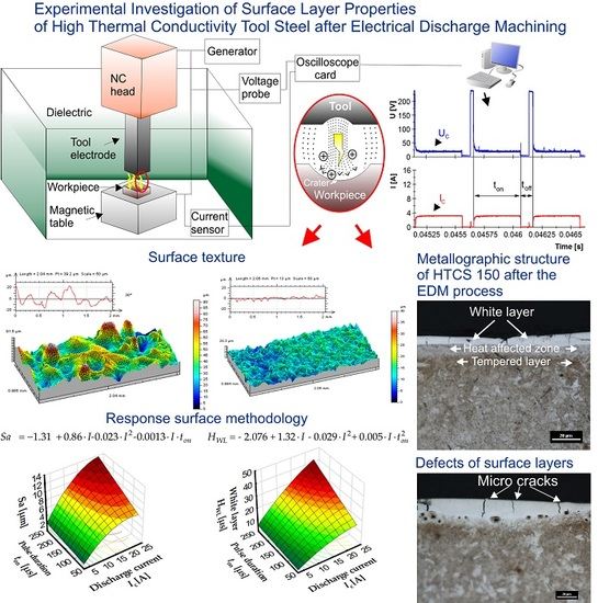
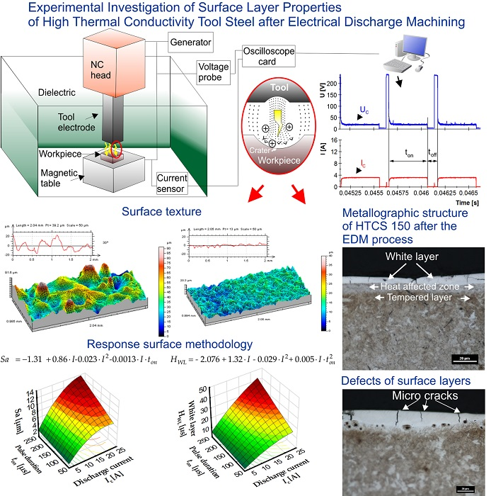
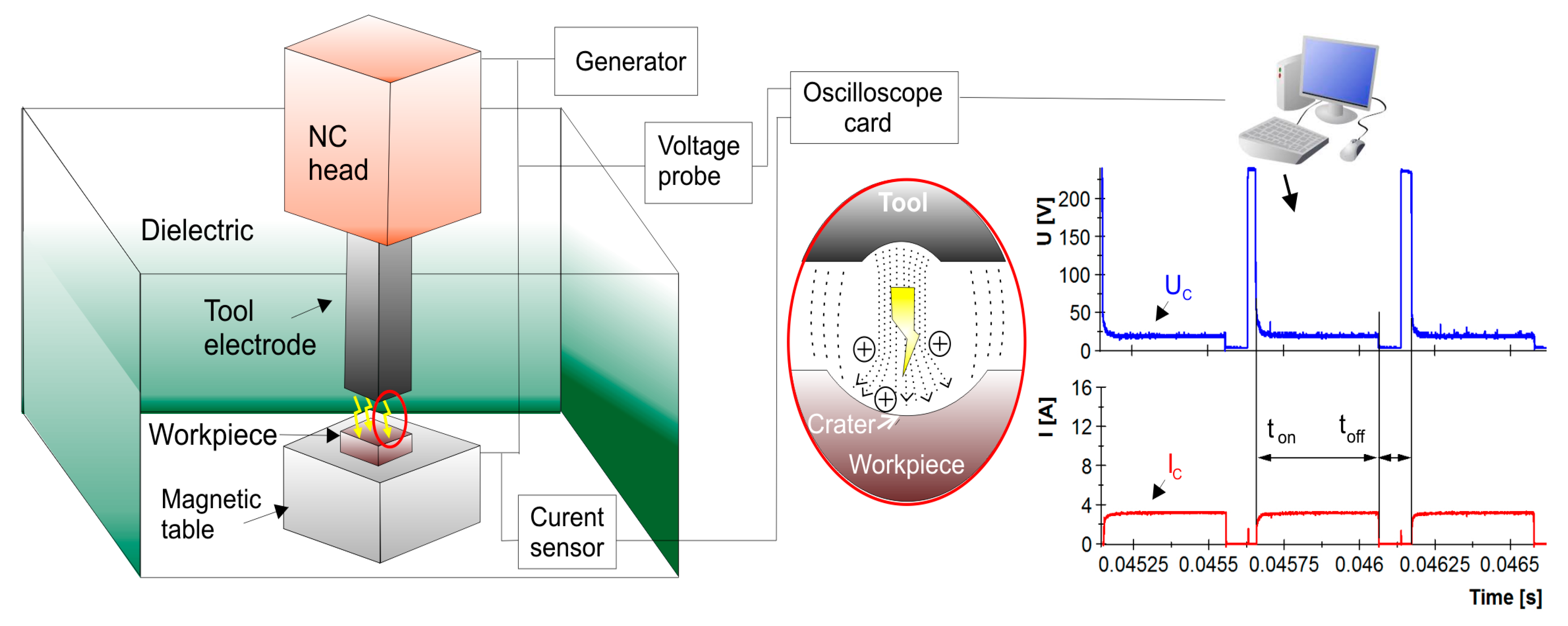
2.1. Measurement Circuit of Voltage Current Waveforms

Measurement circuit has been developed to monitor the current-voltage characteristics during machining (Figure 1). Waveforms can be characterized by the following parameters:
  • Ic: height of the peak current during discharging;
  • Uc: discharge voltage;
  • ton: pulse duration time, the time required for the current to rise and fall during discharging; and
  • toff: time interval, which is the time from the end of one pulse to the beginning of the next pulse with the current.
The discharge voltage Uc is the main influence on the size of the gap between the electrodes. For higher discharge voltage, ionization of plasma channel occurs in the larger distance between electrodes. Discharge current Ic, pulse duration time ton, along with discharge voltage defines the energy of the electrical discharge which is described in Equation (1):
E = 0 t on U c ( t ) × I c ( t ) d t ( mJ ) ,
The experimental study on the influence of the EDM process parameters meant that pulse current (Ic) and pulse duration (ton) on the surface layer properties of HTCS 150 was conducted. The selected process parameters according to Equation (1) defined the discharge energy (for constant voltage) and mainly influenced the physical phenomenon of removing material. Time interval toff was responsible for the stabilizing conditions in the gap (removal of erosion products and deionization of the discharge channel).

2.2. Experimental Design

The study was conducted on the basis of the experimental design, which was five levels and two parameters. Conducting experiments with this methodology allowed us to reduce the number of experimental runs required to generate sufficient information for a statistically adequate result. Experiments were conducted with the following machining conditions: pulse current in the range Ic = 3–24 A, pulse duration in the range ton = 50–250 µs, with hold constants (open voltage U0 = 225 V, discharge voltage Uc = 25 V) and time interval toff = 0.3 ton. Table 1 shows the levels of machining parameters carried out in the experimental design.
The range of analyzed parameters in the design experiment was selected on the basis of the literature and a conducted preliminary study based on the stability of the occurring discharges (monitored in the developed circuit).
Experimental investigation of the influence of the EDM process parameters on the surface layer properties of high thermal conductivity tool steel was carried out using response surface methodology (RSM). RSM is a mathematical and statistical technique that uses regression analysis to build an empirical model on the influence of several variables for the investigated object. Using this methodology, a near optimal point can be achieved.
In RSM, the influence of the independent process parameters on the investigated parameters can be written as:
Y = f (X1, X2, …, XN) ± ε
where Y is the response; f is the response function; ε is the experimental error; and X1, X2, X3, ..., Xn are independent parameters.

2.3. Measuring Surface Layer Properties

Investigation of the surface layers properties of HTCS 150 after the EDM was carried out was undertaken on a Taylor-Hobson FORM TALYSURF Series 2 scan profilometer (Taylor Hobson, Leicester, UK) and optical microscope (Nikon, Tokyo, Japan). To investigate the surface roughness, an area of 1 × 4 mm was measured with discretization step (10 μm) in the X-axis and Y-axis. To characterize the surface texture after the EDM, the following 3D parameter surface roughness was used:
  • arithmetic mean of the deviations from the mean Sa (average value of the absolute heights over the entire surface). The Sa parameter responds to the 2D roughness profile parameters Ra. It may be obtained by adding the individual height values without regard to sign and dividing the sum by the number of the data matrix, where M is the number of points per profile, N the number of profiles and z, x, y are the height of the profile at a specific point.
    S a = 1 N M x = 0 N = 1 y = 0 M = 1 | z x , y |
  • density of the top Sds (a number of summits of a unit sampling area), which relies on the eight nearest neighbor summit definition where a peak is defined if it is higher than its eight nearest neighbors:
    S d s = 1 n u m b e r   o f   s u m m i t s ( M 1 ) ( N 1 ) Δ x Δ y
  • arithmetic mean curvature to the top Ssc. This parameter obtains the mean form of the peaks which are pointed or rounded, according to the mean value of the curvature of the surface at these points.
Metallographic surface structure studies were performed using a NIKON Eclipse LV 150 optical microscope (Nikon, Tokyo, Japan) coupled to an NIS-Elements BR 3.0 image analyzer (Nikon, Tokyo, Japan). Specimens were included in the resin; next, they were machined with grinding and polishing. Micro-etching was performed with nital 5% to reveal the microstructure of the material.

3. Results and Discussions

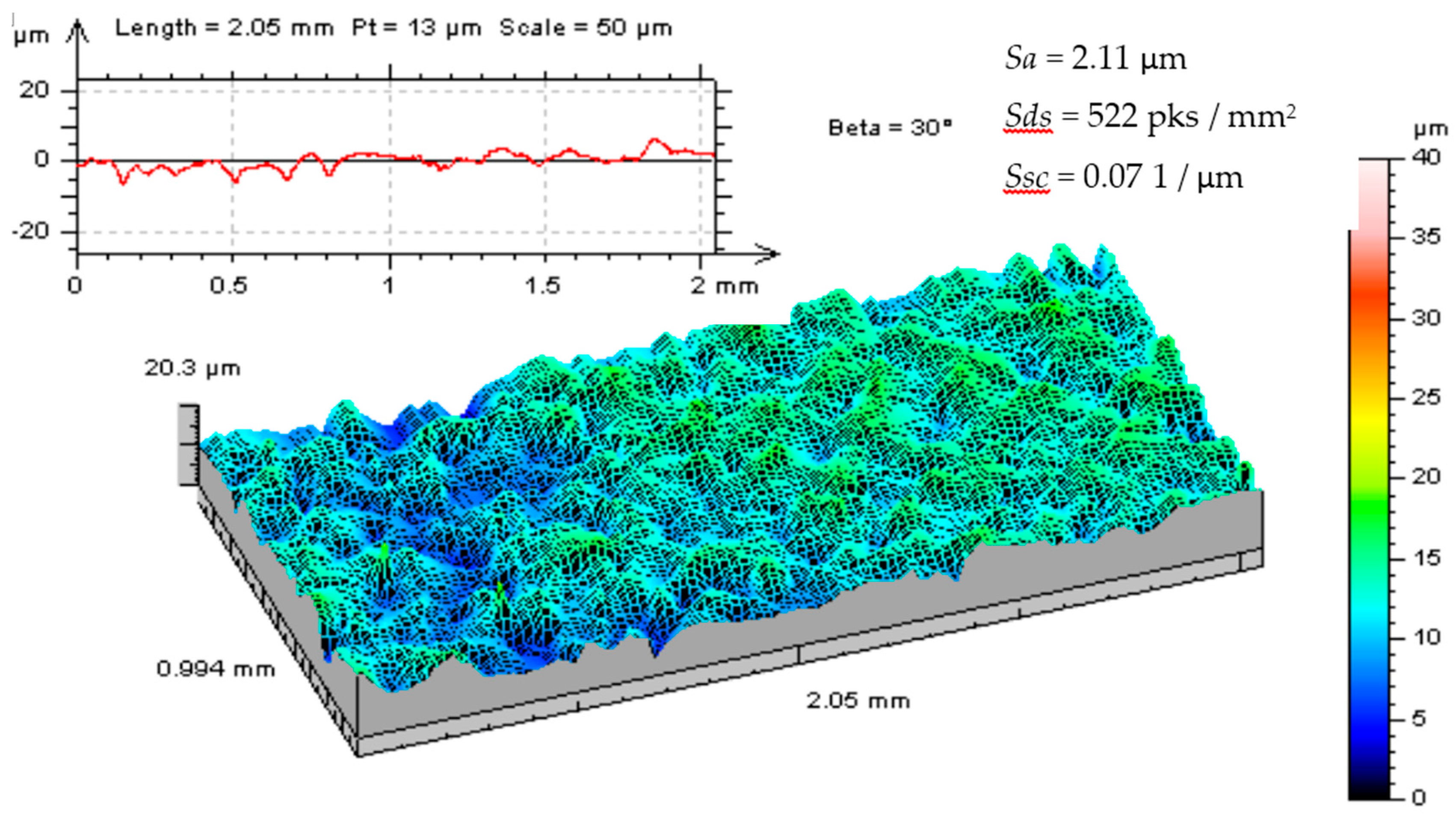
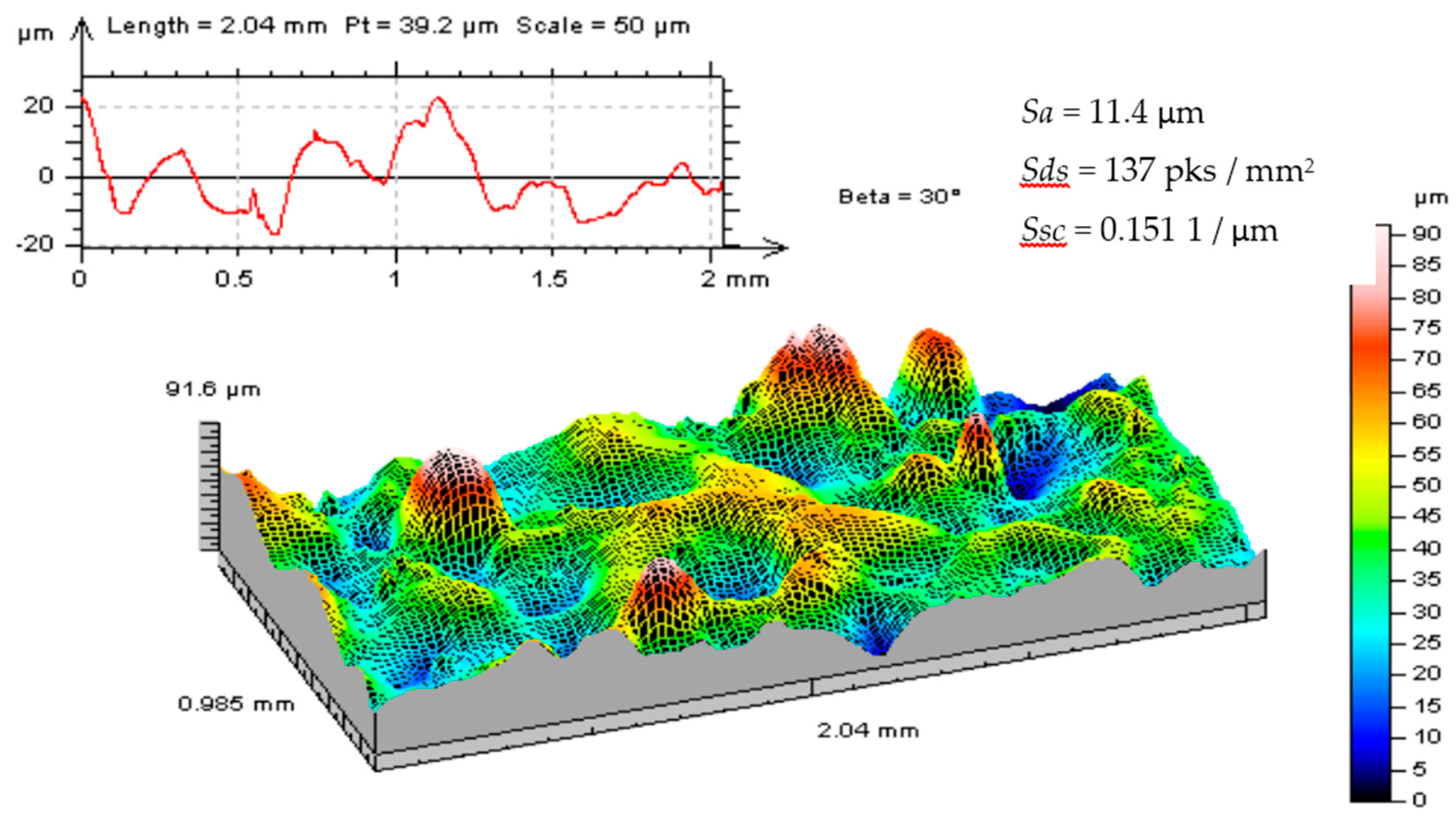
3.1. Surface Texture

The outer part of the top layer is determined by the topography of the surface. The surface texture is generated by traces of electrical discharges. Depending on the investigated EDM process parameters, there were significant differences in surface texture properties. The influence of the two major EDM parameters were investigated: pulse current in the range Ic = 3–24 A and pulse duration in the range ton = 50–250 µs, which determine the energy of the discharge pulse (with constant voltage). The experimental research on the influence of EDM process parameters on the surface roughness was carried out in accordance with the central composite rotatable design of the experiment with two factors and five levels. The selection of this type of experiment allowed us to investigate the two factors at each of the five levels. Conducting experiments with the central composite design allowed us to reduce the number of experimental runs required to generate sufficient information for a statistically adequate result. The results of the experimental studies are presented in Table 2.
The surface texture after EDM was formed by the overlapping of craters of electrical discharges and had a random nature. The arithmetic mean of the deviations from the mean Sa was in the range of 2.11–11.8 µm and corresponded to the values obtained in the finishing and roughing treatment. For the obtained similar value of surface roughness parameter Sa for Samples 7 and 3, the value of the density of the top Sds showed quite significant differences. This is due to the fact that the Sds parameter depends on both the amplitude of the roughness and the distance between summits. The surface hybrid roughness parameter Sds represents a number of summits in a unit sampling area and indirectly define the distance between the next summits. A higher value of Sds means that the same area has more summits. The changed distance between the next summits with a similar value of roughness height parameters can show that the crater has a similar height but different diameter.
The arithmetic mean curvature to the top Ssc was in the range of 0.07–0.153 1/µm. The larger value of the Ssc meant that the vertices were rounded. The Sds and Ssc values had a significant effect on the abrasive wear of the surface, the application of coatings and reflectivity. With a smaller rounding radius of the vertices, the top had a sharpness edge, which caused an increase in the surface adhesion.
Analysis of the 3D measured surface texture (Figure 2 and Figure 3) showed that the shape and depth of the craters was dependent from the investigated EDM parameters.

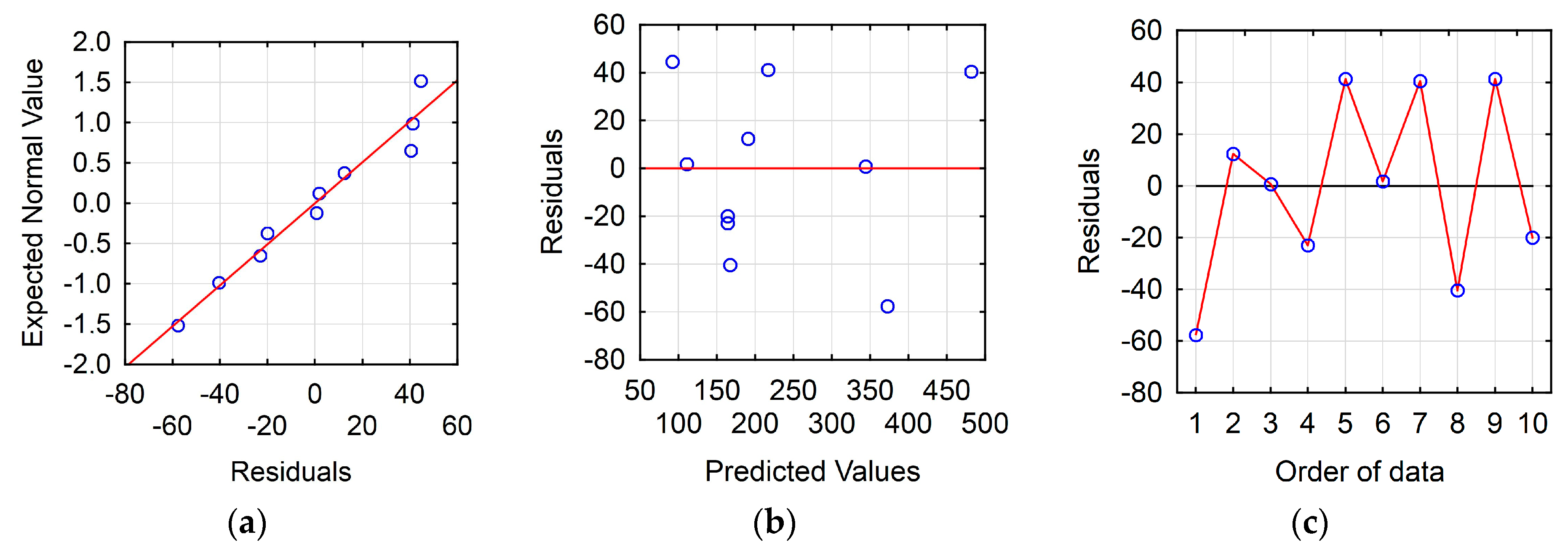
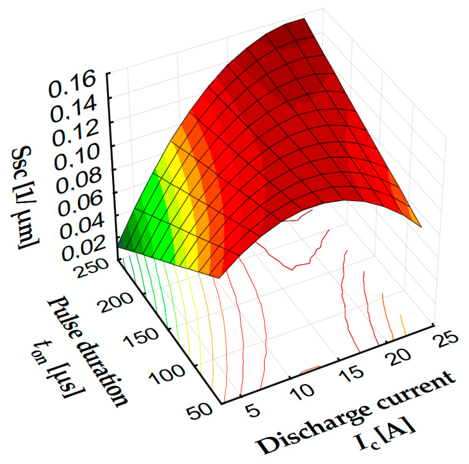
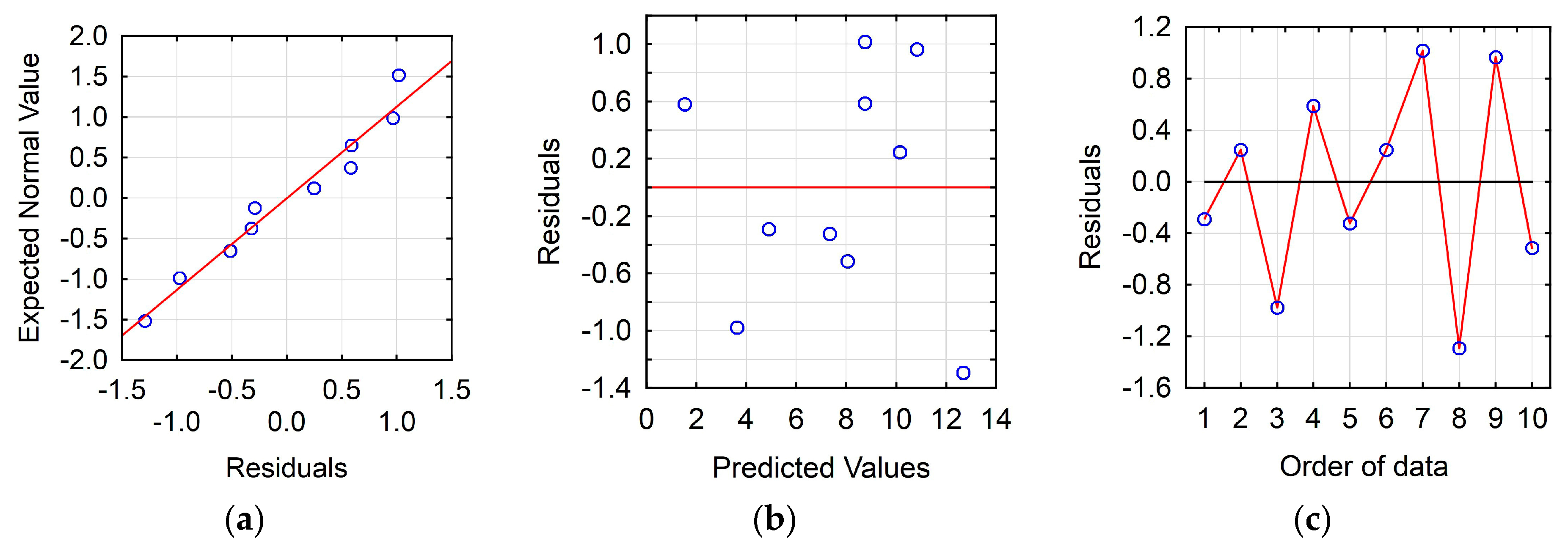
3.2. Modeling Surface Roughness Parameters Using Response Surface Methodology

Response surface methodology allows a process by a different function to be modeled. The choice of the function should consider a best fit of the experimental results for response function (the investigated parameters). Considering the above assumption, a regression equation was described by the polynomial function of the second degree:
Y = β 0 + i = 1 k β i X i + i = 1 k β i i X i 2 + i = 1 , i j k β i j i X i X j + ε
This function allows the region of interest to be located where the response reaches its optimum or near optimal value.
Results from the experimental studies were used to build an empirical model of influence discharge current Ic and pulse duration ton on the surface roughness parameters. The statistical test of the bullied model was conducted. The degree of fit of the regression equation to the results of the experimental studies described the ratio correlation R. The ratio R was in the range R є < 0, 1 > and reflected the variability of the investigated characteristic. If the value of the coefficient R approached unity, it was a more accurate fit of the regression equation to the research results. The Fishera-Snedecora test (F) was used to verify the significance of the obtained correlation coefficient R. The test allowed us to assess the adequacy of the regression equation, in other words, the compatibility of the model with the results obtained during the experimental research. The value of the function test F was calculated and compared with the critical value of the tables Fkr (read for the number of freedom at an established level of significance p). The correlation coefficient R was significant when there was a relation for the associated p-value (p = 0.05):
F F kr
The signification of each term in the regression equation was checked with a test of t-students. The value of the function test t was calculated and compared with the critical value of the tables tkr (read for the number of freedom at an established level of significance p).The term of the equation was significant when there was a relation for the associated p-value (p = 0.05):
t t kr
After eliminating the non-significant terms, the final response equations for the surface roughness parameters were described by the polynomial function of the second degree, which is presented in Equations (8)–(10). Table 3 presents the regression summaries for the established equations.
S a = 1.31 + 0.86 × I 0.023 × I 2 0.0013 × I × t on
S d s = 631.3 40.40 × I + 1.45 × I 2 0.39 × I × t on
S s c = 0.113 + 0.0076 × I 0.0006 × t on 2 0.0004 × I 2 + 0.00004 × I × t on
Developed models of the surface roughness parameters after EDM were checked by a residual normal probability plot, the residuals versus the predicted values and the residuals versus the order of data. The investigated normal probability plots in Figure 4a, Figure 5a and Figure 6a show that the relationship between the expected normal value and residuals was approximately linear, which indicated that the residuals may have normal distributions. An analysis of the residuals versus the predicted values (Figure 4b, Figure 5b and Figure 6b) showed that the residuals had a stochastic nature. Observed errors had a random pattern around the center line and were not correlated with another variable or with each other. The study of residuals versus the order of data (Figure 4c, Figure 5c and Figure 6c) showed that the error terms were independent of one another. The developed models were correct on average for the predicted values.
The value of R was over 96% which meant that the regression models provided a good explanation of the relationship between the investigated parameters discharge current Ic, pulse duration ton and the surface roughness parameters. The associated p-value for the model was 0.05 (95% confidence). Figure 7 and Figure 8 show the estimated response surface for the surface roughness parameters in relation to the discharge current Ic and pulse duration ton.
The parameter describing the average height of surface roughness Sa (Figure 7a) was mainly dependent on the discharge current. The increased current and pulse time corresponded to an increase in the amount of eroded material in a single impulse. The craters generated by the electrical discharges were characterized by a larger diameter and depth. This led us to obtain a higher value of roughness height parameter Sa. At low currents (about 3 A), increasing the discharge time (and therefore discharge energy) did not result in a significant increase in the Sa parameter. This was related to the amount of heat generated and supplied to the workpiece during the discharge process, which caused melting and evaporation of the material. The shape and evolution of the plasma channel radius is dependent on pulse time. Increasing pulse time at the lowest current caused the generation of craters with a larger diameter but with an unchanging depth. The shape of the roughness vertices can be described by the arithmetic mean curvature to the top of Ssc and the density of the top Sds. The value of these parameters is dependent on both the discharge current and the pulse time. For the highest values of discharge current and pulse time, the lowest density of the top Sds and heights value of roughness parameters Ssc (Figure 8) and Sa were obtained. This meant that the crater generated by the electrical discharges had the largest diameter and height and the vertices were rounded. Overlapping individual traces of the discharges built the surface texture. The increased current and pulse time increased the diameter and power of the plasma channel. This led to a higher roughness profile with larger distances between the individual vertices and rounded tops. For short pulse times and the smallest current values, the surface texture was characterized by a high density of vertices with sharpened edges.

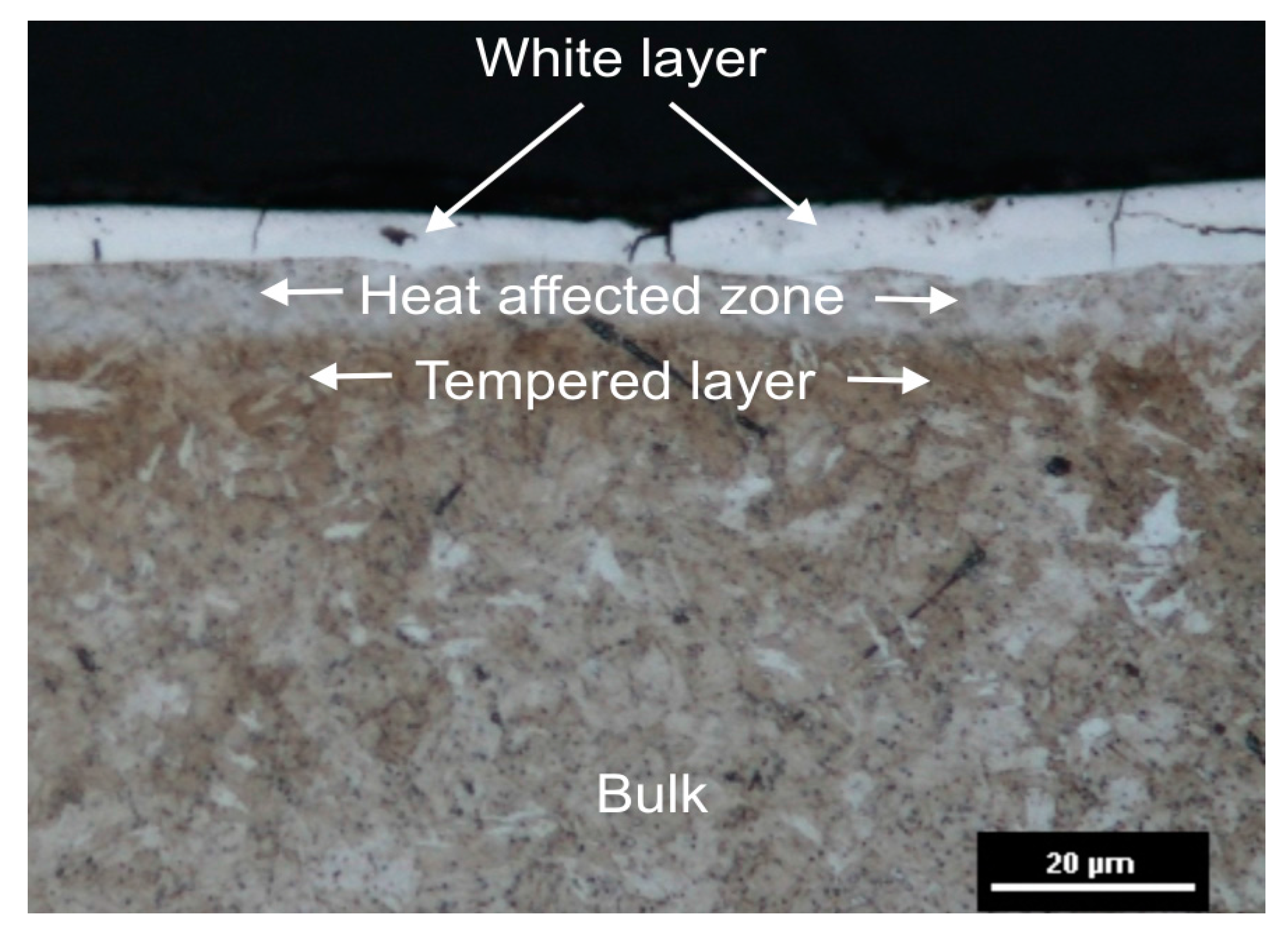
3.3. Surface Layer Properties

The thermal, chemical and mechanical processes occurring during the electrical discharges create specific surface layer properties. On the basis of the analysis of the metallographic surface of the machined samples, the appearance of characteristic layers was observed (Figure 9). The external melting layer (WL) and heat affected zones, which were visible in the form of a light structure directly under the melted layer, had structural members oriented along the heat dissipation direction (perpendicular to the surface to be treated) and tempered layer, occurring as a dark streak.
Electrical discharges occurring in the gap cause melting and evaporation of both the workpiece and the working electrode. At the end of the discharges, melted materials—which are a collapsed bubble around the plasma channel—is ejected to the gap. This melted material—that is not removed from the crater—re-solidifies, therefore creating the white layer. This layer in structure may be a chemical decomposition from both the core material and the working electrode. Under the melted layer was the heat affected zone (HAZ). This layer was visible in the form of a bright structure directly under the melted layer, which had structural elements oriented along the heat-dissipating direction (perpendicular to the surface to be treated). This layer was composed of martensitic and residual austenite. The specific structure was formed by the diffusion of carbon from the pyrolysis of the oil and rapid heat dissipation. Under the HAZ, there was a tempered zone. The tempered layer was formed by the influence of discharge energy which caused the heating of this material zone, which was then cooled by transporting the heat to the bulk. The occurrence of individual layers was observed for all samples.
The main elements of the surface layers that has an influence on the properties of surface integrity are the thickness of the white layer. Experimental research into the influence of EDM process parameters on the thickness of the white layer was carried out in accordance with the central composite design of experiment of two factors and five levels. The thickness of the white layer was measured in 10 sections for each sample. The machining parameters used in the design of the experiment and measured thickness of the white layer are presented in Table 4.

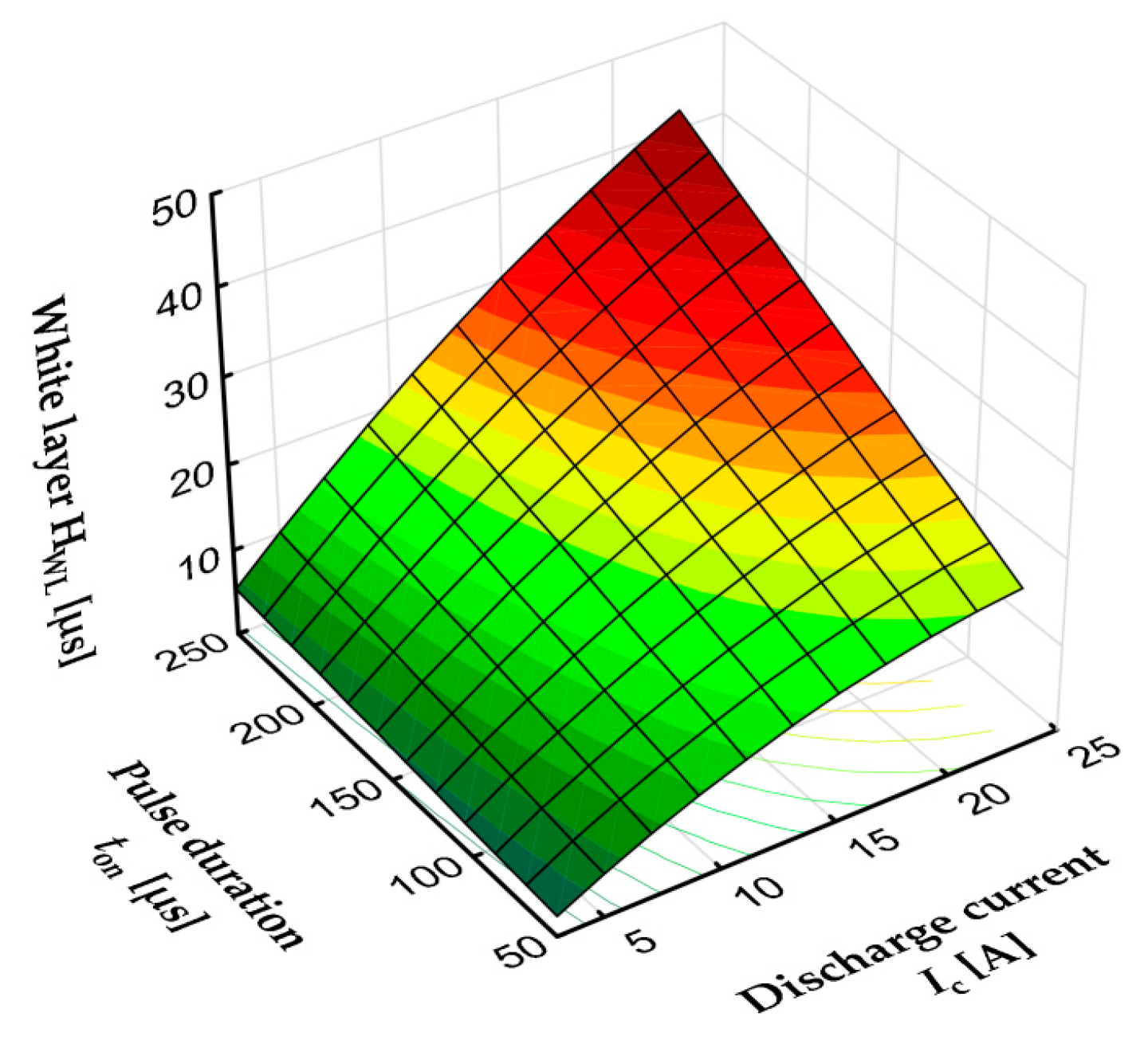
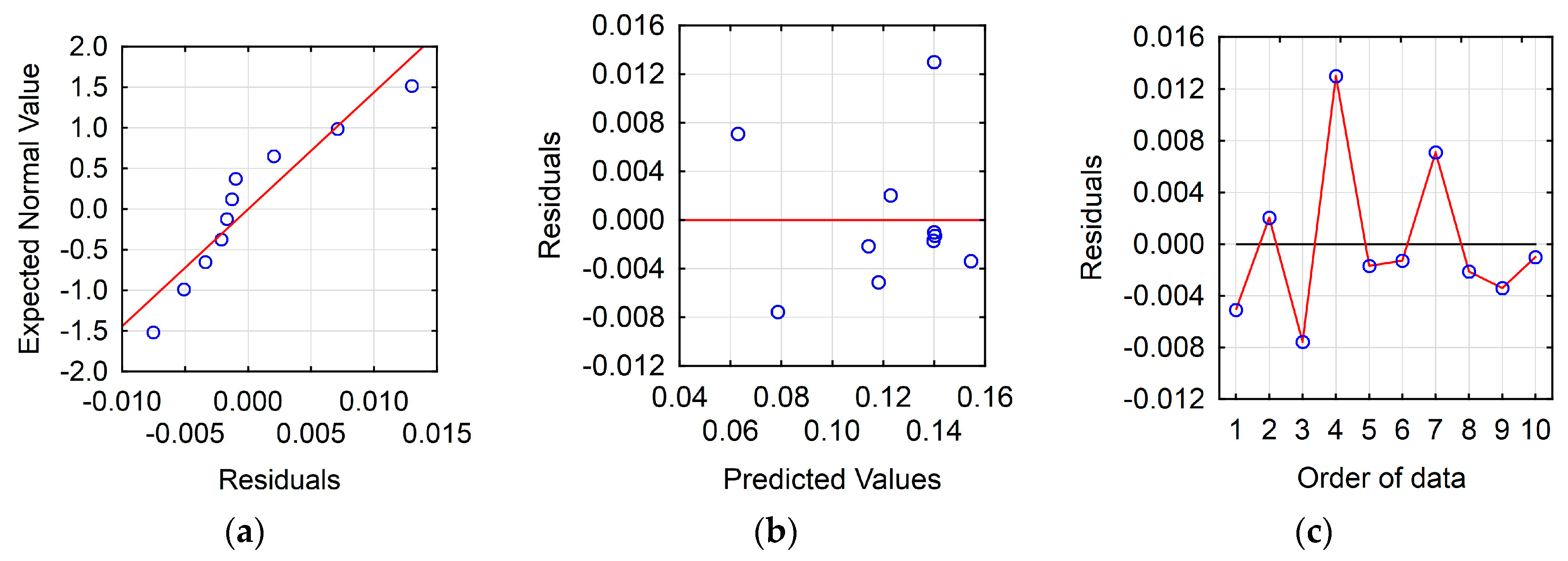
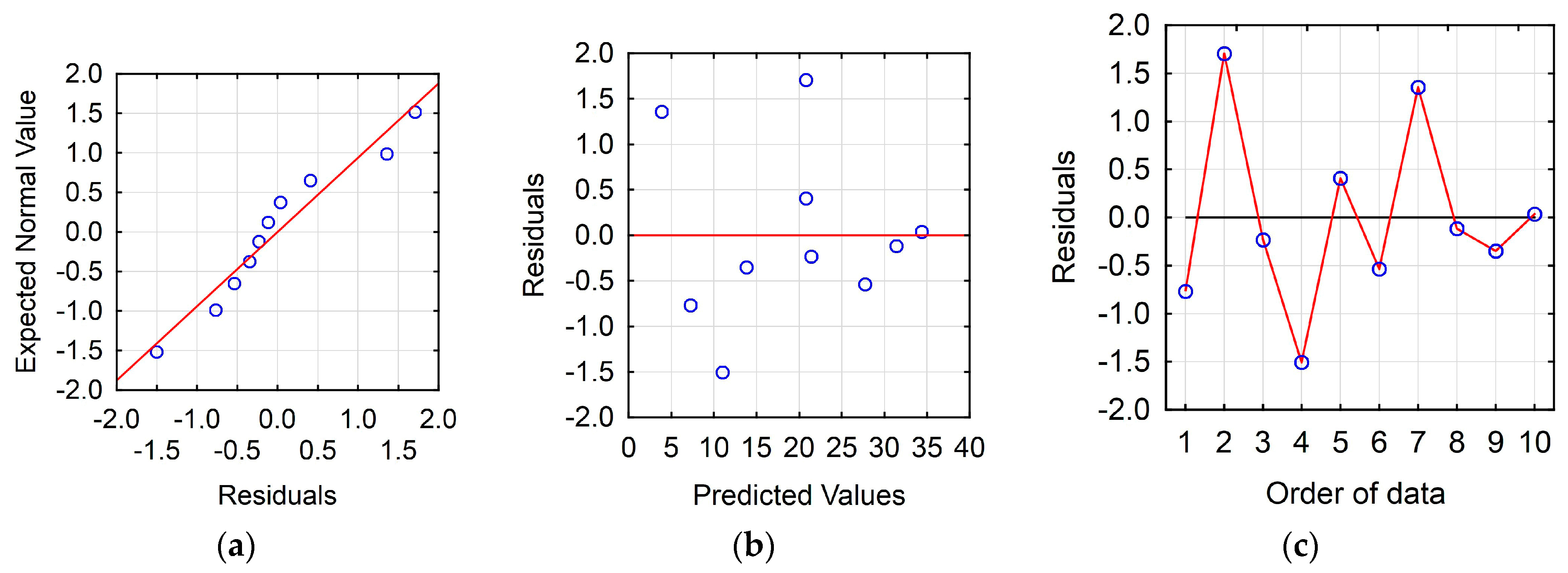
3.4. Modeling of White Layer Thickness Using Response Surface Methodology

According to the described response surface methodology based on the results of the experimental studies, an empirical model for the white layer thickness was developed. After eliminating the non-significant terms, the final response equation for the average white layer thickness was described by the polynomials function of the second degree Equation (11). Table 5 presents the regression summaries for the established equation.
H WL = 2.076 + 1.32 × I 0.029 × I 2 + 0.005 × I × t on 2
The developed model of the white layer thickness was checked by the analysis of the residual normal probability plot, the residuals versus the predicted values and the residuals versus the order of data. The relationship between the expected normal value and residuals was approximately linear, which indicates that the residuals may have normal distributions (Figure 10a). The residuals versus the predicted values had a random nature (Figure 10b). The plot of the residuals versus the order of data (Figure 10c) showed that errors were independent of each another.
The value of R was over 99%, which meant that the regression model provided an excellent explanation of the relationship between the investigated parameters of discharge current Ic, pulse duration ton and the average white layer thickness. The associated p-value for the model was 0.05 (95% confidence).
The average thickness of the white layer was mainly dependent on the amount of thermal energy supplied to the workpiece. Increasing the pulse time at the lowest current did not significantly change the HWL value. In this case, most of the discharge energy was conducted to the material, which caused a small amount of eroded material. Increase pulse time and current caused an increase in the amount of fused and evaporated material, consequently, more material that was not removed from the surface of workpiece re-solidified on the core. Figure 11 shows the estimated response surface for the average white layer thickness in relation to the design parameters of discharge current Ic and pulse duration ton.

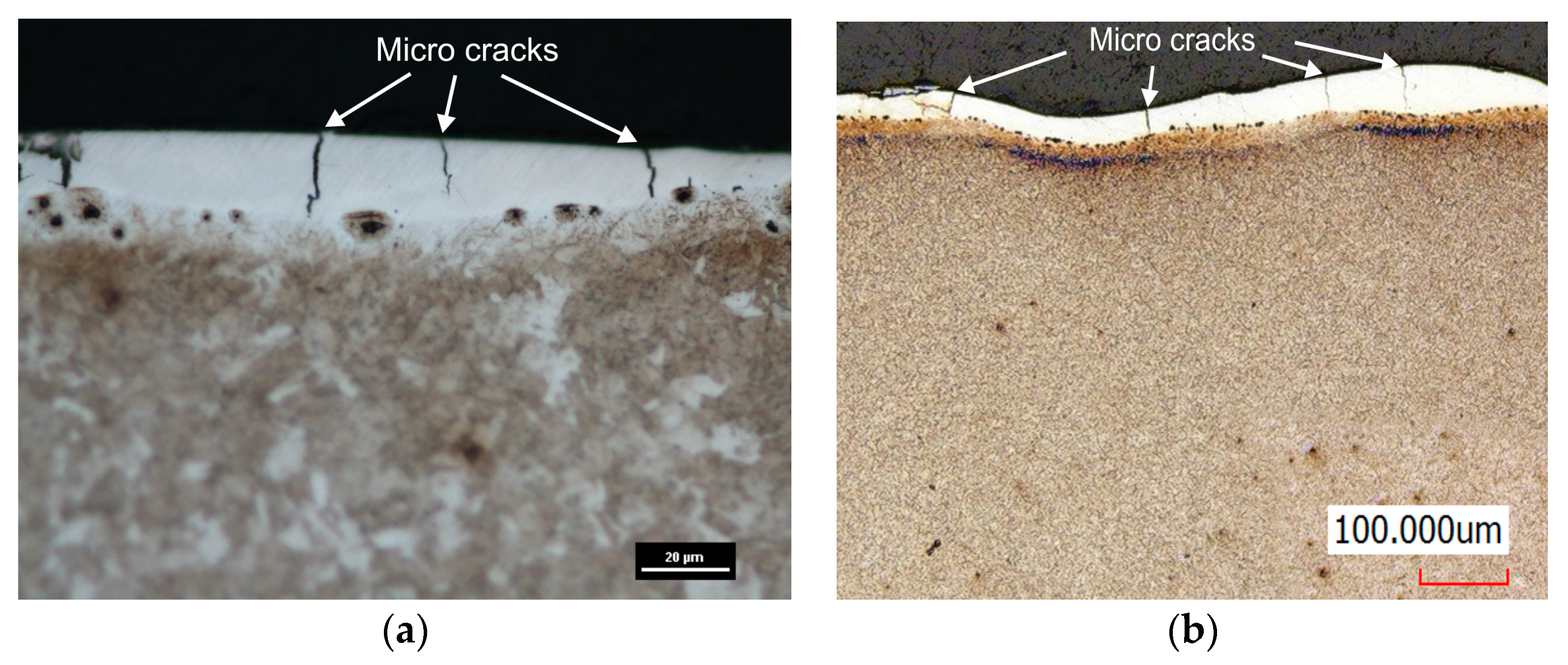
3.5. Defects of Surface Layers: Micro Cracks

The physical phenomenon of removal material in the EDM generates microstructure defects in material such as micro cracks. The energy of the electrical discharge leads to local melting and evaporation of material. Between the electrodes, a plasma channel is formed around bubbles filled with vaporized metals. An implosive closing of the plasma channel and bubbles leads to throwing away erosion products to the gap. Part of the molten material that was not removed from the crater, rapidly re-solidifies in the core which causes thermal stress. Tensile stress is generated by the result of the rapid cooling and solidification of the molten layer at the much lower temperature of the core material. Shrinkage is produced by the resist of the core material. Exceeding the maximum tensile strength of the material, causes the generation of micro cracks (Figure 12). These surface structure defects strongly influence fatigue resistance and corrosion resistance.
Analysis of images of the metallographic structure from conducted experimental research revealed that in each sample, micro cracks were found. Micro cracks mostly occur on the surface of the crater and are usually directed perpendicular to the heat affected zone. In most of the investigated samples, micro cracks propagated to the end of the white layer.

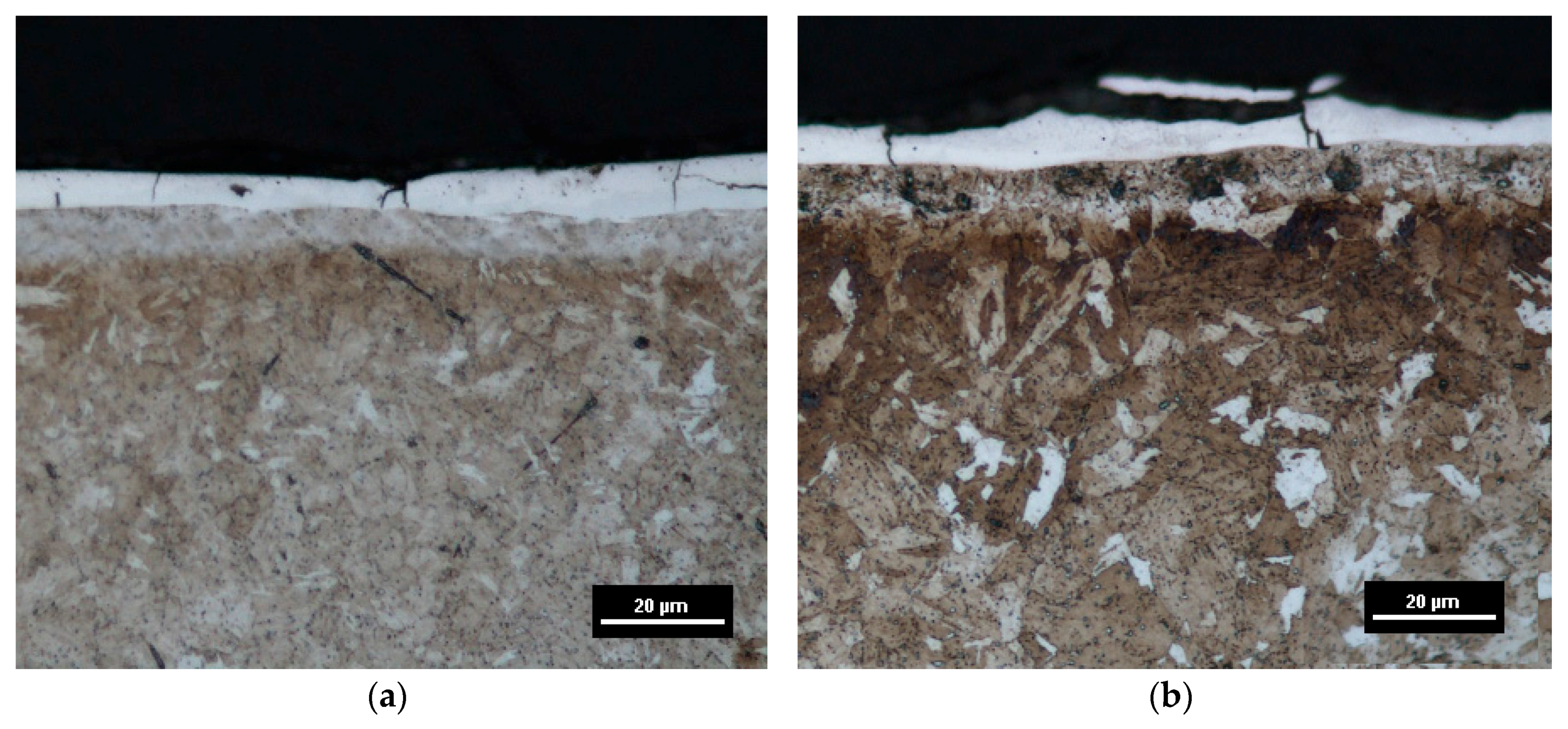
3.6. Influence of Sequential Machining on Surface Layers Properties

The industrial manufacture of parts with EDM technology is divided into several treatments. In the first stage, material is removed from the workpiece using the biggest discharge energy (roughing technology). In the next step, the parameters of the process are changed to achieve the proper surface layer properties and low roughness of the manufactured parts. The EDM process is conducted with the semi finishing and finishing step with respectively smaller discharge energy.
In addition to the studies conducted with an experimental methodology design, sequential processing of EDM has been carried out to investigate the metallographic structure typical for production processes where roughing, semi finishing and finishing operations occur. Table 6 presents the investigated processing.
A comparative analysis of metallographic images (Figure 13) was performed for the sample to be treated sequentially and for Sample 7 of the experimental design, which corresponded to the finishing stage.
The average thickness of the white layer of the sample by sequential manufacturing was about to HWL = 5.5 μm and it corresponded to the average layer thickness obtained for Sample 7. Additionally, the average layer thickness of the heat-affected zone (HAZ) for both samples was similar and was equal to HHAZ = 6–7 μm. Significant differences in the analyzed samples were obtained in the thickness of the tempered zone. The sequentially processed sample had a twice the thickness of the tempered layer (HT = 20 μm) from sample processing with only the finishing parameters. The heat flux of the sample processed in sequential order left changes in the thickness of the tempered layer.

4. Conclusions

The experimental studies conducted were focused on the surface layer properties of high thermal conductivity tool steel HTCS 150 after electrical discharge machining. As a result of the energy supplied by the electrical discharges, craters formed a specific surface texture. Surface roughness parameters directly depend on the form discharge current and time pulse. Heat flux from the discharge causes changes in the surface integrity. Observation of the metallographic structure showed that the workpiece had characteristic layers such as the external melting layer (white layer), heat affected zones and tempered layer. The newly formed metallographic structure was characteristic of the EDM process and the thickness of the individual layers was dependent on the machining parameters that defined the amount of energy transferred to the workpiece. The physical phenomenon of material removal in EDM led to the generation of microstructure defects in the material such as micro-cracks.
To summarize the results of the experimental investigation:
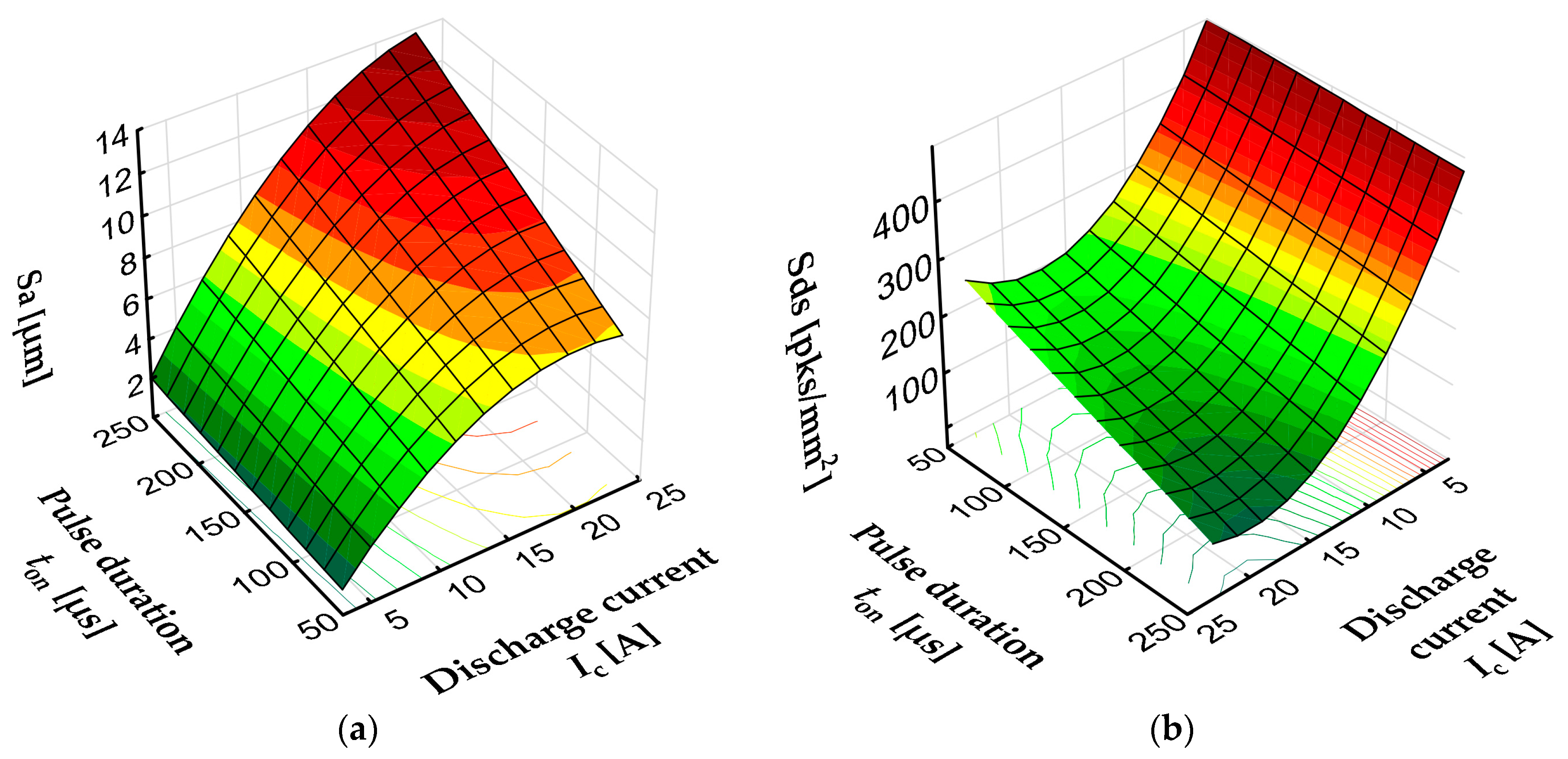
  • The roughness parameter Sa was the range of 2.11–11.8 µm and corresponded to finishing and roughing machining. Sa was mainly dependent on the discharge current. Furthermore, the increase of discharge current increased the amount of eroded material in a single pulse, thus leading to higher roughness.
  • Surface roughness hybrid parameters Sds and Ssc described the shape of the roughness vertices. The arithmetic mean curvature to the top Ssc was in the range of 0.07–0.153 1/µm and the density of the top Sds was in the range of 113–522 pks/mm2. For the highest values of discharge current and pulse time, the lowest density of the top Sds and the height values of the roughness parameters Ssc and Sa were obtained. The increase in discharge current and pulse time caused increases in the amount of eroded material, which provided a higher roughness profile with larger distances between the individual vertices and rounded tops. For finishing parameters with the shortest pulse times and the smallest current values, the surface roughness was characterized by a high density of vertices with sharpened edges.
  • The thermal, chemical and mechanical processes occurring during the electrical discharges caused the creation of a surface layer containing a white layer, heat affected zones and a tempered layer. The thickness of each layer depended on the discharge current and pulse time. A minimal thickness of the investigated layers was observed for the lowest discharge energy.
  • The main elements of the surface layers that influence the surface integrity properties are the thickness of the white layer. The average thickness of the white layer was in the range of 5–34.5 µm and depends mainly on the amount of thermal energy supplied to the workpiece. Increasing the pulse time at the lowest current did not significantly change the HWL value.
  • Images of the metallographic structure showed defects in the surface layers as micro cracks. The micro cracks mostly occurred on the surface of the crater and were usually directed perpendicular to the heat affected zone.
  • Sequential processing of the EDM typical for production processes such as roughing, semi-finishing and finishing operations, showed that the average thickness of the white layer of sample sequential manufacturing was equal to HWL = 5.5 μm. This value corresponded to the average layer thickness obtained in single finishing processing but had a twice as large thickness of the tempered layer (HT = 20 μm). These differences were a result of the residue after the heat flux in the roughing operation and could be minimized by the appropriate selection of finishing parameters.
  • Developed regression equations can be used in electrical discharge machining as a guideline for the selection of process parameters to achieve the desired surface layers properties.

Acknowledgments

This research work was supported by a grant from the Fundamental Research Funds of the Faculty of Production Engineering, Warsaw University of Technology, No. 504/03142/1104/42.000100.

Author Contributions

Rafał Świercz and Dorota Oniszczuk-Świercz conceived and designed the experiments; Rafał Świercz performed the experiments; Rafał Świercz and Dorota Oniszczuk-Świercz analyzed the data; and Rafał Świercz wrote the paper.

Conflicts of Interest

The authors declare no conflict of interest.

References

  1. Skoczypiec, S.; Ruszaj, A. A sequential electrochemical–electrodischarge process for micropart manufacturing. Precis. Eng. 2014, 38, 680–690. [Google Scholar] [CrossRef]
  2. Sawicki, J.; Paczkowski, T. Effect of the hydrodynamic conditions of electrolyte flow on critical states in electrochemical machining. EPJ Web Conf. 2015, 92, 02078. [Google Scholar] [CrossRef]
  3. Rajurkar, K.P.; Sundaram, M.M.; Malshe, A.P. Review of Electrochemical and Electrodischarge Machining. Procedia CIRP 2013, 6, 13–26. [Google Scholar] [CrossRef]
  4. Oniszczuk-Świercz, D.; Świercz, R. Surface texture after wire electrical discharge machining. In Proceedings of the 26th International Conference on Metallurgy and Materials, Brno, Czech Republic, 24–26 May 2017. in press. [Google Scholar]
  5. Krajewski, A.; Włosiński, W.; Chmielewski, T.; Kołodziejczak, P. Ultrasonic-vibration assisted arc-welding of aluminum alloys. Bull. Pol. Acad. Sci. Tech. Sci. 2013, 60, 841–852. [Google Scholar] [CrossRef]
  6. Chmielewski, T.; Golański, D.; Włosiński, W.; Zimmerman, J. Utilizing the energy of kinetic friction for the metallization of ceramics. Bull. Pol. Acad. Sci. Tech. Sci. 2015, 63, 201–207. [Google Scholar] [CrossRef]
  7. Gostimirovic, M.; Kovac, P.; Sekulic, M.; Skoric, B. Influence of discharge energy on machining characteristics in EDM. J. Mech. Sci. Technol. 2012, 26, 173–179. [Google Scholar] [CrossRef]
  8. Świercz, R.; Oniszczuk-Świercz, D. Influence of electrical discharge pulse energy on the surface integrity of tool steel 1.2713. In Proceedings of the 26th International Conference on Metallurgy and Materials, Brno, Czech Republic, 24–26 May 2017. in press. [Google Scholar]
  9. Ho, K.H.; Newman, S.T. State of the art electrical discharge machining (EDM). Int. J. Mach. Tools Manuf. 2003, 43, 1287–1300. [Google Scholar] [CrossRef]
  10. Marashi, H.; Jafarlou, D.M.; Sarhan, A.A.D.; Hamdi, M. State of the art in powder mixed dielectric for EDM applications. Precis. Eng. 2016, 46, 11–33. [Google Scholar] [CrossRef]
  11. Hui, Z.; Liu, Z.; Cao, Z.; Qiu, M. Effect of Cryogenic Cooling of Tool Electrode on Machining Titanium Alloy (Ti–6Al–4V) during EDM. Mater. Manuf. Process. 2016, 31, 475–482. [Google Scholar] [CrossRef]
  12. Dewangan, S.; Biswas, C.K.; Gangopadhyay, S. Influence of Different Tool Electrode Materials on EDMed Surface Integrity of AISI P20 Tool Steel. Mater. Manuf. Process. 2014, 29, 1387–1394. [Google Scholar] [CrossRef]
  13. Cusanelli, G.; Hessler-Wyser, A.; Bobard, F.; Demellayer, R.; Perez, R.; Flükiger, R. Microstructure at submicron scale of the white layer produced by EDM technique. J. Mater. Process. Technol. 2004, 149, 289–295. [Google Scholar] [CrossRef]
  14. Shrestha, T.; Alsagabi, S.F.; Charit, I.; Potirniche, G.P.; Glazoff, M.V. Effect of Heat Treatment on Microstructure and Hardness of Grade 91 Steel. Metals 2015, 5, 131–149. [Google Scholar] [CrossRef]
  15. Spadło, S.; Kozak, J.; Młynarczyk, P. Mathematical Modelling of the Electrical Discharge Mechanical Alloying Process. Procedia CIRP 2013, 6, 422–426. [Google Scholar] [CrossRef]
  16. Spadło, S.; Młynarczyk, P.; Łakomiec, K. Influence of the of electrical discharge alloying methods on the surface quality of carbon steel. Int. J. Adv. Manuf. Technol. 2017, 89, 1529–1534. [Google Scholar] [CrossRef]
  17. Radziejewska, J. Influence of laser-mechanical treatment on surface topography, erosive wear and contact stiffness. Mater. Des. 2011, 32, 5073–5081. [Google Scholar] [CrossRef]
  18. Murray, J.W.; Clare, A.T. Repair of EDM induced surface cracks by pulsed electron beam irradiation. J. Mater. Process. Technol. 2012, 212, 2642–2651. [Google Scholar] [CrossRef]
  19. Radziejewska, J.; Skrzypek, S.J. Microstructure and residual stresses in surface layer of simultaneously laser alloyed and burnished steel. J. Mater. Process. Technol. 2009, 209, 2047–2056. [Google Scholar] [CrossRef]
  20. Kim, J.-M.; Ha, T.-H.; Park, J.-S.; Kim, H.-G. Effect of Laser Surface Treatment on the Corrosion Behavior of FeCrAl-Coated TZM Alloy. Metals 2016, 6, 29. [Google Scholar] [CrossRef]
  21. Tabernero, I.; Lamikiz, A.; Martínez, S.; Ukar, E.; López de Lacalle, L.N. Modelling of energy attenuation due to powder flow-laser beam interaction during laser cladding process. J. Mater. Process. Technol. 2012, 212, 516–522. [Google Scholar] [CrossRef]
  22. Kozak, J.; Rozenek, M.; Dabrowski, L. Study of electrical discharge machining using powder-suspended working media. Proc. Inst. Mech. Eng. Part B J. Eng. Manuf. 2003, 217, 1597–1602. [Google Scholar] [CrossRef]
  23. Klocke, F.; Lung, D.; Antonoglou, G.; Thomaidis, D. The effects of powder suspended dielectrics on the thermal influenced zone by electrodischarge machining with small discharge energies. J. Mater. Process. Technol. 2004, 149, 191–197. [Google Scholar] [CrossRef]
  24. Lauwers, B. Surface Integrity in Hybrid Machining Processes. Procedia Eng. 2011, 19, 241–251. [Google Scholar] [CrossRef]
  25. Chmielewski, T.; Golański, D.A. New method of in-situ fabrication of protective coatings based on Fe–Al intermetallic compounds. Proc. Inst. Mech. Eng. Part B J. Eng. Manuf. 2011, 225, 611–616. [Google Scholar] [CrossRef]
  26. Chmielewski, T.; Golański, D.; Włosiński, W. Metallization of ceramic materials based on the kinetic energy of detonation waves. Bull. Pol. Acad. Sci. Tech. Sci. 2015, 63, 449. [Google Scholar] [CrossRef]
  27. Kunieda, M.; Lauwers, B.; Rajurkar, K.P.; Schumacher, B.M. Advancing EDM through Fundamental Insight into the Process. CIRP Ann. Manuf. Technol. 2005, 54, 64–87. [Google Scholar] [CrossRef]
  28. Hayakawa, S.; Kusafuka, Y.; Itoigawa, F.; Nakamura, T. Observation of Material Removal from Discharge Spot in Electrical Discharge Machining. Procedia CIRP 2016, 42, 12–17. [Google Scholar] [CrossRef]
  29. Kozochkin, M.P.; Grigor’ev, S.N.; Okun’kova, A.A.; Porvatov, A.N. Monitoring of electric discharge machining by means of acoustic emission. Russ. Eng. Res. 2016, 36, 244–248. [Google Scholar] [CrossRef]
  30. Kozochkin, M.P.; Porvatov, A.N.; Grigor’ev, S.N. Vibroacoustic Monitoring of the Major Parameters of Electrical Discharge Machining. Meas. Technol. 2017, 59, 1228–1233. [Google Scholar] [CrossRef]
  31. Spadło, S.; Dudek, D. Investigation of the shape accuracy of cylindrical holes machined by EDM process. J. Mach. Eng. 2012, 12, 98–104. [Google Scholar]
  32. Oniszczuk, D.; Świercz, R. An investigation into the impact of electrical pulse character on surface texture in the EDM and WEDM process. Adv. Manuf. Sci. Technol. 2012, 36, 43–53. [Google Scholar]
  33. Straka, L.; Corný, I.; Pitel’, J.; Hašová, S. Statistical Approach to Optimize the Process Parameters of HAZ of Tool Steel EN X32CrMoV12-28 after Die-Sinking EDM with SF-Cu Electrode. Metals 2017, 7, 35. [Google Scholar] [CrossRef]
  34. Mondal, R.; De, S.; Mohanty, S.K.; Gangopadhyay, S. Thermal Energy Distribution and Optimization of Process Parameters during Electrical Discharge Machining Of AISI D2 Steel. Mater. Today Proc. 2015, 2, 2064–2072. [Google Scholar] [CrossRef]
  35. Rahang, M.; Patowari, P.K. Parametric Optimization for Selective Surface Modification in EDM Using Taguchi Analysis. Mater. Manuf. Process. 2016, 31, 422–431. [Google Scholar] [CrossRef]
  36. Salcedo, A.T.; Arbizu, I.P.; Pérez, C.J.L. Analytical Modelling of Energy Density and Optimization of the EDM Machining Parameters of Inconel 600. Metals 2017, 7, 166. [Google Scholar] [CrossRef]
  37. Ramasawmy, H.; Blunt, L.; Rajurkar, K.P. Investigation of the relationship between the white layer thickness and 3D surface texture parameters in the die sinking EDM process. Precis. Eng. 2005, 29, 479–490. [Google Scholar] [CrossRef]
  38. Straka, Ľ.; Čorný, I.; Piteľ, J. Properties Evaluation of Thin Microhardened Surface Layer of Tool Steel after Wire EDM. Metals 2016, 6, 95. [Google Scholar] [CrossRef]
  39. Sanchez, J.A.; Pombo, I.; Cabanes, I.; Ortiz, R.; Lopez de Lacalle, L.N. Electrical discharge truing of metal-bonded CBN wheels using single-point electrode. Int. J. Mach. Tools Manuf. 2008, 48, 362–370. [Google Scholar] [CrossRef]
  40. Rovalma Company Web. Available online: http://rovalma.com/product/htcs-150/ (accessed on 1 September 2017).
Figure 1. Scheme of the electrical discharge machining (EDM) process measuring the current voltage characteristics.
Metals 07 00550 g001
Figure 2. Surface texture after EDM (Ic = 3 A, ton = 150 μs).
Metals 07 00550 g002
Figure 3. Surface texture after EDM (Ic = 21 A, ton = 220 μs).
Metals 07 00550 g003
Figure 4. Plots for the check model of the arithmetic mean of the deviations from the mean Sa: (a) the normal plot of residuals; (b) the residuals versus the predicted values; and (c) the residuals versus the order of the data.
Metals 07 00550 g004
Figure 5. Plots for the check model of the density of the top Sds: (a) normal plot of residuals; (b) the residuals versus the predicted values; and (c) the residuals versus the order of the data.
Metals 07 00550 g005
Figure 6. Plots for the check model of the arithmetic mean curvature to the top Ssc: (a) normal plot of residuals; (b) the residuals versus the predicted values; and (c) the residuals versus the order of the data.
Metals 07 00550 g006
Figure 7. Estimated response surface for (a) the arithmetic mean of the deviations from the mean Sa and (b) the density of the top Sds.
Metals 07 00550 g007
Figure 8. Estimated response surface for arithmetic mean curvature to the top Ssc.
Metals 07 00550 g008
Figure 9. Metallographic structure of HTCS 150 after the EDM process.
Metals 07 00550 g009
Figure 10. Plots for check model of average white layer thickness: (a) normal plot of residuals; (b) the residuals versus the predicted values; (c) the residuals versus the order of the data.
Metals 07 00550 g010
Figure 11. Estimated response surface for the average white layer thickness.
Metals 07 00550 g011
Figure 12. Metallographic structure showing micro cracks in the white layer for the machining parameters: (a) Ic = 24 A, ton = 150 µs, Uc = 25 V; and (b) Ic = 14 A, ton = 250 µs, Uc = 25 V.
Metals 07 00550 g012
Figure 13. Metallographic structure: (a) sample with sequential processing; and (b) sample manufacturing only once with finishing parameters.
Metals 07 00550 g013
Table 1. Design scheme of process parameters and their levels.
LevelsParameters
Discharge Current Ic (A)Pulse Duration ton (μs)
−1.41350
−1680
014150
121220
+1.4124250
Table 2. Design of the experimental matrix with measured surface roughness parameters.
Ex. No.ParametersSa
(µm)
Sds
(pks/mm2)
Ssc
(1/µm)
Discharge Current Ic (A)Pulse Duration ton (μs)
1.6804.63150.113
2.21807.532030.112
3.62202.653450.071
4.2122011.41370.151
5.14507.012580.138
6.1425010.41130.139
7.31502.115220.070
8.2415011.81270.125
9.141509.761410.153
10.141509.331440.139
Table 3. Regression summary.
Investigated ParametersCalculate Regression Statistics
Ratio RF/Fkrp-ValueStandard Error of Estimate
Sa0.9621.580.00131.255
Sds0.9625.340.000843.53
Ssc0.9829.670.00110.008
Table 4. Design of experimental matrix and results for thickness of the white layer.
Ex. No.ParametersAverage Thickness of the White Layer HWL (μm)
Discharge Current Ic (A)Pulse Duration ton (μs)
1.6806.5
2.218021.2
3.62209.5
4.2122034.4
5.145013.5
6.1425027.2
7.31505.24
8.2415031.3
9.1415021.2
10.1415022.5
Table 5. Regression summary.
Investigated ParameterCalculate Regression Statistics
Ratio RF/Fkrp-ValueStandard Error of Estimate
HWL0.99226.430.000011.17
Table 6. Parameters of the EDM for sequential manufacturing.
OperationParametersManufacturing Depth (mm)
Discharge Current Ic (A)Discharge Voltage U (V)Pulse Duration ton (μs)Pulse Interval toff (μs)
Roughing2425150500.1
Semi finishing142580300.05
Finishing325150500.05

