Article

Microstructure and Properties of Bi-Sn, Bi-Sn-Sb, and Bi-Sn-Ag Solder Alloys for Electronic Applications

by
Andrei-Alexandru Ilie
1,
Florentina Niculescu
2,*,
Gheorghe Iacob
2,*,
Ion Pencea
1,
Florin Miculescu
2,
Robert Bololoi
2,
Dumitru-Valentin Drăguț
3,
Alexandru-Cristian Matei
3,
Mihai Ghiţă
3,
Adrian Priceputu
4 and
Constantin Ungureanu
5
1
Doctoral School, Faculty of Materials Science and Engineering, National University of Science and Technology POLITEHNICA Bucharest, Splaiul Independenţei 313, 060042 Bucharest, Romania
2
Faculty of Materials Science and Engineering, National University of Science and Technology POLITEHNICA Bucharest, Splaiul Independenţei 313, J Building, 060042 Bucharest, Romania
3
National R&D Institute for Non-Ferrous and Rare Metals–IMNR, 102 Biruintei, 077145 Pantelimon, Romania
4
Department of Geotechnical and Foundation Engineering, Technical University of Civil Engineering Bucharest, 020396 Bucharest, Romania
5
Department of Geological Engineering, Faculty of Geology and Geophysics, University of Bucharest, 030018 Bucharest, Romania
*
Authors to whom correspondence should be addressed.
Metals 2025, 15(8), 915; https://doi.org/10.3390/met15080915
Submission received: 16 July 2025 / Revised: 14 August 2025 / Accepted: 15 August 2025 / Published: 18 August 2025

Abstract

The Bi-Sn, Bi-Sn-Ag, and Bi-Sn-Sb solder alloy systems represent lead-free, environmentally friendly alternatives for reliable electronic assembly. These alloys comply with increasingly strict environmental and health regulations, while offering low melting points suitable for soldering temperature-sensitive components. Microstructural analysis revealed distinct phase segregation in all alloys, with Sb promoting coarse Sn2Sb3 intermetallic compounds and Ag inducing fine needle-like Ag3Sn precipitates. Eutectic refinement and compositional contrast were confirmed by SEM-BSE and EDS mapping. Vickers microhardness measurements revealed increased hardness in Sb- and Ag-modified Bi–Sn alloys, with Ag3Sn dispersion yielding the highest strengthening effect, indicating enhanced mechanical potential. This study also reports the thermal and electrical conductivities of Bi60Sn40, Bi60Sn35Ag5, and Bi60Sn35Sb5 alloys over the 25–140 °C range. Bi60Sn40 showed an increase in thermal conductivity across the full temperature range from 16.93 to 26.93 W/m·K, while Bi60Sn35Ag5 reached 18.28 W/m·K at 25 °C, and Bi60Sn35Sb5 exhibited 13.90 W/m·K. These findings underline the critical influence of alloying elements on microstructure, phase stability, and thermophysical behavior, supporting their application in low-temperature soldering technologies.

Graphical Abstract

1. Introduction

The ongoing advancement in electronic miniaturization and the growing integration of sensitive components such as LEDs, sensors, and flexible displays have intensified the need for solder materials that not only comply with environmental regulations but also offer well-controlled thermal and electrical behavior [1,2,3]. Traditional tin-lead (Sn-Pb) solders, once the industry standard due to their favorable processing and performance characteristics, have been widely restricted by directives such as the EU RoHS (Restriction of Hazardous Substances), prompting a global shift toward lead-free soldering solutions [4,5,6]. This shift has driven significant research into alternative alloy systems that can meet performance requirements without the toxicity concerns of lead-containing materials.
Among the promising candidates are bismuth-tin (Bi-Sn) based solders. Bi-Sn alloys have attracted attention due to their relatively low melting points, good wetting behavior, and reduced toxicity. According to the phase diagram in Figure 1 [7], the eutectic Bi57Sn43 composition melts at approximately 139 °C, making it suitable for low-temperature soldering applications involving temperature-sensitive components and substrates [8,9,10]. These properties make Bi-Sn alloys particularly well suited for use in flexible electronics, surface–mount technologies, and reworkable interconnects in multilayered or polymer-based printed circuit boards (PCBs) [11]. Additionally, Bi-Sn alloys exhibit low shrinkage during solidification, relatively stable thermal expansion behavior, and minimal intermetallic compound (IMC) formation when compared to other lead-free systems [12,13].
Despite these advantages, Bi-Sn solders face several limitations. One of the major challenges is the intrinsic brittleness and low ductility of binary Bi-Sn alloys, which have historically limited their mechanical behavior under thermal or vibrational stress [14,15]. In response, researchers have explored the use of minor alloying additions to enhance various properties of Bi-Sn systems. Elements such as Silver (Ag), Antimony (Sb), Copper (Cu), and Indium (In) have been investigated to improve mechanical integrity, thermal fatigue resistance, oxidation stability, and electrical performance [16,17,18]. These alloying elements interact with the Sn-rich or Bi-rich phases during solidification, leading to the formation of secondary intermetallic phases and refined eutectic structures.
Ag is widely recognized for promoting the formation of Ag3Sn intermetallics, which contribute to structure refinement, increased strength, and enhanced electrical conductivity [19,20]. The presence of Ag also modifies the eutectic structure by forming fine lamellar morphologies along phase boundaries. However, excessive formation of Ag3Sn may lead to embrittlement, requiring careful control of Ag content [21]. On the other hand, antimony (Sb) additions contribute to solid solution strengthening and enhance microstructural stability by forming Sn-Sb intermetallics that can improve hardness, wear resistance, and oxidation resistance [22,23]. Unlike Ag, Sb tends to distribute more uniformly in the matrix and helps suppress phase coarsening during thermal cycling. Most previous investigations of Bi-Sn-Ag and Bi-Sn-Sb ternary systems have focused on mechanical properties, such as tensile strength, shear strength, creep resistance, and solder joint fatigue behavior [24,25,26]. While these studies have established the benefits of alloying in improving mechanical behavior, fewer works have explored how these same additions influence microstructural features and thermophysical performance. Since the efficiency of electronic interconnects is closely related to thermal and electrical conductivity, a detailed understanding of microstructure–property relationships is critical for developing next-generation solder alloys.
This study aims to address this gap by systematically investigating the microstructure and thermophysical behavior of three Bi-Sn-based solder alloys: Bi60Sn40 (binary reference), Bi60Sn35Ag5, and Bi60Sn35Sb5. The Bi60Sn40 composition was chosen as a slightly Bi-rich off-eutectic baseline to promote microstructural stability with reduced risk of segregation or shrinkage defects and enable clearer observation of the effects of minor alloying additions. The Ag and Sb content in the ternary alloys was fixed at 5 wt.% to allow for direct comparison of their effects on phase structure, intermetallic formation, and thermophysical properties. The findings demonstrate that Ag and Sb additions produce distinct microstructural modifications. Ag promotes the formation of needle-like Ag3Sn phases and refines the eutectic structure, enhancing electrical conductivity and thermal stability. Sb results in the formation of granular Sn-Sb compounds and more heterogeneous eutectic structures, which slightly reduce thermal conductivity but may offer structural reinforcement. These observations are supported by both microstructural imaging and thermophysical measurements. By focusing on the interplay between microstructure and functional properties, this study contributes to a deeper understanding of how targeted alloying can be used to tailor Bi-Sn-based solders for specialized applications. The results provide valuable design guidance for optimizing low-temperature solder systems used in microelectronic packaging, wearable electronics, and advanced assemblies where heat dissipation and electrical integrity are critical.

2. Materials and Methods

For alloy preparation, high-purity raw materials, Bi (99.97%), Sn (99.6%), Sb (99.9%), and Ag (97.5%), were selected for their proven performance in low-temperature soldering systems. To minimize oxidation and promote alloy cleanliness, a refining flux composed of NH4Cl and KCl (mass ratio 1:4) was applied during processing. Alloy synthesis was conducted under ambient atmospheric conditions in three distinct stages:
  • Bi–Sn binary alloy: Melting was performed in a resistance furnace stabilized at 300 °C. Pre-weighed Bi and Sn were introduced after thermal equilibrium was achieved;
  • Bi–Sn–Sb alloy: The furnace was stabilized at 650 °C, and Sb was first introduced and melted, followed by the addition of Sn and Bi to complete the alloy composition;
  • Bi–Sn–Ag alloy: Ag was initially melted at 980 °C (peak ~1000 °C), followed by the sequential addition of Bi and Sn.
In all cases, the molten alloys were held for ~1 min to limit oxidation and volatilization losses before being cast into metallic molds. Solidification was carried out under ambient air cooling to ensure uniform microstructure development. Cooling rates were not varied, but were acknowledged as an important factor influencing dendrite formation and eutectic structure. Although DTA/DSC analysis was not conducted, literature data indicate the solidus and liquidus temperatures for Bi60Sn40 (~139 °C), Bi60Sn35Ag5 (~141–144 °C), and Bi60Sn35Sb5 (~143–146 °C) [19]. These values are consistent with the observed casting behavior. In this study, solder alloys were processed at temperatures significantly higher than their liquidus points (e.g., above 300 °C), which deviates from typical soldering practice. This approach was used to ensure complete melting and homogenization of alloying elements. However, these elevated temperatures can influence phase distribution and microstructural evolution, possibly affecting the relevance of the results to industry conditions where soldering occurs right above the eutectic point. Future studies should apply realistic reflow profiles to validate applicability under typical manufacturing scenarios. The chemical characterization was performed using the Z-200 portable metal and alloy analyzer (LIBS Sci Aps, Andover, MA, USA), equipped with an integrated argon purge system for improved accuracy. For microstructural investigations, metallographic specimens were prepared by sectioning, mounting, grinding, fine grinding, polishing, and etching with a H2O2 (30%): H2O mixture. The optical microscopy analysis was performed with the Axio Imager A1m optical microscope (Carl Zeiss, Oberkochen, Germany), equipped with a digital camera Canon Power Shot A 640, digital Zoom 10X, and image processing software Axio Vision Release 4.8. Due to limitations of the available optical equipment, image resolution is modest. Nevertheless, phase structure and distribution are visible, and high-resolution SEM imaging was used to confirm these observations. The scanning electron microstructural characterization was conducted using the FEI QUANTA 250 (FEI Company, Hillsboro, OR, USA), in high vacuum mode, backscattered electron techniques (BSE), using an Angular Backscattered Detector. Scanning Electron Microscopy (FEI Company, Hillsboro, OR, USA) served as the primary tool for observing the surface microstructure and identifying the microstructural constituents, offering detailed insights into the solidification behavior and the formation of distinct phases. Backscattered Electron (BSE) imaging was further utilized to enhance phase contrast based on atomic number differences, providing a clearer distinction between Bi-rich, Sn-rich, and intermetallic regions. The integration of these methods allows for a robust interpretation of the microstructural evolution and phase stability as influenced by alloying elements.
While XRD was not available in the present study, phase identification is based on established morphologies and EDS-confirmed compositions, consistent with literature reports on Bi-Sn, Bi-Sn-Ag, and Bi-Sn-Sb alloys. To support phase identification in the absence of X-ray diffraction (XRD) data, point EDS analyses were performed on selected microstructural features of each alloy. Point analysis, elemental mapping, and semi-quantitative analysis were carried out using energy-dispersive X-ray spectroscopy (EDS) with the EDAX ELEMENT EDS Analysis System, which includes a fixed Silicon Drift Detector (SDD) and the ELEMENT EDS Analysis Software Suite (EDAX APEX™, Weiterstadt, Germany, Digital Micrograph 3.6). Although quantitative precision is limited in EDS, these point analyses provide direct evidence of local phase composition and confirm the observations made via elemental mapping. The microhardness of the composites was measured using the Vickers method, applying a 15 g load and a 15 s dwell time with a Microhardness Tester (Model M-400-G, Leco Corporation, St. Joseph, MI, USA). The thermal conductivity of the investigated Bi-Sn-based solder alloys (Bi60Sn40, Bi60Sn35Ag5, Bi60Sn35Sb5) was determined using the Netzsch LFA 457 Micro Flash system (Netzsch, Selb, Germany). The temperature rise on the opposite surface is recorded over time by an infrared detector, allowing for accurate calculation of thermal diffusivity. Measurements were performed from 25 °C to 140 °C. Thermal conductivity (λ) was then calculated using the following relation:
λ = αρCp,
where α is the thermal diffusivity (m2/s); ρ is the density (kg/m3), and Cp is the specific heat capacity (J/kg·K).
The electrical resistivity of the investigated Bi-Sn-based solder alloys was measured using a Signatone four-point probe system. The technique applies a constant current of 5 mA through the two outer probes, while the voltage drop (~2.5 mV) is measured across the two inner probes. The resistivity (ρe) was calculated from the measured values, and the electrical conductivity (σ) was obtained using the inverse relation:
σ = 1/ρe,
Standard deviation is a statistical measure that indicates the spread or variability of a set of data values relative to their mean (average). The standard deviation (s) was calculated from the measured values, using the following relation:
s = 1 n 1 i = 1 n x i x ¯ 2
where s is the standard deviation; n is the number of values; xi is each individual value; x ¯ is the arithmetic mean of the values, and Σ is the sum of all terms.

3. Results and Discussion

Following optical and SEM-BSE-EDS analyses, it was found that all three compositions (Bi60Sn40, Bi60Sn35Sb5, and Bi60Sn35Ag5) present a homogeneous structure with well-distributed phases, which indicates an efficient elaboration and casting process. The presence of Sb led to the formation of Sn-Sb intermetallic compounds uniformly dispersed in the eutectic matrix, which contributes to structural strengthening. The addition of Ag contributed to the formation of a lamellar–globular structure, suggesting a structure close to the eutectic point, with excellent bonding potential. No major defects such as porosity, microcracks, or delamination in critical areas were observed.
The investigated Bi-Sn-based solder alloys exhibited temperature-dependent thermal and electrical properties influenced by their composition. Thermal conductivity decreased with increasing temperature for all alloys, while the addition of 5% Ag in Bi60Sn35Ag5 significantly enhanced thermal conductivity. Bi60Sn35Sb5 demonstrated intermediate thermal values. Electrical resistivity increased with temperature, consistent with typical metallic behavior, with Bi60Sn35Ag5 showing lower resistivity compared to the other alloys studied.

3.1. Characterization of Bi-Sn-Based Solder Alloys

3.1.1. Chemical Composition

The chemical composition of the Bi-Sn-based solder alloys (Bi60Sn40, Bi60Sn35Sb5, and Bi60Sn35Ag5), determined by laser-induced spectrometry, is summarized in Table 1. The measured elemental concentrations are consistent with nominal formulations, with slight deviations attributable to processing or minor impurities.
Sample Bi60Sn40 presents a near-binary composition, with Bi at 59.437 wt.% and Sn at 39.475 wt.%. Trace amounts of Sb (0.0167%), Cu (0.122%), and Iron (Fe) (0.018%) are also detected, likely resulting from raw material impurities or contact with processing equipment. Sample Bi60Sn35Sb5 contains 4.88 wt.% Sb, closely matching the intended 5% addition. The Sn content is slightly reduced (34.533%) due to substitution by Sb, while Bi remains nearly constant at 59.411%. Minor concentrations of Cu (0.182%) and Fe (0.029%) are again present, but within typical impurity ranges. Sample Bi60Sn35Ag5 includes 4.93 wt.% Ag, in agreement with the target composition. The Sn concentration decreases correspondingly to 34.271%, while Bi slightly decreases to 58.804%. A notably higher level of Cu (1.63%) is observed in this sample, which may influence the formation of additional intermetallic phases such as Cu-Sn. The high Cu content in the Bi60Sn35Ag5 alloy, as shown in Table 1, is attributed to the use of commercial Ag with 97.5% nominal purity. It is likely that Cu was present as a major residual impurity in the Ag raw material. This explanation is supported by the absence of elevated Cu levels in the other two alloys, which did not contain Ag. We also emphasize that although this level of Cu is higher than typical trace levels, it did not result in any visible microstructural Cu-based intermetallics (e.g., Cu6Sn5 or Cu3Sn) in the SEM/EDS analysis, suggesting limited influence on the observed phase structure.
The elemental category labeled as “O.E.” in Table 1 includes a collective contribution of minor elements, all present in trace amounts typically below 0.2 wt.% each and together comprising less than 1% of the total mass. These were detected through LIBs but fell below individual reporting thresholds. Although their presence is not expected to significantly alter the solder alloys’ bulk properties, their origin and potential influence are acknowledged and will be minimized in future alloy synthesis through improved process control and higher purity starting materials.

3.1.2. Microstructural Characterization

A comprehensive microstructural characterization was conducted to investigate the morphological features, phase distribution, and elemental composition of the investigated solder alloys.
Bi60Sn40 Alloy:
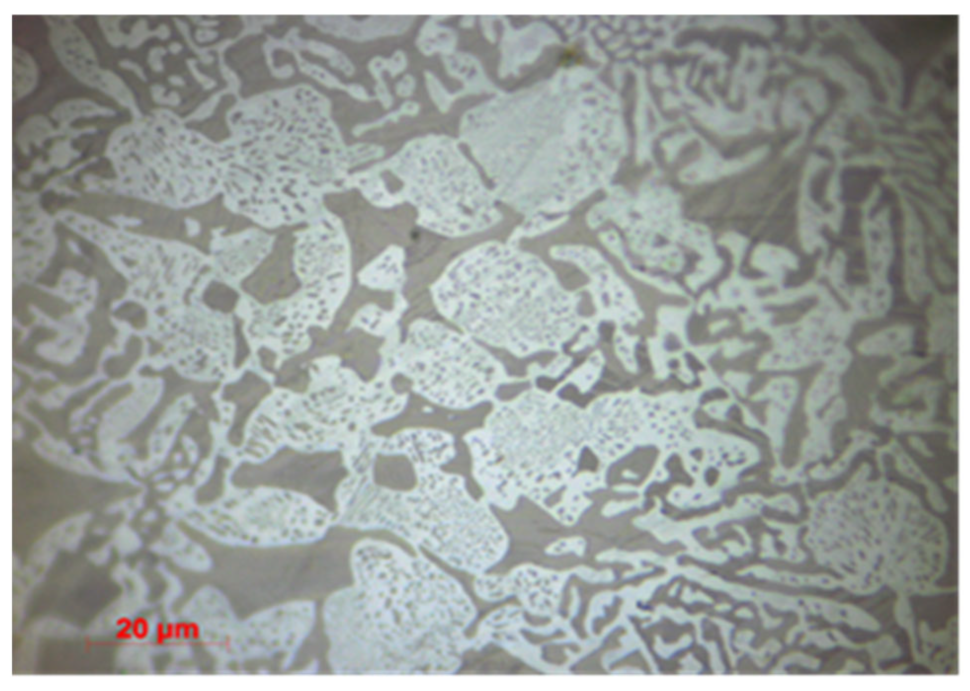
Optical (Figure 2) and SEM-BSE imaging (Figure 3) of the binary Bi60Sn40 alloy revealed a two-phase microstructure composed of Bi-rich dendrites embedded in a eutectic matrix. SEM-BSE confirmed the uniform distribution of the eutectic lamellae, while EDS mapping (Figure 4) indicated that these consisted primarily of alternating Bi- and Sn-rich phases. No additional intermetallic compounds were detected, which is consistent with expectations for a near-eutectic Bi-Sn system, corroborating earlier observations of [12].
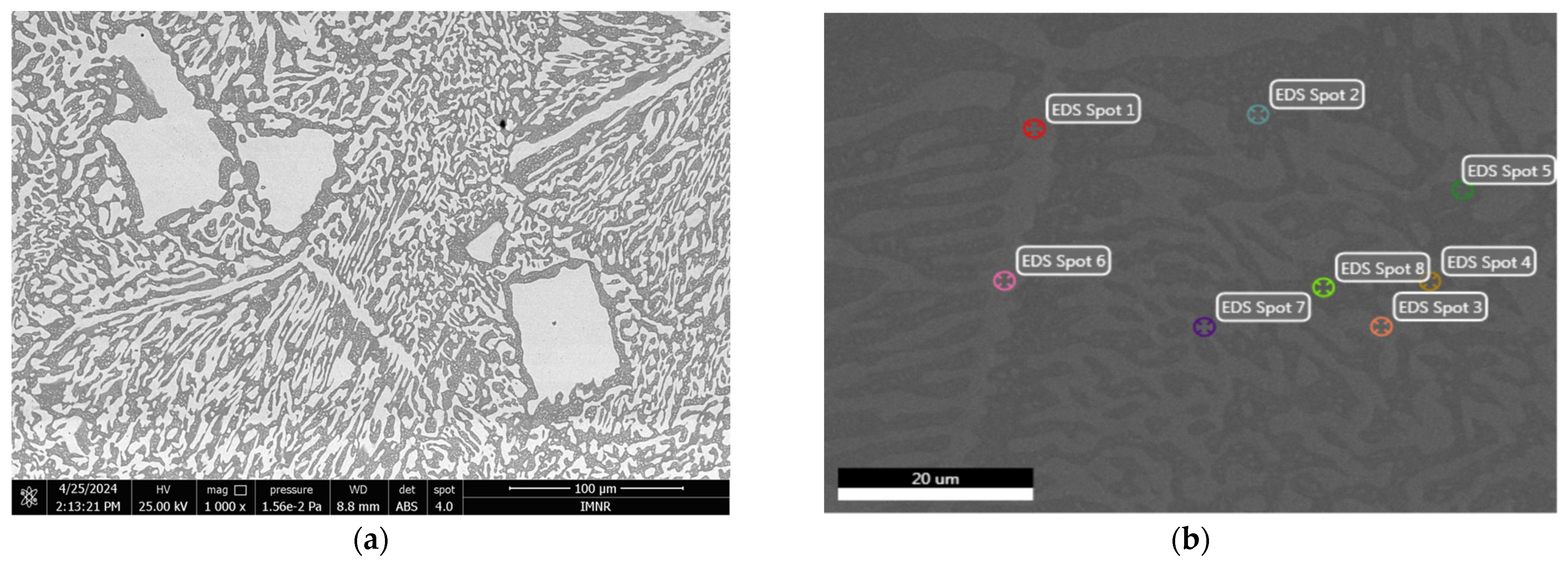
SEM micrographs of the Bi60Sn40 alloy at different magnifications are presented in Figure 3. The Bi60Sn40 alloy forms a typical eutectic microstructure, with Bi and Sn phases coexisting in a well-dispersed pattern.
Figure 3a captures finer details and shows observed lamellar spacing and phase boundaries. The light regions are likely the Bi-rich phase, while the darker ones correspond to the Sn-rich phase. The relatively uniform lamellar pattern suggests homogeneous solidification with a eutectic structure. The polygonal/rectangular islands (light gray) might be primary Bi precipitates embedded in the eutectic matrix. Figure 3b provides a broader view of the microstructural distribution and highlights the coarser eutectic pattern, with more distinct phase separation. A dendritic-like Sn-rich phase can be seen growing within a Bi-rich matrix. Table 2 presents the elemental composition of the Bi60Sn40 solder alloy obtained from different EDS point analyses.
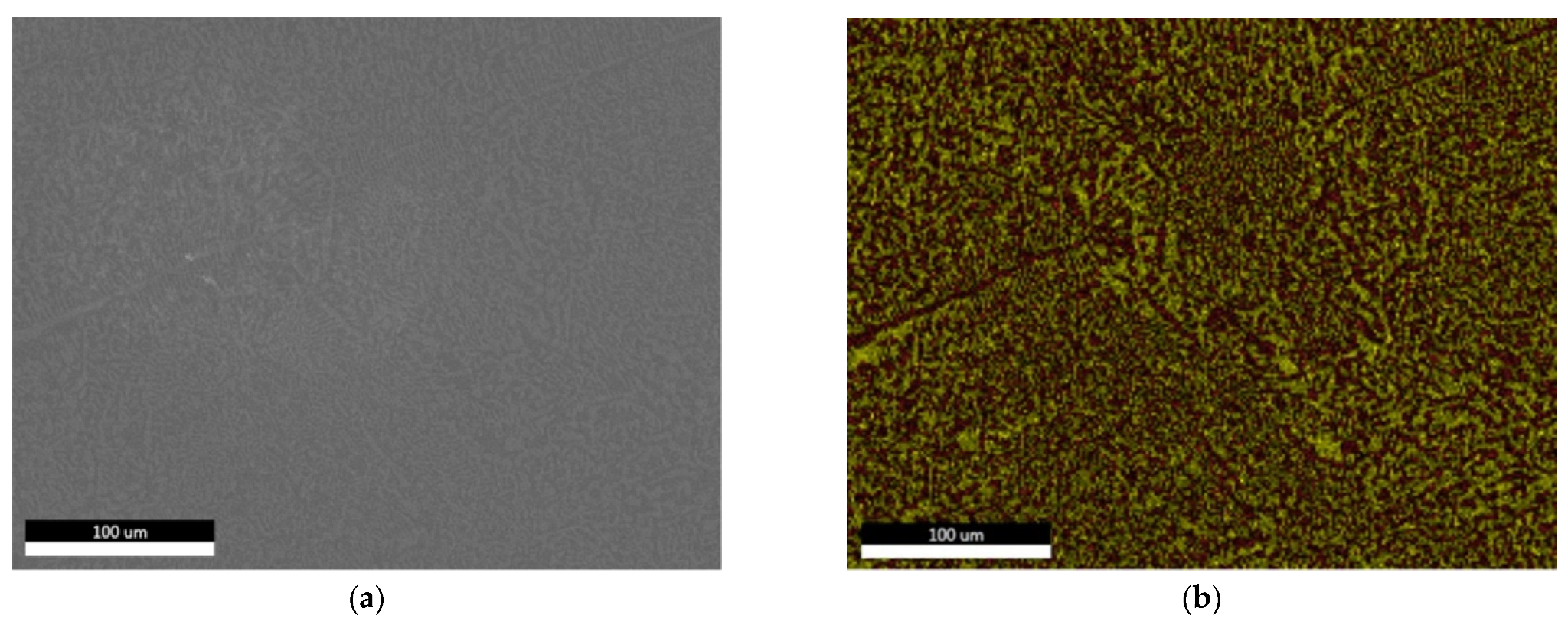
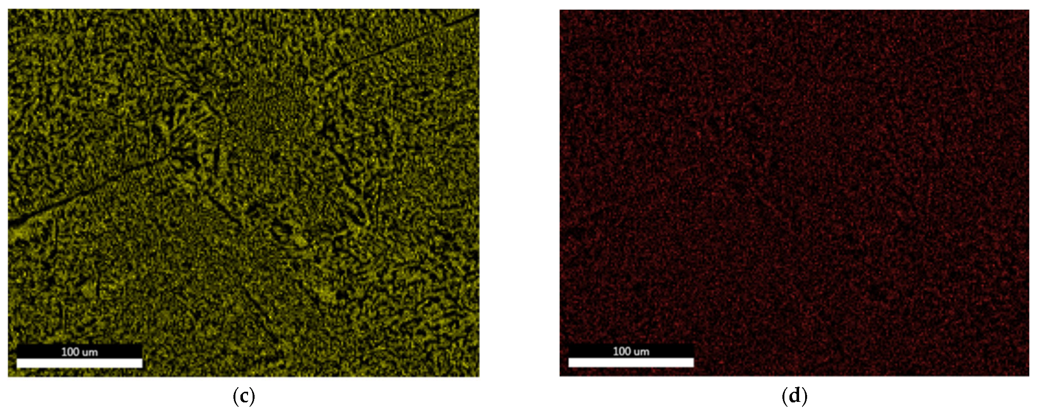
In Figure 4, the BSE imaging combined with elemental mapping via EDS was employed to visualize the distribution of the main alloying elements in the Bi60Sn40 solder alloy. Figure 4a presents the BSE microstructure, revealing compositional contrast across different phases. Figure 4b shows the superimposed elemental map with Sn in yellow and Bi in red. In Figure 4c, Sn distribution dominates, uniformly covering the matrix (yellow), which is consistent with its higher atomic percentage. Figure 4d illustrates the distribution of Bi, concentrated in smaller, dispersed regions, appearing in red. The maps indicate a heterogeneous microstructure, with Bi-rich areas embedded within a Sn-rich matrix.
Bi60Sn35Sb5 Alloy:
The Bi60Sn35Sb5 alloy displayed a more heterogeneous microstructure. Optical (Figure 5) and SEM-BSE analysis (Figure 6) showed the presence of blocky, granular secondary phases dispersed throughout the matrix. SEM-BSE imaging and EDS maps (Figure 7) confirmed Sb-rich regions co-located with Sn, suggesting the formation of SnSb-type intermetallics. Unlike the Ag-containing sample, this alloy retained larger Bi-rich areas, and the eutectic structure appeared less refined. This phase distribution corresponded to a slight reduction in thermal conductivity but retained acceptable electrical performance. In the Bi60Sn35Sb5 alloy, Sb was detected in both intermetallic (Sb2Sn3) and probable solid solution form. This dual role may contribute to the relatively heterogeneous microstructure and distinct thermophysical behavior. A study on Sn–40Bi–xSb alloys (0.1–1.0 wt% Sb) reports a hypoeutectic microstructure featuring primary Sn dendrites (~20 µm) and finer Sn–Bi eutectic lamellae (~5 µm). Notably, Sb preferentially partitions into the Sn-rich phase, with increasing Sb content introducing SnSb-type precipitates [27].
SEM micrographs of the Bi60Sn35Sb5 alloy at different magnifications are presented in Figure 6. The microstructure indicates solidification with phase segregation, common in multicomponent solder systems. The addition of 5 wt.% Sb leads to the formation of dispersed intermetallic phases, which can refine the microstructure and potentially enhance strength and thermal stability. Primary Bi structure forms first due to Bi’s high melting point, while Sn and Sb form eutectic or intermetallic structures in the residual melt.
Figure 6a shows a heterogeneous microstructure with large Bi-rich primary phases (bright gray) embedded in a matrix. Microalloying with Sb is shown to create blocky or granular SnSb intermetallic particles, especially at higher Sb levels, consistent with our SEM and EDS observations of Sb-rich secondary phases dispersed through the matrix [28]. The darker areas surrounding the Bi-rich grains are likely Sn-rich eutectic regions. Small, dispersed dark particles throughout the matrix may represent Sb-containing intermetallic or precipitates. The structure indicates partial solidification of primary Bi followed by eutectic transformation during cooling. Figure 6b displays a large primary Bi grain (bright) with a central Sb-rich particle or segregated region, possibly an intermetallic compound (dark central core). The surrounding area contains a finer distribution of small dark particles, likely Sb-based intermetallic (e.g., Bi-Sb or Sn-Sb compounds). This suggests segregation of Sb during solidification, forming discrete phases rather than a continuous solid solution. Table 3 presents the elemental composition of the Bi60Sn35Sb5 solder alloy as determined from different EDS point analysis.
Figure 7 presents BSE and EDS mapping images of the Bi60Sn35Sb5 alloy.
Figure 7a shows the BSE microstructure, highlighting compositional contrasts among different phases. In Figure 7b, the overlapped elemental map visualizes Sn (yellow), Bi (red), and Sb (green). Figure 7c reveals that Sn is predominantly distributed in the matrix, forming a continuous phase. Figure 7d shows Bi-rich regions that appear more localized and concentrated, and Figure 7e indicates a uniform but somewhat dispersed presence of Sb, primarily located around or between the Sn and Bi phases. The elemental maps confirm a heterogeneous distribution, with each element forming distinct microstructural domains.
Bi60Sn35Ag5 Alloy:
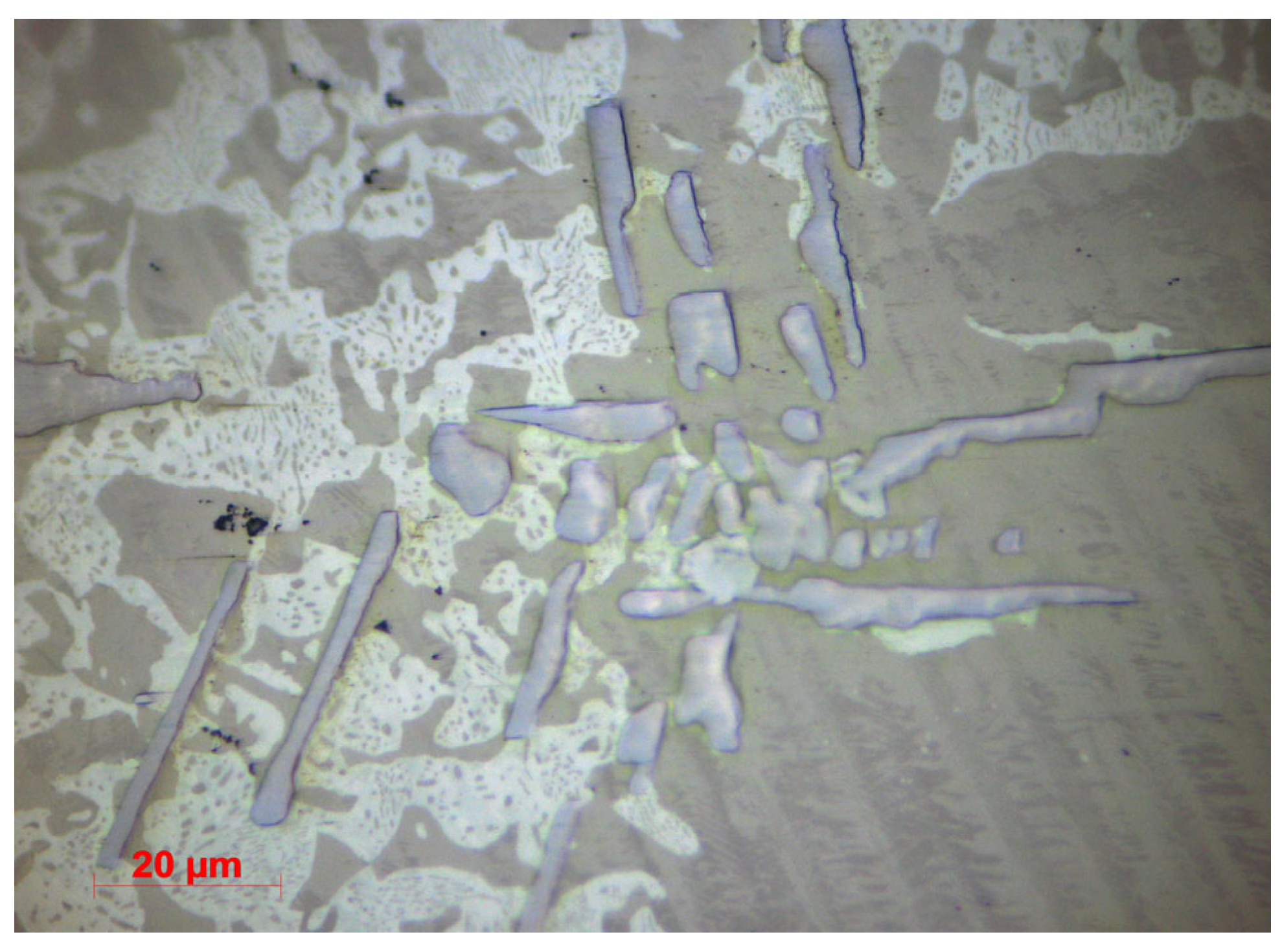
In the Bi60Sn35Ag5 alloy, the microstructure exhibited refined eutectic spacing and the emergence of secondary needle-like phases. Optical (Figure 8) and SEM-BSE analysis (Figure 9) showed these as bright, elongated features consistent with Ag3Sn intermetallics.
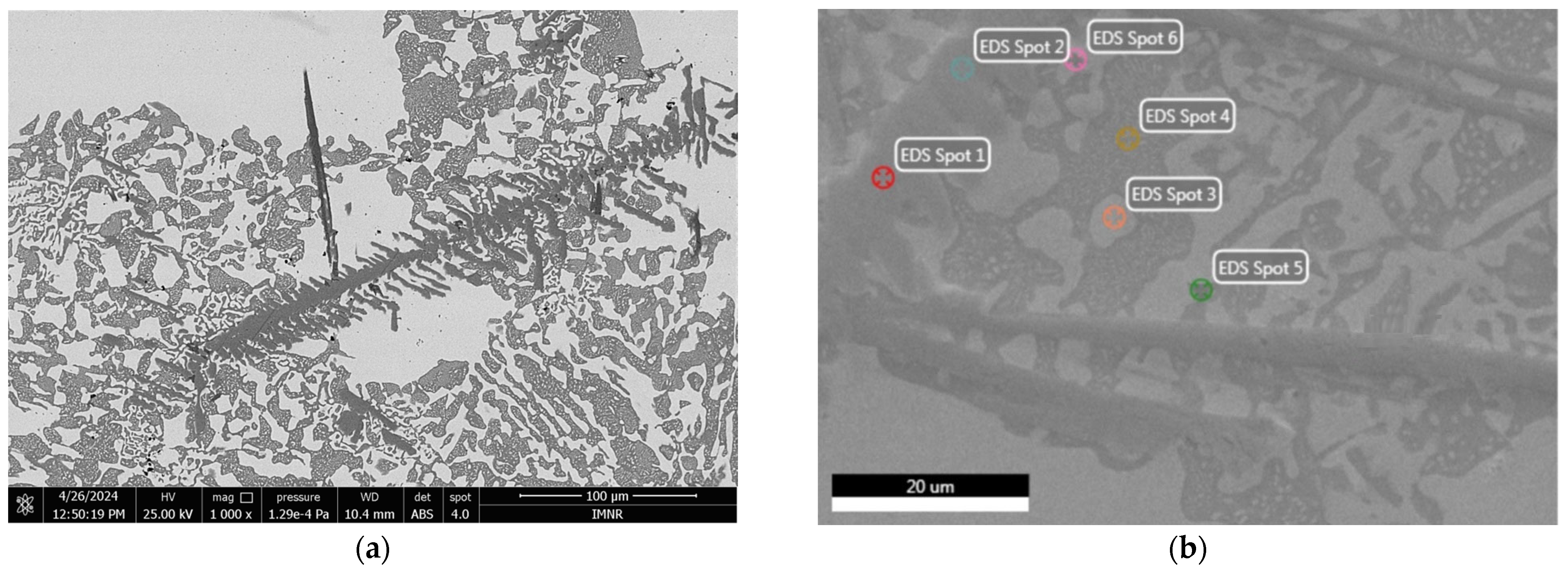
The Ag addition appeared to suppress coarse Bi-rich dendrites and promoted a finer and more interconnected eutectic structure, as reported also by [28]. Ag in Bi60Sn35Ag5 predominantly forms discrete Ag3Sn intermetallics, with no measurable solid solubility observed in either the Bi- or Sn-rich phases. These changes are correlated with improved electrical conductivity as measured by four-point probe analysis. The presence of Ag3Sn contributes to improved hardness and thermal stability, but its structure and distribution must be controlled to avoid embrittlement. The observed structure confirms that Ag addition significantly alters the microstructure by promoting intermetallic formation and refining the eutectic structure.
The SEM-BSE micrographs presented in Figure 9 correspond to the Bi60Sn35Ag5 solder alloy at different magnifications, revealing a complex multiphase microstructure. The microstructure in Figure 9a exhibits a dendritic or eutectic-like matrix, likely composed of Bi-rich and Sn-rich phases. A notable feature is the presence of elongated and interconnected intermetallic compounds (IMCs), prominently oriented along specific crystallographic directions. These IMCs are characteristic of Ag3Sn, formed due to the interaction between Ag and Sn during solidification. The uniform distribution of these phases suggests a relatively homogeneous alloy structure. Figure 9b provides a more detailed view of the IMCs, which appear as long, rod-like or needle-shaped structures embedded in the eutectic matrix. These features are consistent with Ag3Sn intermetallic, which tends to form as elongated precipitates. The surrounding matrix exhibits fine lamellar or granular structure, indicative of a eutectic reaction between Bi and Sn. The study on Sn–Ag eutectic and hypereutectic alloys (e.g., Sn–3.7 wt.% Ag up to 5.5 wt.% Ag) showing fine eutectic spacing in directionally solidified samples and the presence of elongated, needle- or plate-like Ag3Sn intermetallic compounds dispersed within the eutectic matrix [29] agrees with our observations. The formation of discrete Ag3Sn IMCs—rather than substantial Ag solid solution—aligns with the general behavior of Sn–Bi–Ag systems, where Ag primarily forms IMCs and has minimal solubility in Bi or Sn phases [30].
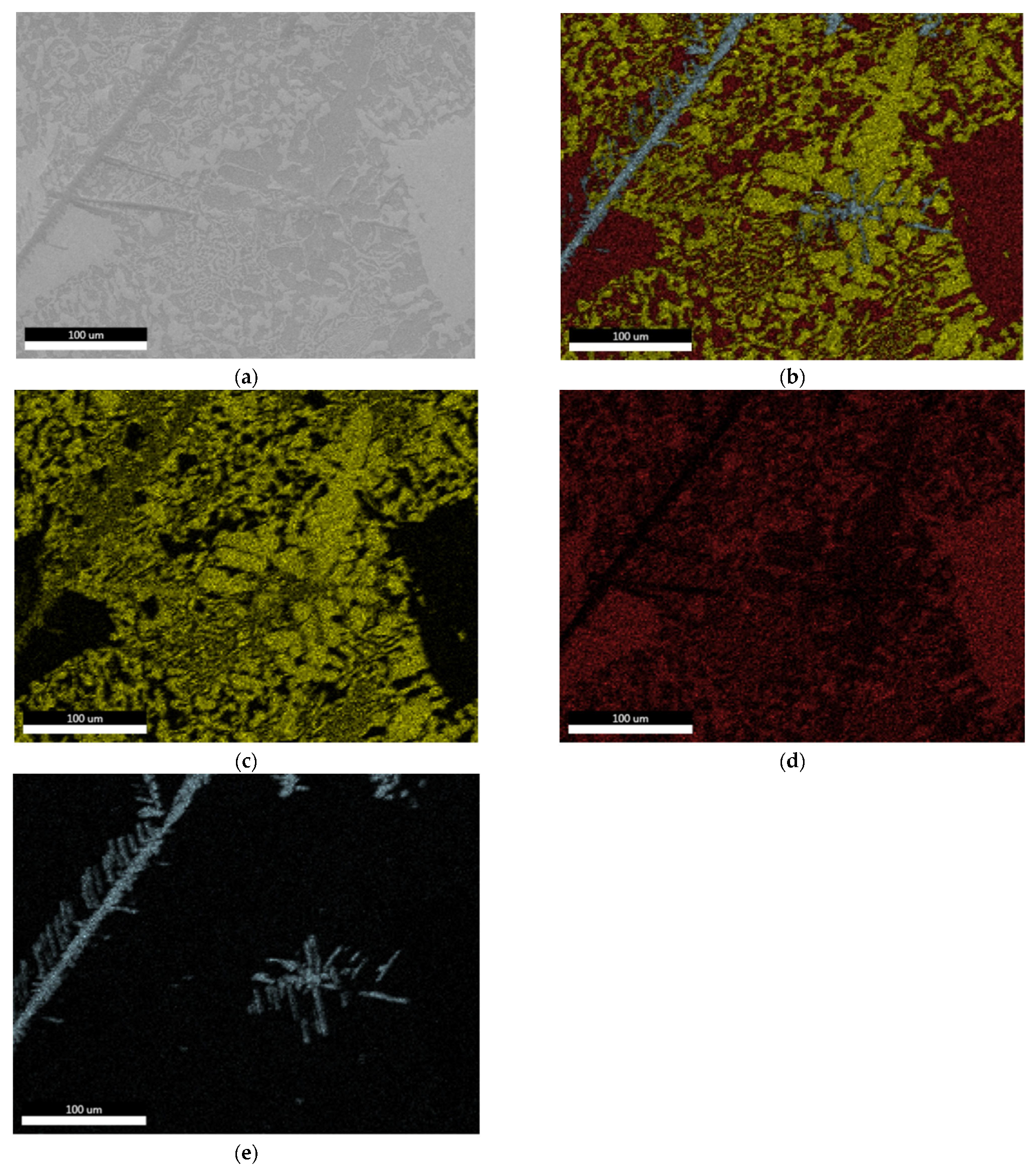
Figure 10 presents BSE and EDS mapping images of the Bi60Sn35Ag5 solder alloy. Figure 10a shows the overall BSE micrograph, where heavier elements such as Bi and Ag appear brighter due to their higher atomic numbers. Figure 10b presents the elemental distribution overlay, indicating Sn in yellow (65%), Bi in red (35%), and Ag in blue (22%). Individual maps of Sn, Bi, and Ag are displayed in Figure 10c, Figure 10d, and Figure 10e, respectively.
Table 4 presents the elemental composition of the Bi60Sn35Ag5 solder alloy obtained through different EDS point analysis. The analysis provides detailed data on the weight and atomic percentages of the main constituent elements: Sn, Ag, and Bi.
Notably, Ag appears as distinct acicular, or needle-like, precipitates aligned along phase boundaries. EDS mapping in these systems confirms Ag enrichment precisely in those elongated IMC regions. These detailed mapping aids in understanding the alloy’s phase microstructure and elemental homogeneity, which are crucial for its mechanical and thermal performance. It is important to note that the elemental concentrations reported in the EDS analyses (Table 3 and Table 4) reflect localized measurements performed on selected microstructural features, such as intermetallic compounds or phase-enriched zones. As such, these values are not directly comparable to the bulk chemical composition obtained by laser-induced spectrometry (Table 1). For instance, the high Sb content (~9.87 wt.%) in the analyzed region of the Bi60Sn35Sb5 alloy, and the high Ag content (~25.82 wt.%) in the Bi60Sn35Ag5 alloy, correspond to areas where Sb- or Ag-rich phases are concentrated—particularly Sb-based precipitates or Ag3Sn intermetallics. These local enrichments are expected and consistent with microstructural segregation during solidification. The LIBS measurements, by contrast, provide a more accurate representation of the overall alloy composition. Therefore, EDS results should be interpreted qualitatively and as a complement to bulk analysis, primarily serving to confirm elemental presence and phase identification within the solder matrix.

3.2. Microhardness Evaluation of Bi-Sn-Based Solder Alloys

Mechanical testing was beyond the scope of this study; however, the observed microstructural refinement suggests improved strength potential, so we evaluated the Vickers microhardness of the studied alloys. Table 5 presents the Vickers microhardness values measured for three Bi–Sn-based solder alloys: the binary eutectic alloy Bi60Sn40 and two ternary modifications containing 5 wt.% Sb (Bi60Sn35Sb5) and 5 wt.% Ag (Bi60Sn35Ag5), respectively.
The binary eutectic Bi60Sn40 alloy exhibits a relatively low average hardness (~14.6 HV), consistent with its soft lamellar microstructure composed of Bi-rich and β-Sn phases, as reported for near-eutectic Sn–Bi solders [31]. The addition of 5 wt% Sb increases hardness to ~16.4 HV, due to the combined effects of solid solution strengthening and formation of Sb-containing intermetallics. In contrast, the Ag-containing Bi60Sn35Ag5 alloy exhibits the highest average hardness (~17.3 HV), attributed to the dispersion of Ag3Sn particles, which effectively impede dislocation motion. These trends—Ag providing slightly greater hardening than Sb—are consistent with the established literature [32,33]. Future work will focus on tensile and creep tests to evaluate ductility and reliability.

3.3. Thermal and Electrical Conductivity of Bi-Sn-Based Solder Alloys

The thermal and electrical conductivities of the Bi60Sn40, Bi60Sn35Ag5, and Bi60Sn35Sb5 alloys were systematically evaluated to understand their thermophysical behavior across a temperature range of 25 °C to 140 °C. The results obtained are presented in Table 6. Although metals typically exhibit decreasing thermal conductivity with temperature, eutectic Bi-Sn systems may show non-monotonic behavior due to phonon–electron scattering and structural transitions. The trend observed here may also reflect measurement sensitivity to specific heat estimation.
Bi60Sn40 alloy shows the highest thermal conductivity values across the full temperature range, rising from 16.93 W/m·K at 25 °C to 26.93 W/m·K at 140 °C, likely due to its simpler binary composition with fewer scattering centers, suggesting enhanced phonon and electron transport as temperature rises. Alloys Bi60Sn35Ag5 and Bi60Sn35Sb5 exhibit a clear decline in thermal conductivity with increasing temperature, a typical behavior at elevated temperatures. The addition of Ag slightly reduced λ in Bi60Sn35Ag5, starting from 18.28 W/m·K to 16.77 W/m·K at 140 °C, indicating that silver addition may introduce scattering centers or phase boundaries that hinder heat conduction.
In contrast, Bi60Sn35Sb5 exhibited the lowest λ, decreasing from 13.90 W/m·K to 10.66 W/m·K, indicating that Sb impairs thermal transport more significantly, likely due to its effect on phonon scattering and microstructural complexity. Electrical resistivity increases with temperature across all alloys, consistent with the classical metallic behavior where lattice vibrations impede electron flow at higher temperatures.
The binary Bi60Sn40 alloy exhibits an atypical increase in thermal conductivity with rising temperature. This contrasts with the expected metallic trend observed in both ternary alloys, where thermal conductivity decreases due to enhanced phonon scattering and reduced carrier mobility. We believe that this anomalous behavior in the binary alloy may be related to the absence of complex intermetallic compounds (e.g., Ag3Sn or Sb2Sn3), which otherwise scatter electrons and phonons more effectively, and/or a possible thermally activated reordering of the eutectic structure or reduction in interface resistance at moderate temperatures, enhancing thermal transport. Bi60Sn40 exhibits increasing electrical resistivity from 3.80·10−7 Ω·m to 8.35·10−7 Ω·m, and a corresponding decrease in conductivity from 2.63·106 S/m to 1.20·106 S/m as temperature increases—expected behavior due to enhanced phonon scattering. Bi60Sn35Ag5 starts with a very low resistivity (1.52·10−7 Ω·m) and high electrical conductivity (6.54·106 S/m) at 25 °C. Although σ decreases slightly with temperature, it remains the highest among all alloys, indicating that Ag significantly enhances electrical transport. Bi60Sn35Sb5 shows similar electrical performance to the Ag-containing alloy at 25 °C, with σ = 6.52·106 S/m, but its conductivity decreases more significantly with temperature, reaching 4.79·106 S/m at 140 °C. This suggests that Sb has a moderately positive impact on σ at low temperatures, but less thermal stability than Ag.
The standard deviation (s) values for the three solder alloys indicate differences in their thermal and electrical behavior. The Bi60Sn40 alloy exhibits a high standard deviation (s = 3.74), suggesting significant variability and a high sensitivity to temperature fluctuations. This implies less consistent performance under changing thermal conditions. In contrast, the Bi60Sn35Ag5 alloy shows a low standard deviation (s = 0.64), indicating low variability and suggesting stable conductivity and reliable performance. The addition of silver appears to enhance the stability of the alloy. The Bi60Sn35Sb5 alloy displays a moderate standard deviation (s = 1.37), representing an intermediate level of variability. This suggests a balance between performance stability and sensitivity, making it potentially suitable for applications that tolerate some fluctuation.
The data demonstrates that alloying with Ag or Sb enhances electrical conductivity significantly compared to the base Bi60Sn40 alloy. However, Ag provides a better balance between thermal and electrical performance, while Sb tends to degrade thermal conductivity more sharply. These combined thermal and electrical characterizations highlight the significant impact of alloying elements on the solder alloys’ performance, providing critical data for optimizing low-temperature soldering processes in electronic applications.

4. Conclusions

Bi-Sn-based solder alloys, particularly those modified with small additions of Sb or Ag, represent a strong class of lead-free alternatives, offering a balance between environmental safety and high-performance requirements. SEM and BSE imaging revealed the emergence of new intermetallic phases in the ternary alloys, while EDS analysis confirmed a uniform elemental distribution in the base Bi60Sn40 alloy and localized enrichment of Sb and Ag in modified systems. These microstructural shifts suggest that minor alloying additions can effectively tailor phase formation and improve functional performance.
The results confirm that both Ag and Sb additions significantly alter the microstructure and thermophysical properties of Bi-Sn alloys:
  • Sb induces granular Sn-Sb intermetallics that may strengthen the structure but degrade thermal transport;
  • Ag promotes fine, directional intermetallics (Ag3Sn), enhances electrical conductivity, and moderately reduces thermal conductivity;
  • Both Ag and Sb raise electrical conductivity compared to the binary alloy, reflecting complex structural interactions;
  • The binary Bi60Sn40 serves as a stable baseline, offering high thermal conductivity and a uniform eutectic structure suitable for low-temperature soldering.
A clear trade-off between thermal and electrical performance was observed:
  • Ag increases electrical conductivity but slightly lowers thermal conductivity at higher temperatures.
Although the current study focused primarily on microstructural and thermophysical characterization, we acknowledge the critical importance of mechanical performance for solder alloy applications. Preliminary metallographic observations and microhardness testing suggest that the addition of Ag and Sb improves strength via intermetallic formation and microstructural refinement. The binary eutectic Bi60Sn40 has a low average hardness, but with Sb addition, it increases to 16.36 HV. Ag-containing alloys have the highest average hardness (17.33 HV), with Ag having a slightly greater hardening effect.
Future work will include quantitative evaluation of tensile strength and creep resistance for these alloys to establish comprehensive structure–property-performance relationships and validate their suitability for demanding electronic packaging environments. In addition to the proposed avenues for further research, it is essential to repeat similar microstructural and thermophysical studies using realistic reflow profiles and processing temperatures closer to the alloys’ respective liquidus points. Since the current specimens were fabricated at significantly higher temperatures to ensure homogenization, such experiments will be critical to verify whether the observed trends in phase formation, thermal conductivity, and electrical conductivity are representative of real-world soldering conditions.

Author Contributions

Conceptualization, A.-A.I., F.N. and G.I.;dData curation, A.-A.I., F.N., G.I. and I.P.; formal analysis, A.-A.I., F.N., G.I., I.P., F.M., R.B., D.-V.D., A.-C.M., M.G., A.P. and C.U.; funding acquisition, A.-A.I. and R.B.; investigation, F.N., G.I., I.P., F.M., D.-V.D., A.-C.M., M.G., A.P. and C.U.; methodology, F.N., G.I., I.P. and F.M.; project administration, F.N. and G.I.; resources, A.-A.I., F.N., G.I. and R.B.; software, A.-A.I., F.N., G.I., I.P., F.M., R.B., D.-V.D., A.-C.M., M.G., A.P. and C.U.; supervision, F.N. and G.I.; validation, F.N. and G.I.; visualization, A.-A.I., F.N. and G.I.; writing—original draft, A.-A.I., F.N. and G.I.; writing—review and editing, F.N., G.I. and I.P. All authors have read and agreed to the published version of the manuscript.

Funding

This research received no external funding.

Institutional Review Board Statement

Not applicable.

Informed Consent Statement

Not applicable.

Data Availability Statement

The original contributions presented in this study are included in the article. Further inquiries can be directed to the corresponding authors.

Conflicts of Interest

The authors declare no conflicts of interest.

References

  1. Vianco, P.T.; Rejent, J.A. Properties of ternary Sn-Ag-Bi solder alloys: Part I—Thermal properties and microstructural analysis. J. Electron. Mater. 1999, 28, 1127–1137. [Google Scholar] [CrossRef]
  2. Abtew, M.; Selvaduray, G. Lead-free Solders in Microelectronics. Mater. Sci. Eng. R. Rep. 2000, 27, 95–141. [Google Scholar] [CrossRef]
  3. Shen, Y.A.; Chen, F.Y.; Gao, R.; Ho, C.E.; Nishikawa, H.; Chen, C.M. Effect of Bi Addition on Melting Behavior, Solder Joint Strength, and Thermal Aging Resistance of Sn-3.5Ag/Cu Joints. JOM 2025, 77, 4206–4214. [Google Scholar] [CrossRef]
  4. EEA—European Environment Agency. Available online: https://www.eea.europa.eu/en/european-zero-pollution-dashboards/indicators/progress-in-regulating-lead-signal (accessed on 12 June 2025).
  5. Razak, N.R.A.; Salleh, M.A.A.M.; Saud, N.; Said, R.M.; Ramli, M.I.I. Influence of Bismuth in Sn-Based Lead-Free Solder—A Short Review. Solid State Phenom. 2018, 273, 40–45. [Google Scholar] [CrossRef]
  6. Koleňák, R.; Provazník, M.; Kostolný, I.; Kar, A. Soldering by the Active Lead-Free Tin and Bismuth-Based Solders. In Lead Free Solders; Kar, A., Ed.; IntechOpen: Rijeka, Croatia, 2018. [Google Scholar] [CrossRef]
  7. Kattner, U. NIST Phase Diagrams and Computational Thermodynamics—Solder Systems—SRD 139, National Institute of Standards and Technology; 1990. Available online: https://www.metallurgy.nist.gov/phase/solder/bisn.html (accessed on 2 August 2025).
  8. Kang, H.; Rajendran, S.H.; Jung, J.P. Low Melting Temperature Sn-Bi Solder: Effect of Alloying and Nanoparticle Addition on the Microstructural, Thermal, Interfacial Bonding, and Mechanical Characteristics. Metals 2021, 11, 364. [Google Scholar] [CrossRef]
  9. Hashim, M.S.; Osman, S.A.; Efzan, E. The Development of Low-Temperature Lead-Free Solders using Sn-Bi Solders Alloys. Int. J. Recent Technol. Eng. 2019, 8, 11956–11962. [Google Scholar] [CrossRef]
  10. Ren, G.; Collins, M.N. Improved Reliability and Mechanical Performance of Ag Microalloyed Sn58Bi Solder Alloys. Metals 2019, 9, 462. [Google Scholar] [CrossRef]
  11. Shen, Y.A. Influence of Ag and Zn on the Microstructure and Properties of Sn-40 Bi Alloy for Improved Soldering Applications. ACS Appl. Electron. Mater. 2024, 6, 8084–8093. [Google Scholar] [CrossRef]
  12. Silva, B.L.; Reinhart, G.; Nguyen-Thi, H.; Mangelinck-Noël, N.; Garcia, A.; Spinelli, J.E. Microstructural development and mechanical properties of a near-eutectic directionally solidified Sn–Bi solder alloy. Mater. Charact. 2015, 107, 43–53. [Google Scholar] [CrossRef]
  13. Zhang, P.; Xue, S.; Liu, L.; Wang, J.; Tatsumi, H.; Nishikawa, H. Influence of Isothermal Aging on Microstructure and Shear Property of Novel Epoxy Composite SAC305 Solder Joints. Polymers 2023, 15, 4168. [Google Scholar] [CrossRef]
  14. Kang, J.; Sharma, A.; Jung, J.P. Low-melting and thermal-conducting Sn-Bi-Ag solder enhanced with SnO2 nanoparticles for reliable mini-LED microsystems. J. Mater. Sci. Mater. Electron. 2025, 36, 693. [Google Scholar] [CrossRef]
  15. Novikov, A.; Nowottnick, M. Composite Soldering Materials Based on BiSnAg for High-Temperature Stable Solder Joints. J. Microelectron. Packag. 2022, 19, 115–122. [Google Scholar] [CrossRef]
  16. Bhavan, J.S.; Pazhani, A.; Amer, M.; Patel, N.; Tg, U. Microstructural Evolution and Phase Transformation on Sn–Ag Solder Alloys under High-Temperature Conditions Focusing on Ag3Sn Phase. Adv. Eng. Mater. 2024, 26, 2400660. [Google Scholar] [CrossRef]
  17. Bhavan, J.S.; Kadavath, G.; Honecker, D.; Pazhani, A. Small-angle neutron scattering analysis in Sn-Ag Lead-free solder alloys: A focus on the Ag3Sn intermetallic phase. Mater. Charact. 2024, 217, 114385. [Google Scholar] [CrossRef]
  18. Kim, Y.S.; Kim, K.S.; Hwang, C.W.; Suganuma, K. Effect of composition and cooling rate on microstructure and tensile properties of Sn–Zn–Bi alloys. J. Alloys Compd. 2003, 352, 237–245. [Google Scholar] [CrossRef]
  19. Liu, Y.; Tu, K.N. Low melting point solders based on Sn, Bi, and In elements. Mater. Today Adv. 2020, 8, 100115. [Google Scholar] [CrossRef]
  20. Zhou, J.; Tan, X.F.; McDonald, S.D.; Nogita, K. Phase Transformations and Mechanical Properties in In–Bi–Sn Alloys as a Result of Low-Temperature Storage. Materials 2024, 17, 3669. [Google Scholar] [CrossRef] [PubMed]
  21. Yeo, S.M.; Yow, H.K.; Yeoh, K.H. Lead-Free BiSnAg Soldering Process for Voidless Semiconductor Packaging. IEEE Trans. Compon. Packag. Manuf. Technol. 2023, 13, 1310–1315. [Google Scholar] [CrossRef]
  22. Zhang, L.; Xue, S.B.; Gao, L.L.; Sheng, Z.; Ye, H.; Xiao, Z.X.; Zeng, G.; Chen, Y.; Yu, S.L. Development of Sn–Zn lead-free solders bearing alloying elements. J. Mater. Sci. Mater. Electron. 2009, 21, 1–15. [Google Scholar] [CrossRef]
  23. Wu, X.; Hou, Z.; Xie, X.; Lin, P.; Huo, Y.; Wang, Y.; Zhao, X. Mechanical properties and microstructure evolution of Sn–Bi-based solder joints by microalloying regulation mechanism. J. Mater. Res. Technol. 2024, 31, 3226–3237. [Google Scholar] [CrossRef]
  24. Zhou, J.; Tan, X.F.; McDonald, S.D.; Nogita, K. Mechanical Properties and Microstructure of Binary In-Sn Alloys for Flexible Low Temperature Electronic Joints. Materials 2022, 15, 8321. [Google Scholar] [CrossRef]
  25. Leal, J.R.d.S.; Reyes, R.A.V.; Gouveia, G.L.d.; Coury, F.G.; Spinelli, J.E. Evaluation of Solidification and Interfacial Reaction of Sn-Bi and Sn-Bi-In Solder Alloys in Copper and Nickel Interfaces. Metals 2024, 14, 963. [Google Scholar] [CrossRef]
  26. Iacob, G.; Ghica, V.G.; Petrescu, M.I.; Niculescu, F.; Butu, M.; Stancel, C.D.; Stanescu, M.M.; Ilie, A.A. Research on the development and characterization of Bi-Sn, Bi-Sn-Sb and Bi-Sn-Ag solder alloys. UPB Sci. Bull. B Chem. Mater. Sci. 2024, 86, 187–198. [Google Scholar]
  27. Yamauchi, A.; Kurose, M. Effect of Sb and Zn Addition on the Microstructures and Tensile Properties of Sn-Bi-Based Alloys. Materials 2022, 15, 884. [Google Scholar] [CrossRef] [PubMed]
  28. Fowler, H.N.; Tay, S.X.; Blendell, J.; Handwerker, C.A. Microalloying effects of Sb and Ag on the microstructural evolution of eutectic Sn–Bi alloys. MRS Adv. 2023, 8, 763–767. [Google Scholar] [CrossRef]
  29. Hou, N.; Xian, J.W.; Sugiyama, A.; Yasuda, H.; Gourlay, C.M. Ag3Sn Morphology Transitions During Eutectic Growth in Sn–Ag Alloys. Met. Mater. Trans. A 2023, 54, 909–927. [Google Scholar] [CrossRef]
  30. Šebo, P.; Švec, P.; Janičkovič, D.; Illeková, E.; Zemánková, M.; Sidorov, V.; Švec, P.; Plevachuk, Y. The influence of silver content on structure and properties of Sn–Bi–Ag solder and Cu/solder/Cu joints. Mater. Sci. Eng. A 2013, 571, 184–192. [Google Scholar] [CrossRef]
  31. Shen, L.; Septiwerdani, P.; Chen, Z. Elastic modulus, hardness and creep performance of SnBi alloys using nanoindentation. Mater. Sci. Eng. A 2012, 558, 253–258. [Google Scholar] [CrossRef]
  32. Yang, T.; Chen, Y.; You, K.; Dong, Z.; Jia, Y.; Wang, G.; Peng, J.; Cai, S.; Luo, X.; Liu, C.; et al. Effect of Bi, Sb, and Ti on Microstructure and Mechanical Properties of SAC105 Alloys. Materials 2022, 15, 4727. [Google Scholar] [CrossRef]
  33. Fathy, N. Interfacial Microstructure and Shear Strength Improvements of Babbitt–Steel Bimetal Composites Using Sn–Bi Interlayer via Liquid–Solid Casting. Sustainability 2023, 15, 804. [Google Scholar] [CrossRef]
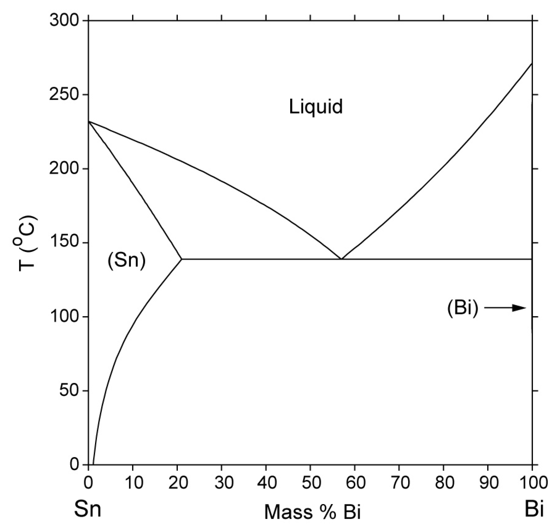
Figure 1. Phase diagram of Bi-Sn system. Reprinted with permission from ref. [7].
Metals 15 00915 g001
Figure 2. Optical micrograph of Bi60Sn40 alloy showing fine dendritic structure, with randomly oriented dendrites trapped in a eutectic matrix.
Metals 15 00915 g002
Figure 3. SEM micrographs of the Bi60Sn40 alloy: (a) Fine eutectic lamellar structure consisting of alternating Bi-rich (bright) and Sn-rich (dark) phases, with occasional primary Bi particles visible as larger polygonal regions (magnification: 1000×); (b) Coarser eutectic structure showing directional growth and partial dendritic structures, indicating the EDS analysis points (magnification: 5000×).
Metals 15 00915 g003
Figure 4. BSE and elemental mapping images of the Bi60Sn40 solder alloy: (a) BSE micrograph; (b) combined elemental map (Sn—yellow, Bi—red); (c) Sn distribution (65%); (d) Bi distribution (35%). The microstructure reveals a Sn-rich matrix with dispersed Bi-rich regions.
Metals 15 00915 g004aMetals 15 00915 g004b
Figure 5. Optical micrograph of Bi60Sn35Sb5 alloy showing eutectic phase and phase boundaries with primary, Bi, and spheroidal, Sn-Sb, compounds.
Metals 15 00915 g005
Figure 6. SEM micrographs of the Bi60Sn35Sb5 alloy: (a) Microstructure with large primary Bi-rich grains embedded in a Sn-rich eutectic matrix and dispersed Sb-containing precipitates (magnification: 1000×); (b) Enlarged view of a primary Bi grain containing a central Sb-rich inclusion and surrounding fine intermetallic dispersions with the EDS analysis points (magnification: 5000×).
Metals 15 00915 g006
Figure 7. BSE and elemental mapping images of the Bi60Sn35Sb5 solder alloy: (a) BSE micrograph; (b) combined elemental map (Sn—yellow, Bi—red, Sb—green); (c) Sn distribution (41%); (d) Bi distribution (34%); (e) Sb distribution (22%). The microstructure shows clear phase separation with Sn-rich, Bi-rich, and Sb-containing regions.
Metals 15 00915 g007
Figure 8. Optical micrograph of Bi60Sn35Ag5 alloy showing complex dendritic structure with presence of dispersed Ag inclusions, with a lamellar–globular structure.
Metals 15 00915 g008
Figure 9. SEM micrographs of the Bi60Sn35Ag5 solder alloy: (a) General microstructure showing Bi–Sn eutectic regions and elongated intermetallic compounds (magnification: 1000×); (b) Higher magnification image highlighting needle-like Ag3Sn intermetallic phases embedded in the eutectic matrix, and the EDS analysis points (magnification: 5000×).
Metals 15 00915 g009
Figure 10. BSE image and EDS elemental mapping of the Bi60Sn35Ag5 alloy: (a) BSE micrograph; (b) combined EDS map showing Sn (yellow), Bi (red), and Ag (blue); (c) Sn distribution (65%); (d) Bi distribution (35%); (e) Ag distribution (22%). Ag-rich acicular structures are visible along the phase boundaries.
Metals 15 00915 g010
Table 1. Chemical composition of the Bi-Sn-Based Solder Alloys.
Chemical Composition (%)
ElementBi60Sn40Bi60Sn35Sb5Bi60Sn35Ag5
Bi59.43759.41158.804
Sn39.47534.53334.271
Sb0.01674.880.0177
Ag004.93
Cu0.1220.1821.63
Fe0.0180.0290.024
O.E. *rem.rem.rem.
Total100100100
* O.E.–other elements (Aluminum (Al), Carbon (C), Lead (Pb), Silicon (Si), Zirconium (Zr), Zinc (Zn)).
Table 2. Elemental composition of the Bi60Sn40 solder alloy determined by EDS analysis.
EDS AnalysisElementWeight %Atomic %Net Int.Error %Peak-to-Background (P/B) Ratio Resolution,
R
Fluorescence, F
Spot 1BiL100.00100.00349.3812.34205.54121.12561.0445
Spot 2SnL31.5144.75411.537.86167.63771.05751.0067
BiL68.4955.25280.0712.92182.95321.11441.0457
Spot 3SnL2.313.9918.9345.629.96651.06281.0074
BiL97.6996.01353.4213.37200.53321.12481.0446
Spot 4SnL82.1989.041038.786.83317.07751.04791.0056
BiL17.8110.9644.8532.7838.66401.09521.0527
Spot 5SnL70.2680.62999.996.77341.44991.05021.0058
BiL29.7419.3889.6821.6078.94561.09991.0501
Spot 6SnL2.153.7214.4256.018.69001.06281.0074
BiL97.8596.28342.7111.76188.37821.12481.0446
Spot 7SnL7.6312.6982.1017.4935.34321.06181.0072
BiL92.3787.31368.2113.08205.45121.12291.0447
Spot 8SnL82.2089.051386.516.45414.24161.04791.0056
BiL17.8010.9553.7333.5550.50401.09521.0527
Table 3. Elemental composition of the Bi60Sn35Sb5 solder alloy determined by EDS analysis.
EDS AnalysisElementWeight %Atomic %Net Int.Error %Peak-to-Background (P/B) Ratio Resolution,
R
Fluorescence, F
Spot 1SnL2.744.7314.7541.7711.33631.06271.0074
BiL97.2695.27436.8311.37191.42221.12461.0446
Spot 2SnL20.2029.05371.868.01101.15521.05781.0071
SbL9.8713.84185.1911.5849.33741.06011.0073
BiL69.9357.12351.9013.20175.29691.11501.0456
Spot 3SnL19.9927.99329.998.7397.16211.05701.0072
SbL14.6720.04235.1011.4871.21881.05931.0072
BiL65.3451.97291.3613.36160.37601.11341.0458
Spot 4SnL49.8753.12966.446.79263.73301.04691.0074
SbL38.1639.63701.727.45202.04031.04881.0060
BiL11.977.2443.9339.8736.04461.09341.0538
Table 4. Elemental composition of the Bi60Sn35Ag5 solder alloy determined by EDS analysis.
EDS AnalysisElementWeight %Atomic %Net Int.Error %Peak-to-Background (P/B) Ratio Resolution,
R
Fluorescence, F
Spot 1AgL72.1874.061356.907.08332.89651.03761.0065
SnL27.8225.94328.8010.20125.17401.04291.0036
Spot 2AgL68.0971.901394.176.89329.15661.03881.0063
SnL25.8224.78340.739.98121.49511.04431.0038
BiL6.093.3211.1963.3716.65751.08801.0600
Spot 3BiL100.00100.00385.3712.23182.39311.12561.0445
Spot 4SnL74.2483.541141.596.40341.73861.04941.0057
BiL25.7616.4687.9624.1365.61651.09831.0509
Spot 5SnL46.2741.83719.746.34217.56421.04651.0076
CuK26.0343.95490.318.35155.47251.08061.1170
BiL27.6914.2295.1321.3872.20141.09261.0415
Spot 6SnL60.0647.82870.316.21271.50371.04141.0078
CuK32.9749.03605.536.40190.40631.07171.0779
BiL6.973.1512.2765.6118.47961.08231.0416
Table 5. Vickers microhardness (HV15) of Bi-Sn-based solder alloys. Values represent the mean ± standard deviation from six indentations per sample.
AlloysMicrohardness HV15 (Mean ± SD)
Bi60Sn4014.59 ± 1.69
Bi60Sn35Sb516.36 ± 3.42
Bi60Sn35Ag517.33 ± 2.79
Table 6. Thermal and electrical conductivity data of the solder alloys between 25 °C and 140 °C. Values of λ are reported as mean λ ¯ ± standard deviation (s) over the measured temperature range.
Solder AlloyTemperature
(°C)
Thermal Diffusivity
α (m2/s)
Thermal Conductivity
λ (W/m·K)
Resistivity
ρₑ (Ω·m)
Electrical Conductivity
σ (S/m)
Bi60Sn402510.75·10−616.933.80·10−72.63·106
5011.85·10−618.944.45·10−72.25·106
7512.90·10−620.935.10·10−71.96·106
10013.93·10−622.936.35·10−71.57·106
12514.93·10−624.937.60·10−71.32·106
14016.06·10−626.938.35·10−71.20·106
λ ¯ ± s = 21.93 ± 3.74
Bi60Sn35Sb5259.71·10−613.901.53·10−76.52·106
509.11·10−613.591.63·10−76.12·106
758.66·10−613.431.76·10−75.67·106
1007.23·10−611.651.88·10−75.30·106
1256.81·10−611.382.00·10−74.86·106
1406.22·10−610.662.08·10−74.79·106
λ ¯ ± s = 12.44 ± 1.37
Bi60Sn35Ag52511.91·10−618.281.52·10−76.54·106
5011.56·10−618.251.66·10−76.15·106
7510.80·10−617.521.77·10−75.69·106
10010.46·10−617.431.89·10−75.33·106
1259.89·10−616.912.01·10−74.98·106
1409.56·10−616.772.08·10−74.81·106
λ ¯ ± s = 17.53 ± 0.64
Disclaimer/Publisher’s Note: The statements, opinions and data contained in all publications are solely those of the individual author(s) and contributor(s) and not of MDPI and/or the editor(s). MDPI and/or the editor(s) disclaim responsibility for any injury to people or property resulting from any ideas, methods, instructions or products referred to in the content.