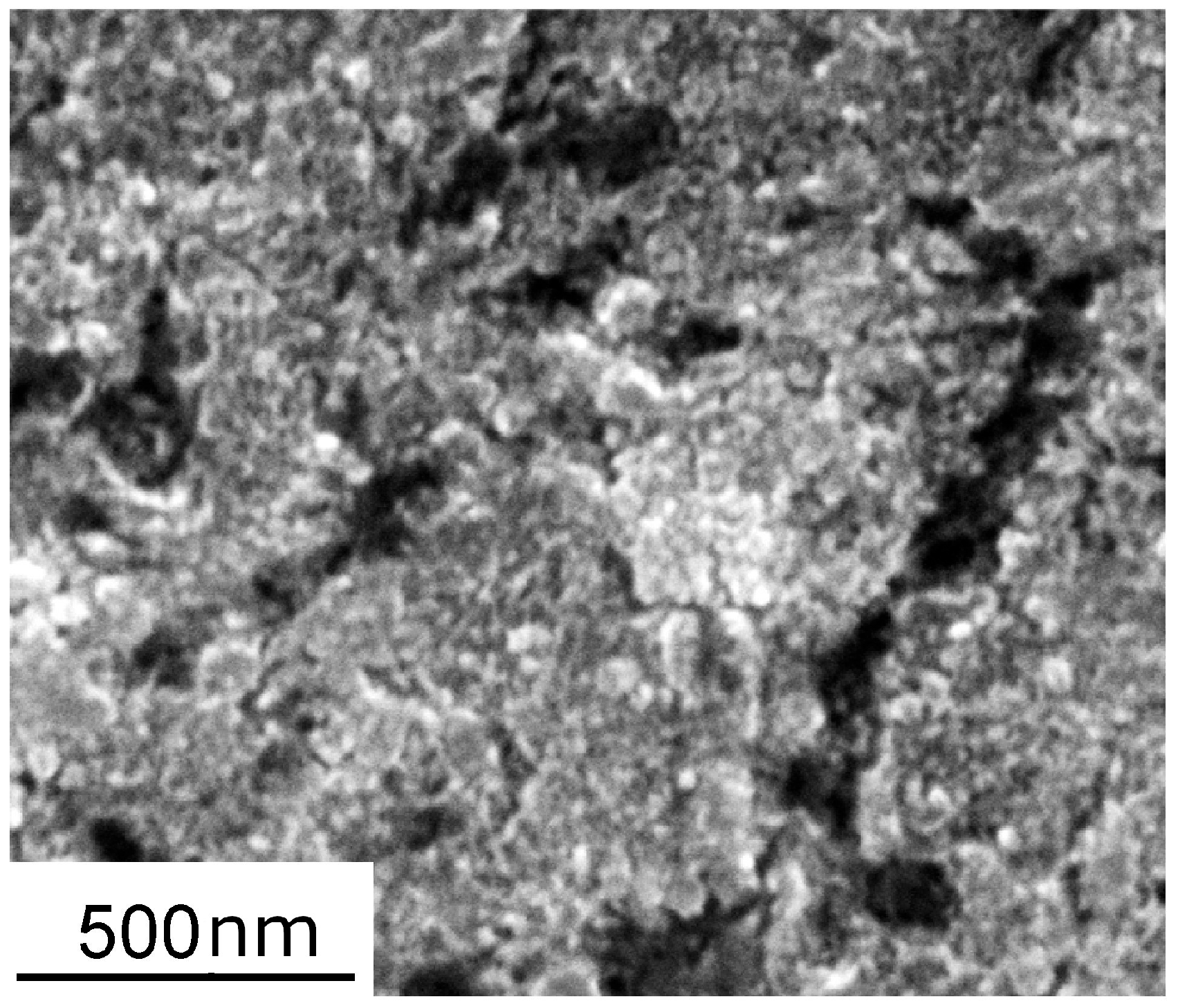
Figure 1.
Secondary electron image of anodized AlSi10Mg surface.
Figure 2.
Laser scan patterns.
Figure 3.
Secondary electron micrographs of the deep-etched AlSi10Mg LBPF sample.
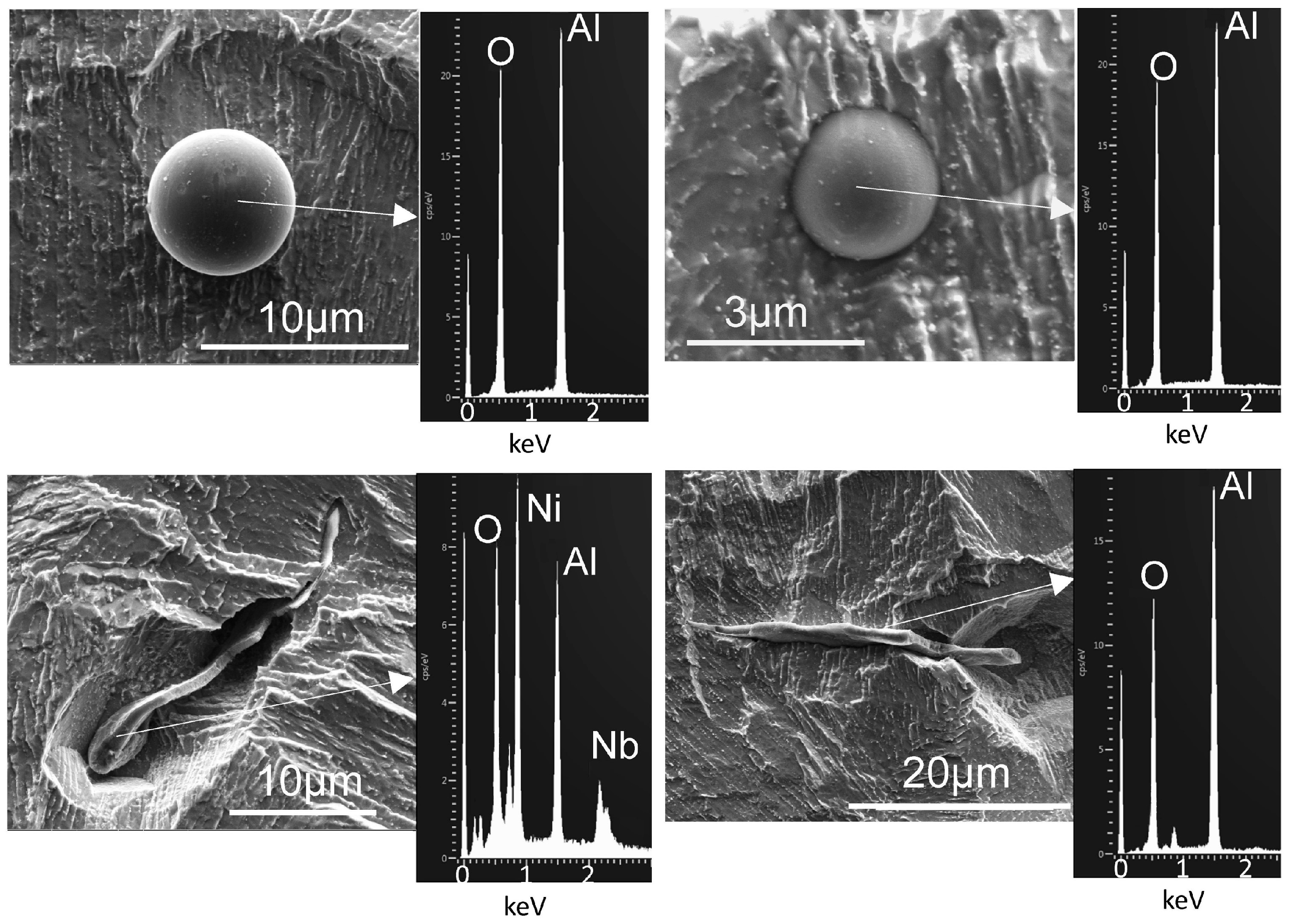
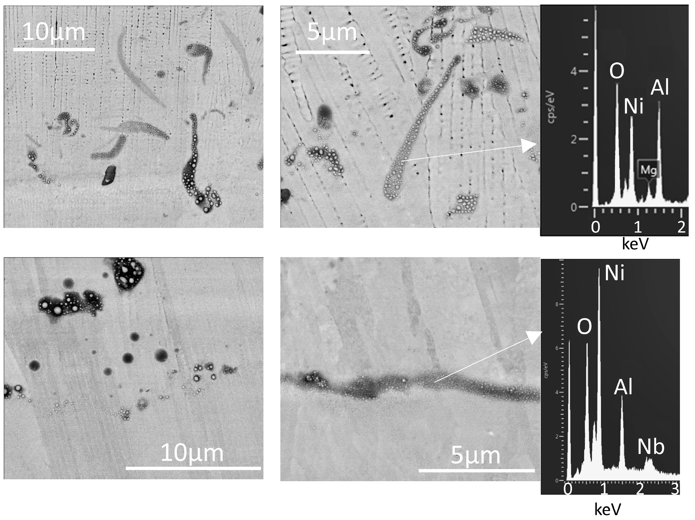
Figure 4.
Secondary electron micrographs of inclusions in deep-etched IN718 LPBF sample, with EDX spectra showing prominent Al and O peaks.
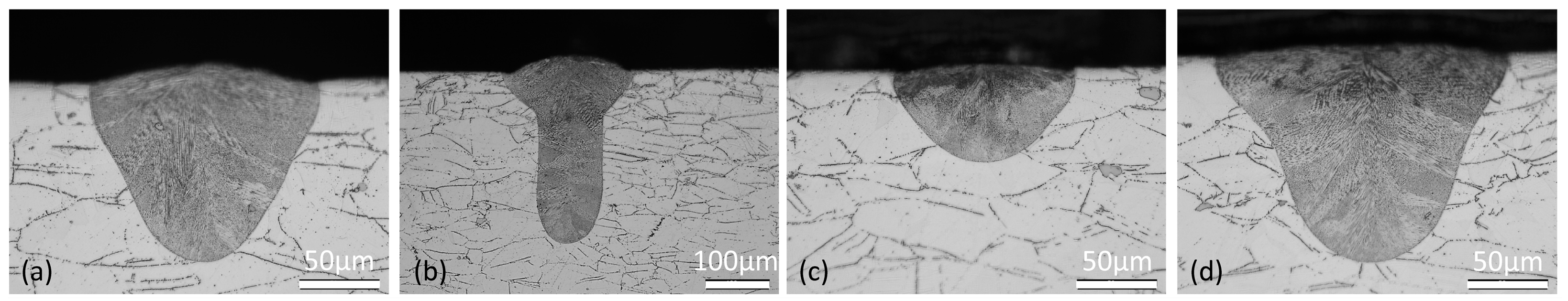
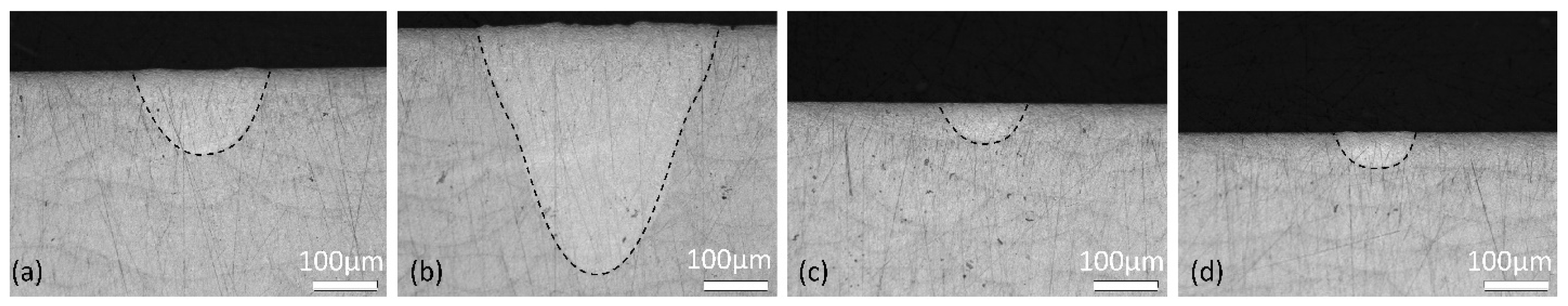
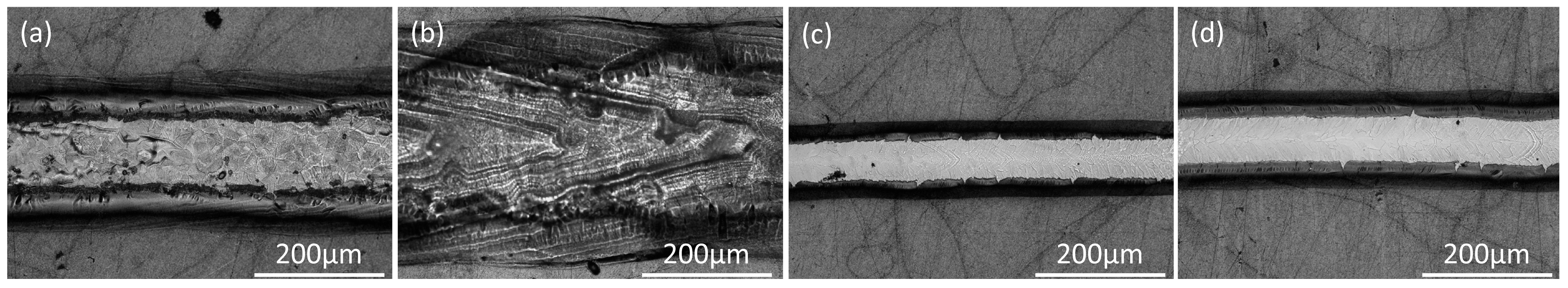
Figure 5.
Cross-sections of IN718 single beads. Melting conditions: (a) STD, (b) Key, (c) Low P, and (d) Low P–low V.
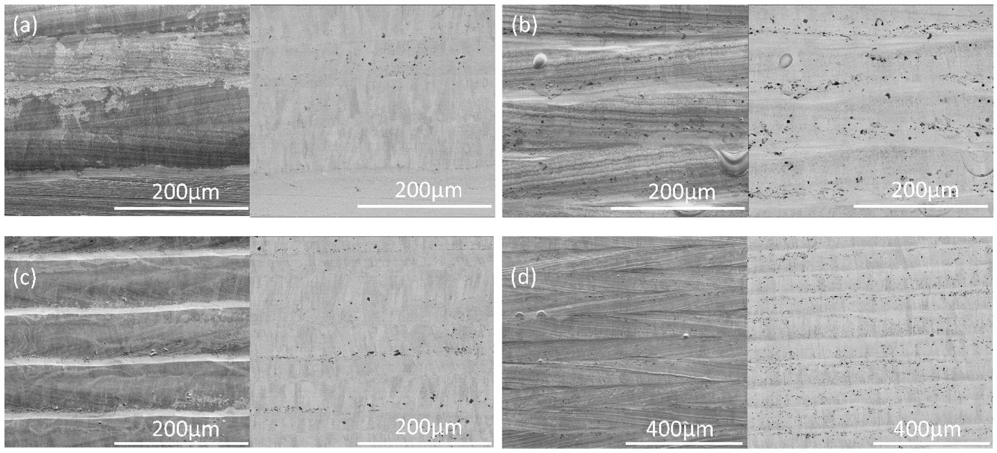
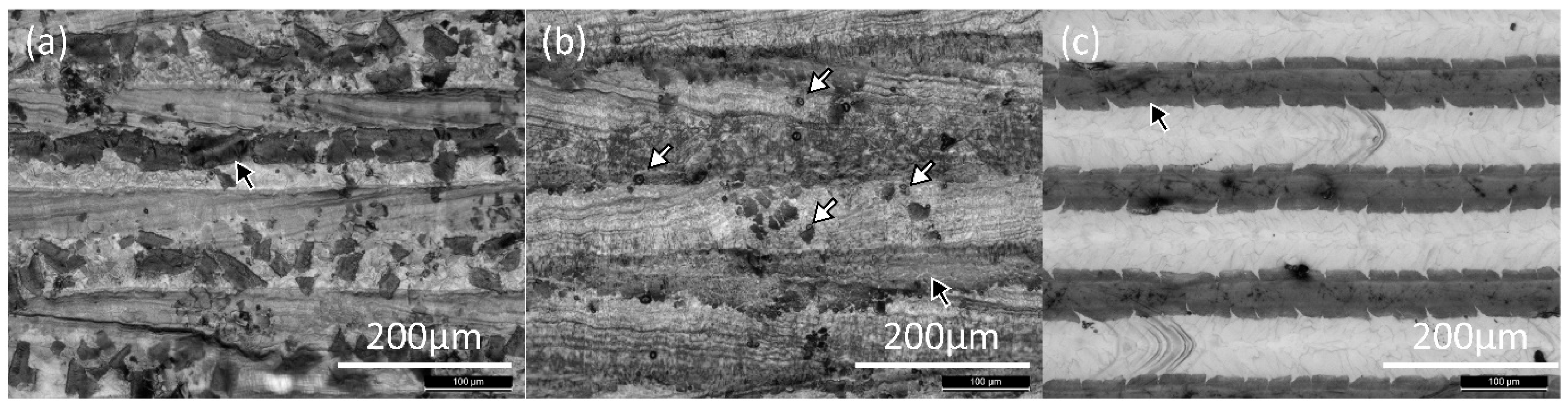
Figure 6.
Optical micrographs of the surface of overlapping laser scans on an IN718 plate, for different melting conditions: (a) STD, (b) Key, (c) Low P, and (d) Low P–low V. The black arrows indicate continuous streaks and the white arrows indicate spherical particles.
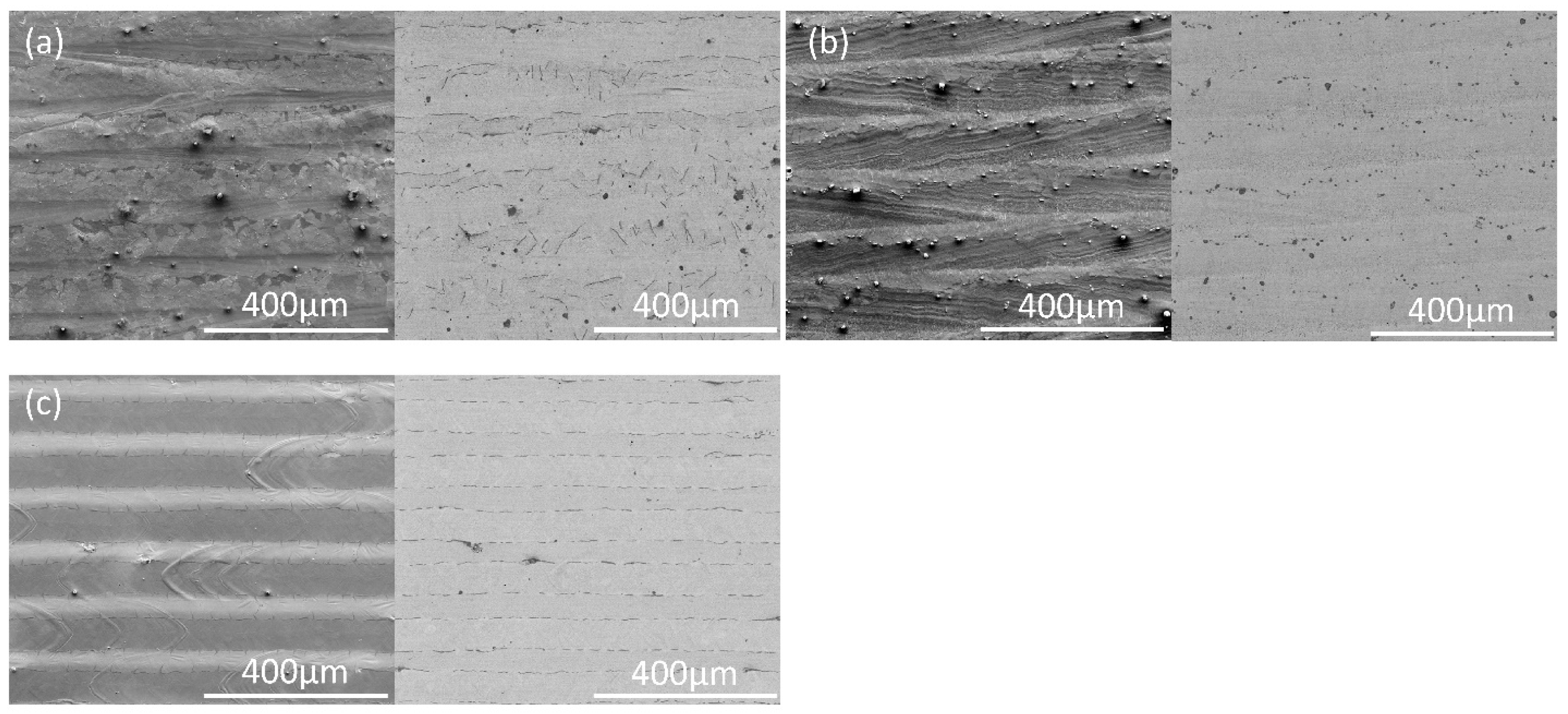
Figure 7.
Scanning electron micrographs of the IN718 plate surfaces melted with different laser conditions: (a) STD, (b) Key, (c) Low P, and (d) Low P–low V. In each pair, a secondary electron image is given on the left and a backscattered electron image on the right.
Figure 8.
Backscattered electron micrographs showing dark areas on laser-remelted IN718 at higher magnification, with EDX spectra of these areas.
Figure 9.
Particle sizes and numbers on laser-remelted IN718 specimens. (a) Oxide particle numbers per unit area. (b) Average particle sizes. (c) Area fraction of oxide particles. (d) Number-based size distribution. Error bars indicate one standard deviation.
Figure 10.
Cross-sections of AlSi10Mg single beads. Process conditions: (a) Std, (b) Key, (c) Low P, and (d) Low P–low V. Broken lines indicate melt pool boundaries.
Figure 11.
Optical micrographs of the surface of the AlSi10Mg samples remelted with different laser conditions: (a) STD, (b) Key, and (c) Low P–low V. The black arrows indicate oxide streaks and the white arrows indicate spherical particles.
Figure 12.
Optical micrographs of the surfaces of the single-scan bead surface of the AlSi10Mg samples remelted under different conditions: (a) STD, (b) Key, (c) Low P, and (d) Low P–low V.
Figure 13.
Scanning electron micrographs of the surfaces of AlSi10Mg parts remelted with different overlapping laser scans. (a) STD, (b) Key, and (c) Low P–low V. In each pair, a secondary electron image is given on the left and a backscattered electron image on the right.
Figure 14.
Higher-magnification scanning electron micrographs of oxides on single bead surfaces for the AlSi10Mg samples, melted under standard conditions (upper pair) and keyholing conditions (lower pair). In each pair, a secondary electron image is given on the left and a backscattered electron image on the right.
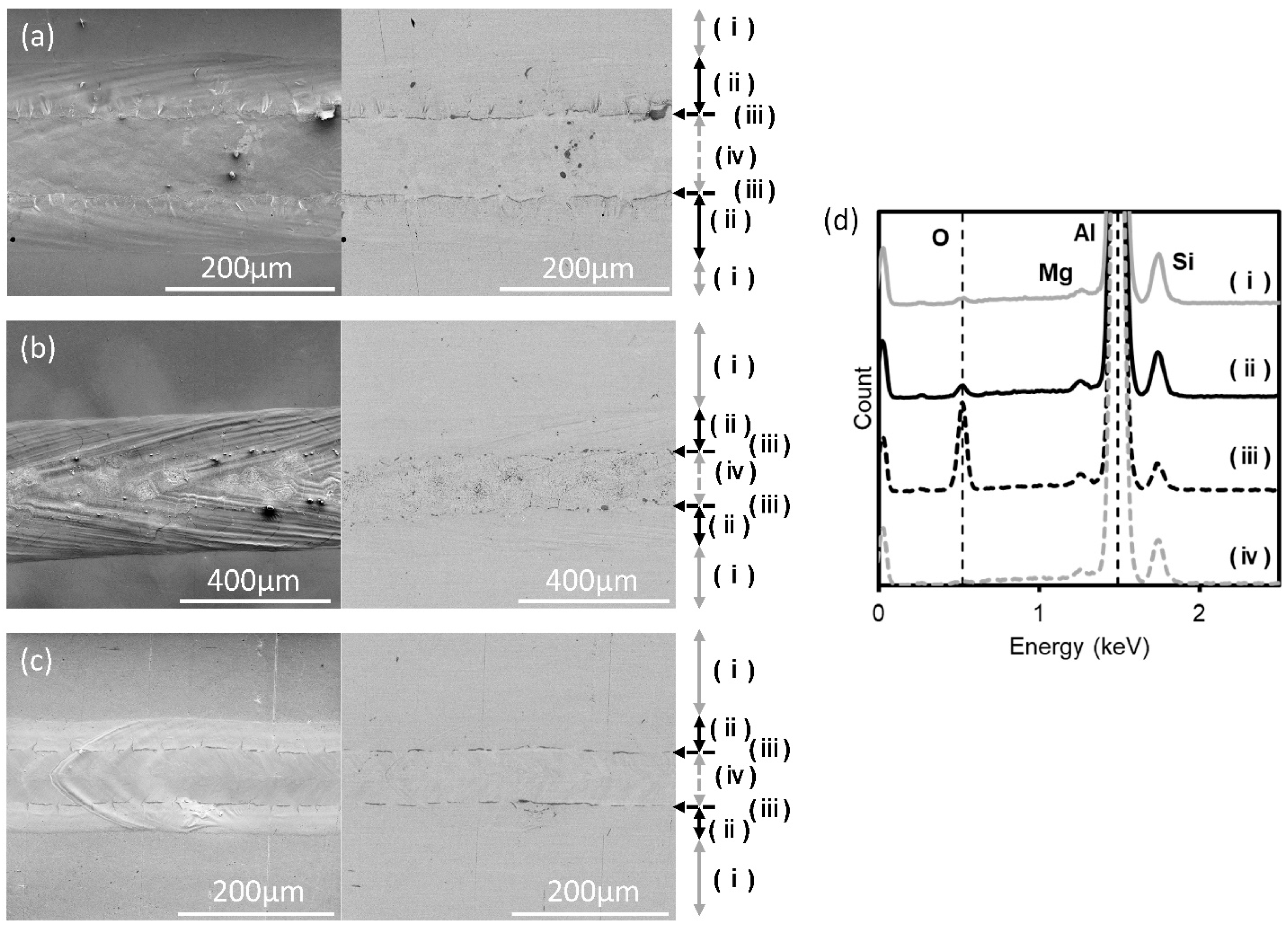
Figure 15.
Scanning micrographs of single beads on AlSi10Mg surfaces (secondary electron images on the left and backscattered electron micrographs on the right), for different melting conditions: (a) STD, (b) keyholing, and (c) Low P–low V conditions. The arrows on the right of the images indicate different regions: (i) unmelted, (ii) oxide band at melt pool edge, (iii) thicker oxides at the edge of the oxide band, and (iv) metal exposed along the center of the melt pool. (d) Representative EDX spectra of the four regions (15 kV acceleration voltage).
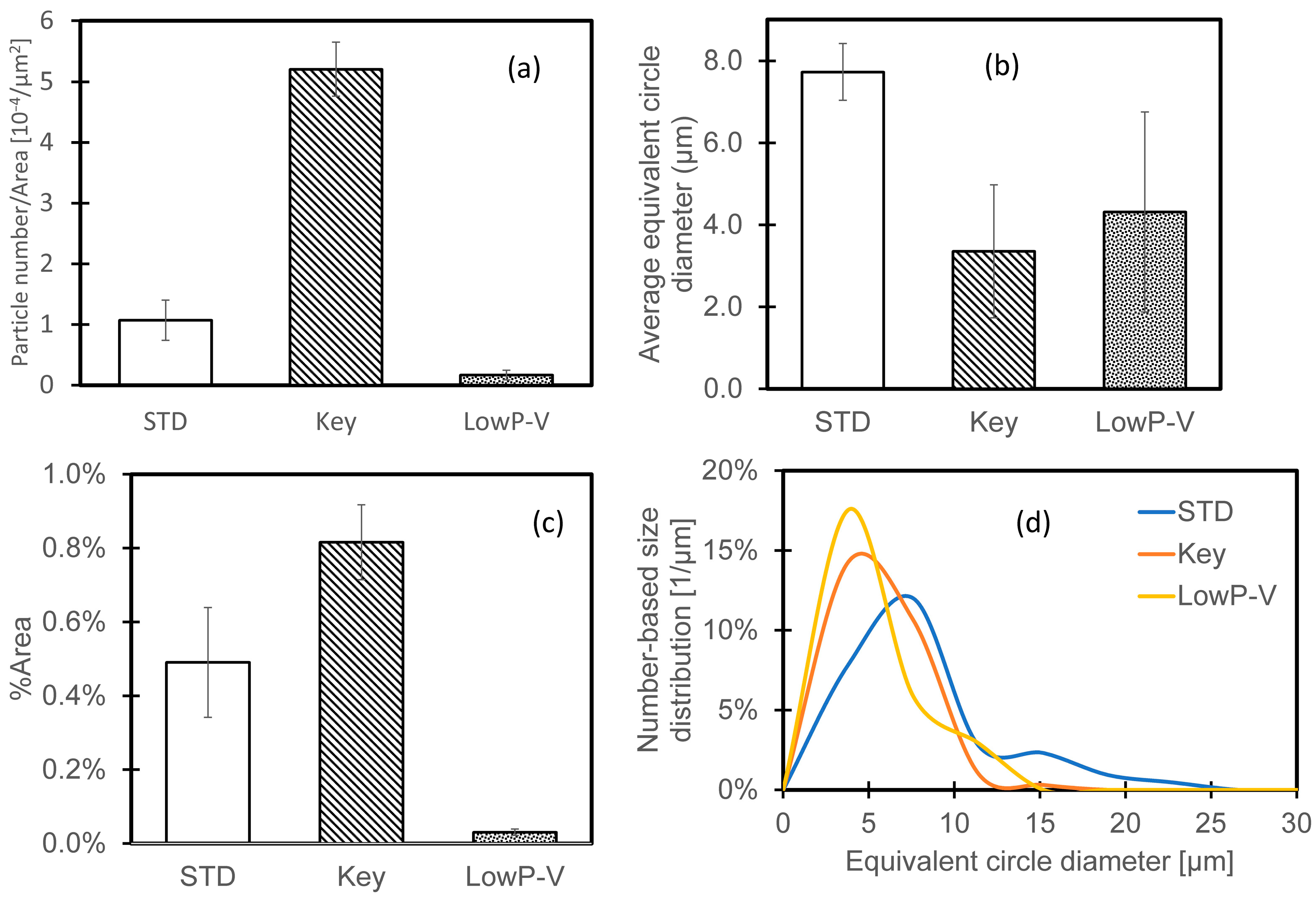
Figure 16.
Oxide particle size analysis results on the surface of laser-remelted AlSi10Mg samples: (a) particle number; (b) average particle; (c) area fraction; (d) number-based particle size distribution. Error bars indicate one standard deviation.
Figure 17.
Optical micrographs of single beads on AlSi10Mg samples that were anodized before laser melting under different conditions: (a) STD, (b) Key, (c) Low P, and (d) Low P–low V.
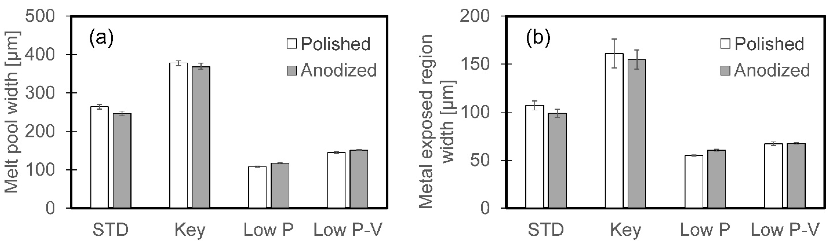
Figure 18.
The widths of (a) the melt pool and (b) metal exposed at the center of the melt pool, for single beads on polished and anodized AlSi10Mg. The error bars indicate one standard deviation.
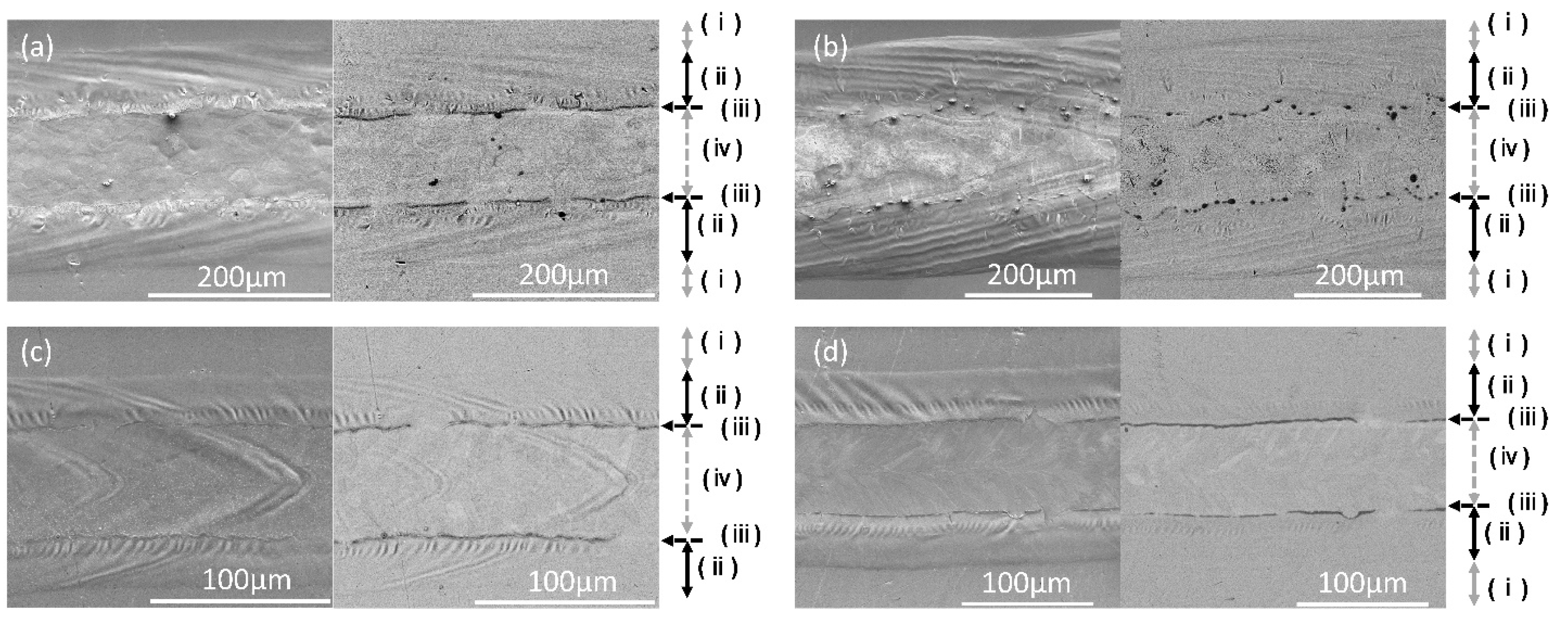
Figure 19.
Scanning electron micrograph images of single beads on the anodized AlSi10Mg samples (secondary electron images on the left and backscattered electron micrographs on the right), for different melting conditions: (a) STD, (b) Key, (c) Low P, and (d) Low P–low V. Arrows to the right of the images indicate the extent of different regions: (i) unmelted region, (ii) oxide band at melt pool edge, (iii) thicker oxides at the edge of the oxide band, and (iv) metal exposed along the center of the melt pool.
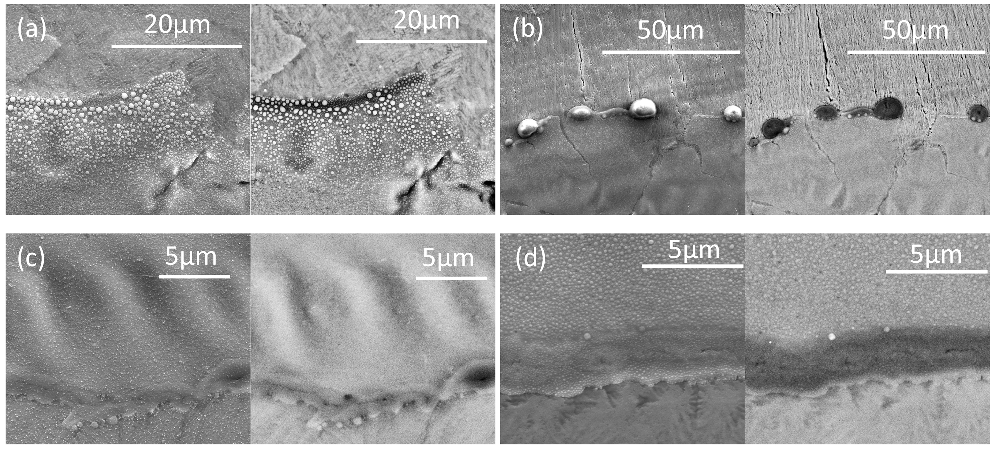
Figure 20.
Higher-magnification scanning micrographs in the thick-oxide regions of single beads on the anodized AlSi10Mg samples, for different melting conditions: (a) STD, (b) Key, (c) Low P, and (d) Low P–low V. In each pair, a secondary electron image is given on the left and a backscattered electron image on the right.
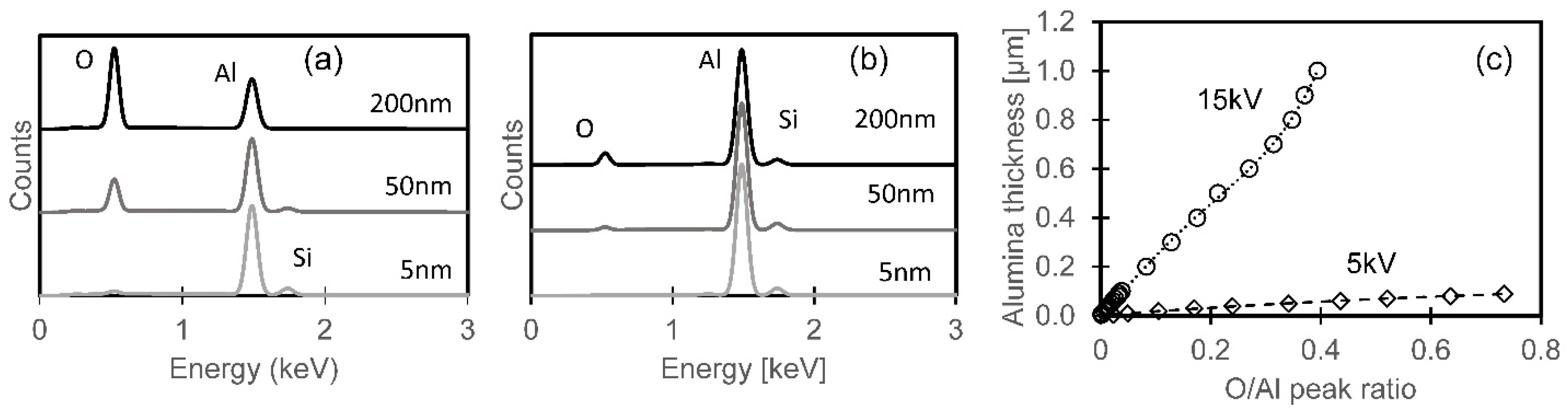
Figure 21.
Simulated EDX spectra for different alumina film thicknesses on bulk AlSi10Mg, at acceleration voltages of (a) 5 kV and (b) 15kV. (c) Relationship between film thickness and simulated O/Al peak count ratio.
Figure 22.
Estimated oxide thickness for each region and melting condition, for polished and anodized AlSi10Mg. Error bars indicate one standard deviation.
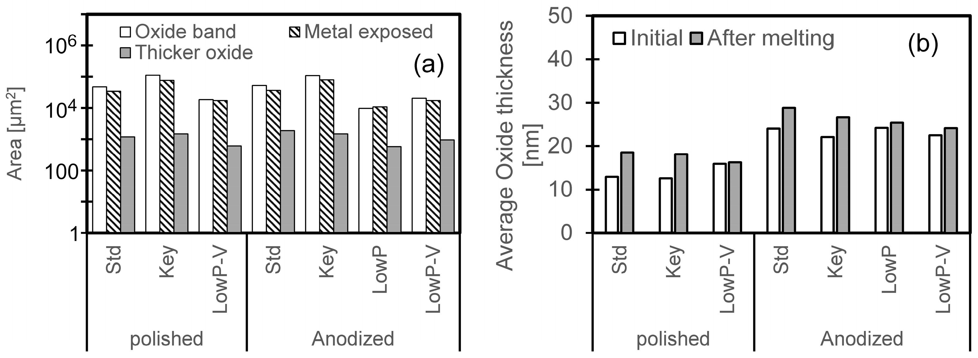
Figure 23.
Oxide areas and thicknesses on polished and anodized AlSi10Mg specimens. (a) Calculated areas of each region. (b) Oxide amount on melted region, expressed as an average thickness for unit area.
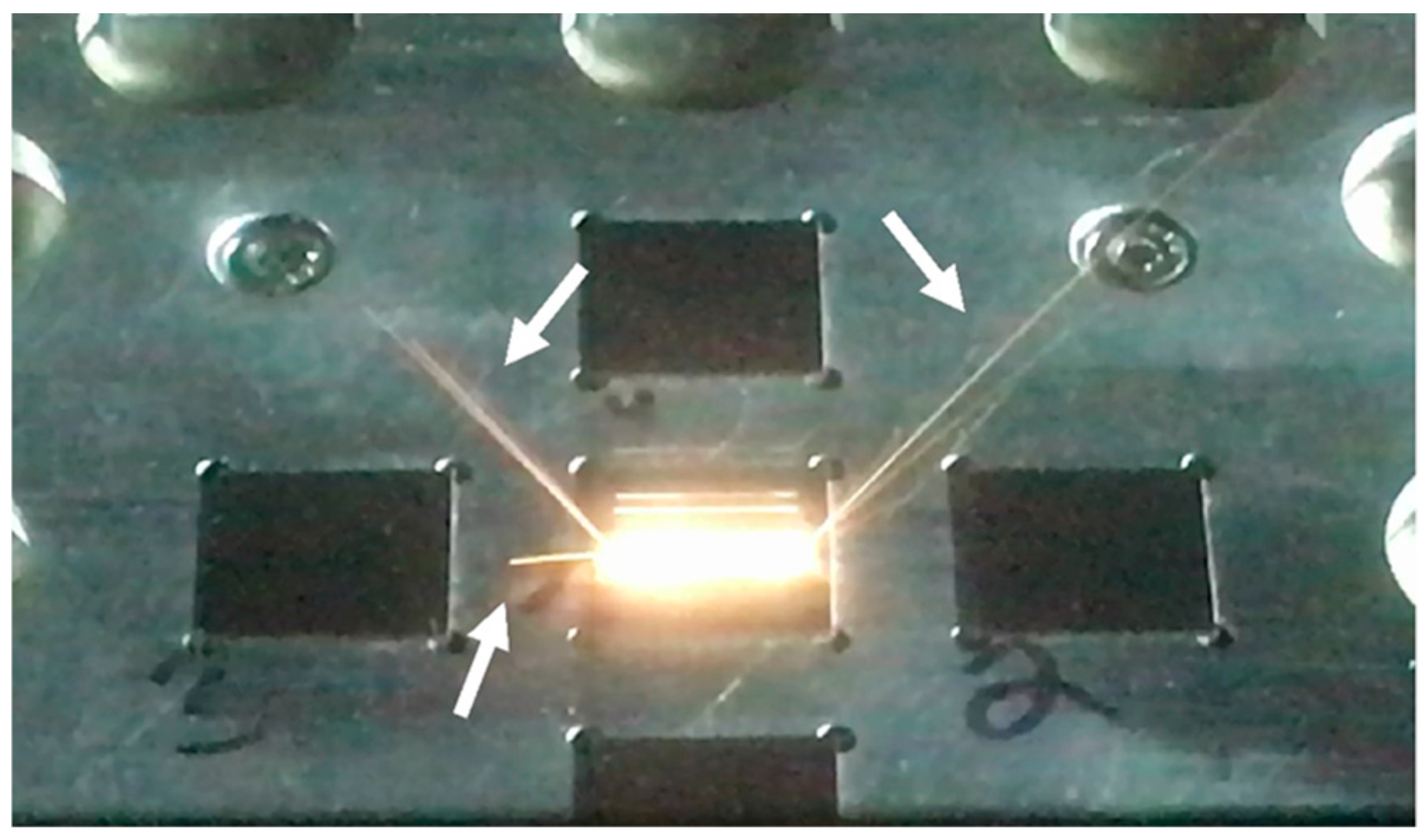
Figure 24.
Image of beam scan of bulk IN718 specimen (standard condition). Arrows indicate spatter ejected from melt pool. Square regions are samples with 20 mm side lengths.
Table 1.
IN718 plate composition.
| Element | Ni | Fe | Cr | Al | Nb | Mo | Ti | Cu | Co |
|---|
| Concentration (wt%) | 53.55 | 17.96 | 18.19 | 0.42 | 5.12 | 2.99 | 1.04 | 0.16 | 0.12 |
Table 2.
Basic parameters of SLM process used in this work.
| Material | Base Temperature | Oxygen Content | Differential Pressure | Hatch Spacing |
|---|
| IN718 | 80 °C | <0.1% | 0.79 mbar | 0.08 mm |
| AlSi10Mg | 200 °C | <0.1% | 0.38 mbar | 0.12 mm |
Table 3.
Beam power, beam speed, and scan times for each condition.
| Material | Melting Condition | Beam Power | Beam Speed | Number of Passes for Multiple-Scan Area |
|---|
| IN718 | Standard (STD) | 285 W | 0.96 m/s | 1 |
| Keyholing (Key) | 285 W | 0.5 m/s | 1 |
| Low power (Low P) | 170 W | 0.96 m/s | 2 |
| Low power and low speed (Low P–low V) | 170 W | 0.5 m/s | 1 |
| AlSi10Mg | Standard (STD) | 370 W | 1.3 m/s | 1 |
| Keyholing (Key) | 370 W | 0.65 m/s | 1 |
| Low power (Low P) | 185 W | 1.3 m/s | 1 |
| Low power and low speed (Low P–low V) | 185 W | 0.65 m/s | 1 |
Table 4.
Parameters used for simulation of EDX spectra.
| Parameter | Value(s) |
|---|
| Beam energy | 5.0 and 15.0 keV |
| Probe dose | 200.0 nA·s |
| Detector | Silicon drift detector |
| Calibration | FWHM[Mn Kα] = 137.0 eV |
| Vacuum conditions | High vacuum |
Table 5.
IN718 single beads: melt-pool dimensions and ratio of melt pool depth to width.
| Condition | Width (W) | Depth (D) | D/W Ratio |
|---|
| µm | µm |
|---|
| STD | 146 | 111 | 0.76 |
| Key | 209 | 268 | 1.28 |
| Low P | 115 | 57 | 0.50 |
| Low P–low V | 185 | 129 | 0.70 |
Table 6.
AlSi10Mg single beads: melt-pool dimensions and ratio of melt pool depth to width.
| Condition | Width (W) | Depth (D) | D/W Ratio |
|---|
| µm | µm |
|---|
| STD | 217 | 132 | 0.61 |
| Key | 371 | 390 | 1.05 |
| Low P | 120 | 53 | 0.44 |
| Low P–low V | 136 | 58 | 0.42 |
Table 7.
Input parameters used for estimation of oxide thickness.
| Material | PO2 | MAl2O3 | ρAl2O3 | T∞ | Tliq | Dgas | vgas |
|---|
| (Pa) | (kg/mol) | (kg/m3) | (K) | (K) | (m2/s) | (m/s) |
|---|
| IN718 | 101.3 | 0.102 | 3990 | 298 | 1598 | 0.00014 | 10 |
| AlSi10Mg | 867 |
Table 8.
Beam conditions and estimated melt pool size and oxide thickness.
| Material | Condition | Vbeam | W | L | LAl2O3 |
|---|
| (m/s) | (μm) | (μm) | (nm) |
|---|
| IN718 | Std | 0.96 | 145 | 1260 | 1.1 |
| Key | 0.50 | 198 | 1270 | 1.9 |
| Low P | 0.96 | 112 | 756 | 0.8 |
| Low P–low V | 0.50 | 150 | 764 | 1.3 |
| AlSi10Mg | Std | 1.30 | 222 | 314 | 0.2 |
| Key | 0.65 | 282 | 343 | 0.3 |
| Low P | 1.30 | 141 | 172 | 0.1 |
| Low P–low V | 0.65 | 171 | 189 | 0.2 |


