Abstract
This study proposes a Sn58Bi/SAC305 layered composite solder designed for low-temperature applications. By alternating high-melting SAC305 and low-melting Sn58Bi layers, the composite achieves a liquidus temperature of ~180 °C, comparable to traditional Sn-Pb solder. Synchrotron X-ray imaging reveals dynamic interfacial interactions, including partial dissolution of SAC305 into molten Sn58Bi and Bi diffusion, mitigating segregation and forming defect-free interfaces with cellular structures. The 7-layer composite exhibits a peak shear strength of 44.3 ± 0.8 MPa at 200 °C, surpassing single Sn58Bi (41.8 ± 1.1 MPa) and SAC305 (31.6 ± 1.4 MPa), attributed to the refined microstructure and uniform dispersion of Ag3Sn phases. Fracture analysis indicates mixed ductile–brittle failure modes influenced by intermetallic compounds (IMCs). This work provides insights into the role of layered structures in controlling element diffusion and interfacial reactions, advancing the design of low-temperature lead-free solders.
1. Introduction
Traditional Sn-Pb solders have been commonly used in electronic packaging for their superior electronic connectivity and mechanical support properties [1,2]. However, the electronics industry has been actively seeking environmentally friendly, lead-free alternatives due to lead toxicity. Sn-rich solders are promising candidates due to their high strength, excellent thermal fatigue resistance, and anti-creep characteristics [3,4]. Among these, the Sn-9Zn lead-free solder alloy, with a melting temperature of 198 °C, which is close to that of Sn-37Pb (183 °C), is considered one of the most viable replacements for eutectic Sn-Pb solder [5]. However, Sn-Zn alloys face significant challenges, primarily due to the high oxidation tendency of Zn, which negatively impacts the solder’s oxidation resistance, wettability, and corrosion resistance [6,7]. In contrast, Sn-Ag-Cu alloy solders demonstrate outstanding solderability, remarkable creep resistance, and high-level thermal fatigue reliability [8,9]. They are the most widely used lead-free solders and are regarded as strong alternatives to Sn-Pb solders [10]. Nevertheless, Sn-Ag-Cu alloys have higher melting points, particularly the eutectic Sn-Ag-Cu, which melts at 217 °C, 34 °C higher than Sn-37Pb. This elevated reflow temperature can cause substrate warping and excessive growth of brittle intermetallic compounds (IMCs), undermining the reliability of solder joints [11]. Reducing the reflow temperature can effectively address this issue. The SnBi eutectic solder, a commonly employed low-temperature solder, has a melting point of merely 139 °C [12,13,14,15]. Despite its low cost, the brittleness of Bi in the SnBi eutectic solder gives rise to problems such as poor solder joint ductility, restricting its widespread application [16,17,18]. Some researchers have endeavored to acquire composite solders with enhanced performance by blending these two types of solders [19]. However, the maximum Bi content in these composites is merely 3.0%, resulting in an insignificant reduction in the melting point. Others have implemented a step-by-step assembly of SAC and SnBi to fabricate mixed-assembly solder joints with varying degrees of fusion, aiming to lower the connection temperature [20]. Nevertheless, the soldering process on the SAC side still necessitates a relatively high-temperature environment. Therefore, there is an urgent need to develop lead-free solders with a soldering temperature similar to that of Sn-Pb to meet the requirements of existing circuit boards, components, and production lines.
In this study, SAC305 and Sn58Bi were used to prepare a layered composite solder, endowing it with low-temperature soldering characteristics and high strength. Synchrotron radiation technology was employed to observe the dynamic melting process of the layered composite solder, and the mechanism of solid–liquid interface formation leading to the cellular structure was explored. Additionally, the effects of soldering temperature on the microstructure and shear properties of the joints were investigated, and the results were compared with those of joints made using single solder, Sn58Bi and SAC305. This research provides a viable solution for developing low- and medium-temperature solder.
2. Materials and Methods
2.1. Design Principles and Fabrication of Sn58Bi/SAC305 Layered Composite Solder
The layered composite solder was designed with a fusion temperature close to the melting point of Sn37Pb solder, corresponding to a liquid-phase line temperature of approximately 180 °C. Based on the mass conservation of Bi and Sn before and after soldering, and using the SnBi phase diagram, the volume ratio of the two solders before reflow was approximated as follows:
The outermost layer was designed with SnBi to reduce the soldering temperature. The final design incorporated 3, 5, 7, and 9 layers, with Sn58Bi and SAC305 layer thicknesses set to 50 μm and 75 μm, respectively, according to the volume ratio.
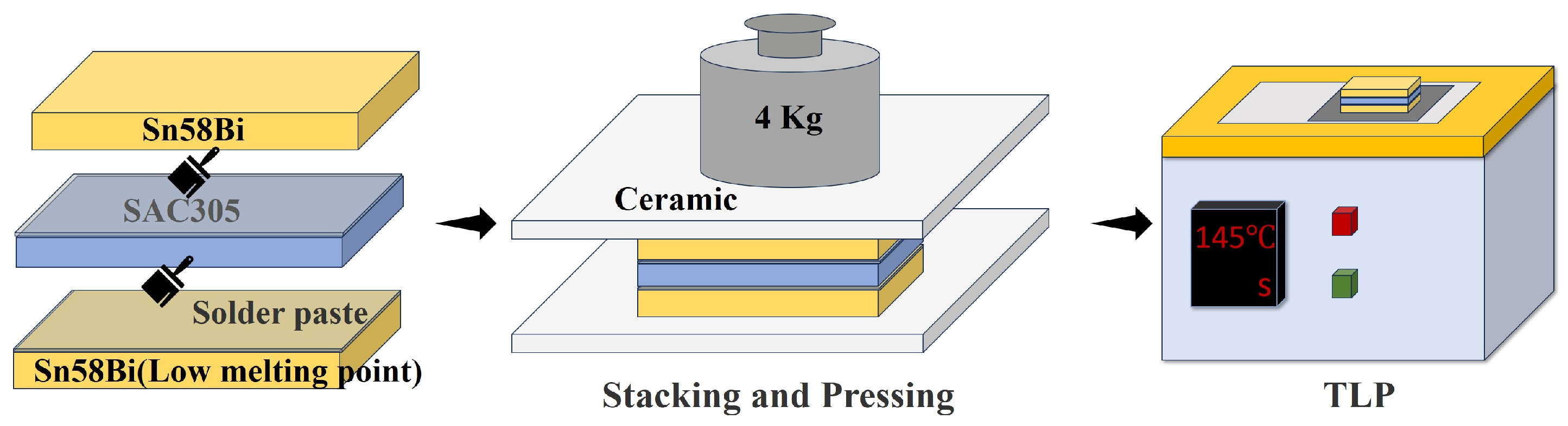
The preparation process is outlined in Figure 1. First, Sn58Bi and SAC305 solder were rolled into 50 ± 2 μm and 75 ± 2 μm thick sheets. These sheets were then cut into (10 ± 0.1) × (5 ± 0.1) mm pieces, cleaned with anhydrous ethanol and deionized water to remove contaminants, and coated with a thin, uniform layer of Rosin-based flux on the contact surfaces. The sheets were stacked and placed between two ceramic sheets. Then, at room temperature, they were pressurized with 4 kg weights for 1 h to ensure tight bonding and remove excess flux. A titanium sheet was used as the substrate to prevent the loss of Sn58Bi during melting. The solder was then heated on a hotplate at 145 °C for a specified period to establish a metallurgical bond between Sn58Bi and SAC305. To minimize the influence of layer thickness on heat transfer, the heating time was set to 20 s for 3 layers, 25 s for 5 layers, 30 s for 7 layers, and 35 s for 9 layers, ultimately forming a composite solder with a layered structure.
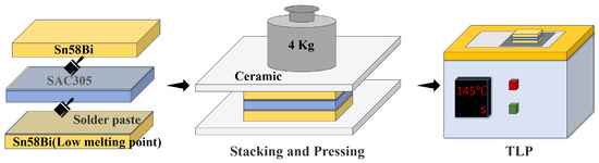
Figure 1.
Schematic diagram of the preparation method of layered composite solder.
For comparison, a melt-cast solder with the same composition as the 7-layer layered composite solder was also prepared. Sn58Bi and SAC305 were mixed in a 13/12 mass ratio, melted at 250 °C for 10 min, and cooled to obtain the uniform melt-cast solder.
2.2. Microstructural and Elemental Distribution Characterization
The prepared layered composite solder sheets were cut into small pieces measuring (5 ± 0.1) × (2 ± 0.1) mm and inlaid with epoxy conductive adhesive onto a conductive metal block. After grinding and polishing, the microstructure of the solder was observed using an electron probe microanalyzer (JXA-8530, JEOL, Tokyo, Japan). The interlayer bonding and elemental distribution of the solder with different numbers of layers were investigated using backscattered electron imaging (BSE) and line scan analysis.
2.3. Soldering Process and Joint Performance Evaluation
Copper substrates sized (10 ± 0.3) × (5 ± 0.3) mm were used for soldering experiments. These substrates were polished progressively with 1000 to 2000 mesh sandpaper and further polished using 1.5 μm diamond paste until they were scratch-free and bright. The substrates were ultrasonically cleaned with a 5-vol% HCl solution for 30 s to remove oxide layers, followed by cleaning with deionized water and drying.
The prepared layered composite solder and melt-cast solder sheets were cut into small pieces of (5 ± 0.1) × (2 ± 0.1) mm, placed on Cu substrates, and reflowed at 160 °C, 180 °C, and 200 °C for 40 s each. After reflow, the cross-sections of the solder joints were polished and observed using the EPMA-1600 to analyze the microstructure.
2.4. Synchrotron X-Ray Real-Time Imaging Experiment
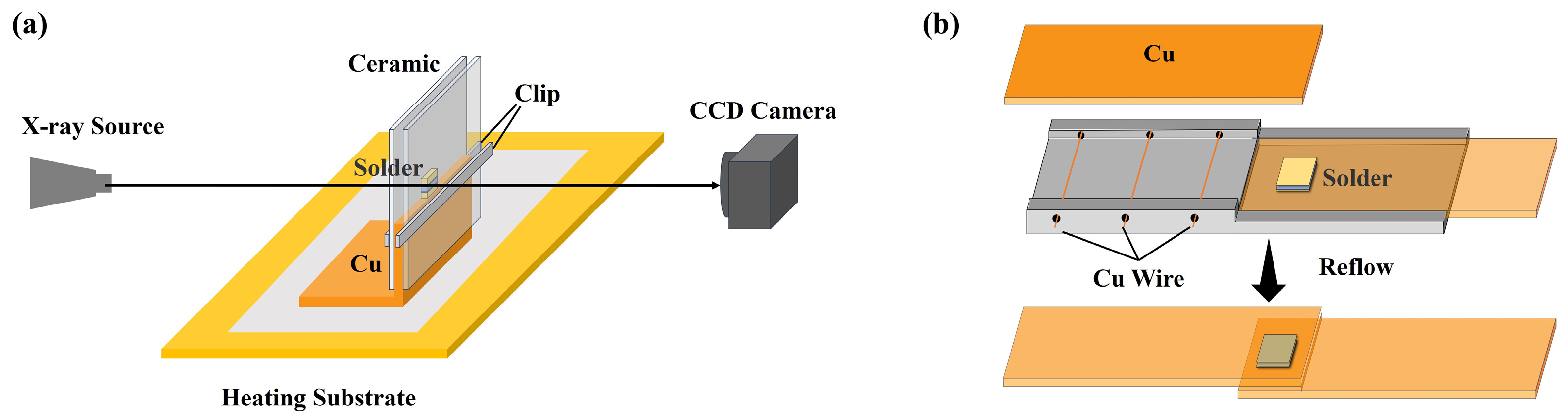
The Shanghai Synchrotron Radiation Facility (SSRF, Shanghai, China), with the specific use of the BL13W1 beamline, was used to observe the interaction between the two solders during the heating and holding process of the layered composite solder. These data were combined with electron backscattering images to explain the evolution mechanism of the microstructure. The synchrotron radiation samples were prepared, as shown in Figure 2a. Before soldering, the copper foil cross-sections were polished to remove scratches, and the copper foil was bent to support the samples and enhance thermal conductivity. The clamping edges of the fixture were tightly attached to the contact edges of the solder sheet and copper foil to prevent the flow of liquid solder into the gap during soldering. The test beam energy was set to 25 keV, and the imaging resolution was 0.37 μm/pix.

Figure 2.
Schematic diagram of test sample preparation: (a) synchrotron radiation sample, (b) shear experiment lap joints.
2.5. Evaluation of Shear Properties of Solder Joints
Lap joints were prepared to evaluate the shear properties of solder joints. As shown in Figure 2b, Cu wires with the same diameter as the thickness of solder pieces were used to control the spacing of the substrates. The copper substrates were coated with flux and placed on a hotplate for reflow at 160 °C, 180 °C, 200 °C, and 220 °C for 40 s.
Shear experiments were performed using an Instron 5982 tester (Instron, Norwood, MA, USA), and shear strength was determined by the ratio of shear load to fracture area. Fracture morphology was analyzed using scanning electron microscopy (SEM), and elemental composition was assessed using energy dispersive spectroscopy (EDS). For this study, a tensile rate of 0.3 mm/min was selected for the experiments.
3. Results and Discussion
3.1. Microstructure of Layered Composite Solder
Layered composite solder sheets with 3-, 5-, 7- and 9-layer structures were prepared through a layered stacking and controlled diffusion process. The microstructures and compositions of these materials were analyzed to assess their quality.
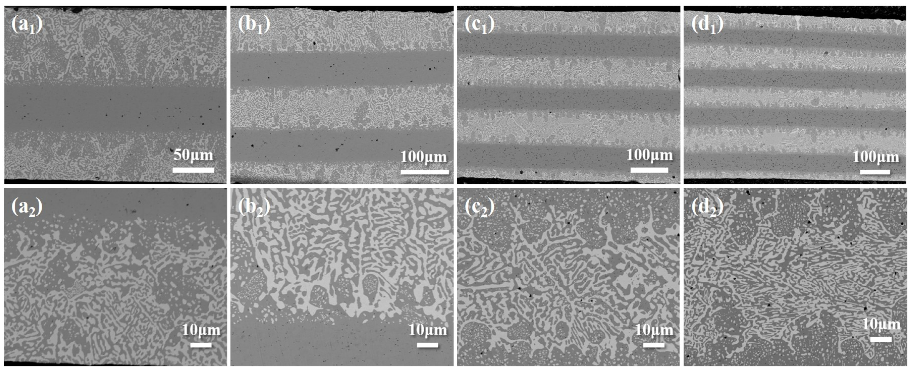
The backscattered image of the cross-section of the prepared layered composite solder sheets is shown in Figure 3. As per the design, the outermost layers consist of Sn58Bi with a reticulated eutectic structure. In Figure 3(a1), the three-layer solder is composed of a sandwich structure of Sn58Bi/SAC305/Sn58Bi, where the white region in the Sn58Bi layer represents the Bi-rich phase, the gray region is β-Sn, and the SAC305 layer appears as a uniform gray. The structures of the other layers are similar. Figure 3(a1–d1) show that the 3-layer, 5-layer, 7-layer, and 9-layer solders maintain a well-defined layered structure with no visible pores or residual flux at the interfaces, indicating strong interlayer bonding. Higher-magnification images (Figure 3(a2–d2)) reveal that elemental diffusion has occurred at the interface, forming a sub-eutectic structure, while the SnBi layer, far from the SAC305 layer, retains its original reticulated eutectic structure.

Figure 3.
Backscattered images of the cross-section of layered composite solder sheets: (a1,a2) 3-layer, (b1,b2) 5-layer, (c1,c2) 7-layer, (d1,d2) 9-layer.
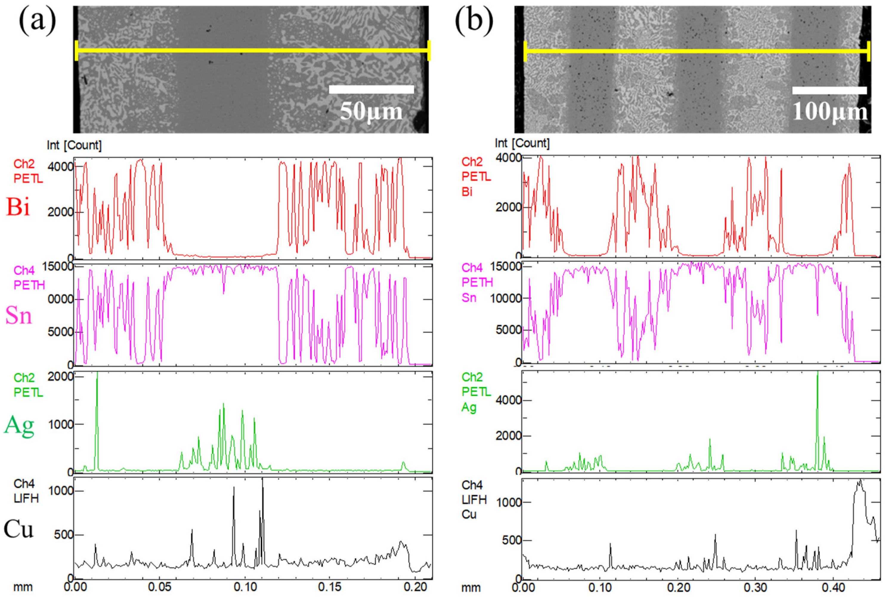
Line scan analyses were conducted along the vertical interface direction on the cross-sections of the 3-layer and 7-layer solders, as shown in Figure 4. The elemental distribution aligns with the observed microstructure. Due to the low heating temperature and short duration, metallurgical bonding between the SnBi and SAC305 layers occurs primarily at the interface, with insufficient diffusion of the elements. Bi predominantly resides in the SnBi layer, while Ag and Cu are primarily located in the SAC305 layer. A notable concentration gradient exists between the Sn58Bi and SAC305 solders, with substantial differences in element distribution.
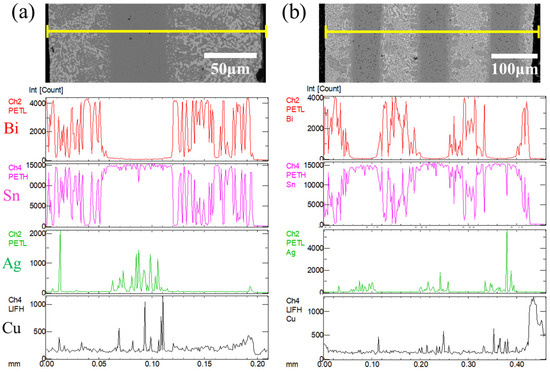
Figure 4.
Line scan results of the cross-section of layered composite solder sheets: (a) 3-layers, (b) 7-layer.
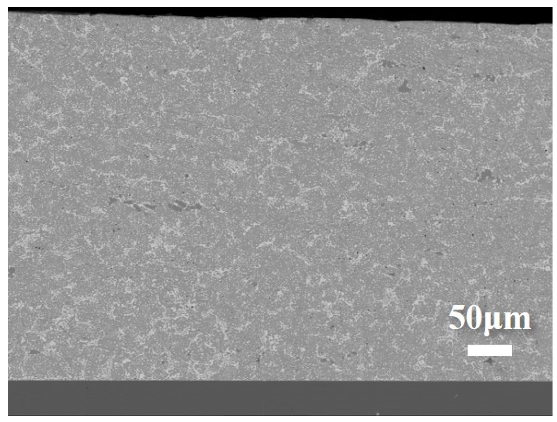
Table 1 shows the composition of the melt-cast solder: Sn-32.2Bi-1.4Ag-0.2Cu. The microstructure, shown in Figure 5, displays a diffusely distributed Bi-rich phase without the characteristic reticular structure. This is because the melt-cast solder is prepared by melting Sn58Bi and SAC305 at 250 °C for 10 min. The high temperature and long melting time allow the components to mix thoroughly. When cooled, the elements solidify from a well-mixed state, leading to a homogeneous microstructure with a diffusely distributed Bi-rich phase.

Table 1.
The composition of the melt-cast solder.
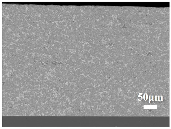
Figure 5.
Microstructure of the melt-cast solder (backscattered image).
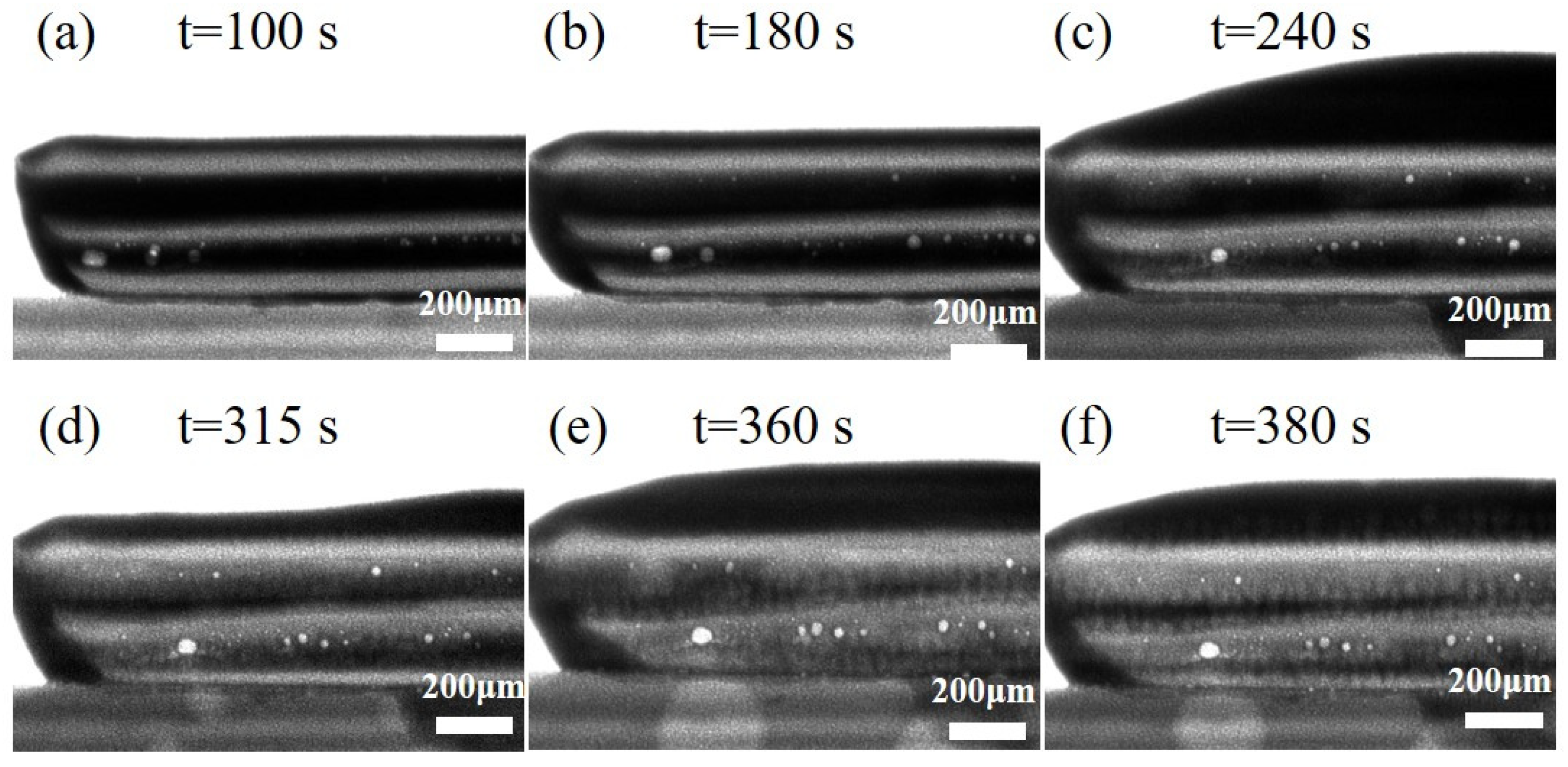
3.2. In Situ Observation of Interfacial Fusion Dynamics During Reflow
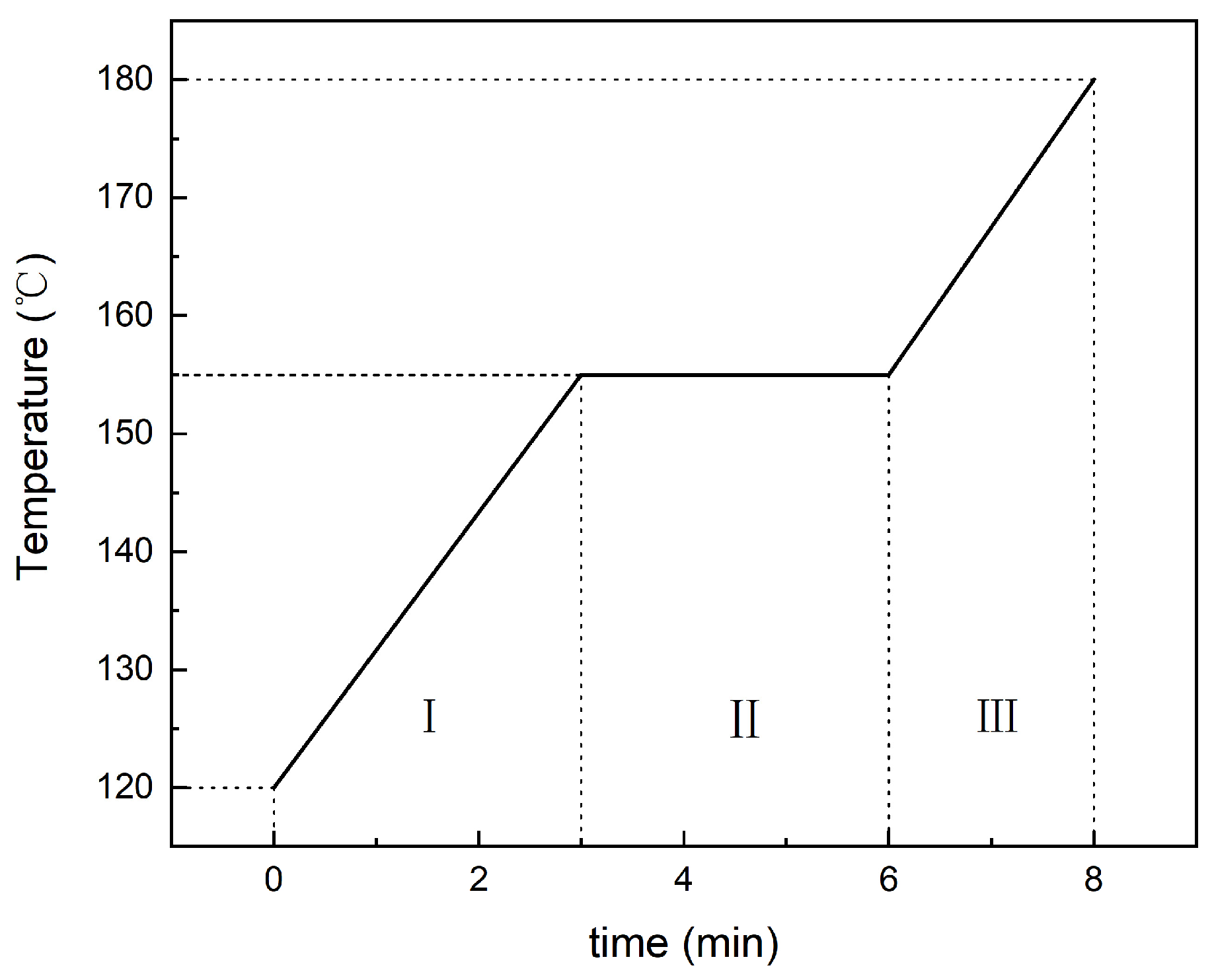
The reflow process of the 7-layer composite solder sheet with Cu substrate was observed in situ using the SSRF. The reflow temperature profile is shown in Figure 6, and synchrotron radiation images at different stages of the reflow process are shown in Figure 7. In these images, the black color represents the Sn58Bi layer, the brighter gray color represents the SAC305 layer, and the lowest layer corresponds to the Cu substrate.
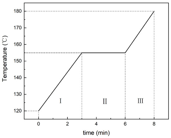
Figure 6.
Reflow temperature profile of layered composite solder joints in synchrotron radiation experiments.
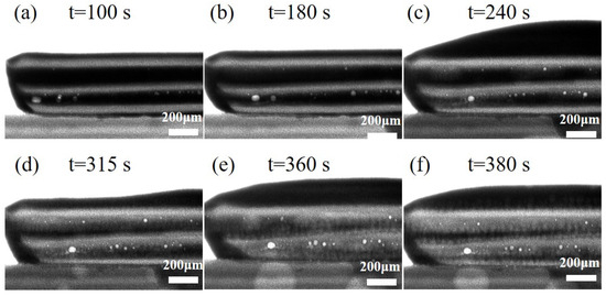
Figure 7.
Time-resolved synchrotron radiation imaging of interfacial fusion in 7-layer solder with Cu substrate: (a) t = 100 s, (b) t = 180 s, (c) t = 240 s, (d) t = 315 s, (e) t = 360 s, (f) t = 380 s.
In Stage I, as the reflow temperature increased, the Sn58Bi solder melted at 140 °C and rapidly transitioned into a liquid state (Figure 7a). SAC305 began to dissolve into the molten Sn58Bi, and with a further temperature increase, the amount of dissolved SAC305 expanded, causing the liquid-phase region to widen (Figure 7b). Stage I concluded when the temperature reached 155 °C.
Stage II involved holding the temperature at 155 °C for 3 min. During this stage, SAC305 continued to dissolve into the molten Sn58Bi, and the liquid-phase region continued to expand. After 60 s, dissolution at the solid–liquid interface ceased, and Sn reached its saturation limit in the liquid phase. At this point, the Bi content in the solid and liquid phases reached the values corresponding to the solid-phase and liquid-phase lines of the SnBi phase diagram at 155 °C, respectively. The liquid-phase region reached its maximum size. Due to surface tension and the wetting effect of the liquid phase on the solid phase, the liquid phase primarily flowed toward the top layer, causing the liquid volume in the top layer to gradually thicken (Figure 7c). As the holding time increased, a cellular solidification structure appeared on the surface of the SAC305 layer (Figure 7d,e). This was attributed to the diffusion of Bi into the SAC305 layer, which reduced the melting point of the SAC305 surface, inducing supercooling at the solid–liquid interface. This created solidification conditions similar to those of pure metals under a negative temperature gradient, leading to localized bulging of the interface. However, due to the narrow subcooling zone, the solidified portion was confined to this zone and failed to grow sufficiently into the liquid phase, eventually forming a cellular structure.
In Stage III, the temperature was increased to 180 °C. At this point, the liquid-phase region continued to expand, and cytosolic interfaces between the layers remained (Figure 7f).
In summary, synchrotron radiation experiments provided dynamic observations of the interfacial fusion of the layered composite solder during reflow. The cellular structure began to form during both the holding and warming stages.
3.3. Soldering Performance of Layered Composite Solder
The composition of intermetallic compounds in the post-soldering microstructure of the layered solder was analyzed, and the corresponding atomic percentages are presented in Table 2. Based on the types and atomic percentages of the elements present, it is inferred that the white-bordered phases “1” and “2” in Figure 8a are Ag3Sn, while the dark gray phases “3” and “4” are Cu6Sn5. The phase distribution in the cross-sectional microstructures of the layered solder joints and the melt-cast solder joints is shown in Figure 8a,b. The gray base corresponds to the Sn-rich phase, while the reticular and granular white phases represent the Bi-rich phase. The gray particles with white boundaries in the matrix are Ag3Sn, and the dark gray particles are Cu6Sn5.
Table 2.
Atomic percentages of intermetallic compounds in the cross-section of layered solder joints (at. %).
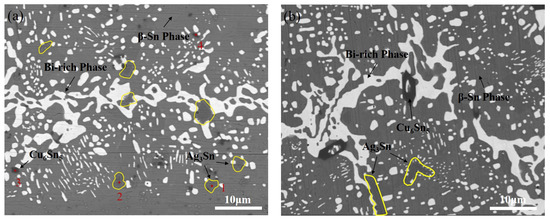
Figure 8.
Phase distribution in (a) 7-layer and (b) melt-cast solder joints after 180 °C reflow. The yellow areas represent Ag3Sn, and the numbers indicate the points corresponding to the composition analysis.
3.3.1. Fusion Behavior of Sn58Bi/SAC305 Layered Solder After Soldering
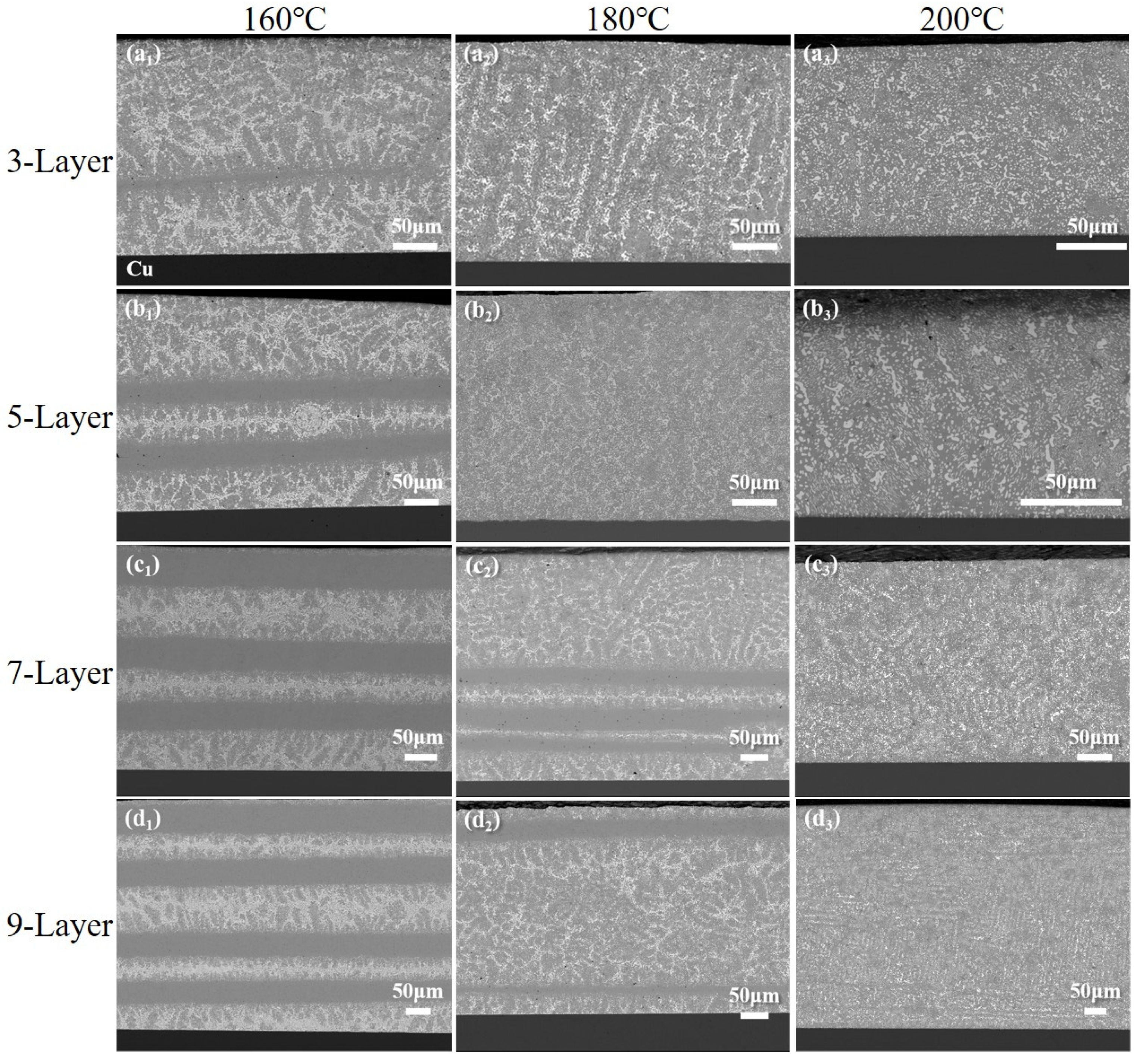
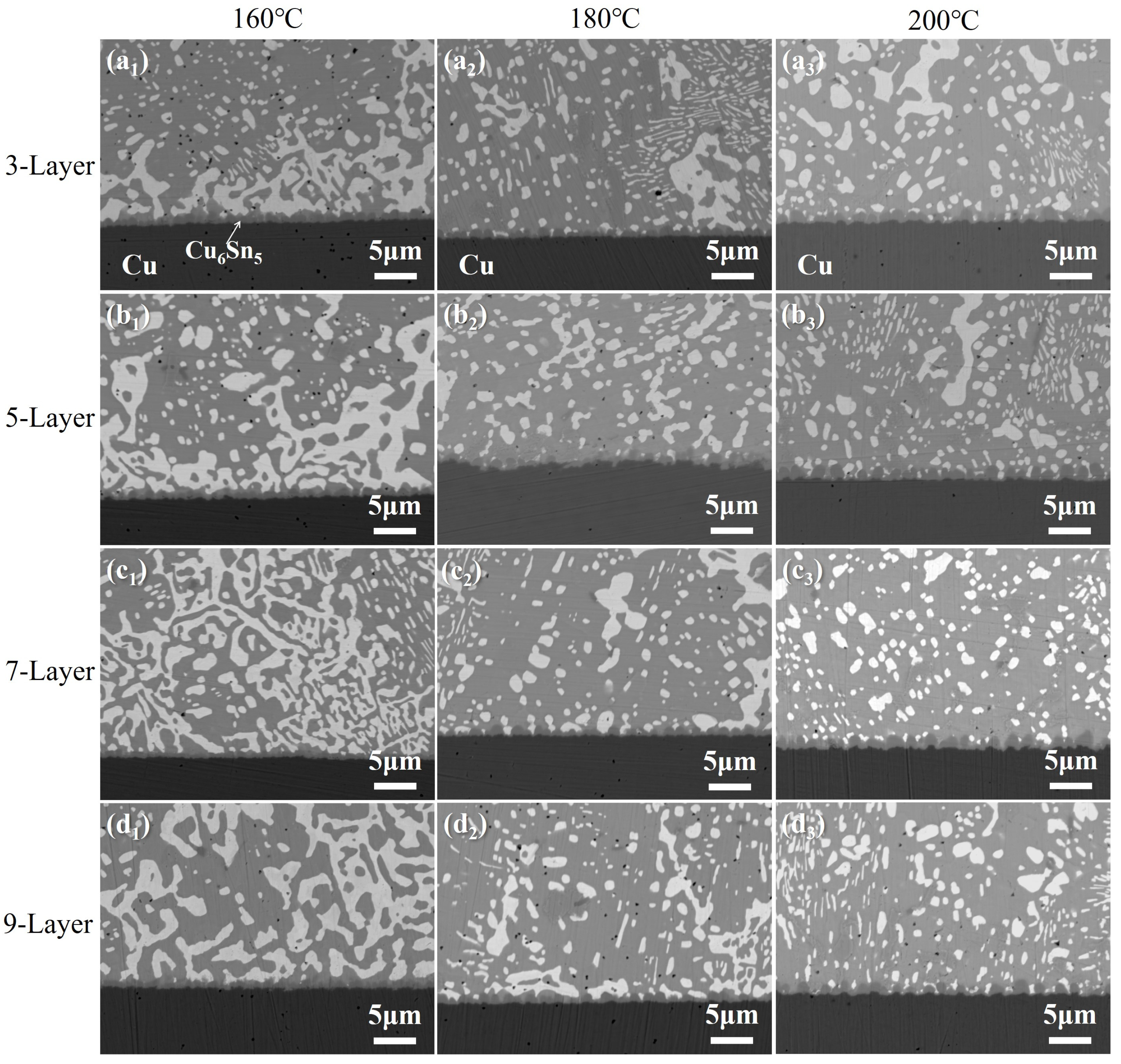
To further investigate the soldering performance of Sn58Bi/SAC305 layered composite solder, Electron Probe Micro-Analyzer (EPMA, JXA-8530, JEOL, Tokyo, Japan) was employed to carefully observe and analyze the cross-sectional microstructure of three-, five-, seven-, and nine-layer composite solders after soldering with Cu substrate at different temperatures. The specific results are presented as follows.
After soldering at 160 °C, the cross-sections of the solder are shown in Figure 9(a1–d1). The 3-, 5-, 7-, and 9-layer solders retained their layered structure, with the SnAgCu layer in the 3- and 5-layer materials being thinner and exhibiting a higher degree of fusion.
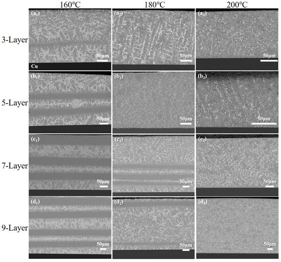
Figure 9.
Comparison of the fusion of layered composite solder/Cu joints with varying layer counts after reflow at 160 °C, 180 °C and 200 °C: (a1,a2,a3) 3-layer, (b1,b2,b3) 5-layer, (c1,c2,c3) 7-layer, (d1,d2,d3) 9-layer.
After soldering at 180 °C, the cross-sections of the solder are shown in Figure 9(a2–d2). Although the melting point of the SnAgCu alloy has not been reached, the layered structure of the 3- and 5-layer solders has completely disappeared, with the SnBi and SnAgCu layers fully fused to form a SnBiAgCu sub-eutectic structure. In contrast, the SnAgCu layer in the 7- and 9-layer materials remains only partially intact, and its position has changed. This change is primarily attributed to the increased temperature, which accelerates the element diffusion rate, allowing more Bi to diffuse into the SnAgCu layer. The diffusion of Bi lowers the melting point of the SnAgCu layer, leading to the generation of a more liquid phase and a reduction in the residual solid phase. The complete mixing temperatures for the 3-, 5-, 7-, and 9-layer solders were found to be 172 °C, 176 °C, 181 °C, and 182 °C, respectively. Therefore, at 180 °C, which is higher than the liquid-phase line temperature of the 3- and 5-layer materials, the SnAgCu layer in these materials is completely dissolved. However, in the 7- and 9-layer materials, the SnAgCu layer is only partially dissolved at 180 °C due to their higher complete mixing temperatures. The position shift in the SnAgCu layer is mainly influenced by the combined effects of liquid-phase wetting, surface tension, and mobility.
After soldering at 200 °C, the cross-sections of the solder are shown in Figure 9(a3–d3). At this temperature, the SnAgCu layers in all solders are completely dissolved, and the solder exhibits a uniform and consistent structure. This indicates that, at 200 °C, the components in the solder are fully mixed, achieving an optimal fusion state, which provides a solid microstructural foundation for the optimization of solder joint performance.
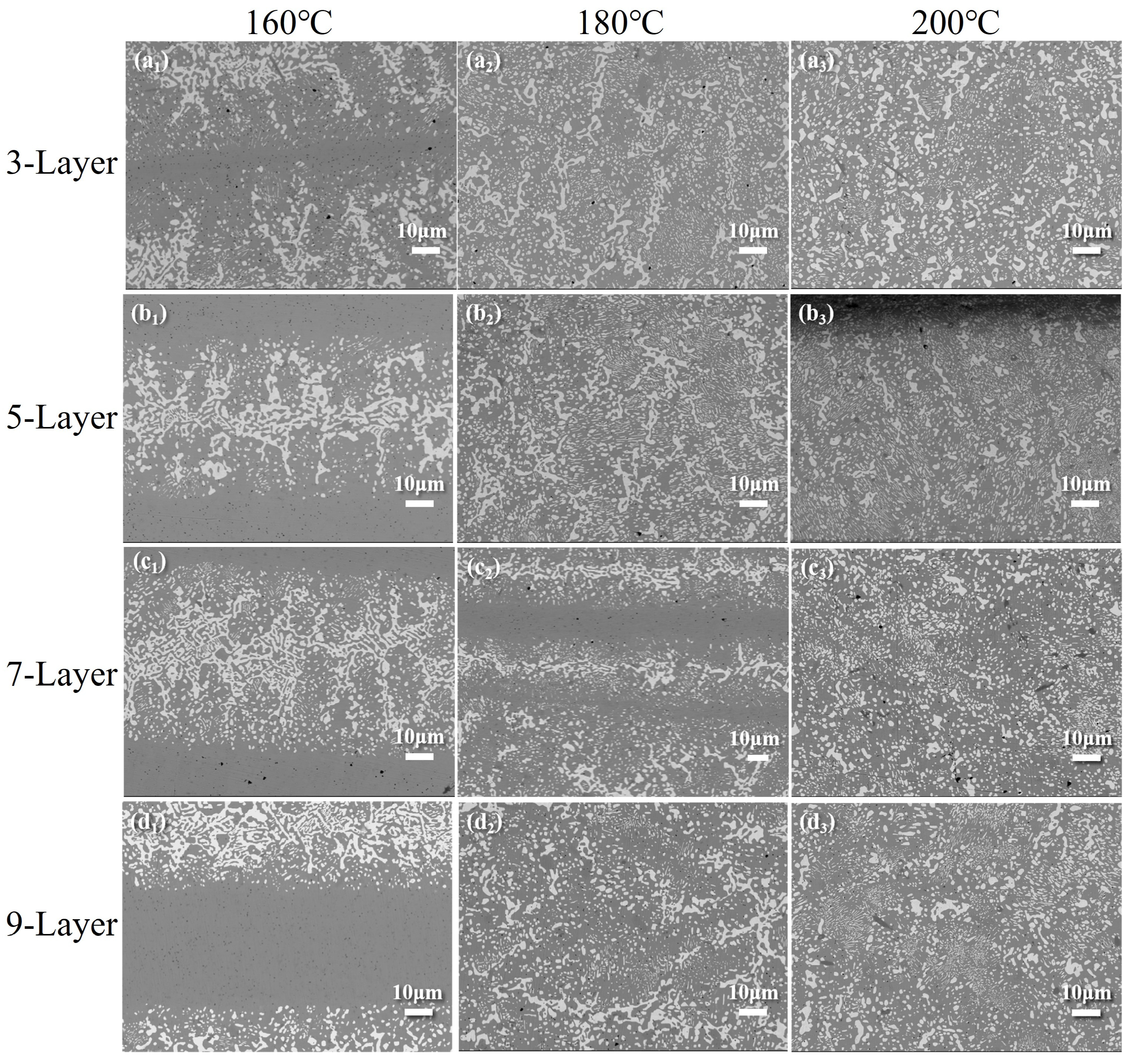
3.3.2. Interface Structure and Bi-Rich Phase Distribution After Soldering
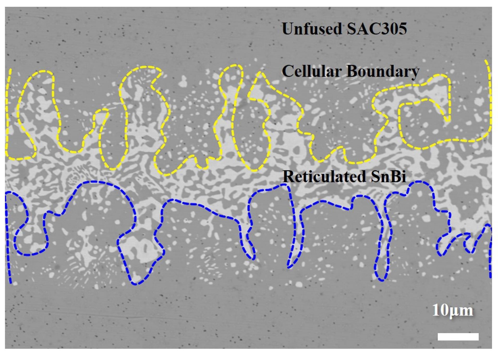
As shown in Figure 10 (a1–d1), after soldering at 160 °C, the junction between the SnBi layer and the SnAgCu layer exhibited a cellular structure, with Bi-rich particles diffusely distributed along the cellular boundary. In the 7- and 9-layer solders, the part of the SnBi layer away from the SnAgCu region retained its reticulated organization, showing fishbone-like distribution characteristics. In contrast, the 3- and 5-layer solders, due to a greater degree of fusion of the SnAgCu layer, show that the internal parts of the top and bottom SnBi layers (away from the SnAgCu region) contain more β-Sn phases, forming a sub-eutectic structure.
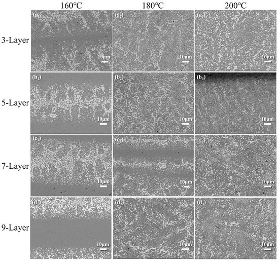
Figure 10.
Backscattered images of Bi-rich phase distribution in the cross-section of layered composite solder/Cu after soldering at different temperatures: (a1,a2,a3) 3-layer, (b1,b2,b3) 5-layer, (c1,c2,c3) 7-layer, (d1,d2,d3) 9-layer.
In summary, the cross-sectional microstructure can be categorized into the characteristic regions of “unfused SAC305 zone + cellular boundary zone + reticulated SnBi zone” (Figure 11). These results can be further explained by considering the interfacial metallurgical principles derived from the synchrotron radiation experiments. During the reflow process, the SnBi layer melts and wets both the SnAgCu layer and the Cu substrate. Interfacial metallurgical reactions occur at the SnAgCu/SnBi junction, where the SnAgCu layer partially dissolves until the molten solder material reaches a sub-eutectic equilibrium. The Bi contents of the 3-, 5-, 7-, and 9-layer solder were 34.8%, 30.6%, 29.0%, and 28.1%, respectively. At 160 °C, the higher Bi content increases the liquid-phase/solid-phase ratio, leading to a higher dissolution of SnAgCu in the 3- and 5-layer solders and resulting in more significant fusion. Once the liquid-phase region expands, the solid–liquid interface fronts solidify due to the supercooling of the components, forming a cellular interface. This cellular interface is mainly composed of Bi-rich particles, β-Sn phase, Ag3Sn particles, and a small amount of Cu6Sn5 particles.

Figure 11.
Layered composite solder cross-section zoning.
During cooling, the β-Sn phase precipitates first. As the temperature drops to the eutectic point, the remaining liquid phase transforms into a reticulated Sn58Bi eutectic structure. When the temperature is further lowered, Bi precipitates from the β-Sn phase to form reticulated and granular Bi-rich particles. For the undissolved SAC305 layer, the Ag3Sn phase and the β-Sn phase are uniformly distributed, maintaining a complete structure.
At a soldering temperature of 180 °C (Figure 10(c2,d2)), the SnBi/SnAgCu junction still retains a cellular structure, but the Bi-rich particles are more dispersed, and the size of the reticulated Bi phase is significantly reduced. This is due to the increased dissolution of the SnAgCu alloy, enhancing the “dilution” effect of the Bi phase.
After soldering at 200 °C (Figure 10(c3,d3)), the sub-eutectic structure becomes finer compared to the structure after soldering at 180 °C. The Bi particles in the 3-layer and 5-layer solders become finer and more dispersed. Diffuse Ag3Sn and Cu6Sn5 particles are observed in the 3-, 5-, 7-, and 9-layer solder, and the distribution of these particles becomes more uniform with an enhanced refining effect as the temperature increases.
3.3.3. Changes in Interface IMC with Soldering Temperature
The interface IMC and the organization above it, obtained after reflowing 3-, 5-, 7-, and 9-layer composite solder with Cu substrate at different temperatures, were observed and analyzed using EPMA. The results are shown in Figure 12.

Figure 12.
IMC backscattering images of the interface after soldering at different temperatures of the solder joints: (a1,a2,a3) 3-layer, (b1,b2,b3) 5-layer, (c1,c2,c3) 7-layer, (d1,d2,d3) 9-layer.
At a soldering temperature of 160 °C, a scalloped Cu6Sn5 structure is formed at the interface, which aligns with the known interfacial energy theory [21]. The interfacial energy between the liquid solder and intermetallic compounds is significantly lower than that between solid solder and intermetallic compounds. Consequently, the Cu6Sn5 interfacial intermetallic compounds formed by the molten solder during reflow tend to adopt a scallop-shaped morphology, following the principle of energy minimization. The morphology of the IMCs formed at different temperatures is similar to that of scallop shapes. Additionally, a large concentration of Bi is found at the “solder/IMC” interface. This is because, during the reflow process, the liquid solder reacts with the Cu substrate to form Cu6Sn5, consuming a significant amount of Sn. This results in an increase in Bi concentration near the IMC. Since Bi does not participate in the formation of Cu6Sn5, it continues to migrate into the solder joints, forming a significant Bi accumulation. The dissolution of Sn in the SAC305 layer can dilute the Bi concentration in the solder joints. However, since the reflow temperature is low at 160 °C, the dissolution of SAC305 into the liquid solder is limited, and the solder remains close to the eutectic composition, resulting in the formation of a mesh eutectic structure upon cooling. Moreover, the Ag and Cu elements in the SAC305 layer have barely diffused to the interface between the solder and the Cu substrate, and the Ag3Sn phase is almost absent at the solder joint interface.
When the temperature increases to 180 °C, the dissolution of SAC305 increases, which, on the one hand, dilutes the Bi concentration in the underlying solder and, on the other hand, promotes the diffusion of more Ag and Cu atoms into the solder. This results in the generation of Ag3Sn and Cu6Sn5, which, to some extent, contribute to grain refinement. The continuous lamellar Bi phase gradually transforms into finer, dispersed particles. In the 3-layer and 5-layer solders, larger Ag3Sn particles were distributed above the interface IMC, while in the 7-layer and 9-layer solders, the Bi phase dominated above the IMC and in the interstitial space. The Ag content was lower due to the incomplete dissolution of the SAC305 layer.
At a soldering temperature of 200 °C, the Bi phase above the interface IMC becomes more dispersed. In the 7-layer and 9-layer solder joints, more Ag3Sn particles are distributed above the IMC, while in the 3-layer and 5-layer solders, the Ag3Sn particles become finer and more uniformly distributed. The increase in temperature induces more complete diffusion of Ag atoms and suppresses Bi aggregation.
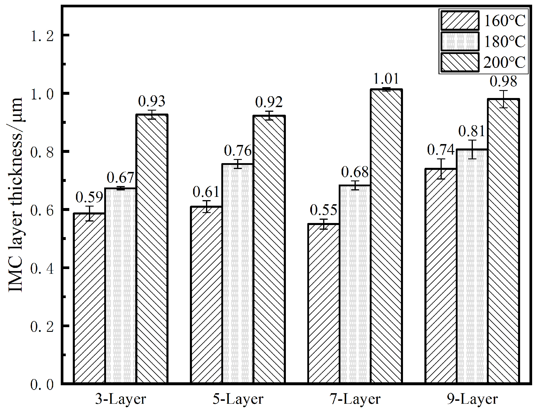
The total area of IMCs was calculated by linearly selecting EBSD images using Photoshop software (v 26.2.0), and the IMC thickness was obtained by dividing the total area by the interface length. The IMC layer thicknesses for the four solder joints at different temperatures are shown in Figure 13. The IMC thickness increases with temperature, especially at 200 °C, where the growth rate is significant. The growth rate of interfacial IMC is influenced by the interfacial reaction rate and the Cu atom supply rate. It has been shown that the nano-width liquid channels between different Cu6Sn5 grains serve as the main path for Cu atoms to diffuse to the IMC front in micro-solder joint reflow [19]. Higher temperatures accelerate the dissolution rate of Cu atoms from the Cu substrate into the liquid solder. When the Cu content becomes oversaturated, the Cu reacts with Sn to form IMC, and the higher temperature also accelerates the interfacial reaction rate, causing the IMC growth to speed up as the temperature increases.
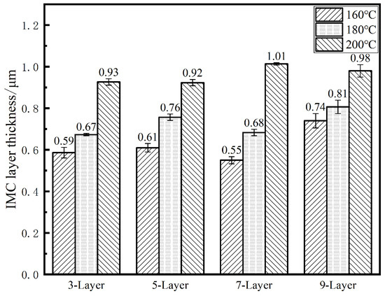
Figure 13.
Variation in IMC thickness at the interface of 3-, 5-, 7-, and 9-layer solder joints under different soldering temperatures.
The thickness of IMC at the interface of the solder joints for different layers at the same temperature does not vary significantly, indicating that the number of layers has little effect on IMC growth at the interface. This is because the interfacial reaction primarily occurs between the bottom solder and the Cu substrate, and the bottom solder in all layers is Sn58Bi. Thus, the number of layers has a minimal impact on the IMC thickness at the interface.
3.4. Shear Properties of Layered Composite Solder Joints
3.4.1. Shear Strength
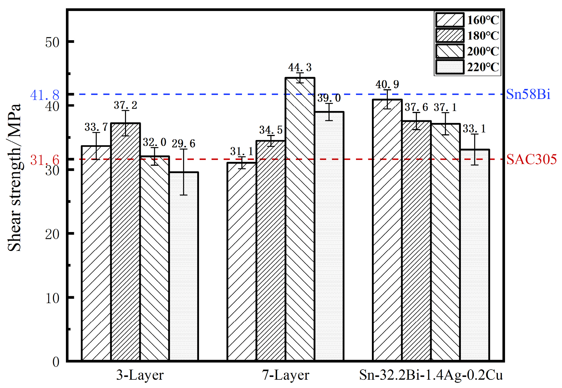
Figure 14 illustrates the shear strength of Cu/solder/Cu joints after reflow of 3-layer composite solder and 7-layer composite melt-cast state solder at different temperatures. For comparison, the shear strengths of Cu/Sn58Bi/Cu joints after reflow at 180 °C and Cu/SAC305/Cu joints after reflow at 250 °C were also tested, with values of 41.8 ± 1.1 MPa and 31.6 ± 1.4 MPa, respectively.
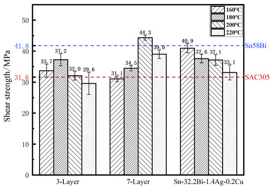
Figure 14.
Shear strength of joints at different reflow temperatures.
The shear strength is concurrently determined by the intermetallic compound (IMC) at the interface and the microstructure of the solder. As is evident from Section 3.3.3, subsequent to reflow at the identical temperature, the morphology and thickness of the IMC in solders with varying numbers of layers exhibit fundamental similarity. Nevertheless, upon reflow at a given temperature, conspicuous disparities exist in the shear strength of the solder joints of the 3-layer and 7-layer composite solders, attributable to the dissimilarities in their internal microstructures.
The complete mixing temperatures of the 3-layer and 7-layer composite solders are 172 °C and 181 °C, respectively.
After reflow at 160 °C, the IMCs in both the 3-layer and 7-layer composite solder joints are relatively thin, which constitutes the primary cause of their low shear strength. At this temperature, both the 3-layer and 7-layer composite solders maintain their layered structures. However, the 7-layer composite solder features a lower degree of fusion and a greater number of interfaces. Consequently, its shear strength is marginally lower than that of the 3-layer composite solder. The intensity difference on either side of the SnBi-SAC interface is remarkable, rendering this region a vulnerable site where cracks are prone to initiate and propagate. The shear strength of the melt-cast Sn-32.2Bi-1.4Ag-0.2Cu solder, following reflow at 160 °C, amounts to 40.9 ± 1.5 MPa, surpassing that of the 3-layer and 7-layer composite solders. During the reflow process, the composition of the outermost layer of the layered composite solder approximates that of Sn58Bi, whereas the Sn content in the melt-cast solder is substantially higher than that in Sn58Bi, thereby facilitating a more rapid growth of Cu6Sn5. Hence, the melt-cast solder possesses a higher shear strength.
After reflow at 180 °C, the 3-layer composite solder has undergone complete mixing. Its homogeneous microstructure and appropriately thick IMC enables its shear strength to reach a peak value. Conversely, the 7-layer composite solder still retains its layered structure. The presence of interfaces and a more heterogeneous microstructure result in the shear strength of the 7-layer composite solder being slightly lower than that of the 3-layer composite solder.
After reflow at 200 °C, the shear strength of the 7-layer composite solder registers at 44.3 ± 0.8 MPa. This represents the maximum shear strength within this series of experiments and is the sole value exceeding the shear strength of Sn58Bi. Prior to reflow, the 7-layer composite solder preserves its layered structure, with the composition of the outermost layer being similar to that of Sn58Bi. The growth of the IMC at the Cu–pad interface also exhibits resemblance. Its distinct feature lies in the fact that, under this condition, the SAC305 solder is completely dissolved and uniformly dispersed within the SnBi layer. The uniformly dispersed Bi-rich phase and Ag3Sn can exert a second-phase strengthening effect, causing the microstructure of the solder joints to be the most refined and homogeneous under this condition, thereby attaining the maximum shear strength.
3.4.2. Fracture Morphology
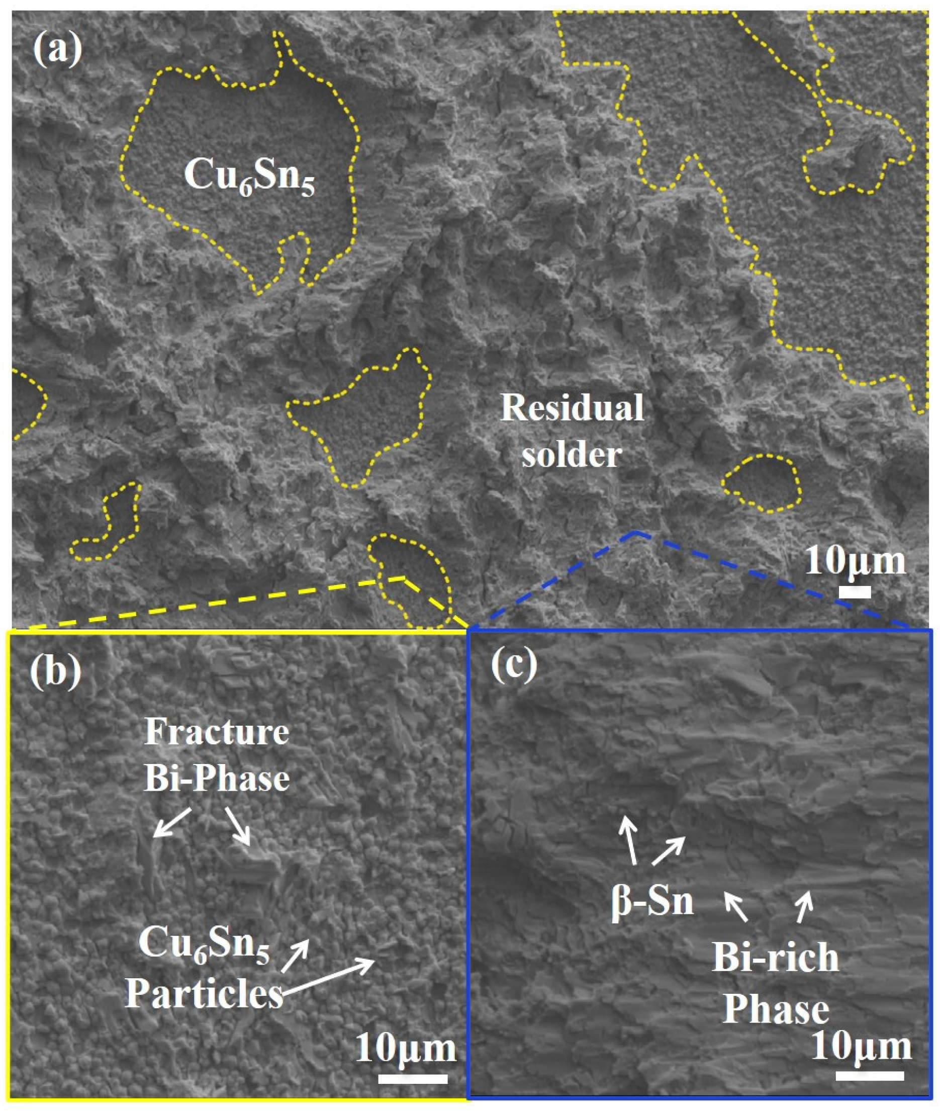
According to the existing literature [22,23] and the laminar structural properties of the braze material in this study, the joints may undergo the following fracture modes during shear: interfacial IMC fracture, IMC/solder interfacial fracture, intra-solder material fracture, and SnBi/SAC interfacial fracture. Experimental observations revealed that solder residues and Cu6Sn5 (or craters left by Cu6Sn5 embedded in the solder) were visible on all the fractures, indicating that the fracture mainly occurred at the solder and IMC/solder interfaces. All the fractures exhibited a mixed plastic/brittle fracture mode. Due to differences in soldering temperature, solder structure, and composition, the percentage of different fracture modes varied. Specific fracture characteristics are outlined below.
As shown in Figure 15, the joint fracture of the 3-layer composite solder reflowed at 160 °C is characterized by incomplete fusion of the SnBi and SnAgCu solders. Due to the varying degrees of deformation of these two solders under the same shear load, the SnBi/SAC interface becomes the weak link of the joint, resulting in fracture occurring at this interface, which exposes the SnAgCu in the interlayer (Figure 16). Due to the low reflow temperature, there is less Cu6Sn5 at the interface at the fracture, and smooth Cu surfaces are exposed in some areas. As the reflow temperature increases, the amount of interfacial Cu6Sn5 increases, and the IMC interfacial strength improves. However, the excessive thickness of Cu6Sn5, a hard and brittle phase, leads to the degradation of joint performance. Consequently, the proportion of fractures occurring at the IMC/solder interface increases at 200 °C and 220 °C, resulting in a corresponding decrease in shear strength.
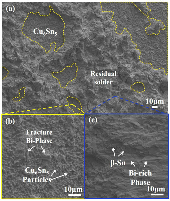
Figure 15.
Fracture morphology of solder joints: (a) fracture morphology, (b) fracture at the IMC/solder interface, (c) fracture within the solder material.

Figure 16.
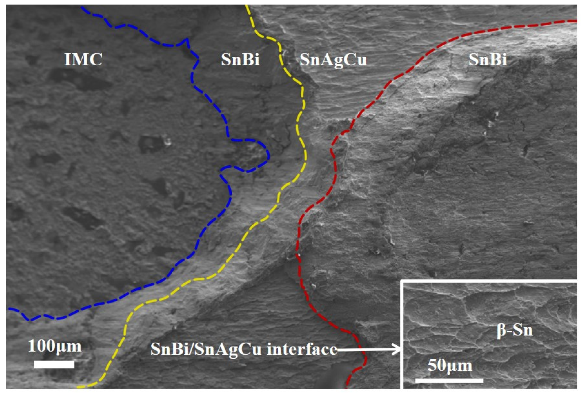
Fracture morphology of 3-layer composite solder SnBi/SnAgCu without complete fusion.
The fracture characteristics of the 7-layer composite solder follow the same temperature-dependent pattern as those of the 3-layer composite solder. However, due to its higher complete fusion temperature, fractures occurring at the SnBi/SAC interface can still be observed in fractures at 160 °C and 180 °C. Once the reflow temperature exceeds 180 °C, the SnBi/SAC interface disappears, and fracture occurs throughout the solder. For the melt-cast Sn-32.2Bi-1.4Ag-0.2Cu alloy, the fracture modes predominantly occurred within the braze and at the IMC/solder interface, with the IMC/solder interface fracture being dominant.
4. Conclusions
This study systematically investigates the Sn58Bi/SAC305 layered composite solder, focusing on its microstructural evolution and interfacial dynamics during low-temperature soldering. The key findings are summarized as follows:
- (1)
- The alternating layers of SAC305 and Sn58Bi enable controlled element diffusion during reflow. Bi diffusion into SAC305 reduces segregation, while the partial dissolution of SAC305 into molten Sn58Bi forms a sub-eutectic structure. Synchrotron imaging reveals that cellular interfaces arise from compositional supercooling, driven by localized Bi enrichment and rapid solidification at the solid–liquid boundary.
- (2)
- The fusion degree of layered solder increases with temperature, transitioning from a partially mixed “unfused SAC305 zone + cellular boundary zone + reticulated SnBi zone” (160–180 °C) to a fully homogenized structure (200 °C). The refined distribution of Ag3Sn and Cu6Sn5 phases at elevated temperatures enhances grain boundary strengthening, while excessive IMC growth at 220 °C degrades joint reliability.
- (3)
- Although melt-cast solders perform well at lower temperatures, the 7-layer composite solder reaches a peak shear strength of 44.3 ± 0.8 MPa at 200 °C, slightly surpassing Sn58Bi (41.8 ± 1.1 MPa). This is due to its uniform phase dispersion and optimized IMC thickness, making it suitable for applications that require both low-temperature assembly and high-temperature reliability. Fracture analysis indicates mixed ductile–brittle modes, with crack initiation predominantly at solder/IMC interfaces or heterogeneous layer boundaries.
This work demonstrates that layered architectures can regulate element redistribution and interfacial reactions, offering a strategy to balance low-temperature processability and mechanical performance. Future studies should explore layer-count optimization and interfacial alloying to further suppress Bi brittleness and IMC overgrowth.
Author Contributions
Conceptualization, Z.Z. and D.Z.; methodology, Z.Z. and D.Z.; software, W.Y. and C.L.; validation, Z.Z., D.Z. and Y.W.; formal analysis, Z.Z. and D.Z.; investigation, W.Y. and C.L.; resources, H.M. (Haoran Ma) and H.M. (Haitao Ma); data curation, D.Z., C.L. and W.Y.; writing—original draft preparation, Z.Z.; writing—review and editing, H.M. (Haitao Ma), Y.W. and H.M. (Haoran Ma); supervision, H.M. (Haoran Ma) and H.M. (Haitao Ma); project administration, H.M. (Haoran Ma) and Y.W.; funding acquisition, H.M. (Haoran Ma) and H.M. (Haitao Ma). All authors have read and agreed to the published version of the manuscript.
Funding
This research received no external funding.
Data Availability Statement
The original contributions presented in this study are included in the article. Further inquiries can be directed to the corresponding author.
Acknowledgments
We thank the Shanghai Synchrotron Radiation Facility for its technical support during our research.
Conflicts of Interest
The authors declare no conflicts of interest.
References
- Ma, Y.; Li, X.; Yang, L.; Zhou, W.; Wang, M.; Zhu, W.; Wu, P. Effects of graphene nanosheets addition on microstructure and mechanical properties of SnBi solder alloys during solid-state aging. Mater. Sci. Eng. A 2017, 696, 437–444. [Google Scholar] [CrossRef]
- Suganuma, K. Advances in lead-free electronics soldering. Curr. Opin. Solid State Mater. Sci. 2001, 5, 55–64. [Google Scholar] [CrossRef]
- Sidhu, R.; Chawla, N. Microstructure Characterization and Creep Behavior of Pb-Free Sn-Rich Solder Alloys: Part I. Microstructure Characterization of Bulk Solder and Solder/Copper Joints. Metall. Mater. Trans. A 2008, 39, 340–348. [Google Scholar] [CrossRef]
- Keller, J.; Baither, D.; Wilke, U.; Schmitz, G. Mechanical properties of Pb-free SnAg solder joints. Acta Mater. 2011, 59, 2731–2741. [Google Scholar] [CrossRef]
- Prabhu, K.N.; Deshapande, P.; Satyanarayan. Effect of cooling rate during solidification of Sn–9Zn lead-free solder alloy on its microstructure, tensile strength and ductile–brittle transition temperature. Mater. Sci. Eng. A 2012, 533, 64–70. [Google Scholar] [CrossRef]
- Yagi, S.; Ichitsubo, T.; Matsubara, E.; Yamaguchi, M.; Kimura, H.; Sasamori, K. Interfacial reaction of gas-atomized Sn-Zn solder containing Ni and Cu additives. J. Alloys Compd. 2009, 484, 185–189. [Google Scholar] [CrossRef]
- Yang, W.; Mao, J.; Ma, Y.; Yu, S.; He, H.; Qi, D.; Zhan, Y. Effects of yttrium addition on the microstructure evolution and electrochemical corrosion of Sn–9Zn lead-free solders alloy. Materials 2021, 14, 2549. [Google Scholar] [CrossRef]
- Sundelin, J.J.; Nurmi, S.T.; Lepistö, T.K.; Ristolainen, E.O. Mechanical and microstructural properties of SnAgCu solder joints. Mater. Sci. Eng. A 2006, 420, 55–62. [Google Scholar] [CrossRef]
- Huang, X.; Wang, Z.; Yu, Y. Thermomechanical properties and fatigue life evaluation of SnAgCu solder joints for microelectronic power module application. J. Mater. Res. Technol. 2020, 9, 5955–5967. [Google Scholar] [CrossRef]
- Zhang, H.; Xu, Z.; Wang, Y.; Tian, C.; Fan, C.; Motozuka, S.; Yu, J. The Effect of Bi Addition on the Electromigration Properties of Sn-3.0Ag-0.5Cu Lead-Free Solder. Metals 2024, 14, 1149. [Google Scholar] [CrossRef]
- Wang, F.; Chen, H.; Huang, Y.; Liu, L.; Zhang, Z. Recent progress on the development of Sn–Bi based low-temperature Pb-free solders. J. Mater. Sci. Mater. Electron. 2019, 30, 3222–3243. [Google Scholar] [CrossRef]
- Wang, X.; Zhang, L.; Li, M.L.; Wang, X.; Zhao, M. Enhancement of structure and properties of Sn58Bi solder by AlN ceramic particles. J. Mater. Sci. Mater. Electron. 2022, 19, 2584–2595. [Google Scholar] [CrossRef]
- Chen, L.T.; Chen, C.M. Electromigration study in the eutectic SnBi solder joint on the Ni/Au metallization. J. Mater. Res. 2006, 21, 15–21. [Google Scholar] [CrossRef]
- Liu, Y.; Fu, H.; Sun, F.; Zhang, H.; Kong, X.; Xin, T. Microstructure and mechanical properties of as-reflowed Sn58Bi composite solder pastes. J. Mater. Process. Technol. 2016, 238, 290–296. [Google Scholar] [CrossRef]
- Ye, D.; Du, C.; Wu, M.; Lai, Z. Microstructure and mechanical properties of Sn–xBi solder alloy. J. Mater. Sci. Mater. Electron. 2015, 26, 3629–3637. [Google Scholar] [CrossRef]
- Fan, Y.; Zhang, K.; Chen, W.; Wu, J.; Wang, Y. Thermomigration Microstructure and Properties of Ni Nanoparticle-Reinforced Sn58Bi Composite Solder/Cu Solder Joint. Metals 2024, 14, 1420. [Google Scholar] [CrossRef]
- Ren, G.; Collins, M.N. Improved reliability and mechanical performance of Ag microalloyed Sn58Bi solder alloys. Metals 2019, 9, 462. [Google Scholar] [CrossRef]
- Zhang, P.; Xue, S.; Wang, J. New challenges of miniaturization of electronic devices: Electromigration and thermomigration in lead-free solder joints. Mater. Des. 2020, 192, 108726. [Google Scholar] [CrossRef]
- El-Daly, A.A.; El-Taher, A.M.; Gouda, S. Development of new multicomponent Sn–Ag–Cu–Bi lead-free solders for low-cost commercial electronic assembly. J. Alloys Compd. 2015, 627, 268–275. [Google Scholar] [CrossRef]
- Wu, X.; Sun, L.; Liu, Y.; Ye, Z.; Zhao, X.; Liu, Y. Preparation and performance of Sn-based composite solder joints by solid-liquid low-temperature solder bonding technology. J. Mater. Res. Technol. 2023, 24, 6378–6390. [Google Scholar] [CrossRef]
- Suh, J.; Tu, K.; Lutsenko, G.; Gusak, A. Size distribution and morphology of Cu6Sn5 scallops in wetting reaction between molten solder and copper. Acta Mater. 2008, 56, 1075–1083. [Google Scholar] [CrossRef]
- Xu, R.; Liu, Y.; Sun, F. Effect of isothermal aging on the microstructure, shear behavior and hardness of the Sn58Bi/Sn3.0Ag0.5Cu/Cu solder joints. Results Phys. 2019, 15, 102701. [Google Scholar] [CrossRef]
- Zhang, S.; Jing, X.; Chen, J.; Paik, K.; He, P.; Zhang, S. Preparation, characterization and mechanical properties analysis of SAC305-SnBi-Co hybrid solder joints for package-on-package technology. Mater. Charact. 2024, 208, 113624. [Google Scholar] [CrossRef]

Disclaimer/Publisher’s Note: The statements, opinions and data contained in all publications are solely those of the individual author(s) and contributor(s) and not of MDPI and/or the editor(s). MDPI and/or the editor(s) disclaim responsibility for any injury to people or property resulting from any ideas, methods, instructions or products referred to in the content. |
© 2025 by the authors. Licensee MDPI, Basel, Switzerland. This article is an open access article distributed under the terms and conditions of the Creative Commons Attribution (CC BY) license (https://creativecommons.org/licenses/by/4.0/).