Review

Powder Bed Fabrication of Copper: A Comprehensive Literature Review

1
School for Engineering of Matter, Transport and Energy (SEMTE), Arizona State University, Tempe, AZ 85287, USA
2
Fraunhofer Institute for Material and Beam Technology IWS, 01277 Dresden, Germany
3
Commonwealth Scientific and Industrial Research Organization (CSIRO), Clayton, VIC 3168, Australia
*
Authors to whom correspondence should be addressed.
Metals 2025, 15(10), 1114; https://doi.org/10.3390/met15101114
Submission received: 4 August 2025 / Revised: 20 September 2025 / Accepted: 23 September 2025 / Published: 8 October 2025
(This article belongs to the Section Additive Manufacturing)

Abstract

Powder bed fusion of copper has been extensively investigated using both laser-based (PBF-LB/M) and electron beam-based (PBF-EB/M) additive manufacturing technologies. Each technique offers unique benefits as well as specific limitations. Near-infrared (NIR) laser-based LPBF is widely accessible; however, the high reflectivity of copper limits energy absorption, thereby resulting in a narrow processing window. Although optimized parameters can yield relative densities above 97%, issues such as keyhole porosity, incomplete melting, and anisotropy remain concerns. Green lasers, with higher absorptivity in copper, offer broader process windows and enable more consistent fabrication of high-density parts with superior electrical conductivity, often reaching or exceeding 99% relative density and 100% International Annealed Copper Standard (IACS). Mechanical properties, including tensile and yield strength, are also improved, though challenges remain in surface finish and geometrical resolution. In contrast, Electron Beam Powder Bed Fusion (EB-PBF) uses high-energy electron beams in a vacuum, eliminating oxidation and leveraging copper’s high conductivity to achieve high energy absorption at lower volumetric energy densities (~80 J/mm3). This results in consistently high relative densities (>99.5%) and excellent electrical and thermal conductivity, with additional benefits including faster scanning speeds and in situ monitoring capabilities. However, EB-PBF faces its own limitations, such as surface roughness and powder smoking. This paper provides a comprehensive review of the current state of laser-based (PBF-LB/M) and electron beam-based (PBF-EB/M) powder bed fusion processes for the additive manufacturing of copper, summarizing key trends, material properties, and process innovations. Both approaches continue to evolve, with ongoing research aimed at refining these technologies to enable the reliable and efficient additive manufacturing of high-performance copper components.

1. Introduction

Copper plays an integral role in the global economy and various industries due to its unique properties. It is essential to modern infrastructure, electronics, and clean energy systems. Globally, demand is projected to grow by 275–350% between 2010 and 2050, potentially surpassing current reserves and raising sustainability concerns [1]. Energy use for copper production may rise from 0.3% to 2.4% of global energy demand by 2050, driven by declining ore grades and increased primary extraction [1]. By 2024, the Copper Development Association (CDA) estimates that copper generated approximately $160 billion in the U.S. alone, supporting around 400,000 jobs across sectors such as renewable energy, battery storage, automotive, solar energy, and electrical distribution [2].
One of copper’s most valuable attributes is its exceptional electrical conductivity, the highest among non-precious metals [3]. This conductivity stems from its loosely bound valence electrons, which can move freely through the atomic lattice [4]. As a result, copper is widely utilized in electrical wiring, transmission connectors, rotors, and components in microelectronics [5,6,7,8,9,10,11]. Additionally, it plays a critical role in the manufacturing of battery electrodes, particularly for lithium-ion batteries [12]. Its use in conductive inks for flexible electronics enables the development of innovative electronic devices that require lightweight and adaptable materials [13,14,15].
In addition to its electrical properties, copper is also recognized for its excellent thermal conductivity, which stems from the free movement of delocalized electrons within the lattice [16]. Because of this, copper has been used to fabricate radiators and heat exchangers in energy storage systems [17,18,19,20]. It is also a crucial material in the manufacturing of brakes in the automotive industry, since the addition of copper helps reduce overheating [21,22].
Furthermore, copper possesses antimicrobial characteristics, which significantly enhance its utility in various applications, particularly in healthcare settings where infection control is critical. Copper-coated surfaces and copper-infused materials, such as textiles and polymers, provide continuous, broad-spectrum antimicrobial activity, which can significantly reduce bacteria on high-touch surfaces in hospitals, like door handles and toilet seats [23,24,25,26]. Studies indicate that copper coatings on public facilities, such as fitness centers, are also effective in minimizing microbial contamination [27]. Furthermore, copper containers have been shown to eliminate bacteria in drinking water [28,29], and copper is commonly used in wound dressings and medical devices to help prevent infections [30].
Another significant advantage of copper is its natural resistance to corrosion, attributed to a protective Cu2O layer that forms on its surface. This property makes copper a preferred material for plumbing systems and marine applications, including gas and desalination pipelines [31,32,33,34,35,36]. The presence of this protective layer helps maintain the integrity of copper over time, even in harsh environments. Additionally, when exposed to natural weathering, the Cu2O layer reacts with trace atmospheric impurities to develop a green patina, which is not only aesthetically pleasing but also durable, making it suitable for roofing applications [37,38].
Copper components are produced through several manufacturing methods, each with its advantages and limitations. Traditional methods such as machining—which includes turning, milling, and drilling—allow for high precision and customization, making them popular across various industries. However, copper is generally considered difficult to machine due to its high ductility and the significant friction generated between the material and cutting tools [39]. Another widely used method is casting, where molten copper is poured into a mold and solidified into a desired shape [40]. While casting is often one of the most cost-effective manufacturing options [41], it can result in defects such as porosity and shrinkage [42]. Moreover, casting requires mold preparation, which adds time and complexity [43]. In contrast, additive manufacturing has emerged as a modern alternative for fabricating copper parts, offering precision, speed, and material efficiency [44].
Additive manufacturing (AM) has attracted significant attention in recent years due to its advantages over traditional manufacturing methods, including design freedom, reduced waste, customization, and rapid production. AM works by slicing a 3D computer model into layers, each a fraction of a millimeter thick, and then printing the object layer by layer from the bottom up until completion. Additive manufacturing (AM) technologies are generally classified into three categories based on the type of feedstock used: solid-based, liquid-based, and powder-based processes [45]. Solid-based 3D printing uses raw materials in their solid state, such as filament or wire. A common example is the fused deposition method, where a filament feedstock is heated through a nozzle and melted to form the 3D structure. Since the process requires local melting of the material at the nozzle, it is typically limited to materials with low melting temperatures, such as polymers. However, it can also be applied to metallic pastes, in which case a post-processing sintering step may be required to consolidate the material.
Another method that uses solid material as feedstock is wire additive manufacturing (WAM). WAM is a technique that uses solid raw material, usually metal, in the form of a wire, which is heated and melted using a laser, electron beam, or electric arc [46]. The melted wire is then deposited onto the workpiece to form a 3D structure. In Wire Arc Additive Manufacturing (WAAM), an electric current flows through the circuit formed by the wire electrode on one side and the workpiece on the other, creating an arc plasma that melts the wire [47]. Alternatively, the wire can also be melted using a laser beam [47] or an electron beam [48]. This technique is efficient in material usage and has low production costs for the wire, although it typically offers lower accuracy compared to powder-based processes [49].
In most common liquid-based additive manufacturing processes, a light source—typically ultraviolet (UV) light—is used to cure photopolymer resin layer by layer, making this method particularly suitable for resin and other polymer-based materials.
Lastly, the powder-based method creates parts using powder as the raw material. Powder-based processes include powder bed fusion (PBF), binder jetting (BJ), and directed energy deposition (DED) [50,51]. In binder jetting, each layer of the part is created by first spreading a layer of powder, followed by the application of a liquid binding agent using an inkjet printhead to selectively bind the powder according to the desired 2D pattern [52]. BJ parts typically require post-process sintering to consolidate the part and remove the polymer binder from the build. DED uses a focused high-energy source—such as a laser, electron beam, or plasma/electric arc—to create a melt pool on the substrate while simultaneously melting feedstock material, typically in powder or wire form, as it is fed into the pool [53]. While DED enables high deposition rates and is well-suited for large, near-net-shape parts, it generally produces coarser microstructures, lower mechanical strength, and poorer geometric resolution compared to powder bed fusion (PBF) [54,55,56]. For instance, DED-processed components often exhibit lower yield strength and ultimate tensile strength due to slower cooling rates and coarser grains, and they are more susceptible to surface waviness and interlayer defects. In contrast, PBF offers significantly finer microstructures, higher resolution, and superior strength and ductility due to rapid solidification and tight thermal control. Given these advantages—and the fact that PBF has been more extensively studied and optimized for high-performance applications in copper and other metals—this review will focus on powder bed fusion technologies.
Powder bed fusion (PBF) processes are categorized based on the energy source used to selectively fuse regions of a powder bed [57]. The two standardized processes are Laser Powder Bed Fusion (PBF-LB) and Electron Beam Powder Bed Fusion (PBF-EB). In PBF-LB, a laser beam scans and selectively melts regions of a metal powder layer to form dense, solid parts. In PBF-EB, an electron beam performs the same function under vacuum conditions. In both processes, after each layer is fused, the powder bed is lowered, a new layer of powder is spread across the build platform, and the next cross-section is scanned. This layer-by-layer process continues until the part is complete.
Laser powder bed fusion has been studied more extensively in recent years as it allows for more precision and accuracy with a lower power output. However, there are some struggles with application to copper powder, which is a valuable material to produce high-heat/electrical conductivity specialized parts. In LPBF, and because copper is highly conductive, copper LPBF builds experience with higher cooling rates, which leads to potential stress cracking [58]. It also requires much higher volumetric energy density (VED) throughout the process to produce smooth, high-density/low-porosity parts with metallic alloys [59]. This density is often expressed in terms of relative density, the ratio of the measured part density to the theoretical density of fully dense copper. Additionally, high reflectivity of copper—particularly in the infrared range used by early low-power LPBF systems—leads to difficulties with absorption of the laser in this method of AM, leading to incomplete melting and high porosity in manufactured parts that use laser powder bed fusion [59].
If the initial copper powder contains oxide impurities, residual oxygen can lead to the formation of Cu2O precipitates during processing, particularly under high thermal gradients. This results in higher defect densities, including lack of fusion and trapped porosity, compared to other manufacturing techniques [59]. Furthermore, LPBF lacks any in situ powder refinement or deoxidation mechanisms, and successful processing typically requires specialized, high-purity copper powders that are costly and difficult to handle [59].
In PBF, the amount of energy delivered by the system is a crucial factor in determining whether the powder melts completely, resulting in a fully dense part. To achieve full density, the provided energy must be sufficient to fully melt the powder. The energy provided by the laser to each unit volume of material can be characterized by volumetric energy density (VED) as follows:
V E D = P S × H D × L T
where P is the laser power, S is the scanning speed of the laser, HD is the hatching distance, and LT is the layer thickness of the powder bed. Adequate volumetric energy density (VED) is required to fully melt the powder and avoid defects caused by a lack of fusion [60]. Conversely, if the VED is too high, excessive heat can cause the molten metal to evaporate, resulting in voids and porosities known as keyhole effects. Beam speed and power can also create different fluid regimes in the melt pool that potentially promote keyhole effects [61]. Both scenarios compromise the quality of the final product, affecting its density and structural integrity. Besides the parameters related to the PBF equipment, the properties of the powder itself also significantly impact the energy required to melt the powder [62].
The two main thermo-physical properties that influence energy absorption are the absorption coefficient and thermal conductivity. These properties are particularly important for laser PBF, as laser interaction with the material is of an optical nature. Highly conductive powder dissipates the heat quickly from the scanned area, potentially preventing complete melting. Conversely, if the material has a low absorption coefficient in the specific laser frequency domain, most of the laser light will be reflected rather than absorbed, leading to insufficient heat absorption and incomplete melting. Both scenarios can result in a part that lacks full density.
Efforts to understand and optimize the powder bed fusion (PBF) process for pure copper have been extensive, driven by the need to overcome challenges such as low IR laser absorptivity, high thermal conductivity, and oxidation during processing. Given copper’s critical applications in electrical, thermal, and structural components—particularly in sectors requiring precise and complex geometries, such as aerospace and biomedical devices [59,63]—Improving the additive manufacturing of copper parts remains a high priority. This paper provides a comprehensive review of the existing literature on powder bed fusion of copper, with a focus on the relationship between process parameters—such as laser power, scanning speed, hatching distance, and layer thickness—and the resulting part properties, including density, electrical conductivity, thermal conductivity, and mechanical characteristics. Recommendations for best practices to achieve defect-free, high-density copper parts using powder bed fusion are also discussed. The complete list of papers used for data analysis in this review is provided in the Supplementary Materials (Table S1 for LPBF and Table S2 for EB-PBF).

Powder Bed Fusion of Copper

Compared to the electron beam, a laser poses more challenges as an optical source. Since laser light is governed by the principles of optical physics, its absorptivity depends on the material’s interaction with light at specific wavelengths. Parts are typically additively fabricated using an infrared laser (wavelength typically in the range of 1000–1100 nm) in powder bed fusion processes [58]. This presents a problem for the powder bed fusion of copper. Copper has a naturally low absorptivity in the infrared spectrum, meaning that only a small portion of the laser’s energy is absorbed by the material. According to measurements by Domine et al. [64] shown in Figure 1, solid copper absorbs just 5% of infrared light. While copper powder demonstrates slightly better absorption at 33%, this limited absorptivity negatively affects the process’s overall efficiency.
To overcome the absorption limit, higher laser power has been implemented, such as the work by Ikeshoji et al. [68] where laser power of up to 1000 W has been used to produce parts with a relative density of 98%. However, the combination of high laser power and high reflectivity of copper could cause damage to the equipment [69]. Other solutions have been proposed to overcome the challenge associated with the absorptivity at infrared wavelengths. As shown in Figure 1, copper’s absorptivity is much higher at wavelengths of 500 nm and lower. This absorptivity increases significantly to more than 40% for solid copper and around 90% for copper powder [64]. Due to copper’s higher absorptivity at the 500 nm wavelength, there has been a push to develop PBF systems equipped with lasers operating in this range, namely green and blue lasers [70,71]. Domine et al. [64] reported that green lasers, which emit at 515 nm, enable lower laser power while still achieving higher-density copper parts compared to those manufactured with infrared lasers. Similarly, Hori et al. [71] demonstrated that a 200 W blue diode laser emitting at 445 nm wavelength significantly improved melt pool stability and enabled the fabrication of dense copper structures, reaching densities up to 99.1%. Lastly, another strategy to improve infrared laser absorption is to modify the powder surface itself. Jadhav et al. [72] demonstrated that coating copper powder with an oxide layer increased its absorptivity from 32% to 58%, enabling more efficient melting under infrared irradiation. However, this approach alters the chemical composition of the printed part, which may affect its purity and properties depending on the application.
Another challenge in powder bed fusion arises from copper’s high thermal conductivity. The rapid heat dissipation caused by copper’s thermal conductivity leads to strong cooling effects, drawing heat away from the melt pool. This results in melt pool instability, which in turn increases the likelihood of defects forming within the printed part and reduces the density of the printed part [73]. Efforts have been made to mitigate the high thermal conductivity of copper during selective laser melting. One strategy involves using base plates made from materials with lower thermal conductivity than copper, which helps retain heat in the melt pool and reduces the rate at which heat is conducted away. Colopi et al. [74] found that utilizing stainless steel AISI 316L base plates resulted in denser parts compared to those fabricated on copper base plates. Abdelhafiz et al. [75] and Lykov et al. [76] reported that preheating improves melt pool stability and results in higher density and part quality.
Electron beam powder bed fusion (EB-PBF) has been explored as an alternative approach for fabricating pure copper components, addressing some of the challenges associated with laser-based powder bed fusion (LPBF) [77]. Unlike infrared lasers, which suffer from low absorptivity in copper, electron beams interact more efficiently with copper powder, enhancing energy absorption and reducing reflectivity-related issues [77]. Additionally, the vacuum environment in EB-PBF minimizes oxidation, resulting in higher material purity, while the elevated preheat temperatures mitigate residual stresses, reducing the need for post-heat treatments [77]. However, EB-PBF of copper presents challenges related to process stability, dimensional accuracy, and defect formation. The high thermal conductivity of copper leads to significant heat dissipation, causing local thermal gradients that contribute to layer curling, delamination, and keyhole defects [77]. Furthermore, the process has a narrow operating window due to sensitivity to thermal boundary conditions and geometric effects. Compared to LPBF, EB-PBF also exhibits lower dimensional accuracy due to the larger beam size and higher energy input, necessitating extensive post-processing [77]. Additionally, the vacuum setup increases overall processing time and cost, further limiting its scalability for industrial applications. While EB-PBF offers advantages in terms of energy efficiency and oxidation control, its challenges in defect mitigation, geometric precision, and powder recovery highlight the need for further process optimization to enhance its viability for copper fabrication [77].
This paper aims to clarify how process parameters and material characteristics influence the quality of pure copper parts fabricated by powder bed fusion. We review current methods by energy source, examine key strategies for process optimization, outline achieved physical properties, and conclude with a comparative discussion and recommended guidelines.

2. State of the Art: Energy Source for PBF of Copper

As mentioned previously, copper has been fabricated using infrared laser, green laser, and e-beam energy sources. Each of these processes offers its advantages and shortcomings. The state of the art for each energy source is categorized in the next sections. In this review, approximately 27 studies focused on LPBF of copper using near-infrared (NIR) lasers, 14 studies examined green laser LPBF, and 16 studies investigated electron beam powder bed fusion (EB-PBF). Most research has centered on NIR laser systems due to their availability, though green lasers have received growing attention for their improved coupling efficiency with copper. EB-PBF, though less common, offers unique advantages and has been studied for its ability to overcome copper’s high reflectivity and oxidation issues. Many parameters impact the quality of the parts, including laser speed, power, hatching space, layer thickness, and others. However, most studies in the literature focus their analysis on VED. VED is a parameter that can be used as a good representation of the amount of heat delivered to the unit volume of material and is a good representative of several process parameters coupled together.

2.1. Infrared Laser

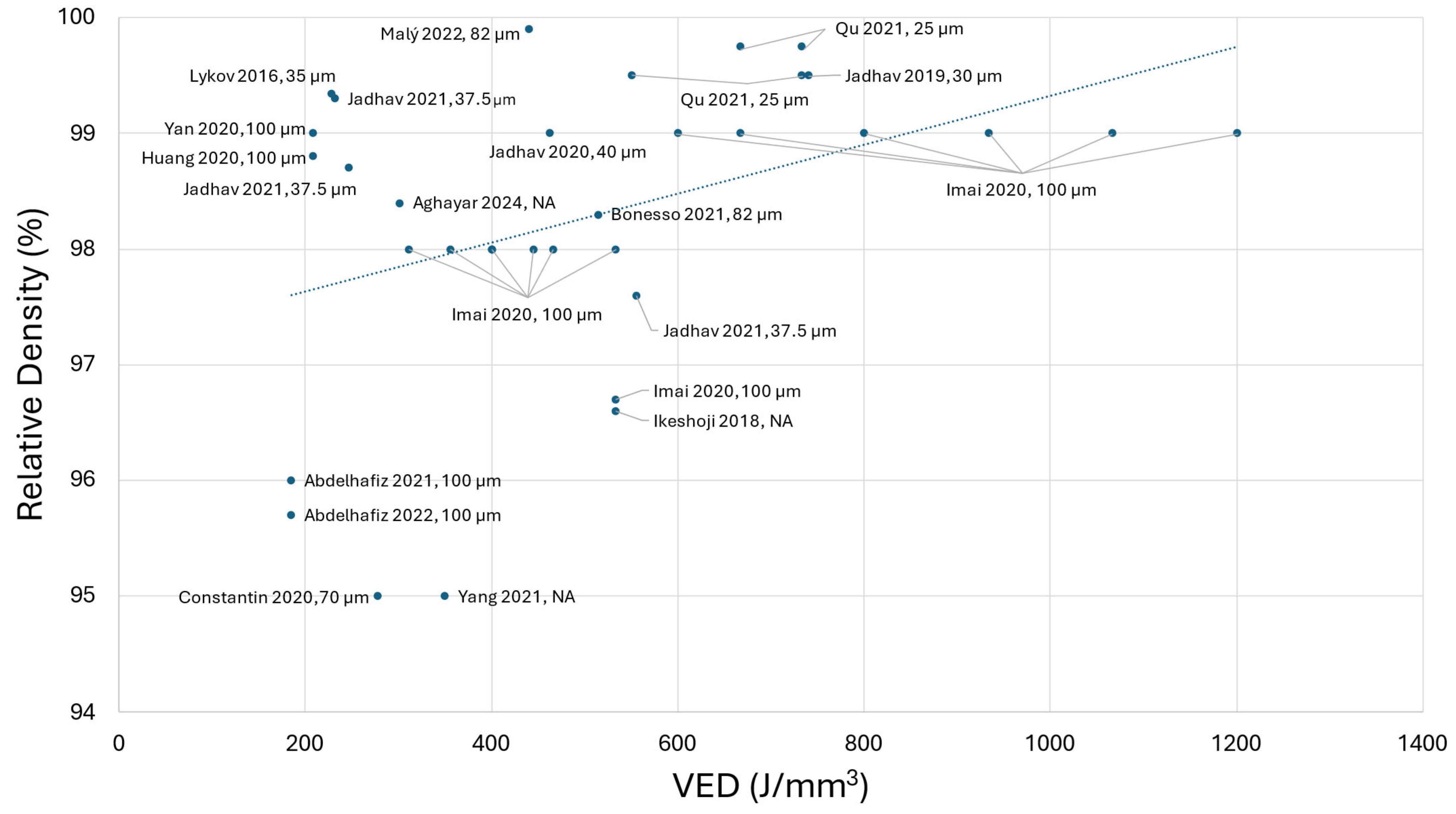
A brief overview of the research papers that conducted powder bed fusion experiments with infrared lasers can be seen in Figure 2. The trend line data shows a weak correlation between the VED and the relative density. Given the scatter in data and lack of data at higher VED values, it is difficult to make a definitive conclusion from the graph. Additional complexity is introduced since each study uses a different machine, which introduces machine and user variability. Additionally, the raw material, particle size distribution, laser spot size, and other factors could potentially impact the final part quality. These factors are clearly not represented in VED and require their own analysis.
Although high relative densities have been achieved across a broad range of VED values (200–1200 J/mm3), higher VEDs generally result in more consistent densification. Nearly all data points above 99% relative density correspond to small laser spot sizes—typically 37.5 µm or less—regardless of VED, likely due to more concentrated energy delivery that promotes efficient melting and consolidation. At lower VEDs (below 400 J/mm3), results are more scattered, but high densities can still be attained with small spot sizes, suggesting that fine focusing can partially compensate for reduced energy input. Conversely, large spot sizes (e.g., 100 µm) are capable of achieving 99% density when combined with sufficiently high VEDs (≥800 J/mm3), indicating that higher energy input can offset the lower energy concentration associated with broader beams.
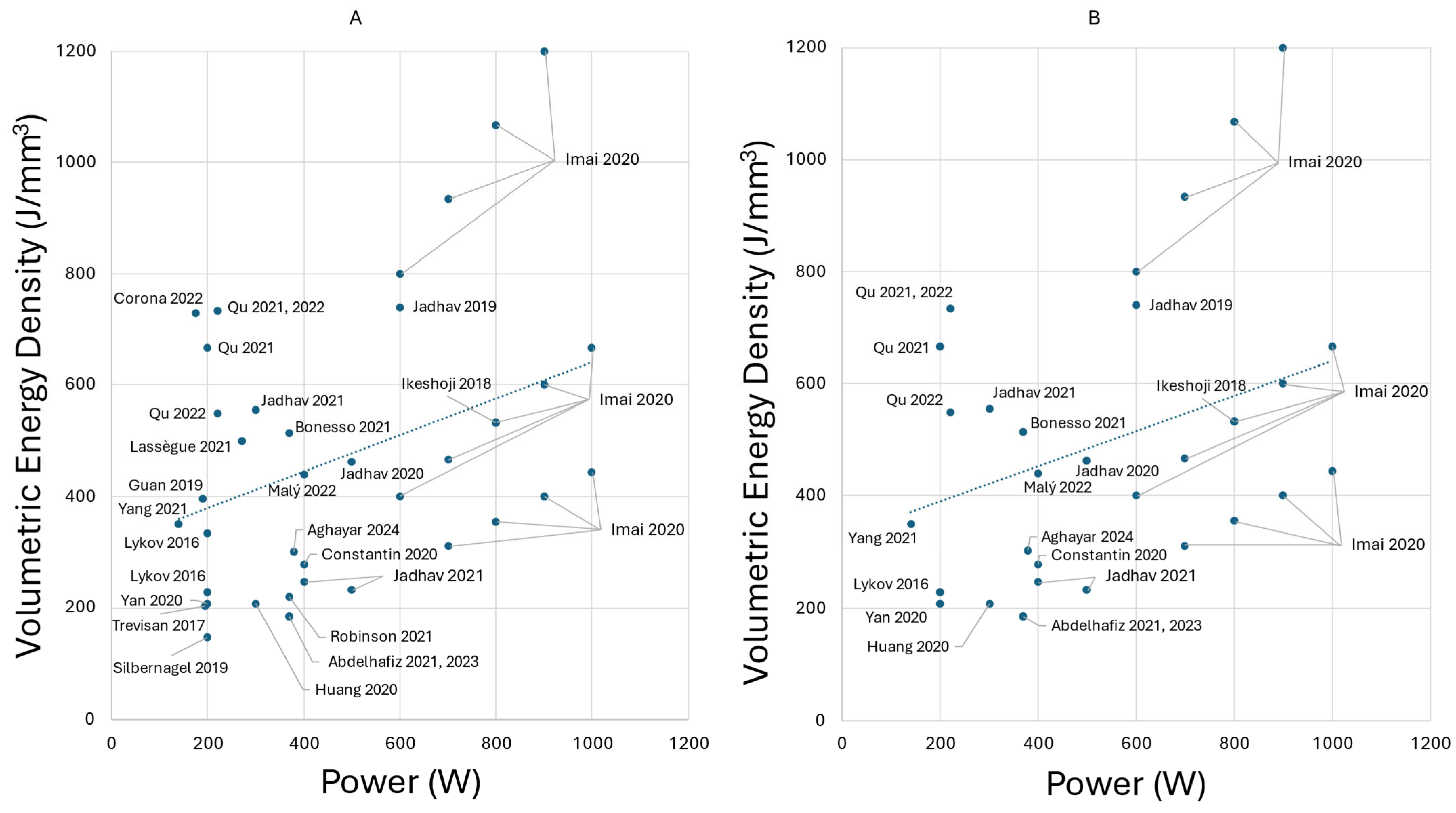
Power is one of the more important parameters, as repeatedly indicated in the literature. Several studies suggested that the power used for copper must be at higher levels for the build to be successful [79,88,89]. However, higher laser powers do not necessarily correspond to higher VED values, as VED is also influenced by scanning speed, hatch distance, and layer thickness, as shown in Equation (1).
Figure 3 shows the relationship between power and the VED used in the literature. The figure also presents the relative density achieved in each study on each data point. As seen in this graph, a wide range of densities has been achieved. Several researchers have used power as low as 200 W. Looking only at this power value, their VED varies over a wide range of values, starting from (150 J/mm3 going all the way to more than 700 J/mm3). One interesting observation is that regardless of the VED used at 200 W power, a wide range of densities is produced. VEDs as small as 200 J/mm3 produced a 99% density in a study conducted by Sharabian et al. [77] and Lykov et al. [76] while VEDs as large as 750 J/mm3 produced a low relative density of 84% as shown by Lassegue et al. [89]. Separating the data for cases with densities higher than 98% as seen in Figure 3B, an interesting trend appears. In this case, the average reported optimal VED of each power level seems to lie within a range of 400 J/mm3 to 600 J/mm3. This range appears especially critical at lower powers (200–400 W), where VEDs below 400 J/mm3 are associated with lower relative densities, while VEDs higher than this consistently produce denser results.
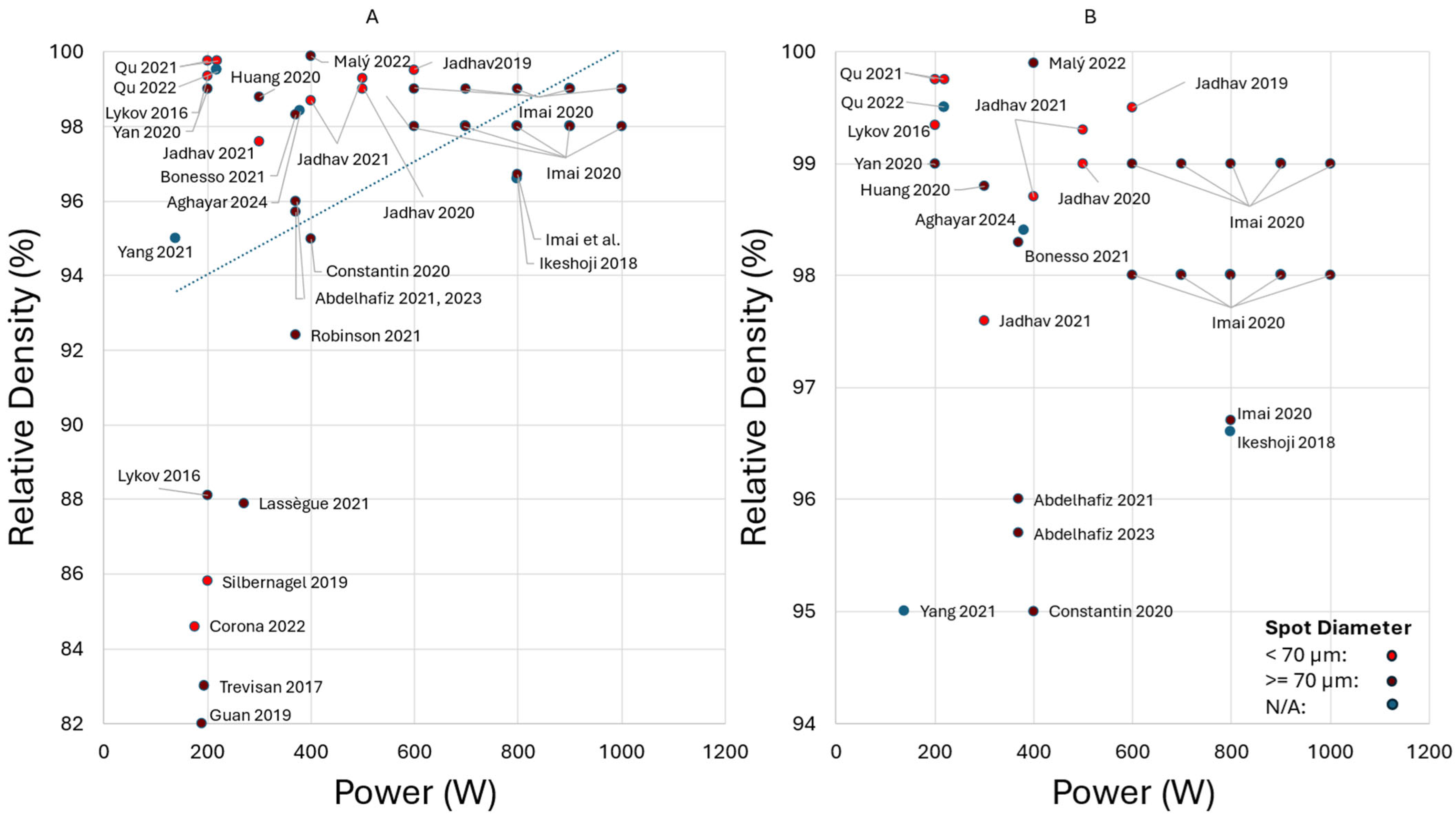
First, even though multiple process parameters contribute to final part density, a closer look at the trend with power, as shown in Figure 4, shows that higher densities than 95% can be achieved across all power values greater than 200 W. Although 200 W generated high-density parts, in some cases, the parts made using 200 W showed lower densities. This indicates that there is an inconsistency between the results at 200 W. It should be noted that for all data points that have achieved a relative density higher than 99%, all [62,76,81] but one [78] used a significantly small beam diameter of 25–35 µm. On the other hand, powers higher than 300 watts consistently created densities higher than 90%. Across the literature, while parts with relatively high densities (>95%) can be fabricated using laser powers ranging from 140 to 1000 watts, achieving highly dense parts at lower powers, such as 200 W, is typically achieved using smaller spot sizes. As can be seen in Figure 4.
Filtering data points that generated densities greater than 98% results in power ranges between 200 watts and 1000 watts, as seen in Figure 4B. It can be seen that relative densities of 98% or higher can be more consistently achieved at power levels above 600 W. It appears that while higher laser power does not necessarily raise the maximum attainable density, it improves the consistency with which high densities are reached. It can also be seen that increasing power above 600 W results in a plateau in relative density. This suggests that although more complete melting can be achieved at higher laser power, overfusion defects are created [79,94], resulting in a plateau in relative density. However, it is important to note that the data on laser power beyond 600 W is only from 2 sources.
A summary of a few cases conducted in the literature with power values less than 200 watts is Table 1. As seen in this table, low powers, regardless of the VED, have shown to produce densities less than 95%. For example, a very high VED (729 J/mm3) used by Corona et al. [91] at 175 W resulted in a density of only 84%, attributing the low relative density to a lack of fusion.
Several studies have shown that increasing laser power generally improves relative density in laser powder bed fusion (LPBF) of copper. Qu et al. [62] and Jadhav et al. [71] observed that higher laser power enhances melt pool formation and interlayer bonding, leading to relative densities as high as 99% in the range of 200–500 W. This improvement is largely attributed to more effective energy absorption and deeper melt pools, especially near the onset of keyhole melting.
However, higher power levels can introduce defects. As power increases beyond ~400 W, issues such as spatter ejection, keyhole porosity, and thermal stresses become more pronounced. These effects are caused by excessive melt pool depth and unstable dynamics, which reduce part density and quality. Ma et al. [88] and Robinson et al. [6] both reported decreased density due to splashing or keyhole formation at higher powers, including cases as low as 370 W.
The highest densities are often achieved just below the threshold for keyhole instability, where energy absorption is maximized without destabilizing the melt pool. However, power alone is not sufficient to guarantee high quality. Copper’s high thermal conductivity increases thermal gradients and residual stresses, especially at high powers, but these effects can be mitigated by preheating the base plate or using lower-conductivity substrates, as shown in prior studies [75,76].
In conclusion, achieving high density in LPBF of copper requires carefully balancing laser power to stay just below the keyhole regime, while managing thermal effects through strategies like base plate preheating.

2.1.1. Process Optimization

Optimizing process parameters in LPBF is essential for achieving high-quality, dense copper parts. While VED is a commonly used metric, studies show that the interaction between laser power, scanning speed, hatch distance, and layer thickness play a more pronounced role than VED values alone. For instance, Imai et al. [85] achieved >99% relative density (RD) at VEDs near 1000 J/mm3, whereas Jadhav et al. [79] reported superior densification at much lower VED (~200 J/mm3), underscoring the importance of parameter relationship over fixed energy input.
Laser power and scanning speed must be carefully balanced to ensure sufficient energy without causing instability. As power increases, faster scan speeds are needed to maintain melt pool stability. Hatch distance significantly affects overlap: while ~100 µm often yields the highest RD [68,75], smaller values can cause rapid cooling and melt pool instability, particularly due to copper’s high thermal conductivity and surface tension effects [68].
Layer thickness shows an inverse relationship with density. Thinner layers allow better melting and energy distribution but may introduce recoat challenges [86]. Although layer thickness can get as low as 10 µm, most studies use 30 µm [69,78,79,84,95] as too thin of a layer thickness can cause powder recoating issues. Scanning strategies also influence melt behavior. Circular and rotated meander paths reduce surface roughness and porosity by improving heat distribution [86,88].
Additional factors such as substrate selection, powder properties, and preheating influence print quality. Finer powders and additives like phosphorus enhance densification and surface finish [82]. Preheating to ~400 °C has shown to reduce energy demand for melting and improve RD, though excessive heating may cause oxidation and powder agglomeration [86]. Remelting strategies can also help resolve the meltpool shrinkage problem that can create cracks [93].
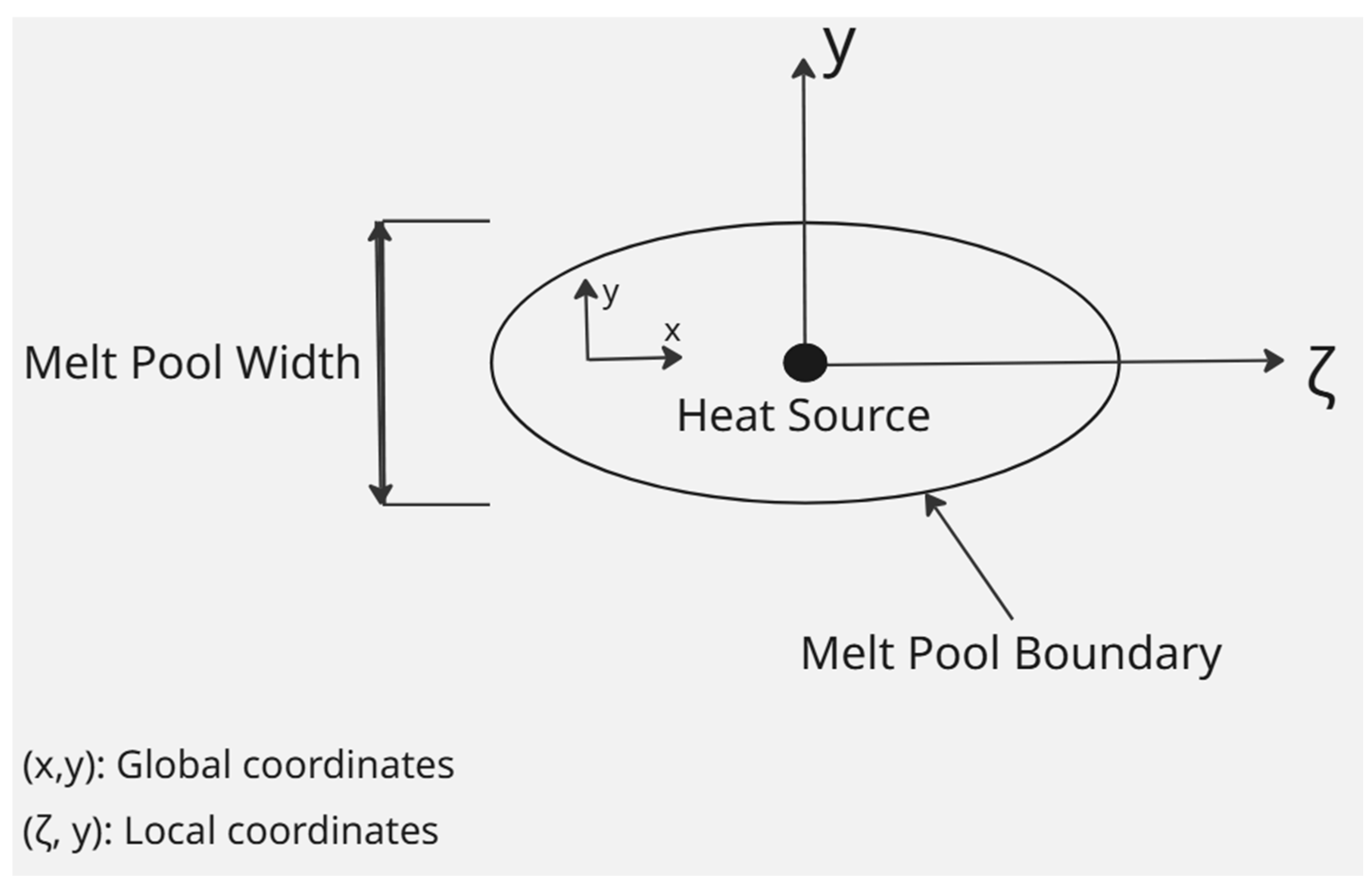
Another theoretical approach for determining the conditions necessary for complete melting is the lack of fusion (LOF) criterion [60,96]. This geometrical method uses Rosenthal’s equation [97] to determine the temperature distribution in a semi-infinite plate heated by a moving point source. A schematic of the melt pool can be shown in Figure 5.
We identify the widest point of the melt pool in the transverse direction by imposing the geometric condition dy/dζ = 0, where y and ζ are the transverse and longitudinal coordinates, respectively, along the melting isotherm. T0
This results in the following system of equations:
T = T 0 + Q 2 π k r e v ( ζ + r ) 2 α
1 + ln N × r = ln N × r r × M  
N = 2 k π ( T m T 0 ) Q ε
M = V 2 α
y = r × 1 + 2 × r × M 1 + r × M
where Tm is the melting temperature of copper, T0 is the ambient temperature of the powder bed, Q is the supplied power, ε is the absorptivity of copper powder, k is the thermal conductivity, V is the scanning speed, ζ distance ahead or behind the moving heat source along the direction of motion, x and y are the global coordinates, r is the distance from the widest point of the melt pool to the heat source, α is the thermal diffusivity, N and M are constants that can be determined by the process parameters. Equation (2) is the Rosenthal solution for a moving point heat source [97]. Equation (3) is derived by setting the temperature equal to the melting point and solving for r, the radial distance (perpendicular to the direction of motion) to the melt pool boundary. Solving Equation (3) numerically yields the value of r, the radial distance from the heat source to the melt boundary at its maximum width. This value is then used in Equation (6) to calculate the melt pool half-width y.
According to the LOF criterion, the melt pool must be large enough to penetrate the current layer and wide enough to overlap adjacent melt pools. This ensures no unmelted powder remains between scan tracks. To satisfy this, the melt pool width must be at least equal to the hatching distance, and the melt pool depth (assumed to be equal to half the width due to symmetry in the y and z directions) must be at least equal to the layer thickness.
Using Rosenthal’s equation, for any given laser power and scanning speed, we can calculate the maximum allowable layer thickness and hatching distance that ensure complete melting. Therefore, the minimum required volumetric energy density (VED) can also be derived. However, this minimum VED is only meaningful if the conditions for hatching distance and layer thickness are met.
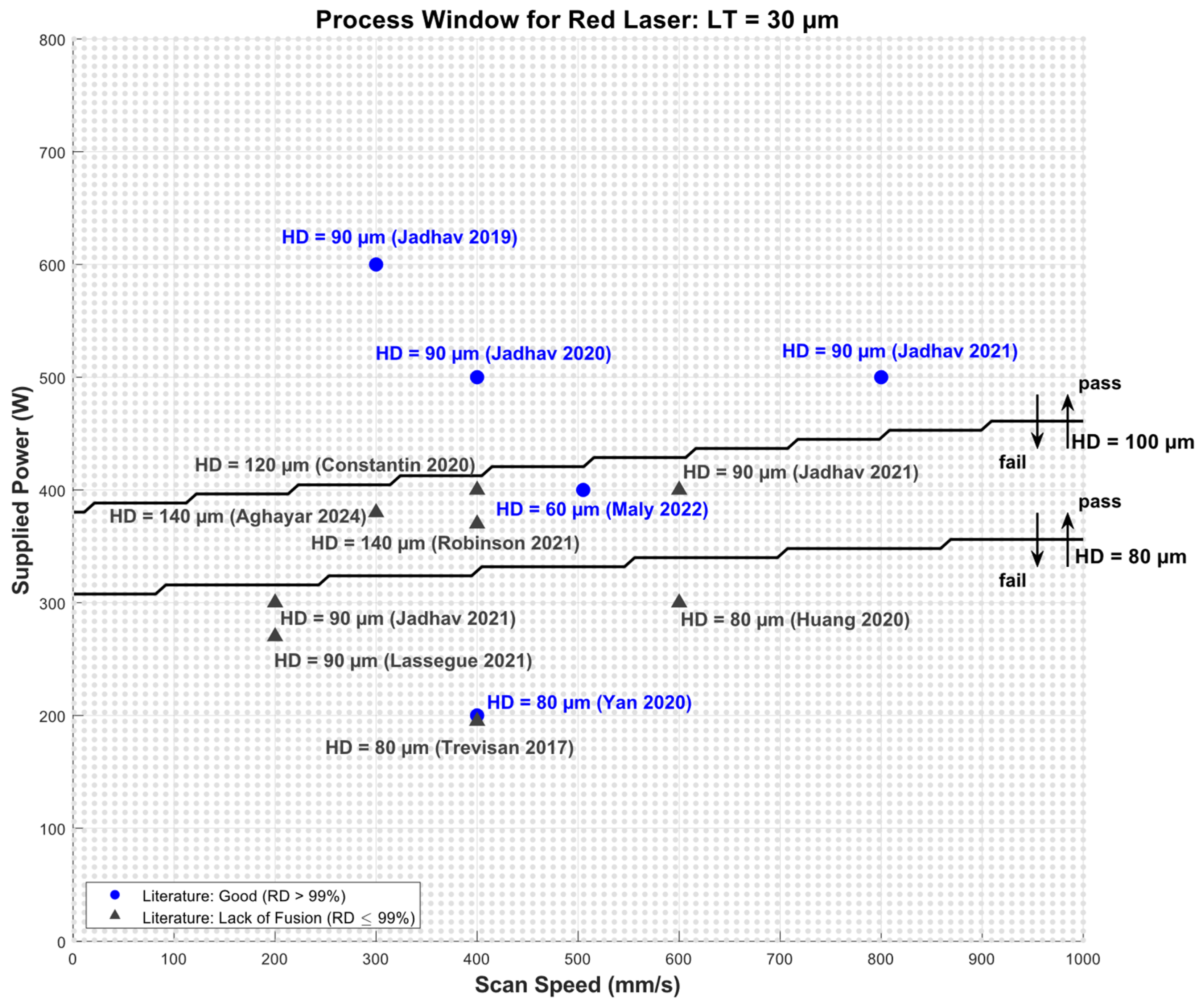
Based on this theory, we can create a process window: for a given layer thickness and hatching distance, we can determine whether any combination of laser power and scanning speed satisfies the LOF conditions. Figure 6 represents the process window for specific hatching distances.
Each black boundary line corresponds to a specific hatching distance and marks the threshold above which the melt pool width becomes sufficient for that HD value. Regions below each black line are predicted to result in lack-of-fusion defects for that specific hatching distance. This layered view of the process window highlights how increasing the hatching distance raises the minimum power and energy input required to achieve a fully fused part. It should be pointed out that changing the layer thickness may also change the minimum power level to prevent a lack of fusion.
To validate the predictive accuracy of this process window, literature-reported parameter sets were overlaid on the model for a 30 µm layer thickness. The results show that good points generally lie well above the HD-specific thresholds, particularly for smaller hatching distances, whereas lack-of-fusion points tend to cluster near or below the boundaries, often at larger HDs where higher power is required to achieve full overlap. One reported data point at 200 W achieved 99% density despite falling inside the predicted failure region, likely reflecting experimental variability or unreported compensating factors such as a smaller effective beam diameter or alternative remelting strategies. It may also reflect the limitations of the Rosenthal approach, which are discussed in the next paragraph. Overall, the close alignment between the literature data and the LOF boundaries confirms that the Rosenthal-based model reliably identifies conditions where incomplete melting occurs.
It is important to note that the LOF criterion only identifies conditions where lack of fusion would occur and does not account for excessive energy input. For instance, sputtering has been observed at powers ≥400 W [88] and 190 W with fine layers [93], while overfusion-related defects were reported at 300–500 W with small hatching distances [98]. However, these observations are scattered across studies and lack consistent power–speed coverage. As such, while the LOF-based process window defines a minimum threshold for complete melting, it does not guarantee optimal processing conditions. In the preceding subsection, it was shown that increasing power beyond ~600 W does not significantly improve relative density and may instead lead to a plateau or even defect formation due to melt pool instability, spatter, and keyhole porosity. These results highlight the need to balance energy input carefully—too little causes a lack of fusion, but too much can degrade part quality. Due to insufficient and fragmented high-energy defect data, we exclude these phenomena from the LOF-based process window and instead address them in the broader discussion of process stability. Additionally, it is worth noting that Rosenthal’s model assumes constant material properties, which is a simplification; in reality, the transition from powder to dense copper alters thermal behavior significantly. The model also treats the laser as a moving point source rather than a Gaussian beam and does not capture melt pool dynamic behavior or beam-to-track overlap effects. These simplifications may contribute to occasional discrepancies between predicted LOF boundaries and individual experimental data points.

2.1.2. Material and Post-Processing Effects

Powder characteristics have been shown to critically affect LPBF of copper across multiple studies. Bonesso et al. [82] demonstrated that phosphorus-doped powders with a 13–28 µm size range achieved 98.3% RD and reduced surface roughness from 12 µm to 2.9 µm, as compared to that from powder with particle size of 15–45 µm. Another study applied surface micro-oxidation to pure copper powder by heating it in air at 160 °C for 1 to 5 min, forming a thin Cu2O layer on the particle surfaces. The 3 min treatment significantly improved relative density and mechanical strength, while longer treatments led to powder agglomeration and reduced flowability [85]. Bonesso et al. [82] also conducted a comparative study across three powders and found that the finest, phosphorus-doped powder achieved the highest RD (98.3%) and surface quality.
Preheating the powder bed improves energy efficiency and melt stability. Maly et al. [86] reported >99% RD at 400 °C preheat, though oxidation and powder agglomeration were concerns. Pre-oxidation of powder prior to processing can also be beneficial. Jadhav et al. [72] and Yang et al. [85] showed that mild oxidation (an oxide layer of less than 1 µm) increased absorptivity, improved melt stability, and significantly enhanced hardness and strength without degrading electrical performance.
Post-build heat treatments further improve mechanical properties. Silbernagel et al. [90] and Yang et al. [85] showed that annealing—particularly at high temperatures near the melting point (e.g., 1000 °C in Silbernagel’s study)—promotes grain growth, reduces porosity, and increases ductility by over 200%. Heat treatment also reduces surface roughness and boosts electrical conductivity through enhanced particle bonding and neck formation [83].

2.1.3. Surface and Functional Properties

Surface roughness in LPBF copper parts is a critical quality metric because it affects post-processing requirements and can degrade electrical and thermal performance. For example, increased surface roughness contributes to higher electrical resistance due to the skin effect, particularly in applications involving high-frequency current flow [83]. It can also necessitate additional finishing steps to meet functional or aesthetic requirements [64]. Surface roughness is also an important parameter in structural application, when the parts fit together and sealing is needed.
Roughness in LPBF copper typically ranges from 3.9 µm to 60 µm [75,83]. It generally decreases with increasing VED and RD but may increase again at excessive energy input due to melt pool instability [78,91]. Qu et al. [60] and others observed smoother surfaces at RD > 99%. Top surfaces are often smoother than side surfaces due to more consistent laser exposure and scanning control, though side roughness can be improved via contour remelting [93].
In addition to VED and RD, several process parameters also influence surface roughness. A reduction in layer thickness was shown to decrease roughness, with 30 µm layers producing smoother surfaces [64]. Powder particle size also plays a role; finer powders significantly improved surface finish, reducing Ra, the average roughness, from 12 µm to 2.9 µm under optimized contour scanning [82].
Electrical conductivity is strongly linked to RD. Near-fully dense parts (>99.5% RD) achieved values up to 96% IACS [81], while parts with RD < 85% showed conductivity as low as 21% IACS [90]. Even small porosities and unmelted regions interrupt electron pathways, as seen in studies by Corona et al. [91], Huang et al. [63], and Abdelhafiz et al. [75]. Conductivity is also influenced by build orientation, with vertically built specimens showing higher resistivity due to interlayer defects [90].
Thermal conductivity improves with RD, though still falls short of cast copper due to residual porosity. Bonesso et al. [82] and Qu et al. [81] reported values up to 383 W/m·K in near-fully dense builds. Lower-density parts (~84%) showed significant reductions in conductivity [91], and Aghayar et al. [80] found that porosity remains the dominant limiting factor, more so than microstructure.
Crack formation remains a key concern in LPBF of copper. Although most mitigation strategies overlap with densification approaches, they warrant specific mention. Excessive energy deposition has been linked to crack initiation [89]. Therefore, excessive energy input must be avoided. Post-build annealing lowers crack susceptibility by relieving residual stresses and shifting fracture behavior from brittle to ductile modes [78], giving the material greater capacity to accommodate strain. Cracks also tend to nucleate at porosity sites, making high relative density essential; optimizing laser power, scan speed, and hatch distance helps stabilize the melt pool, reduce defects, and limit the weak points where cracks can form [62,90].

2.1.4. Mechanical Properties

Mechanical properties of LPBF copper—particularly ultimate tensile strength (UTS), yield strength (YS), ductility, and hardness—are strongly tied to density, microstructure, and the build direction. A comparison between properties achieved with LPBF and traditional copper is shown in Table 2. Lykov et al. [76] reported a UTS of 149 MPa at 88.1% RD, while Aghayar et al. [80] achieved 294 MPa at 98.4% RD. Interestingly, although not pure copper, Yang et al. [85] reported 549 MPa at 95% RD for oxidized copper. Higher strength is associated with finer grains and full melting; porosity and unmelted particles act as stress concentrators [6,63]. Qu et al. [81] demonstrated that in high-precision LPBF of copper, reducing the VED—by increasing scan speed from 600 mm/s to 800 mm/s while keeping laser power constant—produced finer grains (~5.5 µm vs. ~7.5–8.4 µm) and resulted in higher yield strength and improved work-hardening behavior.
Anisotropy in mechanical properties has been consistently observed in IR LPBF of pure copper. Qu et al. [81] reported yield strengths from 195 MPa to 218 MPa and elongation from 20.9% to 33.5%, depending on build orientation and scan strategy, with anisotropy attributed to grain aspect ratio and melt pool geometry. Bonesso et al. [82] found horizontally built pure copper samples reached 254.8 MPa yield strength and 312.7 MPa UTS, while vertically built ones dropped to 237.8 MPa and 259.3 MPa, with elongation decreasing sharply from more than the extensometer limit to 2.36%, due to lack of fusion between layers. Corona et al. [91] observed that horizontal pure copper samples had 129 MPa tensile strength and 5.5% elongation, compared to only 74.7 MPa and 3.3% in vertical builds, with reductions caused by pores and unfused particles aligned with build layers.
Yield strength follows similar trends. Yang et al. [85] reported values up to 452 MPa with surface-oxidized powders; this value reflects modified feedstock and is not directly comparable to pure copper results. In contrast, Bonesso et al. [82] achieved up to 255 MPa using unmodified, pure copper. As expected, heat treatment reduces both UTS and YS [78] but significantly enhances ductility by promoting recrystallization and grain coarsening. Yan et al. [78] observed a 226% increase in ductility following annealing.
Hardness can also be improved through powder optimization and pre-oxidation. Jadhav et al. [72] reported a hardness of 91 HV in oxidized parts, compared to 65 HV in pure copper. While post-processing like annealing slightly reduces hardness, oxidized or fine-powder parts generally maintain superior values [63,82,100].
IR PBF has demonstrated the ability to fabricate thin-walled copper structures with high dimensional accuracy under optimized parameters. In one study, a thin wall structure with a thickness of 156 μm was achieved using a circular scanning strategy that minimized laser energy dispersion outside the intended region [88]. The deviation from the modeled wall thickness (50 µm) was attributed to powder adhesion and surface roughness, but dimensional consistency was maintained along the wall.

2.2. Green Laser with 500–570 nm Wavelengths

Due to the challenges associated with fabricating copper using infrared lasers, laser systems operating at shorter wavelengths around 500 nm—commonly referred to as green lasers—have been introduced for powder bed fusion. These systems were commercialized by companies such as TRUMPF. Research institutes, including Fraunhofer IWS and Fraunhofer ILT, have adopted green laser 3D printers from these manufacturers to improve process efficiency when working with copper [70].
Green LPBF, particularly using a wavelength of 515 nm, offers significantly higher absorptivity in copper compared to IR lasers, as shown in Figure 1. Absorptivity values ranged from 72% to 88% [64,101,102], resulting in improved melt pool stability, reduced porosity, and better geometric accuracy [103]. Studies consistently report high RD—Wagenblast et al. [104] achieved 99.8% RD at VED of 225 J/mm3, and Demir et al. [105] achieved 99.6% at VED as small as 66 J/mm3, indicating efficient densification even at lower energy input. Reported VEDs range from as low as 18 J/mm3 to around 200 J/mm3, with RD improving significantly with optimized scan speed, hatch spacing, and layer thickness [105,106].
LOF defects remain a key issue at low VEDs, while keyholing and overfusion can occur at excessive energy input [105,106,107]. Balancing power and scan speed is critical. Terris et al. [108] showed that a 500 W green laser achieved nearly the same density as a 1 kW IR laser, highlighting green lasers’ superior energy efficiency. High density (>99.5%) was achieved at half the power and lower VEDs (~66–225 J/mm3) compared to the VED of 200–2000 J/mm3 range typically required for IR lasers [105,106,108].
Surface roughness for green laser-printed copper ranges widely, depending on parameters, from 4.66 µm [109] to over 32 µm [64]. Although shorter wavelengths offer higher absorptivity, they can introduce melt pool instability, which may lead to rougher surfaces—especially in parts with higher relative densities—compared to infrared laser systems [109]. Improvements in scanning strategy and remelting techniques can mitigate these effects.
Electrical conductivity in green laser-printed copper consistently reaches 98–100% IACS. Wagenblast et al. [104] reported 100% IACS at 99.8% RD. However, Gruber et al. [101] observed reduced conductivity in thin-walled parts due to surface roughness and pore-induced insulation effects. Conductivity dropped with decreasing wall thickness, despite high overall density.
Thermal conductivity follows similar trends, reaching up to 406 W/m·K at 100 °C [108,110]. Although green laser-built parts initially outperform infrared laser samples, conductivity drops more rapidly at higher temperatures, with infrared parts surpassing green laser samples above 300 °C [108]. This may relate to copper’s electron-dominated heat transport, which decreases at higher temperatures due to intensified electron–phonon scattering. The sharper decline in green laser samples could stem from their finer grains and higher dislocation density, which may increase phonon–defect scattering at elevated temperatures.
Green laser generally produces parts with enhanced mechanical properties. However, the anisotropic effect of additive manufacturing, which results from the layer-by-layer nature of the technique, persists. Vertical specimens (where test orientation is aligned with the build direction) report values between 130 and 133.5 GPa, and horizontal specimens (where test orientation is perpendicular to the build direction) up to 144 GPa [101]. Yield strength, however, shows little anisotropy, with reported values ranging from 135 MPa [101]. to 161 MPa [104]. Tensile strength ranges from 213 to 241 MPa [101,104], aligning with soft-annealed copper and showing less variability than parts made with infrared lasers. A comparison between properties achieved by green LPBF and annealed copper can be seen in Table 3.
Green LPBF also demonstrates strong geometric accuracy and feature resolution. Features below 0.4 mm have been achieved [104], and CAD deviations, measured in lattice structures composed of repeating octet-truss and cuboctahedron unit cells (1.5 mm cell size, ~300 µm strut diameter), remain below 2% in unit-cell dimensions and around 13% in strut diameters [103]. However, minimum printable feature sizes are limited by the scanning vector resolution (~0.5 mm), which arises from the combined effect of the laser beam diameter and the beam compensation settings in the slicing software. Gruber et al. [101] reported that features smaller than 0.5 mm were not converted into scanning vectors due to a 200 µm laser spot and 100 µm beam compensation. However, as noted by the authors, this limitation can potentially be overcome by adjusting the beam compensation (i.e., the offset between the CAD contour and scan path), allowing smaller features to be printed. Wall thickness is influenced by scan track count and build angle, with the smallest walls (~230 µm) formed at shallow angles with multiple scan passes [112].
In summary, green laser LPBF enables high-density, high-conductivity copper printing at lower energy input than infrared lasers. However, challenges with surface roughness, anisotropy, and feature resolution persist. Further optimization of scanning strategies, energy input, and laser focus will be essential for improving part quality in fine-feature applications.

2.3. Electron Beam Powder Bed Fusion

Electron Beam Powder Bed Fusion (EB-PBF) is a PBF technique that utilizes a high-energy electron beam to selectively melt metal powder and build components layer by layer. typically generated by a tungsten filament or a lanthanum hexaboride cathode. Electrons are emitted and then accelerated through a high-voltage potential—commonly 60 kV—and directed using electromagnetic lenses to scan across the powder bed [113].
Metal powder, usually with a particle size around 40–150 µm, is gravity-fed into the chamber and raked into layers across the build plate. Layer thicknesses typically correspond to the size of a few powder particles [114].
Following preheating, a lower-current (5–25 mA), lower-speed (300–1500 mm/s) electron beam scan selectively melts the powder to form the desired geometry layer by layer [115,116,117]. The preheat step is often repeated before each new layer, ensuring stable thermal conditions and improving layer bonding [113].
One of the key advantages of EB-PBF over laser-based systems is its significantly higher energy absorption efficiency. While laser-based systems often suffer from reflection losses, particularly when processing highly reflective metals, EB-PBF achieves approximately 80–90% absorption of the incident beam energy. This efficiency is attributed to the high kinetic energy of electrons and the minimal energy loss due to backscattering under vacuum conditions, allowing more effective melting of the powder bed [118].

EB-PBF Parameters

Typical electron beam systems are defined by two key parameters: beam voltage and beam current, with the beam power calculated as the product of the two (Power = Voltage × Current). In all reviewed studies, the beam voltage was fixed at 60 kV, while the beam power was varied by adjusting the beam current. Several studies have identified optimal power ranges for their respective setup for achieving high density. For example, Ortmann et al. [115] reported that powers between 400 W and 700 W effectively avoided both lack-of-fusion and overheating defects. Similarly, Raab et al. [119]. found that beam powers outside the range of 450–850 W led to porosity caused by insufficient or excessive melting. In contrast to these defined windows, other studies have reported relative densities exceeding 99% across a broader power range of 275–1400 W [77,115,116,119,120,121,122,123,124,125].
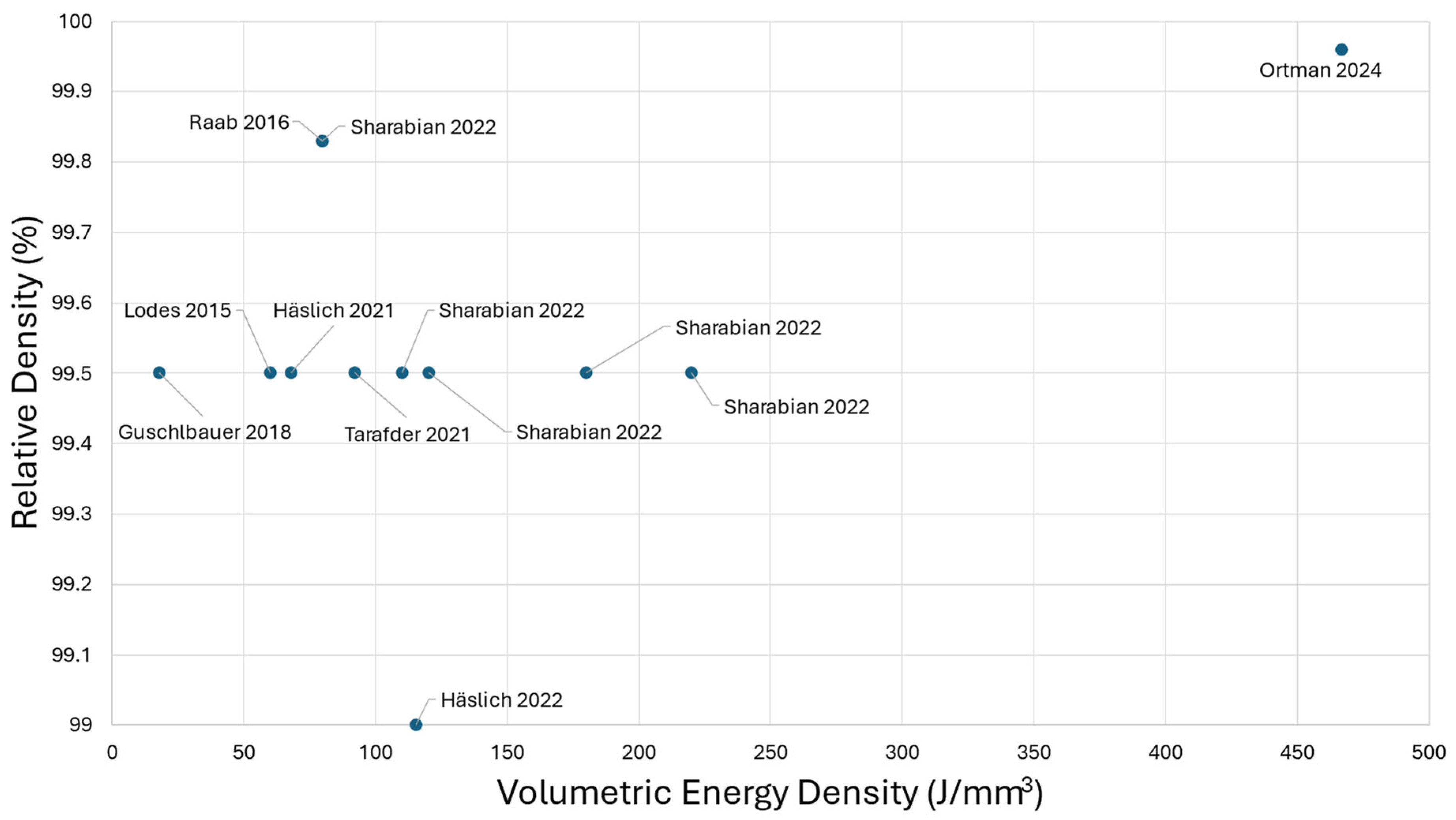
The required VED for E-beam is significantly lower than that of LPBF, with reported values ranging from 55 to 466 J/mm3 [77,115,116,119,120,121,122,123,124,125]. This is expected as laser interactions with the surface obey optical laws, while e-beam interactions follow different physical principles. For e-beam, most studies indicate that a VED in the range of 55–200 J/mm3 is sufficient to achieve >99% RD. This can be seen in Figure 7. The range is comparable to green LPBF and much lower than IR LPBF. The reason for this difference lies in copper’s material properties: its high electrical and thermal conductivity enhances energy absorption under electron beam processing, while its high reflectivity causes energy loss in LPBF. As a result, complete melting and high-density builds can be achieved at significantly lower VED values in EB-PBF.
Similarly to LPBF, the scanning speed does not play a particularly important role and does not impose any significant restrictions. It is used to regulate the volumetric energy density. Unlike LPBF, the scanning speed used in e-beam PBF has a much wider range of 250–5000 mm/s [77,115,116,119,120,121,122,123,124,125]. Although layer thicknesses range from 40 µm to 70 µm, most studies selected 50 µm as a standard value [113,115,116,117,119]. Powder particles generally need to be approximately 45 µm or more in diameter to prevent smoking, a phenomenon in which fine powder particles are ejected from the powder bed due to strong repulsive electrostatic forces induced by the electron beam [114,116]. This restriction in powder diameter limits the use of smaller layer thicknesses. Similarly, the hatch distance ranges from 50 µm to 150 µm, with 100 µm being the most frequently used setting to ensure sufficient overlap and minimize lack-of-fusion porosity [113,115,116,117,119].
In addition to beam parameters, EB-PBF outcomes depend heavily on powder quality, chamber conditions, and thermal control. As mentioned above, to avoid smoking, particles smaller than 45 µm are typically excluded [116]. Furthermore, low-oxygen powders (<0.015 wt%) yield dense, crack-free parts, while higher oxygen levels (>0.0235 wt%) cause intergranular cracking [116].
The process of e-beam melting is performed under high vacuum (10−3–10−4 mbar) with optional helium to reduce charge accumulation [113,119,122]. Vacuum conditions eliminate oxidation and allow high-purity processing without shielding gas [126].
A key advantage of EB-PBF is its preheat stage, where a high-current (approximately 30 mA) electron beam rapidly scans the powder bed to sinter the powder before melting. This pre-sintering step enhances the electrical conductivity of the powder, minimizes the risk of electrostatic repulsion and powder ejection (commonly referred to as “smoking” [113]), and maintains a stable bed temperature throughout the process. Reported preheat temperatures range from 300 °C to over 500 °C, with some cases reaching 1100 °C [113,115,116,119,125,126]. Process monitoring techniques, such as backscattered electron (BSE) imaging and thermal monitoring via thermocouples, are used to ensure consistent conditions [115,117].
Build platforms are typically stainless steel or oxygen-free copper, with standard line offsets of 0.1 mm and support structures ~5 mm high [116,117,119]. Scanning strategies include meander, rotated raster, or contour-hatch patterns, and the beam diameter varies from ~1000 µm (preheat) to ~250 µm (melting) [115].

2.4. Physical and Mechanical Properties of E-Beam Copper Parts

EB-PBF tends to produce copper parts with very high relative density, usually above 99.5%, which is a major advantage over LPBF, where high density is much harder to achieve. That said, one of the trade-offs is surface roughness. EB-PBF parts often exhibit rougher surfaces, with the lowest reported roughness being around 16 µm. For comparison, LPBF parts can reach as low as 3.9 to 5 µm. This roughness comes from the techniques used to avoid the “smoking” effect during EB-PBF, such as using larger powder particles and sintering them before fully melting. Post-processing, such as grain blasting, is often used to remove any remaining loose particles.
In terms of performance, EB-PBF copper has shown electrical conductivity values that reach 101% IACS. Thermal conductivity is also good, with most values coming in slightly above the 385 W/m·K baseline of pure copper. Ultimate strength tends to hover around the same level as pure copper, while yield strength varies more widely—from about 52 to 150 MPa—depending on build orientation and geometry. For example, Guschlbauer et al. [121] reported that 0° specimens (loaded perpendicular to the build plane) achieved 78.1 MPa yield strength and 59.3% elongation, while 45° specimens showed lower ductility (14.3%) and 90° specimens failed prematurely due to vertical cracks. As mentioned previously, parts made using PBF processes are generally anisotropic, with properties depending on the orientation relative to the build direction [127,128,129]. The elastic modulus depends on the direction of measurement due to grain structure but typically centers around 110 GPa, matching pure copper. In a study conducted by Guschlbauer et al. [126], the Young’s modulus was measured as 121.1 ± 4.7 GPa in the build direction (0°, [001]), 145.5 ± 1.6 GPa in-plane (90°, [110]), and 133.5 ± 2.3 GPa at 45° ([111]), indicating only mild anisotropy. These values are comparable to or slightly above the isotropic value of 121 GPa for polycrystalline copper. Hardness, on the other hand, is consistently higher—even reaching above 100 HV [77] —due to the rapid cooling rates during EB-PBF, which create a finer microstructure. The comparison between the performance of EB-PBF of copper and standard annealed copper can be seen in Table 4.

2.5. Benefits of EB-PBF/Application to Copper AM

EB-PBF offers several advantages that make it particularly well-suited for copper. One of its primary strengths is the high-power output of the electron beam, which allows for more complete melting of the powder and supports higher scanning speeds. These factors result in significantly faster build times compared to other AM processes [59].
In addition to its power, EB-PBF features rapid and precise beam deflection. Controlled by electromagnetic coils, the beam can shift almost instantaneously between locations, enabling the fabrication of complex geometries that mighi)t be challenging or time-consuming with other techniques. This high-speed deflection capability complements the system’s overall efficiency [77].
EB-PBF uses electrons rather than photons, eliminating the longstanding issue of copper’s high optical reflectivity—a major limitation in laser-based systems like IR LPBF. Combined with the system’s inherently higher energy delivery, EB-PBF is particularly well-suited for processing highly conductive and reflective materials such as copper [59].
Moreover, unlike many metals that suffer from electrical charging effects during EB-PBF processing, copper’s high electrical conductivity enables it to perform reliably under these conditions. This not only ensures process stability but also takes full advantage of the EB-PBF system’s design benefits [130].

2.6. Limitations/Issues to Resolve

EB-PBF presents several unique challenges, the most well-known being the phenomenon known as smoking. This occurs when the powder suddenly erupts upward in a plume, filling the build chamber with a fine cloud that halts the process entirely and necessitates complete cleaning before printing can resume. Smoking is extensively studied in the context of EB-PBF, and mitigation strategies such as defocused scanning to pre-sinter the powder and powder pre-treatment via ball milling or heat treatment have shown some effectiveness in reducing its occurrence [114]. The prevailing hypothesis attributes the phenomenon to excessive static charge accumulation: when electrostatic repulsion between powder particles exceeds the gravitational force on each particle, the powder erupts upward. However, the underlying mechanisms are not completely understood, and current mitigation techniques only reduce the frequency of its occurrence rather than eliminate the issue.
In some studies, hydrogen heat treatment is used on raw powder prior to building to remove oxygen. This process can lead to the formation of internal water vapor pockets. Given the high energy of the electron beam, these vapor pockets may rupture violently during processing, resulting in spatter defects on the part surface. Ledford et al. [130] developed complex methods to safely release the internal vapor and prevent damage to the printed parts [130]. However, these methods required specialized and costly custom equipment, limiting their practicality for widespread use.
At the other extreme, EB-PBF’s exceptionally high scanning speeds can result in low VED, which promotes melt pool instability and leads to defects such as balling [59].

3. Discussion

Despite significant progress in LPBF and EB-PBF of copper, including broader reviews that examine general trends across various metallic systems [131], several important research gaps remain unaddressed. Most studies have primarily focused on achieving high RD and electrical conductivity, yet they rarely examine geometric accuracy or feature resolution, particularly in the context of thin-walled or micro-scale structures. Although some green and infrared laser systems have demonstrated the ability to fabricate features as small as 0.1 mm [82,92], systematic investigations into thin-wall fabrication, which is critical for applications such as microchannels and antennas, are largely absent across both red and green laser-based studies.
Another notable gap concerns the optimization of beam diameter in green laser systems. While green lasers offer superior absorptivity and process stability, most studies utilize relatively large beam diameters (200 µm), which limits the feature size.
Furthermore, strategies to control mechanical anisotropy are underdeveloped, despite documented anisotropic strength and ductility in LPBF copper samples, particularly due to grain boundary distributions [76,84]. Similarly, although porosity is typically considered a defect, its deliberate use to tailor thermal, electrical, and mechanical properties—or enhance biocompatibility—remains largely unexplored in copper additive manufacturing.
One of the main challenges in PBF of copper is its low absorption coefficient at infrared wavelengths. While the use of green lasers has significantly mitigated this issue, alternative approaches to enhance copper powder absorptivity remain relatively underexplored. Powder functionalization, for instance, is still not widely adopted. Most studies focus on optimizing laser parameters, while fewer investigate surface modifications or coatings designed to improve infrared absorptivity and, in turn, influence the physical properties of the printed part [132]. These strategies could be especially beneficial for improving red laser printability, where copper’s high reflectivity remains a critical limitation. However, surface modification typically involves coating the powder with an oxide [72] or a foreign element [133,134], which can alter the chemical composition and final properties of the part. For example, zinc-coated copper powder [133] has been shown to improve laser absorptivity significantly. Although much of the zinc evaporates during the PBF process, residual traces can still be detected on the melt track surfaces. Further research is needed to develop coating materials that fully vaporize during processing, thereby enhancing absorptivity without compromising the chemical purity of the printed copper component.
Based on current literature trends, red lasers—with appropriately reduced spot sizes—may be better suited for applications requiring fine features and geometric precision, provided that absorptivity challenges are mitigated through powder modification or adopting higher laser powers. Green lasers, on the other hand, offer the most robust and energy-efficient process window for printing bulk copper parts with high electrical conductivity. EB-PBF systems provide unique advantages such as high build quality, oxygen control, and in situ monitoring.
Future research should aim to systematically benchmark the minimum wall thickness and resolution capabilities achievable across both LPBF and EB-PBF systems, particularly in the context of complex geometries and fine-feature fabrication. Additionally, the impact of sub-100 µm beam diameters in green laser platforms warrants investigation, as smaller spot sizes may enable improved precision for microscale applications. An additional opportunity is the exploration of multi-laser PBF, which can improve the build rate [135]. No such studies have yet been reported for copper, but future work could evaluate whether these parallelized energy sources can reduce build times while maintaining part quality. Another promising direction involves the development and testing of functionalized copper powders, such as those coated with carbon-based or oxide materials, to enhance laser absorptivity—particularly for infrared systems. Finally, there is a need to integrate known defect thresholds, including lack of fusion, sputtering, and over fusion, into formalized process window models to improve predictability and control in copper additive manufacturing.
Parameter recommendations were developed based on both literature trends and internal simulations. For red laser LPBF, we recommend a 30 µm layer thickness, balancing density with recoating reliability and powder cost. Hatch distances of 50–100 µm are commonly associated with dense builds, and laser powers exceeding 400 W are supported by Rosenthal-based thermal modeling. While scan speed varies, it should be selected to maintain a VED of 400–500 J/mm3, which consistently yields >98% RD in published work.
For green laser LPBF, the same 30 µm layer thickness is suggested. Due to improved absorptivity, a wider hatch spacing of 100–150 µm is typically sufficient. Although successful prints have been reported across a broad power range (50–1000 W), we recommend using >200 W based on internal simulations indicating more stable melting at this threshold. Owing to broader variability in parameter combinations, no specific VED range is proposed, but further data could help identify a reliable target window.
In EB-PBF, typical settings include 60 kV beam voltage, 15–20 mA current (~1200 W), and 3 m/s scan speed, which together produce dense parts while maintaining melt pool control. A layer thickness of 50 µm is generally used, matching the average powder size (~45 µm) to help suppress the smoking effect. A hatch spacing of 100 µm is standard across most studies and appears to reliably support full density.

4. Conclusions

Although the industrial application of PBF for copper remains limited, it offers several advantages over conventional powder sintering, including the ability to achieve higher densification and to fabricate geometries that are difficult or impossible to produce using traditional die-compaction methods [136,137,138,139].
Green lasers and EB-PBF offer significant advantages over IR lasers for the powder bed fusion of copper, consistently achieving higher relative densities (97% or higher for green laser, 99.5% or higher for electron beam) and superior electrical conductivity (often near 100% IACS for green laser, and sometimes even above 100% for electron beam). Green lasers operate more energy-efficiently, achieving high densities at lower volumetric energy densities compared to NIR lasers, while electron beam operates much more rapidly with fewer impurities than lasers and also with lower VED. Green laser and electron beam-fabricated copper parts also exhibit higher ultimate and yield strengths, with mechanical properties that align closely with those of conventionally processed copper, making them a promising technology for high-performance applications.
A key question is whether green laser PBF will prove to be a future-proof method: while it provides significant energy efficiency compared to infrared lasers, current systems rely on larger beam diameters, leading to lower resolution and higher surface roughness than red lasers. Moreover, green lasers do not improve the absorptivity significantly for common PBF alloys such as Ti-6Al-4V and steel [140,141]. Unless optical improvements allow smaller beam sizes and the cost of adopting separate green laser systems becomes economically justified by industrial demand for copper PBF, the widespread switch to green lasers may not be necessary.
Despite these challenges, further process optimizations, such as enhanced remelting strategies and improved powder management, could mitigate surface quality issues, and ongoing research will determine whether green laser PBF can evolve into a broadly adopted, future-proof solution. Overall, green lasers and electron beams offer more consistent, higher-quality, and more efficient routes for producing copper parts, although continued advances are needed to expand their adoption across industry.

Supplementary Materials

The following supporting information can be downloaded at: https://www.mdpi.com/article/10.3390/met15101114/s1, Table S1: List of papers used for data analysis and summary of key processing parameters for LPBF of copper; Table S2: List of papers used for data analysis and summary of key processing parameters for EB-PBF of copper.

Author Contributions

Conceptualization, V.H. and L.L.; methodology, V.H. and L.L.; investigation, V.H.; data curation, V.H.; formal analysis, V.H., L.L., S.G., A.B.M. and C.C.; resources, S.G. and E.L.; visualization, V.H., L.L., S.G., A.B.M. and C.C.; writing—original draft, V.H.; writing—review and editing, V.H., L.L., A.B.M., C.C., S.G., E.L., J.R. and D.E.; validation, A.B.M., C.C., S.G., J.R. and D.E.; supervision, L.L., E.L. and J.R.; project administration, L.L.; funding acquisition, L.L. All authors have read and agreed to the published version of the manuscript.

Funding

This work is supported through National Science Foundation National Research Traineeship Program grant number 2152254.

Acknowledgments

The authors acknowledge support from the National Science Foundation National Research Traineeship Program (Grant No. 2152254) and the assistance of Jonathan Schaefer in collecting literature.

Conflicts of Interest

The authors declare no conflicts of interest.

References

  1. Elshkaki, A.; Graedel, T.E.; Ciacci, L.; Reck, B.K. Copper demand, supply, and associated energy use to 2050. Glob. Environ. Change 2016, 39, 305–315. [Google Scholar] [CrossRef]
  2. Economic Impact-$160B Role in the, U.S. Economy. Available online: https://copper.org/economy/ (accessed on 7 July 2024).
  3. Helmenstine, A.H. Table of Electrical Resistivity and Conductivity. Available online: https://www.thoughtco.com/table-of-electrical-resistivity-conductivity-608499 (accessed on 7 July 2024).
  4. Askeland, D.R. The Science and Engineering of Materials; Springer: Boston, MA, USA, 1996. [Google Scholar] [CrossRef]
  5. Zhou, H.; Chang, A.; Fan, J.; Cao, J.; An, B.; Xia, J.; Yao, J.; Cui, X.; Zhang, Y. Copper Wire Bonding: A Review. Micromachines 2023, 14, 1612. [Google Scholar] [CrossRef]
  6. Robinson, J.; Arjunan, A.; Baroutaji, A.; Stanford, M. Mechanical and thermal performance of additively manufactured copper, silver and copper–silver alloys. Proc. Inst. Mech. Eng. Part L J. Mater. Des. Appl. 2021, 239, 1877–1891. [Google Scholar] [CrossRef]
  7. Khan, Z.A. A Novel Transmission Line Structure for High-Speed High-Density Copper Interconnects. IEEE Trans. Compon. Packag. Manufact. Technol. 2016, 6, 1077–1086. [Google Scholar] [CrossRef]
  8. Thieman, M.; Kamm, R.; Jorstad, J. Copper motor rotors: Energy saving efficiency, now also economic feasibility. In 2007 Electrical Insulation Conference and Electrical Manufacturing Expo; IEEE: Nashville, TN, USA, 2007; pp. 328–333. [Google Scholar] [CrossRef]
  9. Stark, C.; Cowie, J.G.; Peters, D.T.; Brush, E.F. Copper in the Rotor for Lighter, Longer Lasting Motors. Available online: https://www.researchgate.net/profile/John-Cowie/publication/265097366_Copper_in_the_Rotor_for_Lighter_Longer_Lasting_Motors/links/54411c5e0cf2a76a3cc7ca04/Copper-in-the-Rotor-for-Lighter-Longer-Lasting-Motors.pdf (accessed on 3 November 2024).
  10. Liu, Y.; Yin, L.; Bliznakov, S.; Kondos, P.; Borgesen, P.; Henderson, D.W.; Parks, C.; Wang, J.; Cotts, E.J.; Dimitrov, N. Improving Copper Electrodeposition in the Microelectronics Industry. IEEE Trans. Comp. Packag. Technol. 2010, 33, 127–137. [Google Scholar] [CrossRef]
  11. Siau, S.; Vervaet, A.; Van Vaeck, L.; Schacht, E.; Demeter, U.; Van Calster, A. Adhesion Strength of the Epoxy Polymer/Copper Interface for Use in Microelectronics. J. Electrochem. Soc. 2005, 152, C442. [Google Scholar] [CrossRef]
  12. Zhao, M.; Kariuki, S.; Dewald, H.D.; Lemke, F.R.; Staniewicz, R.J.; Plichta, E.J.; Marsh, R.A. Electrochemical Stability of Copper in Lithium-Ion Battery Electrolytes. J. Electrochem. Soc. 2000, 147, 2874. [Google Scholar] [CrossRef]
  13. Zeng, X.; He, P.; Hu, M.; Zhao, W.; Chen, H.; Liu, L.; Sun, J.; Yang, J. Copper inks for printed electronics: A review. Nanoscale 2022, 14, 16003–16032. [Google Scholar] [CrossRef]
  14. Tomotoshi, D.; Kawasaki, H. Surface and Interface Designs in Copper-Based Conductive Inks for Printed/Flexible Electronics. Nanomaterials 2020, 10, 1689. [Google Scholar] [CrossRef]
  15. Jason, N.N.; Shen, W.; Cheng, W. Copper Nanowires as Conductive Ink for Low-Cost Draw-On Electronics. ACS Appl. Mater. Interfaces 2015, 7, 16760–16766. [Google Scholar] [CrossRef]
  16. Jia, S.Q.; Yang, F. High thermal conductive copper/diamond composites: State of the art. J. Mater. Sci. 2021, 56, 2241–2274. [Google Scholar] [CrossRef]
  17. Miner, D.K. New Technology for Copper and Brass Radiators. In Proceedings of the SAE International Congress and Exposition, McLean, VA, USA, 1 February 1987. [Google Scholar] [CrossRef]
  18. Sharma, M.; Narayan Vishwakarma, P.; Sharma, A.; Shubham, P. Performance Investigation of Copper and Aluminium Radiators for Lower HP Tractor Engines. J. Phys. Conf. Ser. 2022, 2178, 012011. [Google Scholar] [CrossRef]
  19. Dhaou, H.; Ben Khedher, N.; Mellouli, S.; Souahlia, A.; Askri, F.; Jemni, A.; Ben Nasrallah, S. Improvement of thermal performance of spiral heat exchanger on hydrogen storage by adding copper fins. Int. J. Therm. Sci. 2011, 50, 2536–2542. [Google Scholar] [CrossRef]
  20. Pakalka, S.; Valančius, K.; Streckienė, G. Experimental comparison of the operation of PCM-based copper heat exchangers with different configurations. Appl. Therm. Eng. 2020, 172, 115138. [Google Scholar] [CrossRef]
  21. Barros, L.Y.; Poletto, J.C.; Neis, P.D.; Ferreira, N.F.; Pereira, C.H.S. Influence of copper on automotive brake performance. Wear 2019, 426, 741–749. [Google Scholar] [CrossRef]
  22. Österle, W.; Prietzel, C.; Kloß, H.; Dmitriev, A.I. On the role of copper in brake friction materials. Tribol. Int. 2010, 43, 2317–2326. [Google Scholar] [CrossRef]
  23. Arendsen, L.P.; Thakar, R.; Sultan, A.H. The Use of Copper as an Antimicrobial Agent in Health Care, Including Obstetrics and Gynecology. Clin. Microbiol. Rev. 2019, 32, e00125-18. [Google Scholar] [CrossRef]
  24. Vincent, M.; Hartemann, P.; Engels-Deutsch, M. Antimicrobial applications of copper. Int. J. Hyg. Environ. Health 2016, 219, 585–591. [Google Scholar] [CrossRef]
  25. Casey, A.L.; Adams, D.; Karpanen, T.J.; Lambert, P.A.; Cookson, B.D.; Nightingale, P.; Miruszenko, L.; Shillam, R.; Christian, P.; Elliott, T.S.J. Role of copper in reducing hospital environment contamination. J. Hosp. Infect. 2010, 74, 72–77. [Google Scholar] [CrossRef]
  26. Marais, F.; Mehtar, S.; Chalkley, L. Antimicrobial efficacy of copper touch surfaces in reducing environmental bioburden in a South African community healthcare facility. J. Hosp. Infect. 2010, 74, 80–82. [Google Scholar] [CrossRef]
  27. Ibrahim, Z.; Petrusan, A.J.; Hooke, P.; Hinsa-Leasure, S.M. Reduction of bacterial burden by copper alloys on high-touch athletic center surfaces. Am. J. Infect. Control 2018, 46, 197–201. [Google Scholar] [CrossRef]
  28. Cervantes, H.I.; Álvarez, J.A.; Muñoz, J.M.; Arreguín, V.; Mosqueda, J.L.; Macías, A.E. Antimicrobial activity of copper against organisms in aqueous solution: A case for copper-based water pipelines in hospitals? Am. J. Infect. Control 2013, 41, e115–e118. [Google Scholar] [CrossRef]
  29. Sudha, V.B.P.; Singh, K.O.; Prasad, S.R.; Venkatasubramanian, P. Killing of enteric bacteria in drinking water by a copper device for use in the home: Laboratory evidence. Trans. R. Soc. Trop. Med. Hyg. 2009, 103, 819–822. [Google Scholar] [CrossRef] [PubMed]
  30. Bisht, N.; Dwivedi, N.; Kumar, P.; Venkatesh, M.; Yadav, A.K.; Mishra, D.; Solanki, P.; Verma, N.K.; Lakshminarayanan, R.; Ramakrishna, S.; et al. Recent advances in copper and copper-derived materials for antimicrobial resistance and infection control. Curr. Opin. Biomed. Eng. 2022, 24, 100408. [Google Scholar] [CrossRef] [PubMed]
  31. Fateh, A.; Aliofkhazraei, M.; Rezvanian, A.R. Review of corrosive environments for copper and its corrosion inhibitors. Arab. J. Chem. 2020, 13, 481–544. [Google Scholar] [CrossRef]
  32. Vargas, I.T.; Alsina, M.A.; Pavissich, J.P.; Jeria, G.A.; Pastén, P.A.; Walczak, M.; Pizarro, G.E. Multi-technique approach to assess the effects of microbial biofilms involved in copper plumbing corrosion. Bioelectrochemistry 2014, 97, 15–22. [Google Scholar] [CrossRef]
  33. Schock, M.R.; Lytle, D.A. Control of Copper Corrosion of Household Plumbing Materials; United States Environmental Protection Agency: Cincinnati, OH, USA, 1995. [Google Scholar]
  34. Keevil, C.W. The physico-chemistry of biofilm-mediated pitting corrosion of copper pipe supplying potable water. Water Sci. Technol. 2004, 49, 91–98. [Google Scholar] [CrossRef]
  35. Lin, S.; Li, D.; Zhou, Q.; Chu, M.; Sun, Y.; Liu, M.; Zheng, K.; Qiao, S.; Zhao, L.; Zhao, L.; et al. Study on corrosion perforation behavior of copper nickel alloy pipe during service in marine environment. Eng. Fail. Anal. 2023, 153, 107628. [Google Scholar] [CrossRef]
  36. Gilbert, P.T. Corrosion Resisting Properties of 90/10 Copper–Nickel–Iron Alloy with Particular Reference to Offshore Oil and Gas Applications. Br. Corros. J. 1979, 14, 20–25. [Google Scholar] [CrossRef]
  37. Wallinder, I.O.; Verbiest, P.; He, W.; Leygraf, C. Effects of exposure direction and inclination on the runff rates of zinc and copper roofs. Corros. Sci. 2000, 42, 1471–1487. [Google Scholar] [CrossRef]
  38. Pennington, S.L.; Webster-Brown, J.G. Stormwater runoff quality from copper roofing, Auckland, New Zealand. N. Z. J. Mar. Freshw. Res. 2008, 42, 99–108. [Google Scholar] [CrossRef]
  39. Özkavak, H.V.; Gode, C. Machinability of pure copper before and after processing by severe plastic deformation method. Proc. Inst. Mech. Eng. Part B J. Eng. Manuf. 2022, 236, 1526–1534. [Google Scholar] [CrossRef]
  40. Yang, H.M.; Guo, Z.; Xiong, S.M. Microstructure and mechanical properties of high-pressure die cast pure copper. J. Mater. Process. Technol. 2020, 275, 116377. [Google Scholar] [CrossRef]
  41. Smith, P.H. Cutting Casting Costs. Sci. Am. 1935, 152, 254–257. [Google Scholar] [CrossRef]
  42. Idodo, P.; Rayan, S. Reducing Casting Defects in Pure Copper Castings. Bachelor’s Thesis, Jönköping School of Engineering, Jönköping, Sweden, 2022. [Google Scholar]
  43. Malec, W.; Kulasa, J.; Brudny, A.; Hury, A.; Adamczyk, B.; Rzepecki, R.; Sekula, R.; Kmita, G.; Rybak, A. Comparative Studies of the Properties of Copper Components: Conventional vs. Additive Manufacturing Technologies. Metals 2024, 14, 975. [Google Scholar] [CrossRef]
  44. Jiang, Q.; Zhang, P.; Yu, Z.; Shi, H.; Wu, D.; Yan, H.; Ye, X.; Lu, Q.; Tian, Y. A Review on Additive Manufacturing of Pure Copper. Coatings 2021, 11, 740. [Google Scholar] [CrossRef]
  45. Wong, K.V.; Hernandez, A. A Review of Additive Manufacturing. ISRN Mech. Eng. 2012, 2012, 208760. [Google Scholar] [CrossRef]
  46. Derekar, K.S. A review of wire arc additive manufacturing and advances in wire arc additive manufacturing of aluminium. Mater. Sci. Technol. 2018, 34, 895–916. [Google Scholar] [CrossRef]
  47. Casalino, G.; Karamimoghadam, M.; Contuzzi, N. Metal Wire Additive Manufacturing: A Comparison between Arc Laser and Laser/Arc Heat Sources. Inventions 2023, 8, 52. [Google Scholar] [CrossRef]
  48. Osipovich, K.; Kalashnikov, K.; Chumaevskii, A.; Gurianov, D.; Kalashnikova, T.; Vorontsov, A.; Zykova, A.; Utyaganova, V.; Panfilov, A.; Nikolaeva, A.; et al. Wire-Feed Electron Beam Additive Manufacturing: A Review. Metals 2023, 13, 279. [Google Scholar] [CrossRef]
  49. Shaikh, M.O.; Chen, C.-C.; Chiang, H.-C.; Chen, J.-R.; Chou, Y.-C.; Kuo, T.-Y.; Ameyama, K.; Chuang, C.-H. Additive manufacturing using fine wire-based laser metal deposition. RPJ 2019, 26, 473–483. [Google Scholar] [CrossRef]
  50. Taheri, H. Powder-based additive manufacturing–a review of types of defects, generation mechanisms, detection, property evaluation and metrology. Int. J. Addit. Subtractive Mater. Manuf. 2017, 1, 172–209. [Google Scholar] [CrossRef]
  51. Shanthar, R.; Chen, K.; Abeykoon, C. Powder-Based Additive Manufacturing: A Critical Review of Materials, Methods, Opportunities, and Challenges. Adv. Eng. Mater. 2023, 25, 2300375. [Google Scholar] [CrossRef]
  52. Ziaee, M.; Crane, N.B. Binder jetting: A review of process, materials, and methods. Addit. Manuf. 2019, 28, 781–801. [Google Scholar] [CrossRef]
  53. Svetlizky, D.; Das, M.; Zheng, B.; Vyatskikh, A.L.; Bose, S.; Bandyopadhyay, A.; Schoenung, J.M.; Lavernia, E.J.; Eliaz, N. Directed energy deposition (DED) additive manufacturing: Physical characteristics, defects, challenges and applications. Mater. Today 2021, 49, 271–295. [Google Scholar] [CrossRef]
  54. Medová, D.; Knaislová, A.; Strakosova, A.; Molnárová, O.; Čapek, J.; Voňavková, I.; Vojtěch, D. Comparison of direct energy deposition and powder bed fusion technology in the preparation of Ti–6Al–4V alloy. J. Mater. Res. Technol. 2025, 35, 3825–3840. [Google Scholar] [CrossRef]
  55. Babuska, T.F.; Krick, B.A.; Susan, D.F.; Kustas, A.B. Comparison of powder bed fusion and directed energy deposition for tailoring mechanical properties of traditionally brittle alloys. Manuf. Lett. 2021, 28, 30–34. [Google Scholar] [CrossRef]
  56. Demeneghi, G.; Gradl, P.; Mayeur, J.R.; Hazeli, K. GRCop-42: Comparison between laser powder Bed fusion and direct energy deposition. Addit. Manuf. Lett. 2024, 10, 100224. [Google Scholar] [CrossRef]
  57. DIN EN ISO/ASTM 52900:2022-03; Additive Fertigung_- Grundlagen_- Terminologie (ISO/ASTM 52900:2021); Deutsche Fassung EN_ISO/ASTM 52900. DIN Media GmbH: Berlin, Germany, 2021. [CrossRef]
  58. Tran, T.Q.; Chinnappan, A.; Lee, J.K.Y.; Loc, N.H.; Tran, L.T.; Wang, G.; Kumar, V.V.; Jayathilaka, W.A.D.M.; Ji, D.; Doddamani, M.; et al. 3D Printing of Highly Pure Copper. Metals 2019, 9, 756. [Google Scholar] [CrossRef]
  59. Ladani, L.; Sadeghilaridjani, M. Review of Powder Bed Fusion Additive Manufacturing for Metals. Metals 2021, 11, 1391. [Google Scholar] [CrossRef]
  60. Tang, M.; Pistorius, P.C.; Beuth, J.L. Prediction of lack-of-fusion porosity for powder bed fusion. Addit. Manuf. 2017, 14, 39–48. [Google Scholar] [CrossRef]
  61. Wang, L.; Zhang, Y.; Chia, H.Y.; Yan, W. Mechanism of keyhole pore formation in metal additive manufacturing. npj Comput. Mater. 2022, 8, 22. [Google Scholar] [CrossRef]
  62. Qu, S.; Ding, J.; Fu, J.; Fu, M.; Zhang, B.; Song, X. High-precision laser powder bed fusion processing of pure copper. Addit. Manuf. 2021, 48, 102417. [Google Scholar] [CrossRef]
  63. Huang, J.; Yan, X.; Chang, C.; Xie, Y.; Ma, W.; Huang, R.; Zhao, R.; Li, S.; Liu, M.; Liao, H. Pure copper components fabricated by cold spray (CS) and selective laser melting (SLM) technology. Surf. Coat. Technol. 2020, 395, 125936. [Google Scholar] [CrossRef]
  64. Domine, A.; Verdy, C.; Penaud, C.; Vitu, L.; Fenineche, N.; Dembinski, L. Selective laser melting (SLM) of pure copper using 515-nm green laser: From single track analysis to mechanical and electrical characterization. Int. J. Adv. Manuf. Technol. 2023, 1–12. [Google Scholar] [CrossRef]
  65. Advantages and Development Prospects of 405nm 445nm 450nm and Other Blue Lasers. Available online: https://www.s-laser.com/info/advantages-development-prospects-blue-laser-77888493.html (accessed on 7 July 2025).
  66. Tepylo, N.; Huang, X.; Patnaik, P.C. Laser-Based Additive Manufacturing Technologies for Aerospace Applications. Adv. Eng. Mater. 2019, 21, 1900617. [Google Scholar] [CrossRef]
  67. Kim, Y.-Y.; Joo, J.-Y.; Kim, J.-M.; Lee, S.-K. Compact Measurement of the Optical Power in High-Power LED Using a Light-Absorbent Thermal Sensor. Sensors 2021, 21, 4690. [Google Scholar] [CrossRef]
  68. Ikeshoji, T.-T.; Nakamura, K.; Yonehara, M.; Imai, K.; Kyogoku, H. Selective Laser Melting of Pure Copper. JOM 2018, 70, 396–400. [Google Scholar] [CrossRef]
  69. Jadhav, S.D.; Dadbakhsh, S.; Goossens, L.; Kruth, J.-P.; Van Humbeeck, J.; Vanmeensel, K. Influence of selective laser melting process parameters on texture evolution in pure copper. J. Mater. Process. Technol. 2019, 270, 47–58. [Google Scholar] [CrossRef]
  70. TRUMPF Introduces Precious Metal and Copper 3D Printing Powered by Green Laser-3D Printing Industry. Available online: https://3dprintingindustry.com/news/trumpf-introduces-precious-metal-and-copper-3d-printing-powered-by-green-laser-143689/ (accessed on 10 September 2024).
  71. Hori, E.; Sato, Y.; Shibata, T.; Tojo, K.; Tsukamoto, M. Development of SLM process using 200 W blue diode laser for pure copper additive manufacturing of high density structure. J. Laser Appl. 2021, 33, 012008. [Google Scholar] [CrossRef]
  72. Jadhav, S.D.; Vleugels, J.; Kruth, J.; Van Humbeeck, J.; Vanmeensel, K. Mechanical and electrical properties of selective laser-melted parts produced from surface-oxidized copper powder. Mat. Des. Process. Comms. 2020, 2, e94. [Google Scholar] [CrossRef]
  73. Colopi, M.; Caprio, L.; Demir, A.G.; Previtali, B. Selective laser melting of pure Cu with a 1 kW single mode fiber laser. Procedia CIRP 2018, 74, 59–63. [Google Scholar] [CrossRef]
  74. Colopi, M.; Demir, A.G.; Caprio, L.; Previtali, B. Limits and solutions in processing pure Cu via selective laser melting using a high-power single-mode fiber laser. Int. J. Adv. Manuf. Technol. 2019, 104, 2473–2486. [Google Scholar] [CrossRef]
  75. Abdelhafiz, M.; Al-Rubaie, K.S.; Emadi, A.; Elbestawi, M.A. Process–Structure–Property Relationships of Copper Parts Manufactured by Laser Powder Bed Fusion. Materials 2021, 14, 2945. [Google Scholar] [CrossRef] [PubMed]
  76. Lykov, P.; Baytimerov, R.; Vaulin, S.; Safonov, E.; Zherebtsov, D. Selective Laser Melting of Copper by 200 W CO2 Laser. In Proceedings of the SAE 2016 World Congress and Exhibition, Chelyabinsk, Russia, 5 April 2016. [Google Scholar] [CrossRef]
  77. Sharabian, E.; Leary, M.; Fraser, D.; Gulizia, S. Electron beam powder bed fusion of copper components: A review of mechanical properties and research opportunities. Int. J. Adv. Manuf. Technol. 2022, 122, 513–532. [Google Scholar] [CrossRef]
  78. Yan, X.; Chang, C.; Dong, D.; Gao, S.; Ma, W.; Liu, M.; Liao, H.; Yin, S. Microstructure and mechanical properties of pure copper manufactured by selective laser melting. Mater. Sci. Eng. A 2020, 789, 139615. [Google Scholar] [CrossRef]
  79. Jadhav, S.D.; Goossens, L.R.; Kinds, Y.; Hooreweder, B.V.; Vanmeensel, K. Laser-based powder bed fusion additive manufacturing of pure copper. Addit. Manuf. 2021, 42, 101990. [Google Scholar] [CrossRef]
  80. Aghayar, Y.; Moazzen, P.; Behboodi, B.; Shahriari, A.; Shakerin, S.; Lloyd, A.; Mohammadi, M. Laser powder bed fusion of pure copper electrodes. Mater. Des. 2024, 239, 112742. [Google Scholar] [CrossRef]
  81. Qu, S.; Ding, J.; Fu, J.; Fu, M.; Song, X. Anisotropic material properties of pure copper with fine-grained microstructure fabricated by laser powder bed fusion process. Addit. Manuf. 2022, 59, 103082. [Google Scholar] [CrossRef]
  82. Bonesso, M.; Rebesan, P.; Gennari, C.; Mancin, S.; Dima, R.; Pepato, A.; Calliari, I. Effect of Particle Size Distribution on Laser Powder Bed Fusion Manufacturability of Copper. BHM Berg-Und Huettenmaenn Monatsh. 2021, 166, 256–262. [Google Scholar] [CrossRef]
  83. Abdelhafiz, M.; Emadi, A.; Elbestawi, M.A. On the Fabrication of High-Performance Additively Manufactured Copper Winding Using Laser Powder Bed Fusion. Materials 2023, 16, 4694. [Google Scholar] [CrossRef]
  84. Constantin, L.; Wu, Z.; Li, N.; Fan, L.; Silvain, J.-F.; Lu, Y.F. Laser 3D printing of complex copper structures. Addit. Manuf. 2020, 35, 101268. [Google Scholar] [CrossRef]
  85. Yang, P.; Guo, X.; He, D.; Tan, Z.; Shao, W.; Fu, H. Selective Laser Melting of High Relative Density and High Strength Parts Made of Minor Surface Oxidation Treated Pure Copper Powder. Metals 2021, 11, 1883. [Google Scholar] [CrossRef]
  86. Malý, M.; Koutný, D.; Pantělejev, L.; Pambaguian, L.; Paloušek, D. Effect of high-temperature preheating on pure copper thick-walled samples processed by laser powder bed fusion. J. Manuf. Process. 2022, 73, 924–938. [Google Scholar] [CrossRef]
  87. Imai, K.; Ikeshoji, T.-T.; Sugitani, Y.; Kyogoku, H. Densification of pure copper by selective laser melting process. Mech. Eng. J. 2020, 7, 19–00272. [Google Scholar] [CrossRef]
  88. Ma, Z.-X.; Ning, J.; Yu, B.; Zhang, L.-J.; Fan, J.-H.; Yuan, L.-G. Effects of process parameters and scanning patterns on quality of thin-walled copper flanges manufactured by selective laser melting. J. Manuf. Process. 2021, 72, 419–430. [Google Scholar] [CrossRef]
  89. Lassègue, P.; Salvan, C.; De Vito, E.; Soulas, R.; Herbin, M.; Hemberg, A.; Godfroid, T.; Baffie, T.; Roux, G. Laser powder bed fusion (L-PBF) of Cu and CuCrZr parts: Influence of an absorptive physical vapor deposition (PVD) coating on the printing process. Addit. Manuf. 2021, 39, 101888. [Google Scholar] [CrossRef]
  90. Silbernagel, C.; Gargalis, L.; Ashcroft, I.; Hague, R.; Galea, M.; Dickens, P. Electrical resistivity of pure copper processed by medium-powered laser powder bed fusion additive manufacturing for use in electromagnetic applications. Addit. Manuf. 2019, 29, 100831. [Google Scholar] [CrossRef]
  91. Corona, D.; Giannini, O.; Guarino, S.; Ponticelli, G.S.; Zarcone, M. Experimental investigation on the electrical, thermal, and mechanical properties of laser powder bed fused copper alloys. J. Manuf. Process. 2022, 76, 320–334. [Google Scholar] [CrossRef]
  92. Trevisan, F.; Calignano, F.C.; Lorusso, M.; Lombardi, M. Selective laser melting of chemical pure copper. In Proceedings Euro PM 2017: International Powder Metallurgy Congress and Exhibition; European Powder Metallurgy Association (EPMA): Chantilly, France, 2017. [Google Scholar]
  93. Guan, J.; Zhang, X.; Jiang, Y.; Yan, Y. Insights into fabrication mechanism of pure copper thin wall components by selective infrared laser melting. RPJ 2019, 25, 1388–1397. [Google Scholar] [CrossRef]
  94. Sun, S.; Brandt, M.; Easton, M. Powder bed fusion processes. In Laser Additive Manufacturing; Elsevier: Amsterdam, The Netherlands, 2017; pp. 55–77. [Google Scholar] [CrossRef]
  95. Sinico, M.; Cogo, G.; Benettoni, M.; Calliari, I.; Pepato, A. Influence of powder particle size distribution on the printability of pure copper for selective laser melting. In Proceedings of the 30th Annual International Solid Freeform Fabrication Symposium–An Additive Manufacturing Conference; University of Texas at Austin: Austin, TX, USA, 2019. [Google Scholar]
  96. Gordon, J.V.; Narra, S.P.; Cunningham, R.W.; Liu, H.; Chen, H.; Suter, R.M.; Beuth, J.L.; Rollett, A.D. Defect structure process maps for laser powder bed fusion additive manufacturing. Addit. Manuf. 2020, 36, 101552. [Google Scholar] [CrossRef]
  97. Rosenthal, D. Mathematical theory of heat distribution during welding and cutting. Weld. J. 1941, 20, 220–234. [Google Scholar]
  98. Wang, D.; Li, K.; Yao, J.; Du, B.; Xu, Y. Porosity, texture, and mechanical properties of pure copper fabricated by fine green laser powder bed fusion. Opt. Laser Technol. 2025, 181, 112009. [Google Scholar] [CrossRef]
  99. Copper, Cu; Annealed. Available online: https://www.matweb.com/search/DataSheet.aspx?MatGUID=9aebe83845c04c1db5126fada6f76f7e&ckck=1 (accessed on 6 October 2025).
  100. Ladani, L.; Razmi, J.; Lowe, T.C. Manufacturing of High Conductivity, High Strength Pure Copper with Ultrafine Grain Structure. J. Manuf. Mater. Process. 2023, 7, 137. [Google Scholar] [CrossRef]
  101. Gruber, S.; Stepien, L.; López, E.; Brueckner, F.; Leyens, C. Physical and Geometrical Properties of Additively Manufactured Pure Copper Samples Using a Green Laser Source. Materials 2021, 14, 3642. [Google Scholar] [CrossRef]
  102. Nordet, G.; Gorny, C.; Mayi, Y.; Daligault, J.; Dal, M.; Effernelli, A.; Blanchet, E.; Coste, F.; Peyre, P. Absorptivity measurements during laser powder bed fusion of pure copper with a 1 kW cw green laser. Opt. Laser Technol. 2022, 147, 107612. [Google Scholar] [CrossRef]
  103. Kang, S.-G.; Gainov, R.; Heußen, D.; Bieler, S.; Sun, Z.; Weinberg, K.; Dehm, G.; Ramachandramoorthy, R. Green laser powder bed fusion based fabrication and rate-dependent mechanical properties of copper lattices. Mater. Des. 2023, 231, 112023. [Google Scholar] [CrossRef]
  104. Wagenblast, P.; Myrell, A.; Thielmann, M.; Scherbaum, T.; Coupek, D. Additive manufacturing with green disk lasers. In Laser 3D Manufacturing VII; Helvajian, H., Gu, B., Chen, H., Eds.; SPIE: San Francisco, CA, USA, 2020; p. 18. [Google Scholar] [CrossRef]
  105. Demir, A.G.; Colopi, M.; Previtali, B. The use of a ns-pulsed, high repetition rate green laser for SLM of 99.9% pure Cu. In Proceedings of the Lasers in Manufacturing Conference; Politecnico di Milano: Munich, Germany, 2019. [Google Scholar]
  106. Singh, A.; Caprio, L.; Previtali, B.; Demir, A.G. Processability of pure Cu by LPBF using a ns-pulsed green fiber laser. Opt. Laser Technol. 2022, 154, 108310. [Google Scholar] [CrossRef]
  107. Wang, J.; Zhang, J.; Xu, R.; Chen, T.G.; Zhou, K.S.; Zhang, H.H. Measurement of scoliosis Cobb angle by end vertebra tilt angle method. J. Orthop. Surg. Res. 2018, 13, 223. [Google Scholar] [CrossRef]
  108. de Terris, T.; Baffie, T.; Ribiere, C. Comparison of two different methods to manufacture pure copper by laser-powder bed fusion (L-PBF). In Euro PM2021-European Metallurgy Conference; Grenoble Alpes University: Grenoble, France, 2021. [Google Scholar]
  109. Mayerhofer, M.; Brenner, S.; Dickmann, M.; Doppler, M.; Gruber, S.; Helm, R.; Lopez, E.; Maier, V.; Mitteneder, J.; Neukirchen, C.; et al. Red and Green Laser Powder Bed Fusion of Pure Copper in Combination with Chemical Post-Processing for RF Cavity Fabrication. Instruments 2024, 8, 39. [Google Scholar] [CrossRef]
  110. Zaied, M.; Msolli, S.; Fourment, H.; Aubry, E.; Bolot, R.; Lebaal, N.; Fenineche, N.; Promoppatum, P. The contribution of 515-nm green laser L-PBF to the thermal performance of lattice-based heat exchangers for hydrogen storage applications. Int. J. Adv. Manuf. Technol. 2024, 133, 1501–1518. [Google Scholar] [CrossRef]
  111. Hecht, C.; Ockel, M.; Stoll, T.; Franke, J. Fabrication of metal-ceramic substrates by laser powder bed fusion using a high-power green laser and high temperature preheating. In Laser 3D Manufacturing XI; Gu, B., Chen, H., Eds.; SPIE: San Francisco, CA, USA, 2024; p. 19. [Google Scholar] [CrossRef]
  112. Horn, M.; Schmitt, M.; Schafnitzel, M.; Husen, A.V.; Wagenblast, P.; Auernhammer, S.; Heyder, J.; Hauck, C.; Barz, J.; Ott, M.; et al. Powder Bed Fusion of highly filigree copper features using a green laser. Procedia CIRP 2022, 111, 81–86. [Google Scholar] [CrossRef]
  113. Murr, L.E.; Gaytan, S.M.; Ramirez, D.A.; Martinez, E.; Hernandez, J.; Amato, K.N.; Shindo, P.W.; Medina, F.R.; Wicker, R.B. Metal Fabrication by Additive Manufacturing Using Laser and Electron Beam Melting Technologies. J. Mater. Sci. Technol. 2012, 28, 1–14. [Google Scholar] [CrossRef]
  114. Fu, Z.; Körner, C. Actual state-of-the-art of electron beam powder bed fusion. Eur. J. Mater. 2022, 2, 54–116. [Google Scholar] [CrossRef]
  115. Ortmann, R.; Hankel, J.; Grimm, T.; Röttger, A.; Sehrt, J.T. Powder bed fusion of pure copper using an electron beam–achieving high conductivity by real-time process monitoring and control. MATEC Web Conf. 2024, 406, 05001. [Google Scholar] [CrossRef]
  116. Häslich, F.; Kirchner, A.; Klöden, B.; Weißgärber, T. Parameter Window, Microstructure and Properties of Pure Copper Processed by Selective Electron Beam Melting. World Metall. 2021, 74, 1–8. [Google Scholar]
  117. Ledford, C.; Rock, C.; Tung, M.; Wang, H.; Schroth, J.; Horn, T. Evaluation of Electron Beam Powder Bed Fusion Additive Manufacturing of High Purity Copper for Overhang Structures Using In-Situ Real Time Backscatter Electron Monitoring. Procedia Manuf. 2020, 48, 828–838. [Google Scholar] [CrossRef]
  118. Karimi, P.; Keshavarz, M.K.; Sadeghi, E.; Habibnejad, M.; Vlasea, M. Interplay of process, microstructure, and mechanical performance in electron beam-powder bed fusion of Ti48Al2Nb2Cr. Addit. Manuf. 2023, 77, 103811. [Google Scholar] [CrossRef]
  119. Raab, S.J.; Guschlbauer, R.; Lodes, M.A.; Körner, C. Thermal and Electrical Conductivity of 99.9% Pure Copper Processed via Selective Electron Beam Melting. Adv. Eng. Mater. 2016, 18, 1661–1666. [Google Scholar] [CrossRef]
  120. Sharabian, E. Simulation and Characterisation of Morphology of Meltpool in Electron Beam Powder Bed Fusion of Copper. Ph.D. Thesis, RMIT University, Melbourne, VIC, Australia, 2024. [Google Scholar]
  121. Guschlbauer, R.; Momeni, S.; Osmanlic, F.; Körner, C. Process development of 99.95% pure copper processed via selective electron beam melting and its mechanical and physical properties. Mater. Charact. 2018, 143, 163–170. [Google Scholar] [CrossRef]
  122. Lodes, M.A.; Guschlbauer, R.; Körner, C. Process development for the manufacturing of 99.94% pure copper via selective electron beam melting. Mater. Lett. 2015, 143, 298–301. [Google Scholar] [CrossRef]
  123. Tarafder, P.; Rock, C.; Horn, T. Quasi-Static Tensile Properties of Unalloyed Copper Produced by Electron Beam Powder Bed Fusion Additive Manufacturing. Materials 2021, 14, 2932. [Google Scholar] [CrossRef]
  124. Ledford, C.; Rock, C.; Carriere, P.; Frigola, P.; Gamzina, D.; Horn, T. Characteristics and Processing of Hydrogen-Treated Copper Powders for EB-PBF Additive Manufacturing. Appl. Sci. 2019, 9, 3993. [Google Scholar] [CrossRef]
  125. De Terris, T.; Baffie, T.; Ribière, C. Additive manufacturing of pure copper: A review and comparison of physical, microstructural, and mechanical properties of samples manufactured with Laser-Powder Bed Fusion (L-PBF), Electron Beam Melting (EBM) and Metal Fused Deposition Modelling (MFDM) technologies. Int. J. Mater. Form. 2023, 16, 32. [Google Scholar] [CrossRef]
  126. Guschlbauer, R.; Burkhardt, A.K.; Fu, Z.; Körner, C. Effect of the oxygen content of pure copper powder on selective electron beam melting. Mater. Sci. Eng. A 2020, 779, 139106. [Google Scholar] [CrossRef]
  127. Ladani, L.; Razmi, J.; Farhan Choudhury, S. Mechanical Anisotropy and Strain Rate Dependency Behavior of Ti6Al4V Produced Using E-Beam Additive Fabrication. J. Eng. Mater. Technol. 2014, 136, 031006. [Google Scholar] [CrossRef]
  128. Ladani, L. Local and Global Mechanical Behavior and Microstructure of Ti6Al4V Parts Built Using Electron Beam Melting Technology. Metall. Mater. Trans. A 2015, 46, 3835–3841. [Google Scholar] [CrossRef]
  129. Aravind Shanmugasundaram, S.; Razmi, J.; Mian, M.J.; Ladani, L. Mechanical Anisotropy and Surface Roughness in Additively Manufactured Parts Fabricated by Stereolithography (SLA) Using Statistical Analysis. Materials 2020, 13, 2496. [Google Scholar] [CrossRef]
  130. Ledford, J.C. Development of Processing Techniques for the Fabrication of Pure Copper Components Utilizing Eb-Pbf. Available online: https://www.proquest.com/dissertations-theses/development-processing-techniques-fabrication/docview/2569992905/se-2?accountid=4485 (accessed on 9 April 2025).
  131. Ladani, L. Additive Manufacturing of Metals: Materials, Processes, Tests, and Standards; DEStech Publications Inc.: Lancaster, PA, USA, 2021. [Google Scholar]
  132. Sadeghilaridjani, M.; Ladani, L. Location-dependent deformation behavior of additively manufactured copper and copper-carbon nanotube composite. J. Alloys Compd. 2022, 909, 164800. [Google Scholar] [CrossRef]
  133. Zheng, R.; Cui, J.; Yang, Y.; Li, S.; Misra, R.D.K.; Kondoh, K.; Zhu, Q.; Lu, Y.; Li, X. Enhanced densification of copper during laser powder bed fusion through powder surface alloying. J. Mater. Process. Technol. 2022, 305, 117575. [Google Scholar] [CrossRef]
  134. Speidel, A.; Wadge, M.D.; Gargalis, L.; Cooper, T.P.; Reynolds, W.; Grant, D.; Hague, R.; Clare, A.T.; Murray, J.W. The interaction of volatile metal coatings during the laser powder bed fusion of copper. J. Mater. Process. Technol. 2022, 299, 117332. [Google Scholar] [CrossRef]
  135. Wong, H.; Dawson, K.; Ravi, G.A.; Howlett, L.; Jones, R.O.; Sutcliffe, C.J. Multi-Laser Powder Bed Fusion Benchmarking—Initial Trials with Inconel 625. Int. J. Adv. Manuf. Technol. 2019, 105, 2891–2906. [Google Scholar] [CrossRef]
  136. Kranz, J.; Herzog, D.; Emmelmann, C. Design guidelines for laser additive manufacturing of lightweight structures in TiAl6V4. J. Laser Appl. 2015, 27, S14001. [Google Scholar] [CrossRef]
  137. Cherian, R.P.; Midha, P.S.; Smith, L.N.; Pipe, A.G. Knowledge based and adaptive computational techniques for concurrent design of powder metallurgy parts. Adv. Eng. Softw. 2001, 32, 455–465. [Google Scholar] [CrossRef]
  138. Danninger, H.; De Oro Calderon, R.; Gierl-Mayer, C. Powder Metallurgy and Sintered Materials. In Ullmann’s Encyclopedia of Industrial Chemistry; Wiley, V.C.H., Ed.; Wiley: Weinheim, Germany, 2017. [Google Scholar] [CrossRef]
  139. Deepanraj, B.; Senthilkumar, N.; Tamizharasan, T. Sintering parameters consequence on microstructure and hardness of copper alloy prepared by powder metallurgy. Mater. Today Proc. 2023, 80, 2468–2473. [Google Scholar] [CrossRef]
  140. Alsaddah, M.; Khan, A.; Groom, K.; Mumtaz, K. Use of 450-808 nm diode lasers for efficient energy absorption during powder bed fusion of Ti6Al4V. Int. J. Adv. Manuf. Technol. 2021, 113, 2461–2480. [Google Scholar] [CrossRef]
  141. Indhu, R.; Vivek, V.; Sarathkumar, L.; Bharatish, A.; Soundarapandian, S. Overview of Laser Absorptivity Measurement Techniques for Material Processing. Lasers Manuf. Mater. Process. 2018, 5, 458–481. [Google Scholar] [CrossRef]
Figure 1. Light absorptivity of different materials. The green vertical line depicts the wavelength of green lasers, and the red vertical line depicts the wavelength of near-infrared lasers. Adapted from Refs. [64,65,66,67]. All absorptivity values shown correspond to bulk (solid) materials, except for the curve explicitly labeled “copper powder”, which represents powder material data.
Metals 15 01114 g001
Figure 2. Relative density vs. volumetric energy density for LPBF using near-infrared lasers that achieved dense parts (>95%). Each data point is labeled with its reference and the spot diameter used [62,63,68,69,72,75,76,78,79,80,81,82,83,84,85,86,87]. The fitted line is for illustration purposes only. Unavailable beam diameters are listed as NA.
Metals 15 01114 g002
Figure 3. Laser power vs. volumetric energy density for reports for all studies (A) and for studies achieving >95% RD (B). Each data point is labeled with its reference and the relative density achieved [6,62,63,68,69,72,75,76,78,79,80,81,82,83,84,85,86,87,89,90,91,92,93]. The fitted line is for illustration purposes only. Overlapping data points published by the same author in different years are labeled as “Author year1, year2.”
Metals 15 01114 g003
Figure 4. Reported optimal laser power and its corresponding relative density for all studies (A) and for studies producing parts with RD > 95% (B). Data points are colored based on the laser spot diameter [6,62,63,68,69,72,75,76,78,79,80,81,82,83,84,85,86,87,89,90,91,92,93]. The fitted line is for illustration purposes only. Overlapping data points published by the same author in different years are labeled as “Author year1, year2.”
Metals 15 01114 g004
Figure 5. Schematic of melt pool geometry in the ζ–y Plane.
Metals 15 01114 g005
Figure 6. Lack-of-fusion (LOF) process window for LPBF of copper at a 30 µm layer thickness and hatching distances of 80–100 µm. Literature-reported parameter sets are overlaid and categorized as Good (≥99% RD) or Lack of Fusion (<99% RD). Each point is labeled with the corresponding hatching distance and reference [6,63,69,72,78,79,80,84,86,89,92].
Metals 15 01114 g006
Figure 7. Volumetric energy density vs. relative density for e-beam PBF fabricated parts [77,115,116,119,121,122,123].
Metals 15 01114 g007
Table 1. Process Parameters and Relative Densities for Copper with Laser Power <200 W.
ReferenceRelative Density (%)VED (J/mm3)Power (Watts)Speed (mm/s)Hatching Distance (µm)Layer Thickness (µm)
Yang et al., 2021 [85]953501404005020
Corona et al., 2022 [91]84.6729.171756004010
Guan et al., 2019 [93]82395.831904006020
Trevisan et al., 2017 [92]83203.131954008030
Table 2. Summary of reported physical properties of infrared LPBF copper parts compared to conventionally annealed pure copper.
Physical PropertiesLPBF CopperPure Copper [99]
Electrical conductivity (% IACS)41–96 [62,63]100
Thermal conductivity (W/m·K)185–383 [79,81]398
Ultimate strength (MPa)129–294 [81,91]210
Yield strength (MPa)125–255 [79,82]33.3
Elastic modulus (GPa)18.3–83 [6,95]110
Hardness (HV)56–97 [81,93]50
Table 3. Summary of reported physical properties of green LPBF copper parts compared to annealed pure copper.
Physical PropertiesLPBF CopperAnnealed Copper [99]
Electrical conductivity (% IACS)~100 [104,111]100
Thermal conductivity (W/m·K)~400 [108,110]398
Ultimate strength (MPa)187–241 [101,104]210
Yield strength (MPa)127–161 [101,104]33.3
Elastic modulus (GPa)90–144 [101]110
Hardness (HV)46–67 [103,108]50
Table 4. Summary of reported physical properties of EB-PBF copper parts compared to conventionally processed pure copper.
Physical and Mechanical PropertiesEB-PBF CopperPure Copper
Electrical conductivity (% IACS)~101 [115,116,119,121]100
Thermal conductivity (W/m·K)360–400 [116,119,121]385
Ultimate strength (MPa)166.2–231 [123,126]210
Yield strength (MPa)52.2–102 [123]33.3
Elastic modulus (GPa)80–145.5 [116,126]110
Hardness (HV)46–164 [77,121]50
Disclaimer/Publisher’s Note: The statements, opinions and data contained in all publications are solely those of the individual author(s) and contributor(s) and not of MDPI and/or the editor(s). MDPI and/or the editor(s) disclaim responsibility for any injury to people or property resulting from any ideas, methods, instructions or products referred to in the content.