Abstract
This study focuses on the analyses of nano-twinned copper (Cu) films deposited through magnetron sputtering on silicon carbide (SiC) chips. The investigation encompasses the utilization of a chromium (Cr) adhesive layer coupled with varying voltage bias conditions. The goal is to comprehensively examine the influence of the adhesive layer and negative bias voltages, contributing to an enhanced understanding of materials engineering and bonding technologies for advanced applications. The formation of a nano-twinned structure and (111) surface orientation can be properly controlled by applied substrate bias. High-density nanotwinned structures were introduced into Cu films sputtered on SiC substrates with 82.3% of (111) orientation proportion at −150 V, much higher than the Cu film sputtered with another substrate bias. It is concluded that the sputtered Cu nanotwinned film formed with −150 V bias voltage has the potential to be employed as the interlayer for low-temperature direct bonding.
1. Introduction
In contemporary microelectronics, there exists a compelling need to achieve enhanced functionality and superior properties within confined spatial constraints. For instance, consider today’s smartphones, which have become substantially smaller yet capable of accommodating a myriad of functions compared to their predecessors. This phenomenon aligns with what is known as Moore’s Law within the integrated circuits (ICs) industry, a theory postulating that the number of transistors on densely packed ICs doubles approximately every two years [1]. In tandem with this progression, electronic packaging techniques have also advanced significantly. To meet the demands of modern electronics, characterized by a desire for slimmer, smaller, and lighter devices, Chip Size Package (CSP) technology was introduced [2].
Among the various integrated chip package systems, Three-Dimensional integrated circuits (3D ICs) have emerged as a promising solution to address the imperative of integrating more functionalities while circumventing the limitations set by Moore’s Law [3]. As a result, 3D IC packaging stands as an innovative approach to semiconductor packaging, offering superior performance, energy efficiency, and spatial utilization. This technology involves the vertical stacking of multiple semiconductor dies, interconnected through Through-Silicon Vias (TSVs), culminating in a single compact package [4]. Nevertheless, the manufacturing of 3D ICs poses formidable challenges. Concerns encompass issues such as heat dissipation within confined regions due to the misalignment of TSVs during chip stacking [4]. These thermal issues necessitate effective heat dissipation strategies, demanding efficient thermal interfaces to ensure optimal performance.
In the realm of power modules, which encompass numerous power semiconductor dies, electronic packaging technologies play a pivotal role. These module packages facilitate electrical interconnections, thermal management, and mechanical support for semiconductor devices. Innovations have proliferated to enhance the thermal, electrical, and mechanical performance of power modules. Notably, these semiconductors are increasingly operated at elevated junction temperatures to achieve reductions in size and weight for converters. This shift is particularly pertinent when deploying wide-bandgap materials, such as silicon carbide (SiC) and gallium nitride (GaN), as they harness their unique material properties [5]. Silicon-based power components, in comparison, can no longer fulfill these exacting requirements. SiC, for example, boasts a threefold greater energy gap, sixfold greater breakdown electric field strength, and triple the thermal conductivity compared to conventional silicon (Si) [6]. Silicon carbide exhibits notable characteristics, including a high energy gap of 2.86 eV, excellent carrier mobility, thermal conductivity, and various other superior properties. Consequently, SiC power semiconductors have garnered substantial attention in both research and early mass production in recent years, positioning SiC as a promising semiconductor material for the future.
The deposition of thin films on the backside of SiC wafers necessitates careful consideration of thermal expansion coefficients, adhesion properties, and heat-dissipating materials. In this context, the choice of metal for the backside layer assumes critical importance, favoring metals with high thermal conductivity and excellent electrical properties, such as copper. An emerging aspect of importance relates to fabricating materials with unique microstructures that encompass smaller average grain sizes, higher yield strengths, hardness, and rapid diffusion paths, coupled with enhanced structural stability under elevated operating temperatures and reduced electrical resistance. The nano-twinned structure emerges as a compelling solution by virtue of its inherent attributes [7,8,9]. A copper structure characterized by a high density of nano-twins emerges as an apt choice, owing to its commendable mechanical properties [10,11]. Additionally, it offers favorable electrical conductivity, along with proficient electromigration resistance and superior thermal stability [8].
Fundamentally, the backside metallization (BSM) process functions as a versatile instrument for enhancing the performance of silicon carbide devices. BSM entails the deposition of a metal layer onto the backside of a semiconductor wafer. While the front side of the wafer houses active components, the backside, through the metallization process, transforms into a functionally vital element, significantly impacting the overall device performance [12]. Magnetron sputtering, notably, has emerged as a prominent technique for this purpose. It entails bombarding a metal target with high-energy ions, causing metal atoms to be ejected and deposited uniformly onto the wafer surface [13]. This process ensures strong adhesion and uniformity of the metallization layer.
To further enhance the capabilities of this approach, researchers have explored the deposition of high-density (111)-textured Cu nanotwins onto SiC wafers. Zhang et al. conducted a series of studies involving the deposition of nanotwinned 330 stainless steels and copper (Cu) using magnetron sputtering [14,15,16,17]. They exercised precise control over twin thickness by modulating the deposition rate. These samples exhibited a robust <111> texture, and TEM images revealed an average columnar grain size of approximately 50 nm, accompanied by a high-twin density. Furthermore, nanotwinned structures were successfully fabricated in materials characterized by high stacking fault energy, as demonstrated by Bufford et al. [18]. In parallel research endeavors, Hodge et al. [19,20,21] also employed magnetron sputtering to generate columnar nanotwinned Cu films. Subsequently, researchers conducted an in-depth examination of atomic-level structural features within these twin boundaries and grain boundaries. Their findings unveiled a prominent <111> fiber texture in the samples, along with an appreciable fraction of low-angle grain boundaries, even though the columnar boundaries predominantly comprised random high-angle boundaries, as elucidated by Morris Wang et al. and Lagrange et al. [22,23]. Furthermore, the coherent twin boundaries exhibited inherent defects in the form of kink-like steps and curvatures, which exerted discernible influences on the deformation mechanisms and mechanical behavior of nanotwinned Cu. These nanoscale structures exhibit a well-ordered crystalline arrangement predominantly oriented along the (111) crystallographic plane, endowing them with superior electrical, mechanical, and thermal properties. Cu nanotwins hold great potential for revolutionizing the semiconductor industry, enabling the creation of more efficient interconnects, electrodes, and nano-electronic components. To achieve successful integration, in this research, a chromium (Cr) adhesive layer is utilized as an intermediary, facilitating Cu adhesion to SiC while preventing detrimental interfacial reactions. Its intermediate thermal expansion coefficient, which lies between that of copper and silicon carbide, makes it conducive for mitigating thermal stress-induced delamination at the substrate-interface interface [24]. The novelty of this work is the evaluation of another adhesive layer Cr for the growth of nanotwins on the SiC chips, in contrast to the traditional Ti adhesive film which has been concerning due to the formation of TiC precipitates at the SiC/Ti interface, leading to an increase of the electrical resistance [25].
Furthermore, in order to improve the viability of direct bonding, it is essential that the copper (Cu) nanotwinned films clearly favor the (111) crystallographic orientation, thereby optimizing atomic diffusivity. Nevertheless, a challenge arises from the presence of transition layers at the lower portion of nanotwinned films, characterized by numerous randomly oriented grains. Unlike columnar grains hosting a high density of nanotwins, these randomly oriented grains exhibit larger interfacial energy and lack structural regularity. Consequently, these irregularities introduce vulnerabilities in the nanotwinned films, leading to a reduced proportion of (111) orientation and compromised thermal stability [26]. To address this issue, the present study employed magnetron sputtering with negative substrate bias voltages. Substrate bias, achieved through the application of voltage to the substrate, significantly influences the energy, trajectory, and adhesion of sputtered Cu atoms as they impinge upon the SiC surface. This interplay between substrate bias and nanotwin growth mechanisms holds the potential to dictate the final film quality, texture, and crystallographic orientation. This approach was instrumental in reducing the thickness of the transition layers and promoting the desired (111) crystallographic orientation within the Cu nanotwinned films. The study delves into the underlying mechanisms responsible for the influence of substrate bias on the promotion of high-density nanotwinned structures.
2. Materials and Methods
The fabrication of copper (Cu) thin films in this experiment was conducted using a direct current (DC) magnetron sputtering system, specifically the JUBSUN TECH SGS-500 model. The deposition process was executed under controlled conditions, with a base pressure maintained at levels below 5 × 10⁻⁶ Torr (6 × 10⁻⁴ Pa). Argon gas, held at a consistent pressure of 5 milliTorr (0.67 Pa), was employed as the working gas throughout the deposition procedure. Prior to commencing each film deposition, a pre-sputtering step of 10 min duration was applied to all target surfaces to minimize potential contamination. Furthermore, the silicon carbide (SiC) substrates were subject to a thorough cleaning sequence involving acetone, ethanol, and deionized water to enhance adhesion during the deposition process. Preceding deposition, an argon discharge was administered to the substrate at a negative bias of −500 V for a duration of 5 min to eliminate any surface oxide layers. Subsequent to this surface treatment, the Cu films were sputtered using a sputtering power of 300 W with the layer’s thickness being 2 µm. Additionally, a chromium (Cr) layer was pre-coated onto the substrate, utilizing a power of 150 W, with a thickness of 100 nm, to serve as an adhesive intermediary, promoting the adhesion between the Cu film and the substrate. To facilitate Ar ion bombardment during deposition, various negative substrate biases (−100, −150, −200, and −250 V) were applied. Following the deposition process, the samples were allowed to cool to room temperature within the deposition chamber.
Subsequently, the fabricated Cu film samples underwent in-depth analysis. Initially, a focused ion beam (FIB) instrument, specifically the Hitachi NX2000 model, was employed to scrutinize the microstructure of the thin films. For a more detailed microscopic examination, an electron backscatter diffraction (EBSD) analysis was conducted to investigate the grain orientations on the surfaces of the Cu films. The crystallographic data from EBSD patterns were extracted using the Orientation Imaging Microscopy (OIM) 4.0 software developed by TSL in Draper, the United States. Finally, the crystal orientations and texture of the Cu films were determined using X-ray diffraction (XRD) analysis, utilizing the Rigaku TTRAX XRD instrument. As for further microscopic observation, twin thicknesses and the arrangement of the nanotwins were analyzed with a transmission electron microscope (TEM, FEI Tecnai G2 F20).
3. Results
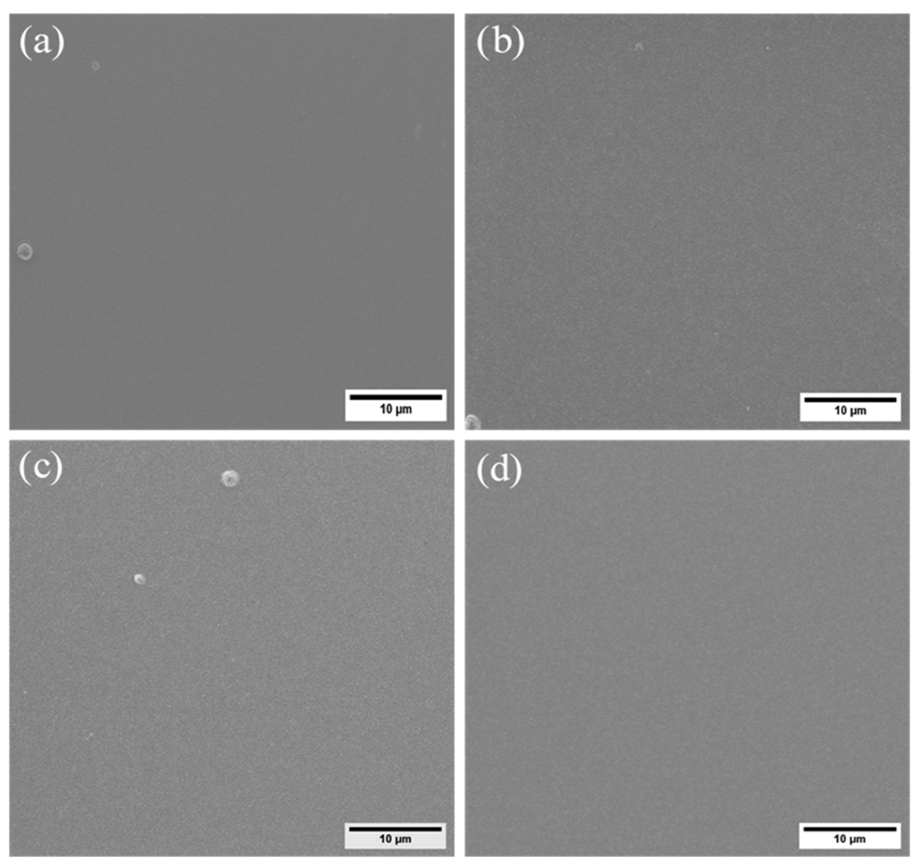
In Figure 1 and Figure 2, the focused ion beam (FIB) metallography images depict the top view and cross-section of the nanotwinned copper (nt-Cu) films sputtered onto silicon carbide (SiC) substrates pre-coated with a chromium (Cr) layer. Figure 1 was measured to ensure the quality of the chip and detect any defects or imperfections on the film’s surface. As a result, it is evident that there are no cracks, pinholes, scratches, or contaminants visible. These films were subjected to varying substrate bias voltages during the deposition process. Notably, when a −100 V substrate bias voltage was applied, the nt-Cu films exhibited a distinctive feature: the persistent presence of large-grain twin crystals, albeit in a significantly reduced proportion. This phenomenon was accompanied by a marked increase in the prevalence of columnar structures, concurrent with a substantial rise in the proportion of nanotwinned grains. Meanwhile, the sputtered Cu without substrate bias, already investigated by [26] showing the polycrystalline copper (Cu) grains, exhibited a uniform distribution across the entirety of the thin film, and no discernible presence of copper nanotwins was detected within the cross-sectional analysis. Upon intensifying the substrate bias voltage to −150 V (Figure 2b), a conspicuous absence of large-grain annealed twin crystals was observed in the copper film. It becomes evident that as the negative substrate bias increased, there was a tendency for the densely stacked nanotwinned columnar grain structures to become more dominant. Consequently, a distinct dual-layered architecture emerged, comprising a lower transition layer and an upper nanotwin layer. The transition layer, characterized by disordered small grains, exhibited relatively greater prominence than the nanotwin layer. This structural configuration remained consistent as the substrate bias voltage was further increased to −200 V, with minimal deviation from the −150 V configuration. This structural trend persisted until the substrate bias voltage reached −250 V. Remarkably, the transition layer notably diminished, while the proportion of columnar grains underwent a discernible increase. However, the nanotwin structures experienced a significant reduction, giving way to larger twin crystals.
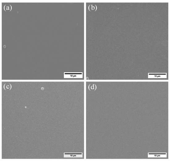
Figure 1.
Top view of FIB metallography of sputtered SiC/Cr/nt-Cu with different biases; (a) −100 V, (b) −150 V, (c) −200 V, and (d) −250 V.
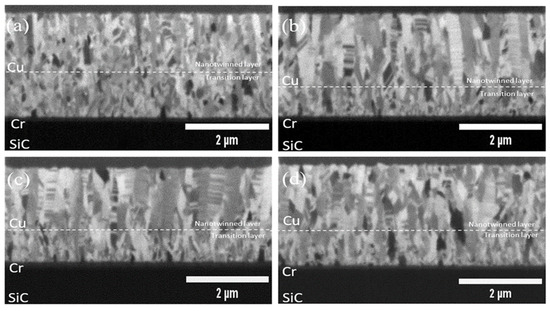
Figure 2.
FIB metallography of the cross-section of sputtered SiC/Cr/nt-Cu with different biases; (a) −100 V, (b) −150 V, (c) −200 V, and (d) −250 V.
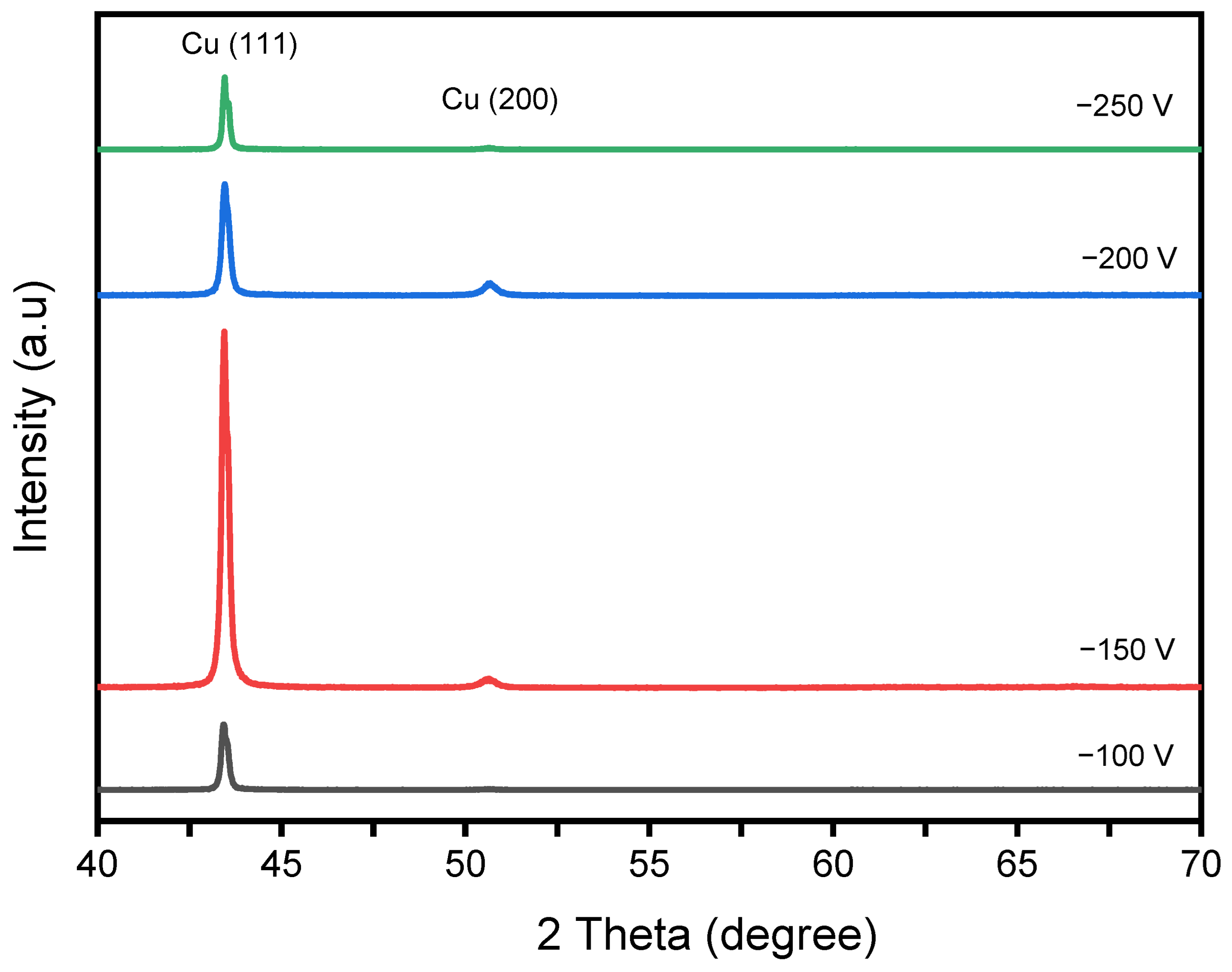
The crystallographic orientation analysis, using X-ray diffraction, highlighted that the copper films deposited across the spectrum of bias voltages predominantly favored a (111) crystal orientation, albeit with significant signal intensity fluctuations. This is illustrated in Figure 3, which underscores the profound influence of applied bias voltage on the signal intensity of the (111) orientation. The peaks of Cu appear at 2theta 43.7° and 50.7°, indicating a (111) and (200) plane, respectively. Crucially, copper films deposited under −150 V exhibited the most robust (111) crystal orientation signal. As the bias voltage surpassed −150 V, the intensity exhibited a gradual decline. However, even in comparison to copper films lacking substrate bias voltage, the (111) orientation signal remained substantially amplified. A supplementary quantitative analysis was performed using electron backscatter diffraction (EBSD) techniques (Figure 4). Furthermore, the application of negative bias voltages to the substrate attracted a multitude of positive ions, precipitating ion bombardment effects. During the process of film deposition, atoms with weak bonding in the film layer experienced sputtering due to the positive ions drawn by the negative bias voltage. This process engendered re-sputtering effects. The escalation of substrate bias voltage corresponded to an augmentation in the energy of incident positive ions, which intensified re-sputtering and, consequently, led to diminished deposition rates.
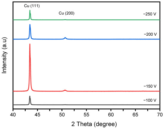
Figure 3.
XRD spectra of Cu nanotwinned films on Cr pre-coated SiC substrates with various biases.
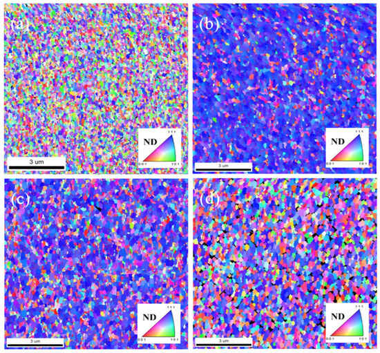
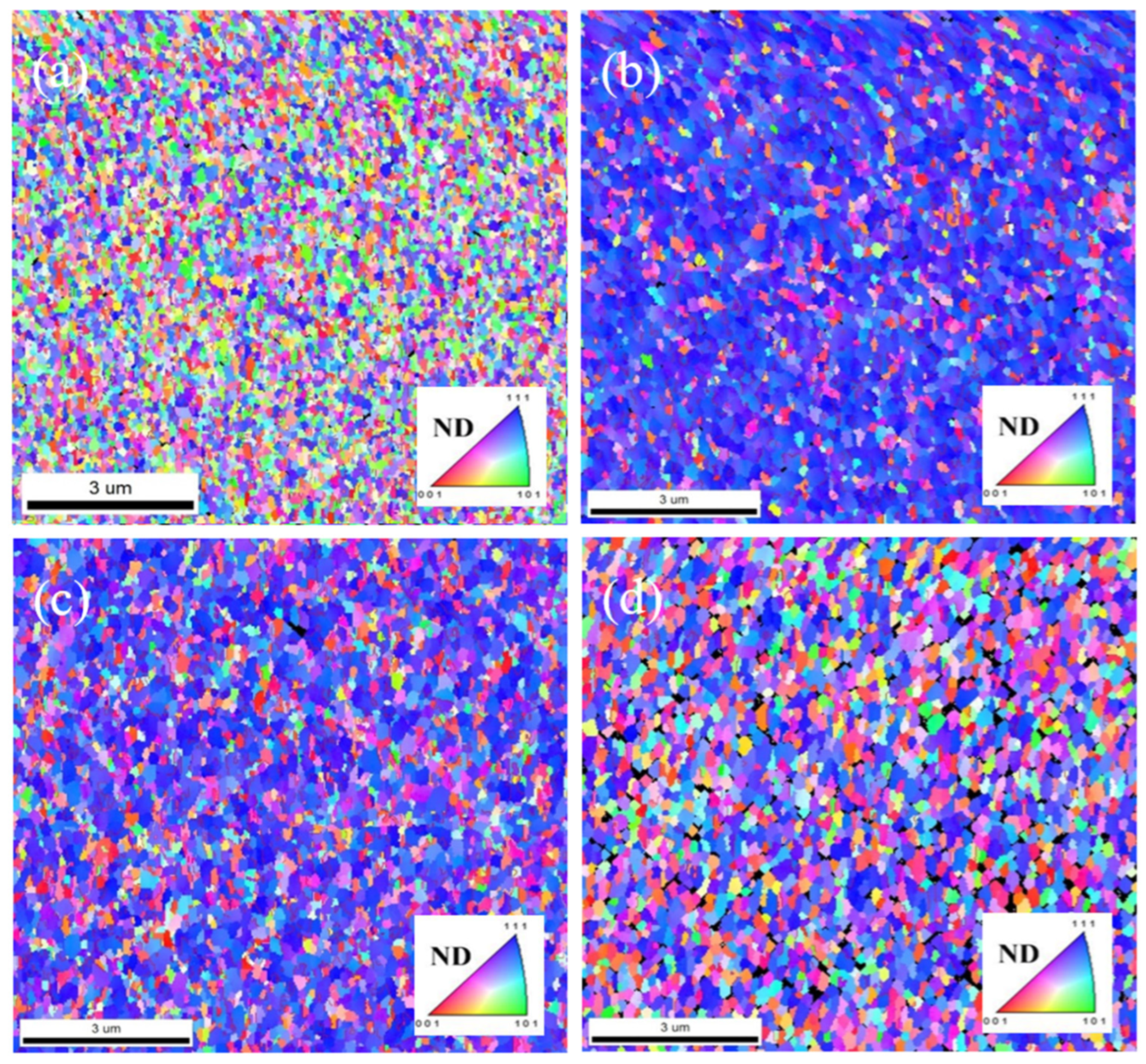
Figure 4.
Top-view EBSD inverse pole figure (IPF) maps of sputtered SiC/Cr/nt-Cu films deposited with substrate biases of (a) −100 V, (b) −150 V, (c) −200 V, and (d) −250 V.
Based on the cross-sectional ion images obtained from FIB, it can be observed that under lower-negative substrate bias, the copper film exhibits a polycrystalline structure. The surfaces of the nanotwinned Cu films must meet a crucial criterion for further bonding applications, that is the percentage of (111) orientation. To further characterize the grain orientations of the Cu thin films, top-view EBSD measurements were conducted and are shown in Figure 4 and Figure 5. The analyses of the proportion of nanotwin boundaries to general grain boundaries within the Cu films are presented in Figure 4a–d. In Figure 4a–d, the conventional grain boundaries are indicated by black lines, and the Σ3 coincident twin boundaries are marked with red lines. The distribution of misorientation angles is used to quantify the proportion of general grain boundaries and CSL-Σ3 twin boundaries. Figure 4a revealed that they comprised 9% Coincidence Site Lattice (CSL-Σ3) boundaries and 2% CSL-Σ9 boundaries in relation to the total grain boundaries, which is the lowest proportion obtained by a substrate bias of −100 V. In contrast, the Cu films depicted in Figure 4b, with a substrate bias of −150 V, exhibited a higher fraction of CSL-Σ3 boundaries, accounting for 33.7% of the total grain boundaries, with only 3.2% attributed to the CSL-Σ9 boundaries. Subsequently, the grain boundary proportion for Figure 4c,d are situated in between.
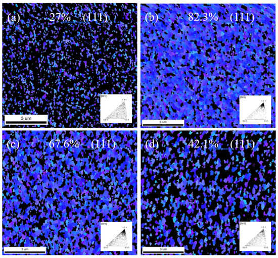
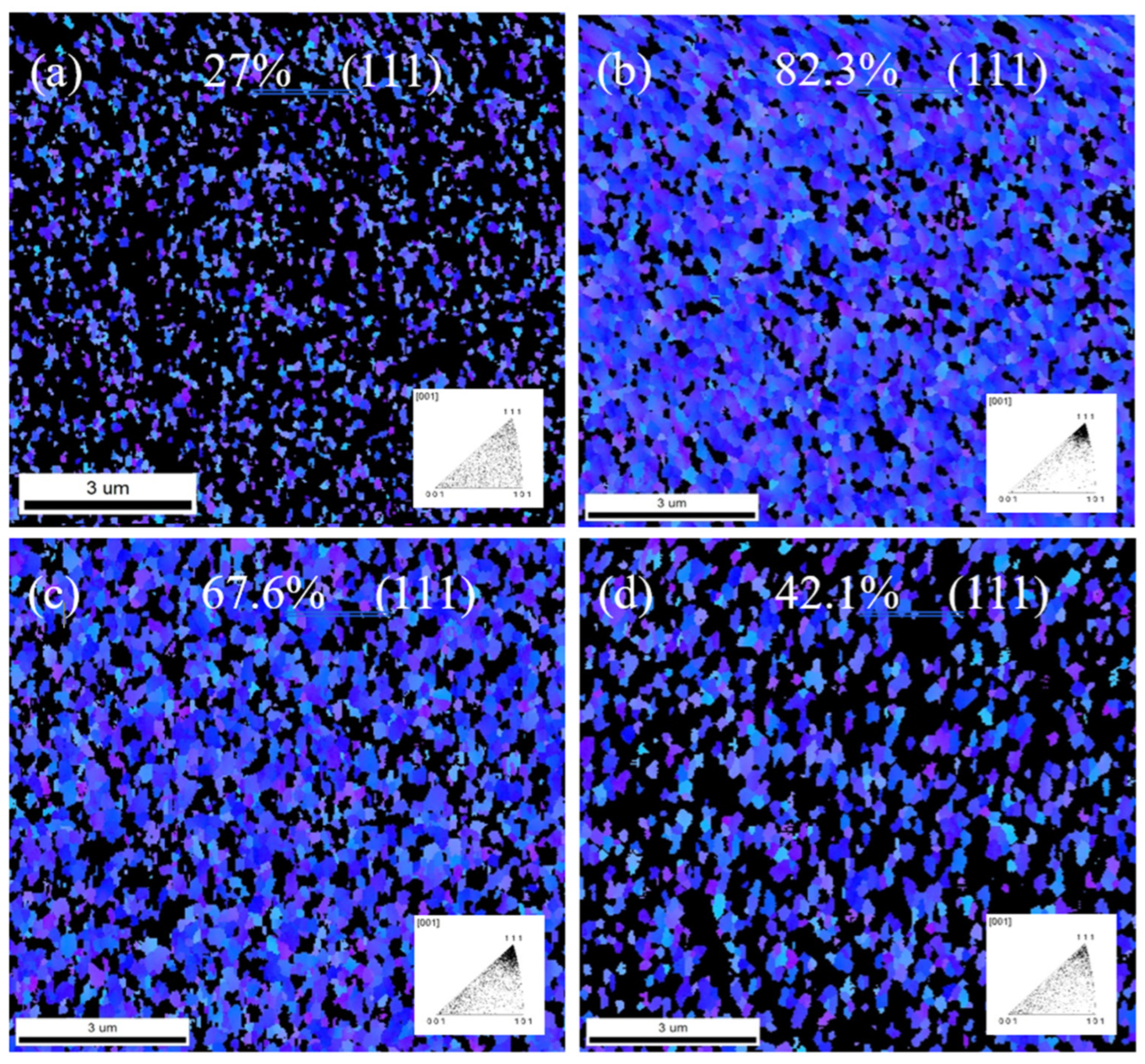
Figure 5.
Plane-view EBSD inverse pole figure (IPF) maps of sputtered Cu films deposited with substrate biases of (a) −100 V, (b) −150 V, (c) −200 V, and (d) −250 V showing (111) orientation.
Figure 5a shows that the (111) proportion is only 27% for bias −100 V. Correspondingly, some nanocrystalline structures begin to emerge on the surface in the cross-sectional ion images. Increasing the bias to −150 V (Figure 5b) leads to a significant increase in the proportion of (111) orientation on the surface, reaching 82.3%. Compared to −100 V (Figure 5a), the overall structure now contains more high-density nanocrystalline structures, with a higher (111) orientation and the copper film exhibits highly ordered columnar nanocrystalline structures. From the plane-view EBSD images, it can be observed that the copper film surface displays a high (111) orientation with a bias of −150 V. This orientation improvement is highly beneficial for future low-temperature bonding. As the substrate bias increases to −200 V, the (111) orientation decreases to 67.6% of the total surface area. However, at −250 V bias, the nanocrystalline structures become less organized compared to −200 V, and the nanocrystalline density significantly decreases. EBSD images reveal that the (111) proportion drops substantially to 42.1%. Based on these results, the quantity of nanocrystalline structures directly affects the proportion of surface (111)-preferred orientation. From the current experimental findings, −150 V is the optimal sputtering parameter, resulting in the highest density of nanocrystalline structures on the overall copper film, along with a highly preferred (111) orientation. This suggests that the substrate bias not only influences the generation and development of sputter deposition structures but also has a significant impact on crystal orientation. These findings underscore the significant influence of substrate bias in facilitating the formation of nanotwins and promoting a <111> crystallographic texture in Cu films. It is worth noting that the high diffusivity characteristic of the Cu (111) plane, in comparison to the (111), (110), and (100) planes, suggests that the application of substrate bias is particularly effective in enhancing bonding quality, leveraging the advantageous properties of the Cu (111) plane.
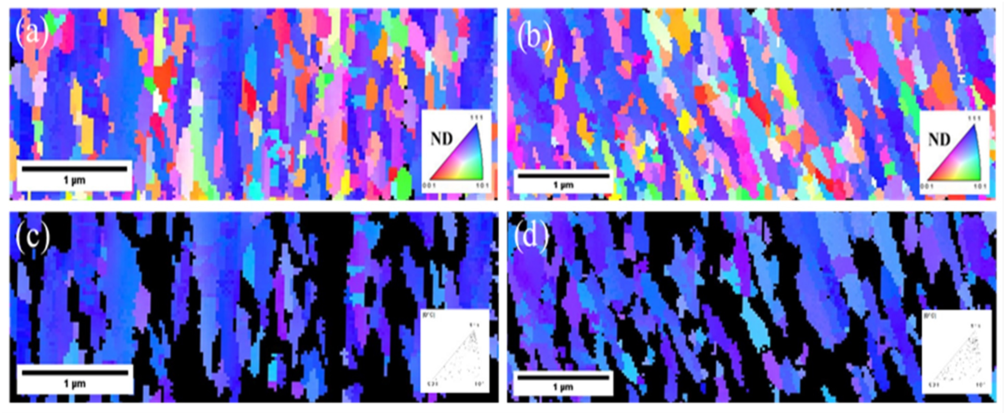
The insights provided in Figure 6 offer a compelling visualization of the predominant growth pattern of columnar copper (Cu) grains, which intriguingly align along the (111) crystallographic direction. This alignment of grain growth along the (111) direction is indicative of a well-defined crystalline orientation preference. Further examination of the data yields noteworthy proportions of certain boundaries within the copper films. Specifically, for the Cu films fabricated on chromium (Cr) pre-coated substrates with substrate biases of −150 V and −200 V; the proportions of Σ3 coincident twin boundaries—a specific type of grain boundary structure—relative to the total grain boundaries are observed to be 49.9% and 42%, respectively. Additionally, the proportions of CSL-Σ9 near twin boundaries—another distinct type of grain boundary configuration—for the substrate biases of −150 V and −200 V amount to 3.1% and 2.6%, respectively. These findings imply that the Cu film cultivated under the bias of −150 V exhibits the highest twin density in terms of these specific boundaries. This result corroborates the earlier observations from the cross-sectional metallography depicted in Figure 2a–d.
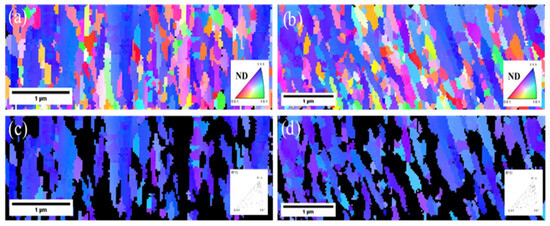
Figure 6.
EBSD analyses of the cross-section of sputtered Cu nanotwinned films on SiC substrate with the Cr pre-coating EBSD inverse pole figure mapping (a) −150 V; (b) −200 V; EBSD (111) grain mapping (c) −150 V; (d) −200 V.
Moreover, the study ventures further to analyze the distribution of other grains within the Cu film that deviates from the [111] direction by more than 15°. These distinct grains are represented as black regions in Figure 6c,d. This analysis underlines the selective prevalence of the (111) orientation across the nanotwinned Cu film surface. Specifically, it becomes apparent that 61.4% of the nanotwinned Cu film surface maintains the (111) orientation when grown under the −150 V bias condition. In comparison, the bias condition of −200 V yields a slightly reduced prevalence of the (111) orientation, with only 60.4% of the surface adhering to this crystallographic orientation.
These nuanced observations accentuate the intricate interplay between substrate bias, crystalline orientations, and grain boundary structures within the fabricated copper films. The high twin density exhibited by the Cu film grown under −150 V bias further substantiates the influence of bias conditions on crystallographic orientations and the associated grain boundary configurations. This understanding is pivotal in optimizing the synthesis of materials with desired microstructural attributes, which subsequently impact their mechanical, electrical, and thermal properties for various applications.
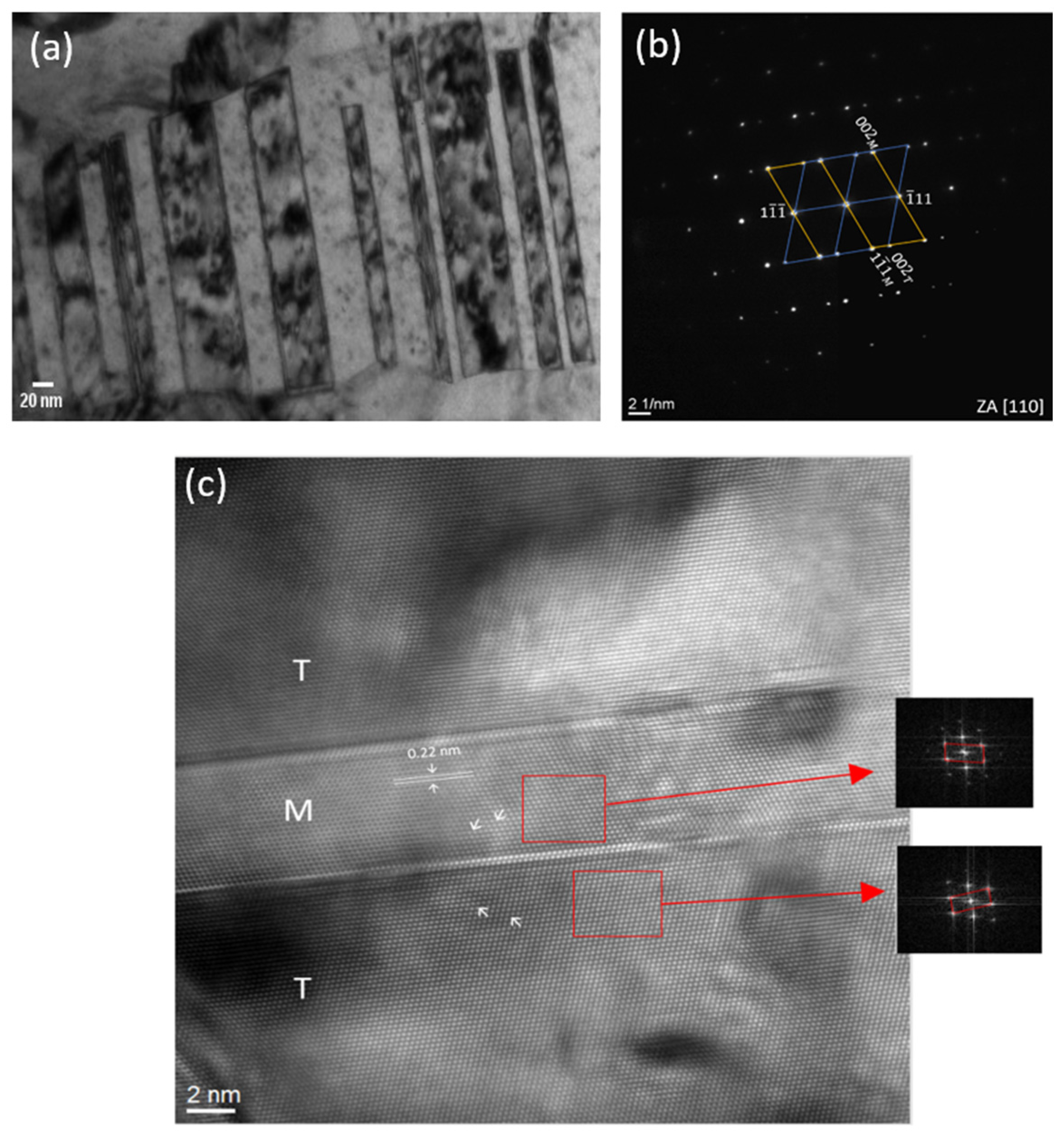
In addition to the examination of FIB and EBSD cross-sections, the microstructure was further scrutinized using transmission electron microscopy (TEM). Figure 7 displays cross-sectional TEM bright-field images and high-resolution TEM (HRTEM) images of the Cu film with a −150 V bias during deposition. In Figure 7a, a notably dense nanotwinned structure is evident, signifying a predominant (111)-preferred orientation in most columnar grains. The selected area diffraction (SAD) pattern, captured along the [110] zone axis in Figure 7b, reveals distinct diffraction spots belonging to the matrix (M) and twins (T) within the columnar grains from Figure 7a. These spots symmetrically align along the (111)/(111) co-plane, providing clear evidence of a twin structure. Furthermore, Figure 7c displays a high-resolution TEM (HRTEM) image and a fast Fourier transform (FFT) pattern of twins and the matrix. These results demonstrate the alternating stacking of nanotwins and the matrix. Additionally, the Cu (111) twin boundaries in Figure 7c reveal an exceedingly fine atomic spacing of approximately 0.22 nm.

Figure 7.
Cross-sectional TEM micrographs of as-deposited Cu nanotwinned film deposited with −150 V bias: (a) bright-field TEM image of columnar Cu nanotwin, (b) diffraction pattern taken along the [110] zone axis, and (c) high-magnification HRTEM image of nanotwinned structures with different fast Fourier transformation (FFT) patterns of twin and matrix.
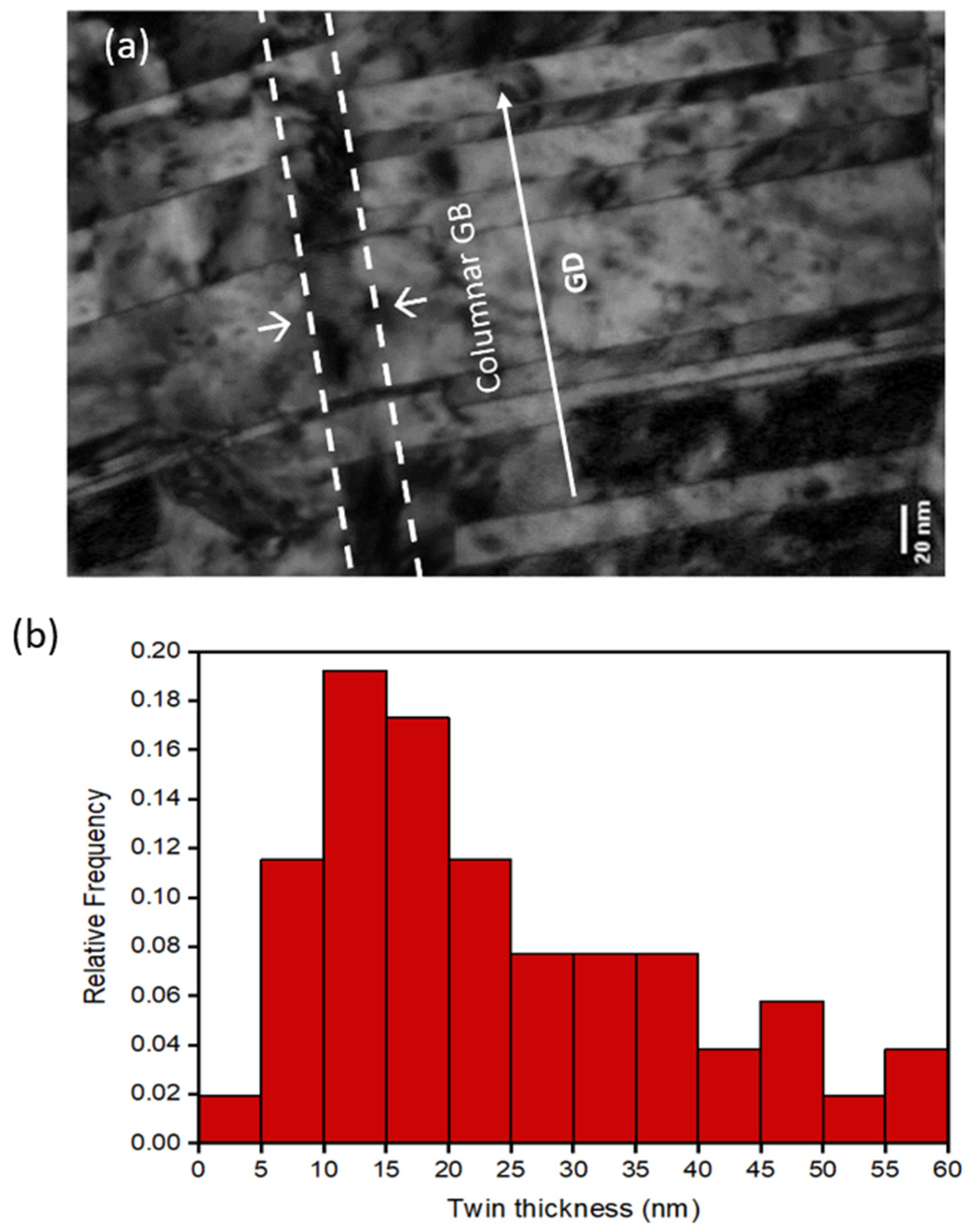
Furthermore, Figure 8a presents a bright-field image illustrating two columnar grain structures composed of densely packed Cu nanotwins stacked atop one another along the growth direction (GD). The densely stacked nanotwins are prominently observed along the columnar grains. The nanotwin thickness distribution is depicted in Figure 8b, with the majority falling within the range of 10 to 25 nm and an average twin thickness of 24.1 ± 14 nm.

Figure 8.
(a) Cross-sectional bright-field TEM image of area between columnar grains and (b) distribution of twin thicknesses in the highly (111)-oriented Cu film.
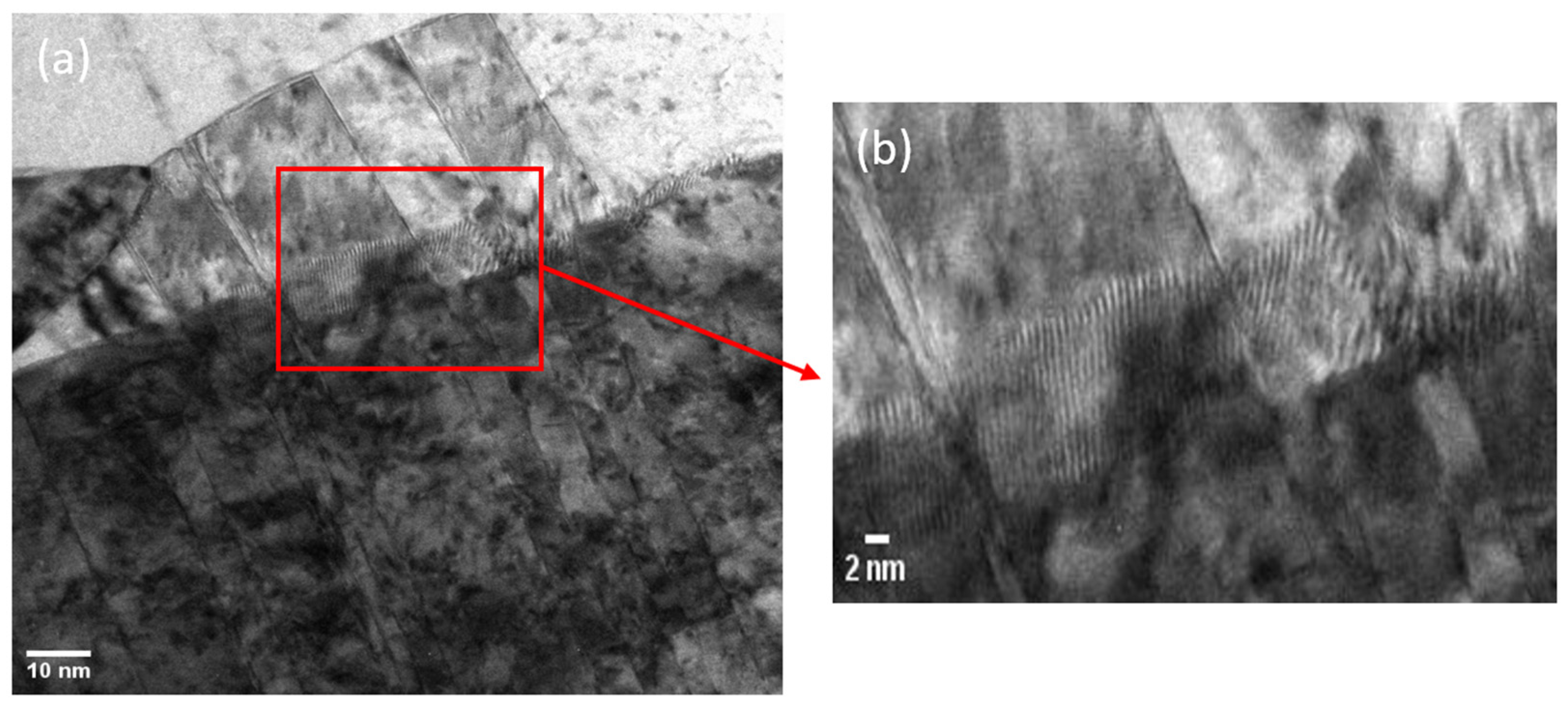
It is noteworthy that exceedingly fine lamellar structures have been observed at the interface between nanotwinned columnar grains, as illustrated in Figure 9. The spacing between these fine lamellae measures is less than 1 nm. In accordance with the Cu–Cr phase diagram presented by Chakrabarti and Laughlin [27], the solubility of Cr in Cu is found to be less than 0.1 at.%. Consequently, it is postulated that a limited number of Cr atoms within the adhesive layer diffuse along the interface between nanotwinned columnar grains, leading to grain boundary migration and the decomposition of the Cr–Cu solid solution into discontinuous precipitates (DP). This phase decomposition results in the formation of sub-nanometer-sized DP lamellar cells at the nanotwinned columnar grain boundaries. The occurrence of this diffusion-induced sub-nano-sized lamellar precipitation within nanotwins has never been reported and is currently under further investigation in our laboratory.

Figure 9.
(a,b) Cross-sectional bright-field TEM image reveals the presence of fine lamellar cells at the interface between the nanotwinned columnar grains.
4. Discussion
The bias voltage applied to the substrate has a direct impact on the energy of ions during their bombardment of the surface where thin film growth takes place as the results above. Consequently, this deposition parameter is expected to exert a substantial influence on the microstructure of the thin film as it is initially deposited. Higher substrate bias voltages lead to increased levels of compressive stress, enhanced surface mobilities, greater implantation of impinging particles, and increased displacement of lattice atoms. These factors collectively facilitate the introduction of additional stacking faults, which then accumulate and evolve into twin boundaries within the material. A thermodynamic model predicts that a higher deposition rate, often achieved through elevated target power, enhances the likelihood of the formation and growth of these twinned nuclei in the thin film [15].
Nonetheless, the present investigation does not exhibit this phenomenon. Instead, a greater prevalence of nanotwin structures is evident in the coating deposited at a lower deposition rate. While the precise underlying factors for this observation remain ambiguous, it is hypothesized that the mechanisms governing film growth and twin formation during magnetron sputtering are subject to kinetic control. Consequently, the applicability of the thermodynamic model in comprehensively elucidating this behavior is constrained [26]. In practical terms, the process of film growth during magnetron sputtering is primarily governed by kinetics, rendering it challenging to provide a comprehensive description solely through thermodynamic models. While the thermodynamic model mentioned in the preceding section suggests that elevated deposition rates should result in increased twin density, multiple experimental studies have contradicted this prediction. Moreover, alterations in twin spacing are often concurrent with shifts in grain size. These challenges arise from the interdependence of adatom kinetic energy and flux, both of which significantly influence the film growth process and rates of twin formation. Unfortunately, these factors are inherently linked to the same tunable sputtering parameters, rendering independent control challenging [28].
Additionally, the Cr interlayer can reduce the coefficient of thermal expansion (CTE) mismatch between the Cu–SiC substrate and can smooth the difference in lattice parameters at the interface by effectively absorbing some of this differential expansion, acting as a buffer zone. Zi Hong and coworkers have reported that the Cu nanotwinned thin film produced through sputtering and subjected to surface activation displayed a thinner transition layer. This layer consisted of randomly oriented grains, potentially serving as a structural weak point that could compromise the uniformity of the nanotwinned films. In contrast, the Cu nanotwinned thin film sputtered without surface activation and exhibited a thicker transition layer [29].
Chromium can create strong chemical bonds with both the Cu layer and the SiC film as an adhesion layer [30]. This characteristic enhances the adhesion between the Cu layer and the SiC substrate, preventing the Cu film from delaminating or peeling. It acts as a barrier layer, preventing atoms from diffusing between the Cu layer and the SiC substrate. At elevated temperatures, copper has a tendency to diffuse into silicon-based materials such as SiC, which can cause material degradation and device failure. Thus, the Cr adhesion layer inhibits diffusion and preserves the structure’s integrity. As a result, the Cr interlayer creates a transitional region where the lattice parameters gradually change from those of SiC to those of Cu. This gradual transition reduces abrupt changes at the Cu–SiC interface, minimizing stress and defects.
The application of a suitably biased substrate is also recognized for its capacity to enhance the adhesive properties of magnetron-sputtered coatings. This improvement stems from the additional energy made available to the growing film, as high-energy atoms tend to migrate towards low-energy sites on the surface to optimize their adhesion characteristics. This phenomenon was prominently observed in the samples subjected to substrate bias due to the multifaceted advantages it confers. When a negative substrate bias voltage was employed during deposition, it led to the attraction of Ar+ ions for the bombardment of the films. As the magnitude of the applied negative substrate bias increased, a greater number of Ar+ ions possessing higher energy levels were drawn in to bombard the films, thereby altering the translational kinetic energy of the adatoms. As these high-energy Ar+ ions collided with the surface atoms of the films, the mobility of the atoms was augmented, resulting in a reduction in the formation of voids and the development of finer faceted columns.
It is evident that the film deposited with substrate bias, as depicted in Figure 2b, exhibited finer and more densely packed faceted columns, with a concurrent reduction in the thickness of the transition region. Zi Hong et al. (2023) conducted a sputtered Cu nanotwinned film without the surface activation layer and exhibited an average twin thickness of 45.8 nanometers [29]. The findings demonstrated that subjecting the surface to Ar ion bombardment prior to sputtering proved to be an effective means of reducing twin thickness and elevating the density of the nanotwins [29,31]. This refinement and densification of the grains typically correlates with an increase in the hardness of the coatings. Furthermore, as the grains were refined to the nanoscale, a greater number of grain boundaries and free surfaces characterized by higher energy levels were generated, creating more nucleation sites for the formation of nanotwins. From the aforementioned discussion, it can be deduced that the addition of substrate bias, when appropriately applied, results in the densification and improved lattice arrangement of the crystal structure. This, in turn, promotes the nucleation of nanotwins, characterized by a higher proportion of (111) crystal orientation, as depicted in Figure 5b. In essence, this process swiftly transforms copper thin films into a nanotwinned columnar layer, thereby enhancing the overall film quality.
5. Conclusions
In this investigation, the influence of varying substrate biases on the microstructural and crystallographic characteristics of copper (Cu) films was systematically examined. The observed augmentation in nanotwin formation is believed to be attributed to ion bombardment and the presence of a chromium (Cr) adhesive layer. Notably, the Cu film sputtered with a substrate bias of −150 V demonstrated better properties, with a thinner transition layer and higher twin density with relatively thin twin thickness. The crystallographic orientation analysis using X-ray diffraction highlighted that copper films deposited across the spectrum of bias −150 V predominantly favored a (111) crystal orientation with relatively highest intensity. Increasing the bias to −150 V leads to a significant increase in the proportion of (111)-preferred orientation on the plane-view of the EBSD image, reaching 82.3%, and more ordered columnar nanocrystalline structures, as shown in the FIB cross-section. Additionally, the nanotwin thickness distribution mostly falls within the range of 10 to 25 nm and an average twin thickness of 24.1 ± 14 nm. These were characterized by a high density of Cu nanotwinned structures predominantly oriented along the (111) crystallographic plane. This particular nanotwinned film exhibits the potential to enhance the performance of backside metallization processes.
Author Contributions
Conceptualization, T.-H.C. and M.-T.C.; data curation, D.I.S., M.-T.C. and T.-H.C.; investigation, T.-H.C. and M.-T.C.; methodology, M.-T.C. and T.-H.C.; writing—original draft, D.I.S.; writing—review and editing, D.I.S.; supervision, T.-H.C.; project administration, T.-H.C. All authors have read and agreed to the published version of the manuscript.
Funding
This study was sponsored by the Emerging Technology Application Program of the Hsinchu Science Park R & D program of Ag Materials Technology Co., Ltd. under Grant No. 112AO03A.
Data Availability Statement
Not applicable.
Conflicts of Interest
The authors declare no conflict of interest in any capacity, competing or financial.
References
- Thompson, S.; Parthasarathy, S. Moore’s Law: The future of Si microelectronics. Mater. Today 2006, 9, 5–20. [Google Scholar] [CrossRef]
- Jiang, N.; Liu, H.; Zou, J.; Guo, C.; Li, W.; Shi, M.; Yang, B.; Liu, Y.; Guo, B. Packaging design for improving the uniformity of Chip scale package (CSP) LED luminescence. Microelectron. Reliab. 2021, 122, 114136. [Google Scholar] [CrossRef]
- Kumar, S. Fundamental Limits to Moore’s Law. arXiv 2015. [Google Scholar] [CrossRef]
- Kandlikar, S.G.; Ganguly, A. Fundamentals of Heat Dissipation in 3D IC Packaging and Thermal-Aware Design. 3D Microelectron. Packag. 2021, 64, 369–395. [Google Scholar]
- Liang, Z.; Ning, P.; Wang, F. Development of advanced all-sic power modules. IEEE Trans. Power Electron. 2014, 29, 2289–2295. [Google Scholar] [CrossRef]
- Neeb, C.; Boettcher, L.; Conrad, M.; de Doncker, R.W. Innovative and reliable power modules: A future trend and evolution of technologies. IEEE Ind. Electron. Mag. 2014, 8, 6–16. [Google Scholar] [CrossRef]
- Lu, L.; Chen, X.; Huang, X.; Lu, K. Revealing the Maximum Strengthin Nanotwinned Copper. Science 2009, 323, 603–607. [Google Scholar] [CrossRef]
- Zhang, X.; Misra, A. Superior thermal stability of coherent twin boundaries in nanotwinned metals. Scr. Mater. 2012, 66, 860–865. [Google Scholar] [CrossRef]
- Chen, K.J.; Wu, J.A.; Chen, C. Effect of Reverse Currents during Electroplating on the (111)-Oriented and Nanotwinned Columnar Grain Growth of Copper Films. Crystal Growth and Design. 2020, 20, 3834–3841. [Google Scholar] [CrossRef]
- Detavernier, C.; Deduytsche, D.; Van Meirhaeghe, R.; De Baerdemaeker, J.; Dauwe, C. Room-temperature grain growth in sputter-deposited Cu films. Appl. Phys. Lett. 2003, 82, 1863–1865. [Google Scholar] [CrossRef]
- Tong, X.; You, G.; Ding, Y.; Xue, H.; Wang, Y.; Guo, W. Effect of grain size on low-temperature electrical resistivity and thermal conductivity of pure magnesium. Mater. Lett. 2018, 229, 261–264. [Google Scholar] [CrossRef]
- Yeap, K.H.; Nisar, H.; Dakulagi, V. Warpage reduction for power mosfet wafers. Electrica 2021, 21, 173–179. [Google Scholar] [CrossRef]
- Xie, Y.; Wang, Q.; Han, L.; Wu, D. Study on Ion Bombardment Semiconductor Shaped Self-Assembled Nanostructures. Acad. J. Mater. Chem. 2023, 4, 4. [Google Scholar]
- Zhang, X.; Misrah, A.; Wang, H.; Nastasi, M.; Embury, J.; Mitchell, T.; Hongland, R.; Hirth, J. Nanoscale-twirming-induced strengthening in austenitic stainless steel thin films. Appl. Phys. Lett. 2004, 84, 1096–1098. [Google Scholar] [CrossRef]
- Zhang, X.; Misrah, A.; Wang, H.; Shen, T.; Nastasi, M.; Mitchell, T.; Hirth, J.; Hongland, R.; Embury, J. Enhanced hardening in Cu/330 stainless steel multilayers by nanoscale twinning. Acta Mater. 2004, 52, 995–1002. [Google Scholar] [CrossRef]
- Zhang, X.; Wang, H.; Chen, H.; Lu, L.; Lu, K.; Hoagland, R.G.; Misra, A. High-strength sputter-deposited Cu foils with preferred orientation of nanoscale growth twins. Appl. Phys. Lett. 2006, 88, 17. [Google Scholar] [CrossRef]
- Anderoglu, O.; Misra, A.; Wang, H.; Ronning, F.; Hundley, M.; Zhang, X. Epitaxial nanotwinned Cu films with high strength and high conductivity. Appl. Phys. Lett. 2008, 93, 8. [Google Scholar] [CrossRef]
- Bufford, D.; Bi, Z.; Jia, Q.; Wang, H.; Zhang, X. Nanotwins and stacking faults in high-strength epitaxial Ag/Al multilayer films. Appl. Phys. Lett. 2012, 101, 22. [Google Scholar] [CrossRef]
- Hodge, A.M.; Wang, Y.; Barbee, T.W. Mechanical deformation of high-purity sputter-deposited nano-twinned copper. Scr. Mater. 2008, 59, 163–166. [Google Scholar] [CrossRef]
- Hodge, A.M.; Wang, Y.; Barbee, T.W. Large-scale production of nano-twinned, ultrafine-grained copper. Mater. Sci. Eng. A 2006, 429, 272–276. [Google Scholar] [CrossRef]
- Shute, C.J.; Myers, B.D.; Xie, S.; Li, S.Y.; Barbee, T.W., Jr.; Hodge, A.M.; Weertman, J.R. Detwinning, damage and crack initiation during cyclic loading of Cu samples containing aligned nanotwins. Acta Mater. 2011, 59, 4569–4577. [Google Scholar] [CrossRef]
- Wang, Y.M.; Sansoz, F.; Lagrange, T.; Ott, R.; Marian, J.; Barbee, T.; Hamza, A. Defective twin boundaries in nanotwinned metals. Nat. Mater. 2013, 12, 697–702. [Google Scholar] [CrossRef]
- Lagrange, T.; Reed, B.W.; Wall, M.; Mason, J.; Barbee, T.; Kumar, M. Topological view of the thermal stability of nanotwinned copper. Appl. Phys. Lett. 2013, 102, 1. [Google Scholar] [CrossRef]
- Khanna, V.K. Adhesion-delamination phenomena at the surfaces and interfaces in microelectronics and MEMS structures and packaged devices. J. Phys. D Appl. Phys. 2011, 44, 3. [Google Scholar] [CrossRef]
- Teng, P.; Li, X.; Hua, P.; Liu, H.; Wang, G. Effect of metallization temperature on brazing joints of SiC ceramics and 2219 aluminum alloy. Int. J. Appl. Ceram Technol. 2022, 19, 498–507. [Google Scholar] [CrossRef]
- Yang, Z.H.; Wu, P.; Chuang, T.H. Effects of substrate bias on the sputtering of high density (111)-nanotwinned Cu films on SiC chips. Sci. Rep. 2022, 12, 1. [Google Scholar]
- Chakrabarti, D.J.; Laughlin, D.E. The Cr-Cu (Chromium-Copper) System. Bull. Alloy. Phase Diagr. 1984, 5, 59–68. [Google Scholar] [CrossRef]
- Bufford, D.C.; Wang, Y.; Liu, Y.; Lu, L. Synthesis and microstructure of electrodeposited and sputtered nanotwinned face-centered-cubic metals. MRS Bull. 2016, 41, 286–291. [Google Scholar] [CrossRef]
- Yang, Z.H.; Chen, Y.; Chuang, T.H. Growth of Cu nanotwinned films on surface activated SiC chips. J. Mater. Sci. Mater. Electron. 2023, 34, 23. [Google Scholar] [CrossRef]
- Ishibashi, R.; Ishida, K.; Kondo, T.; Watanabe, Y. Corrosion-resistant metallic coating on silicon carbide for use in high-temperature water. J. Nucl. Mater. 2021, 557, 153214. [Google Scholar] [CrossRef]
- Leh, P.C.; Wang, J.; Fan, Y.O. Improvement of Ag films with highly (111) surface orientation for metal direct bonding technique: Nanotwinned structure and ion bombardment effect. Mater. Chem. Phys. 2021, 274, 125159. [Google Scholar]

Disclaimer/Publisher’s Note: The statements, opinions and data contained in all publications are solely those of the individual author(s) and contributor(s) and not of MDPI and/or the editor(s). MDPI and/or the editor(s) disclaim responsibility for any injury to people or property resulting from any ideas, methods, instructions or products referred to in the content. |
© 2023 by the authors. Licensee MDPI, Basel, Switzerland. This article is an open access article distributed under the terms and conditions of the Creative Commons Attribution (CC BY) license (https://creativecommons.org/licenses/by/4.0/).