Article

Influence of Pretreatment Processes on Adhesion of Ni/Cu/Ni Multilayer on Polyetherimide Resin Reinforced with Glass Fibers

1
Electrochemistry and Corrosion Laboratory, School of Mechanical Engineering and Rail Transit, Changzhou University, Changzhou 213164, China
2
Jiangsu Kexiang Anticorrosive Materials Co., Ltd., Changzhou 213100, China
3
Zhenjiang Arf Special Coating Technology Co., Ltd., Zhenjiang 212006, China
*
Author to whom correspondence should be addressed.
Metals 2022, 12(8), 1359; https://doi.org/10.3390/met12081359
Submission received: 8 July 2022 / Revised: 12 August 2022 / Accepted: 13 August 2022 / Published: 16 August 2022
(This article belongs to the Special Issue Special Metal-Alloy Coating and Catalysis)

Abstract

:
The metallization of polyetherimide (PEI) is widely considered to enhance its surface properties and enhance its application in engineering fields; however, adhesion is a key factor in determining the reliability of PEI metallization. A Ni/Cu/Ni multilayer coating was successfully manufactured on a batch of PEI resin reinforced with glass fibers by a two-step metallization process, including sandblasting and activation/acceleration. The microstructure and morphology of the top-surface and cross-section of the coatings were observed by scanning electron microscopy. The chemical state and composition of the deposits were characterized by both X-ray photoelectron and energy-dispersive spectroscopy. The adhesion state was qualitatively evaluated by cross-cut tests with 3M tape. The surface roughness of the substrate significantly increased after the sandblasting process, which could improve the adhesion between the multilayer coating and the PEI substrate. After the standard activation process, the acceleration made an effect on the deposition of the initial Ni layer for electroless plating. The influence of acceleration on the appearance quality of metallization on the PEI substrate was studied and, at the same time, the mechanism of acceleration was investigated and addressed.

1. Introduction

Currently, the surface metallization of polymeric substrates, with or without fiber reinforcement, is a study area of growing interest because of the need to enhance their surface properties. In fact, the polymer-based materials are increasingly used in several sectors of engineering, such as automotive, aerospace, and construction, replacing metals for different applications [1]. Polyetherimide (PEI)-based materials are amorphous, thermoplastic polymers, which are chemically stable, biocompatible, and exhibit the mechanical, thermal, and dielectric properties required for next-generation applications [2]. PEI-based materials have some advantages, such as high heat resistance, stiffness, impact strength, high mechanical strength and flame resistance, and broad chemical resistance [3,4]. PEI could offer advantages such as lightness, a high strength to weight ratio, and flexibility in designing shapes and forms. On the other hand, it could also be useful to improve some of its properties, such as its electrical conductivity, electromagnetic shielding capabilities, thermal conductivity, flame resistance, and erosion and radiation protection, in order to further widen the fields of application for PEI-based materials. In this regard, the surface metallization of the PEI substrate is an effective technique to enhance the above-mentioned surface properties to expand their engineering applications [5].
Some approaches could be used to prepare a metallic layer on the polymers, such as physical (PVD) [6,7] and chemical vapor deposition (CVD) [8,9], the use of thermal [10] and cold spray [1,11], using electroless plating [12,13,14], and electroplating a conductive layer [15]. PVD, CVD, and spray techniques incur high equipment and processing costs, and are limited in terms of productivity and workpiece sizes and shapes. Electroless plating is an alternative way to produce the metallic layer on PEI composite substrates when plating without applied current and vacuum conditions or using a low bath temperature, and has applicability to complicated-shaped substrates [16,17,18,19]. Electroless nickel plating on polyethylene terephthalate surfaces for triboelectric nanogenerators facilitates the improvement of device wearability and comfort [20]. Marques-Hueso et al. [21] reported that a rapid photosynthesis method was used to produce the silver nanoparticles on PEI substrates. Marline et al. [22] studied a direct metallization of Ni coating on PEI substrates by spin-coating or a dipping deposition of an ultra-thin film of an organic nickel salt in an alcoholic solution. Jones et al. [23] investigated a direct metallization of PEI substrates by activation with metal ions as seed layers, which could be reduced and formed by chemical or optical reduction. Alodan [24] reported a metallizing PEI resin reinforced with glass fibers, where the surface of the PEI substrate was modified by etching the resin matrix and the glass fibers using two different solutions. During the resin etching step, glass fibers were exposed and etched at the surface. Glass fiber etching was found to be essential to promote adhesion between the metallic film and the PEI surface. After electroplating, the adhesion force was 230 kg/cm2 (3000 psi). Esfahani et al. [2] presented a new digital fabrication strategy that combined the 3D printing of high-performance polymers (polyetherimide) with a light-based selective metallization of copper traces through the chemical modification of the polymer surface and the computer-controlled assembly of functional devices and structures. Zhang et al. [25] reported that a new surface modification method was developed for the electroless deposition of robust metal (copper, nickel, silver, etc.) layers on a poly(dimethylsiloxane) substrate with strong adhesion.
Adhesion strength is an important parameter in determining the reliability of the metallization of the PEI substrates [26]. In fact, it is hard to obtain a strong adhesion between the layer and the PEI substrate due to high interfacial energy. Some pretreatment processes could be helpful to improve the adhesion strength, including laser [27,28,29], plasma [30,31], and mechanical roughening [32,33], as well as chemical etching [34,35]. These pretreatment processes increase the surface roughness, and wettability or chemical bonding of the substrates, resulting in a strong adhesion between the metallic layer and the substrate. For conventional electroless plating, adsorbed palladium (Pd) catalysts are widely used to activate the surface for the following electroless metallization. The sensitization/activation and acceleration could seed a catalyst on the surface of the PEI substrates for electroless plating, which could also influence the adhesion of the metallic layer. Pretreatment of the PEI substrate with the PdCl/SnCl sensitizer solution leads to the adsorption of catalytically inactive Sn and Pd compounds or complexes [36]. Subsequently, the excess tin oxides, hydroxides, and salts were removed by an accelerator solution, and then the active catalyst species consisted of left behind metallic Pd and PdSn particles approximately 1–10 nm in size, which become the deposition center of Ni atoms for electroless plating. However, there are few reports on the influence of pretreatment processes, including mechanical sandblasting and acceleration, on the adhesion of the metallization of PEI substrates. Generally, the deposition of electroless plating on PEI substrates required a chemical pretreatment to ensure good adhesion; however, there are limitations due to its low adhesive strength and a long production cycle strongly linked to environmental hazards/costs. [34,35].
In a recent publication, a composite coating of a Ni/Cu/Ni multilayer was produced on the surface of PEI reinforced with glass fiber composite substrates. Ni and Cu layers were obtained by electroless plating and electrodeposition, respectively. The influences of the Cu interlayer thickness and heat treatment on the adhesion state of the multilayer coatings on the substrate were studied [32]. Film thickness has an important effect on adhesion. The adhesion solution of the Ni/7.54 µm Cu/Ni and Ni/58.6 µm Cu/Ni multilayers on PEI composites could be classified as grade 5B and 3B, respectively. Furthermore, the adhesion force of the Ni/58.6 µm Cu/Ni multilayer on the substrate can be improved by heat treatment at 200 °C for 4 h. However, the pretreatment processes for metallization on PEI substrates play a key factor on the adhesion and appearance quality of the deposits. In this study, a coating of Ni/Cu/electroless Ni multilayer was deposited on PEI reinforced with the glass fibers. Therefore, it is necessary to study the effect of pretreatment processes, such as roughening and acceleration processes, on the adhesion of the Ni/Cu/Ni multilayer on PEI composite substrates. Tape peel tests were used to determine the adhesion state of Ni/Cu/Ni/PEI composites with pretreatment processes.

2. Experimental Section

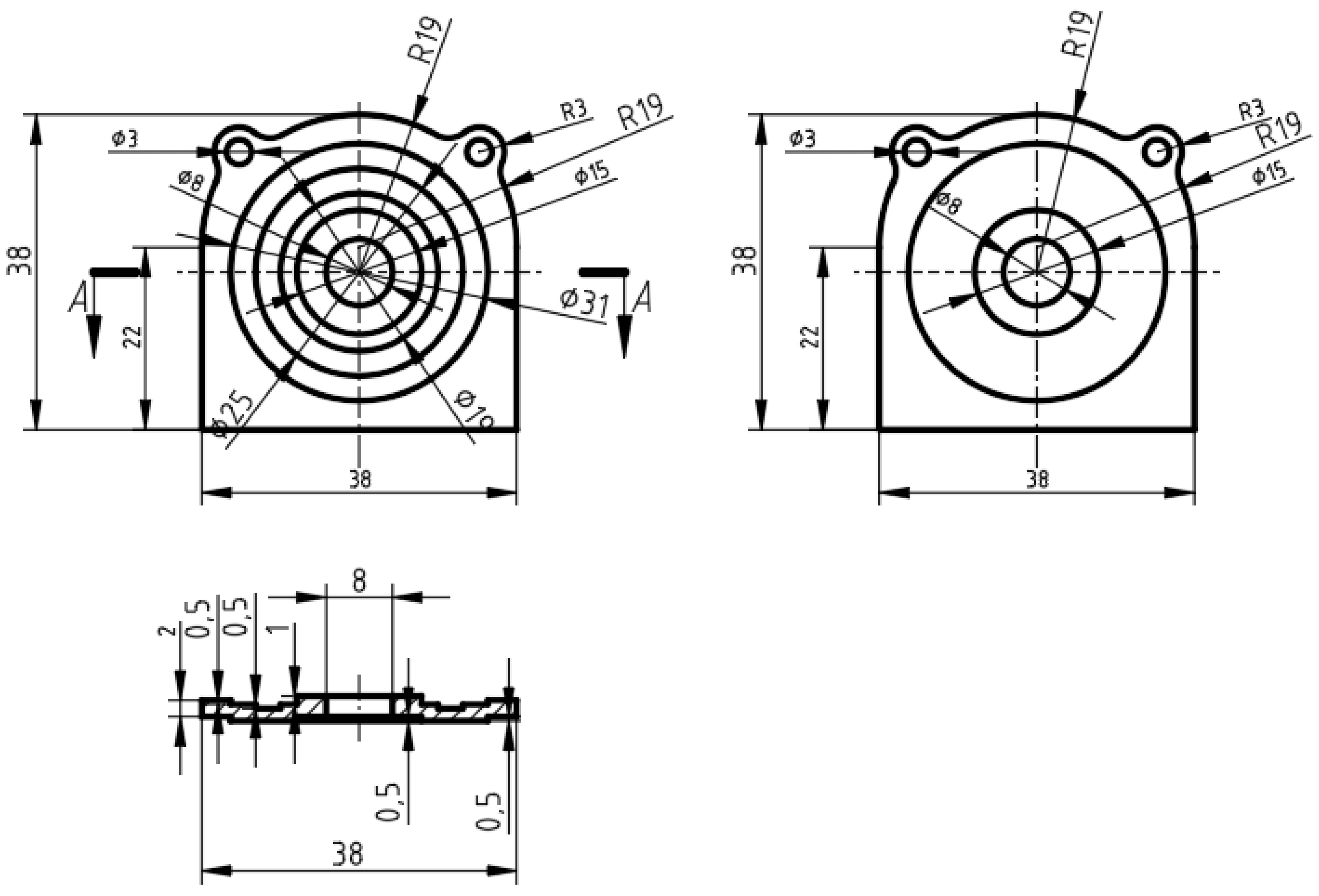
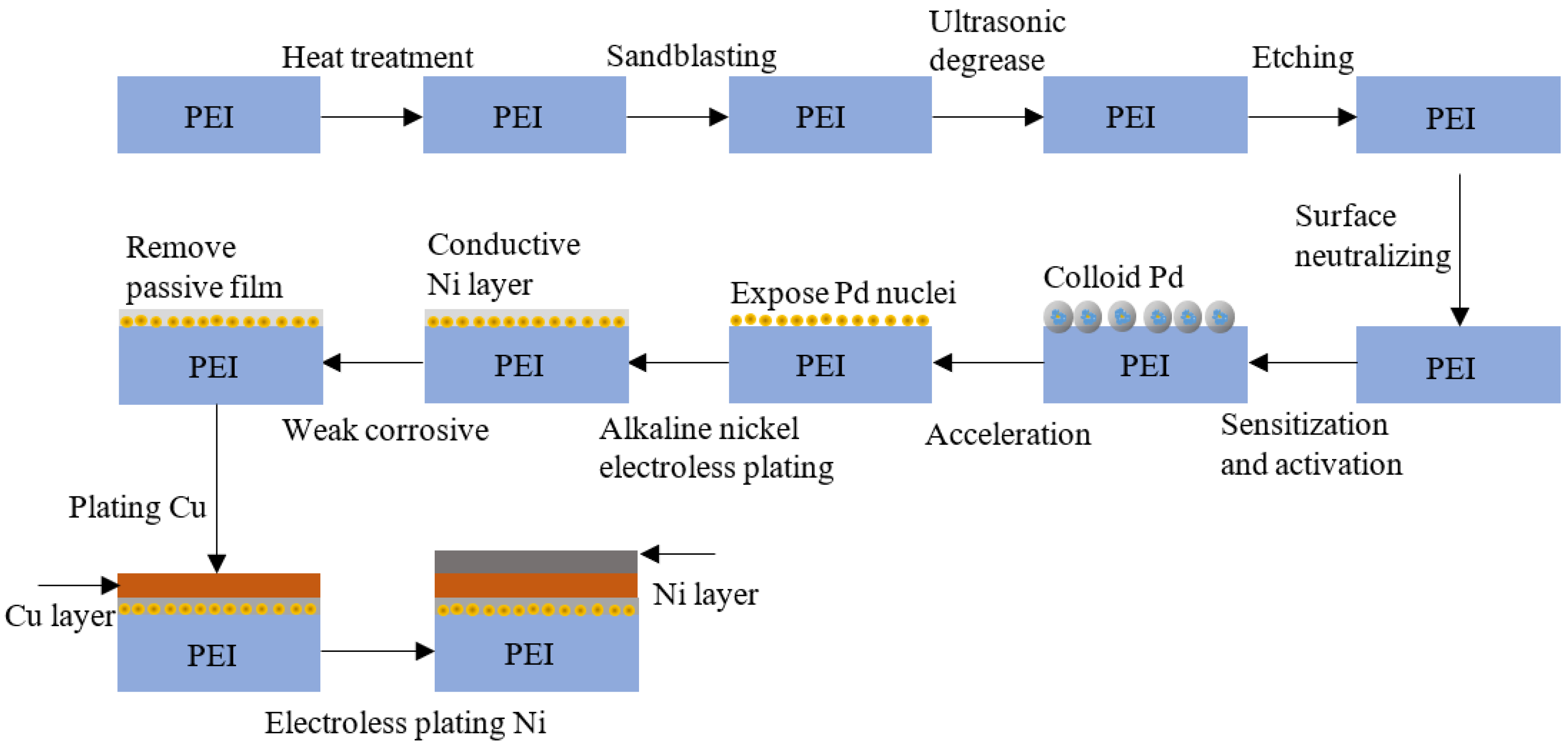
2.1. Pretreatment and Preparation

We manufactured the PEI composite substrates with short glass fibers by injection molding, which could be used as electronic products in the communication field. The two-dimensional drawings of the PEI composite substrate are displayed in Figure 1.
Figure 2 shows the process flowchart for surface metallization on PEI substrates. The preparation of metallization of the PEI substrate was performed in the subsequent steps: (1) heat treatment, (2) machine coarsening, (3) ultrasonic degrease, (4) chemical etching, (5) surface neutralizing, (6) sensitization and activation, (7) acceleration, (8) alkaline nickel electroless plating, (9) weak corrosion, (10) copper electroplating, and (11) acid electroless nickel plating. After each step, we washed and rinsed the substrates in deionized water. Table 1 displays each process involved in metallization on PEI substrates. The details for each step are as follows:
Heat treatment: We heat treated PEI substrates at 50~100 °C for 30 min, then 200 °C for 4~4.5 h.
Sandblasting: We sandblasted with 5 kg pressure for holding time of 4~5 s to roughen the PEI surface. These sands were composed of white Al2O3 grits with sizes ranging from 9.8 to 10.2 μm. The distance between the nozzle and the sample was about 80~90 cm. We immersed the sandblasted samples in deionized water, then took them out and placed them horizontally. The sandblasting resulted in an increase in the surface roughness, improving the adhesion between the layer and the substrate.
Ultrasonic degrease: After sandblasting, we degreased the PEI samples and cleansed in the ultrasonic cleaning machine with alkaline solution 5.0 M NaOH for ~20 min. Then, we rinsed in the deionized water.
Chemical etching: We chemically etched the samples in a mixture of chromium hexavalent, containing chromium trioxide of 200–400 g/L and 10 % sulfuric acid solution, and then we rinsed with water. We set the bath temperature in a range from 55 to 60 °C, and the etching time was 15–25 min.
Surface neutralizing: This step was to remove excess chromate from the surface and to neutralize the substrate because of the residual Cr6+ on the sample after chemical etching. We performed this step to avoid affecting the other solution, and to neutralize and adjust the samples according to Table 1. This mixed solution could modify the surface of the PEI substrate after etching, and might supply a positively charged group, which could be helpful to absorb the negatively charged Pd group. For some special polymer composite materials, such as PEI and PI composite polymer materials, this step has to be performed after the etching process to obtain much more Pd species for the next step-activation/sensitization process. However, for the metallization of ABS polymer materials, this step is not performed after the etching process (skip to the activation/sensitization process).
Sensitization and activation: We immersed the PEI substrates in the sensitization and activation solutions containing colloid palladium. The gray black Pd nanoparticles were formed by the redox reaction between palladium chloride (PdCl2) and stannous chloride (SnCl2) in the solution [37]. In this case, the Pd nuclei and nanoparticles surrounded by adsorbed Sn2+ species were formed on the surface of PEI substrates. The mechanism of colloidal Pd formation is based on the SnCl2·2H2O solution, and Sn2+ ions in the solution can reduce Pd2+ ions to Pd atoms. The equations describing the reaction mechanism are as follows [38]:
SnCl2 + PdCl2 SnCl4 + Pd
Pd2+ + Sn2+ + 4Cl Sn(PdCl4)
Acceleration: Pd nuclei and nanoparticles were surrounded by adsorbed Sn2+ species, which could remove colloid to expose the surrounded Pd nuclei on PEI substrates under stirring and air-blowing conditions. It is a strong acid solution with a low pH value. The standard treatment time was 4 min at a temperature of 40 °C as the activated samples were immersed in the acceleration solution.
Alkaline electroless nickel plating: We used an alkaline chemical nickel plating to generate a conductive film at room temperature. When the activated samples were immersed in the solution, the reduction of Ni2+ ions occurred, and an initial nickel layer was formed on the PEI substrates. During deposition, after a few minutes, the surface of the substrate slowly became shiny in the solution, inferring that the deposition of the metallic layer occurred. Subsequently, we observed that the reaction intensified on the surface of the samples because lots of small bubbles were released from the bath, and the Ni autocatalysis resulted in a vigorous reaction in the solution. Lastly, the Ni layer was deposited on surface of the PEI substrates. The surface of the samples presented a metallic appearance. The bath chemistry and deposition parameters are listed in Table 2. We controlled the thickness of the layer by the deposition time. The thickness of the initial electroless Ni layer was about 2 µm.
Weak corrosion: Weak corrosion is one of the key processes before the electrodeposition of copper layer. This is a surface activation process. This step is to remove the passivation film formed on the surface of the initial nickel layer, ensuring that good adhesion between the nickel layer and the copper coating. The weak corrosive solution was composed of an aqueous solution with 10% hydrochloric acid, immersed at room temperature for 30 s.
Cu electroplating: The electrodeposition conditions and bath chemistry for Cu electroplating are displayed in Table 2. We electrodeposited the thick Cu coating on the initial Ni layer in an alkaline solution at room temperature for 25 min (a good electrical conductive layer). The thickness of the Cu interlayer was about 20 µm. We controlled the thickness of the Cu coating by the deposition potential and time. We used two Cu plates as the anode, and used the samples with an initial Ni layer as cathodes. During electroplating, the solution was stirred by continuous bubbles, and the distance of the anode and cathode was about 25 cm.
Acid electroless Ni top layer: We deposited the top-layer Ni, as an anti-corrosive layer, on the surface of Cu/Ni PEI composite by electroless process in acidic solution for 20 min. The deposition conditions and bath chemistry are displayed in Table 2. The thickness of the top-surface Ni layer was about 6 µm.

2.2. Adhesion Force Test

We made sets of 4 × 4 cross-hatched scratches, with an interscratch distance of 1 mm and cross scratches at ~90°, on the deposits after drying. We applied a 3 M tape (610-1PK special test tape produced by 3M Company) over the grid, placing the center of the tape over the grid, and smoothed into place with a finger. After holding on 90 s, we removed the tape by seizing the free end and pulled it off rapidly at 90°. We assessed the adhesion force between the layer and the substrate according to the cross-cut testing standard of ASTM-D3359-09 (see Table 3). We repeated the cross-cut tests at least twice to evaluate the adhesion force between the substrate and the layer.

2.3. Characterizations

We evaluated the average surface roughness values of the PEI substrates before and after sandblasting by a surface profilometer (BRUKER ContourGT K0) with a 12.5 µm radius tip.
We recorded contact angles of the PEI substrates before and after sandblasting using a goniometer (FM4000, KRUSS Germany). The liquid we used was distilled water, 5 μL in volume, which we dropped on the surface of the samples in order to measure the contact angle. We determined the final contact angle three times at different places on the surface of the samples, using the well-known Young’s Equation (3) for describing the contact angle θ on a solid surface,
c o s θ = ( γ S V γ S L ) γ L V
where γSV, γSL, and γLV are the interfacial free energy per unit area of the solid–vapor, solid–liquid, and liquid–vapor interfaces, respectively. A simple model to characterize the influence of the surface roughness on the wettability of a solid was proposed by Wenzel Equation (4), which can be represented as follows:
c o s θ * = R ( γ S V γ S L ) / γ L V = R c o s θ
where R is the solid surface roughness, defined as the ratio between the actual surface area of a rough surface to the projected area. The above equation shows the relationship between the contact angle of the flat surface θ and that of the fractal surface θ *. We determined the surface energy by contact angle measurements using the Young–Dupre Equation (5).
γ = γ w 4 ( 1 + c o s θ ) 2
where γ is the surface energy of the solid, γ w = 73 mJ/m2 is the surface energy of the liquid water, and θ is the measured contact angle.
We observed the microstructure and morphology of the surface and cross-section of the deposits by a scanning electron microscopy (SEM, Zeiss-Supra55). We set the scanning rate to 40 s at an operating voltage of 10 kV. We determined the chemical composition of the deposit by X-ray energy-dispersive spectroscopy (EDS, X-act) detector. We measured the chemical state of ions in the solution using a UV Spectrophotometer (UV-3600 Japan).
We performed X-ray photoelectron spectroscopy (XPS) measurements in ultrahigh vacuum (3.3 × 10⁻⁸ Pa base pressure) using a 5700 ESCA System (PHI, NY, USA). We irradiated the samples with an Al-Kα monochromatic source (1486.6 eV) and analyzed the outcome electrons by a spherical capacitor analyzer using slit aperture of 0.8 mm. We analyzed the samples at the top-surface. We used the carbon signal for C–1s at 285 eV as an energy reference for the measured peaks. In order to identify the elements on the surface of the film, we performed a low-resolution survey spectrum over a wide energy range (0–1000 eV). We acquired high-resolution spectra with a pass energy of 23.5 eV at increments of 0.1 eV·step−1, to allow precise determination of the position of the peaks and their shape. We performed curve-fitting with Gaussian–Lorentzian function, using the XPSPEAK software. We fixed two fitting parameters—the position of the peak and its full width at half-maximum (FWHM)—within ±0.2 eV.

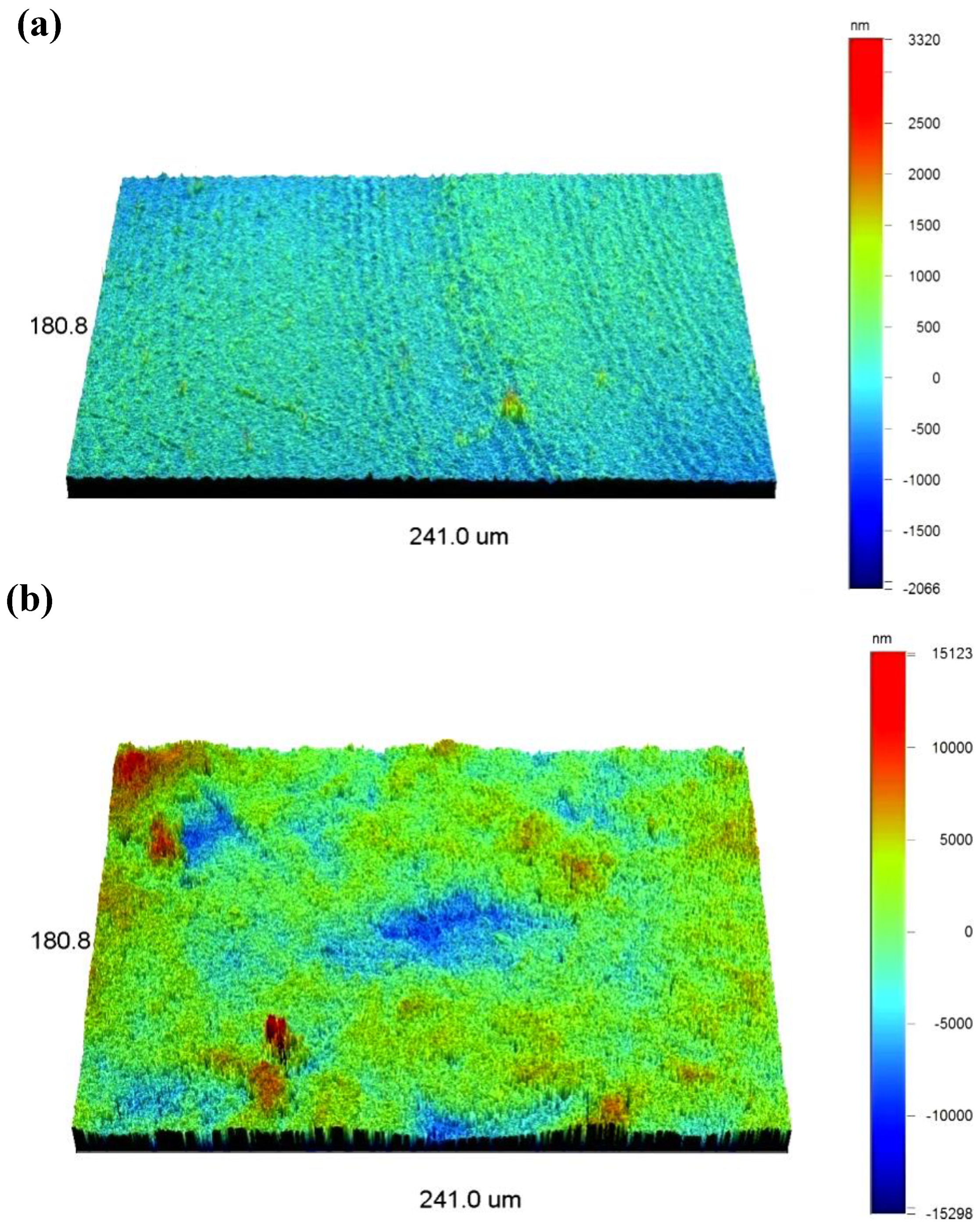
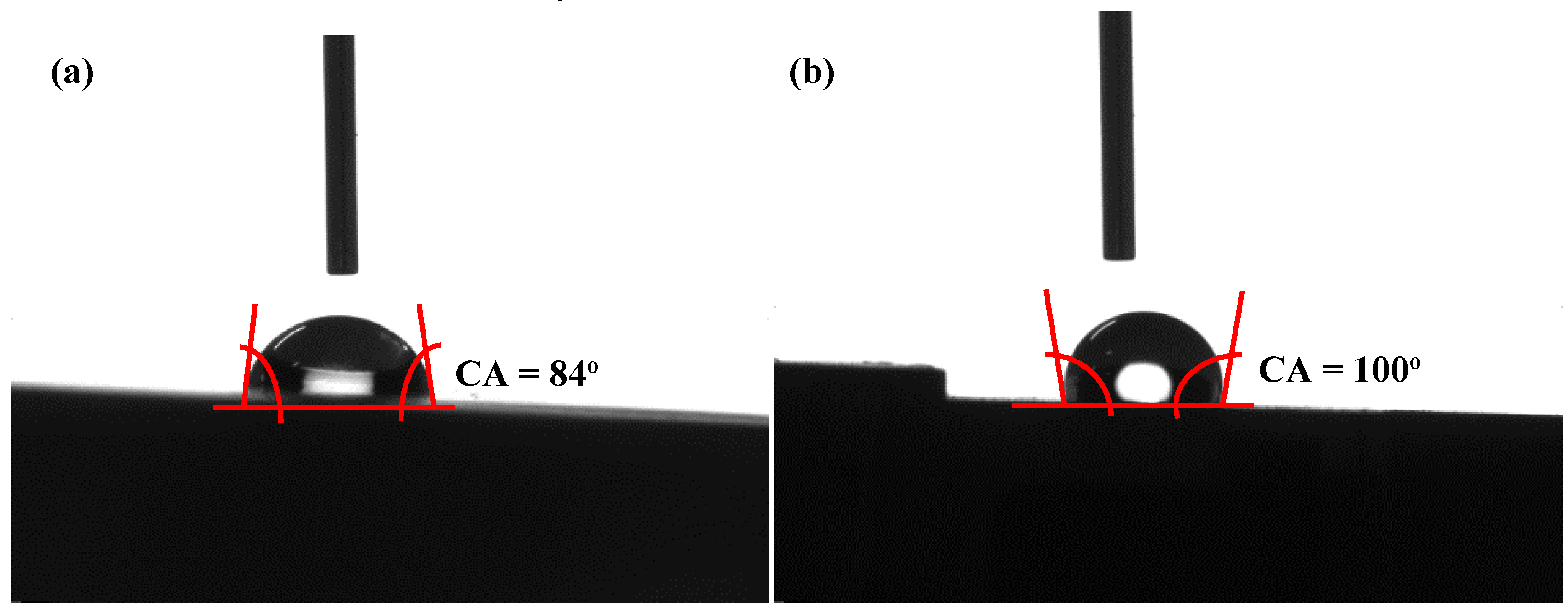
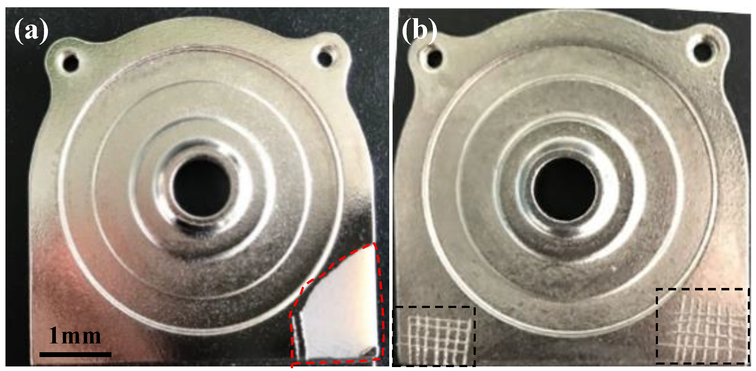
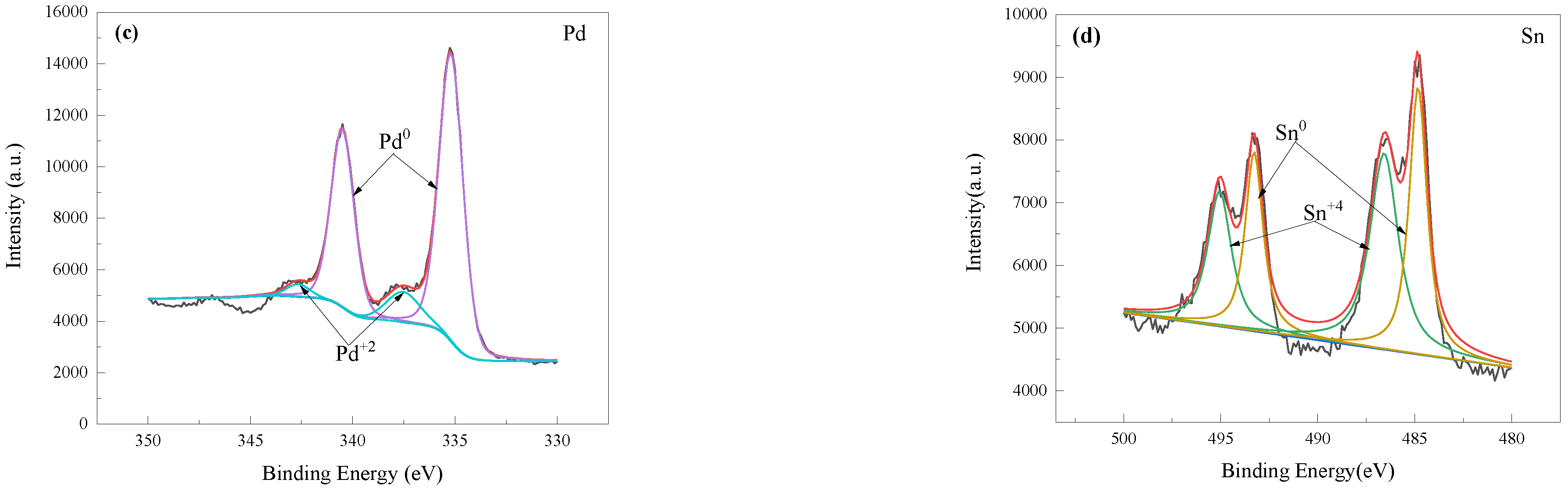
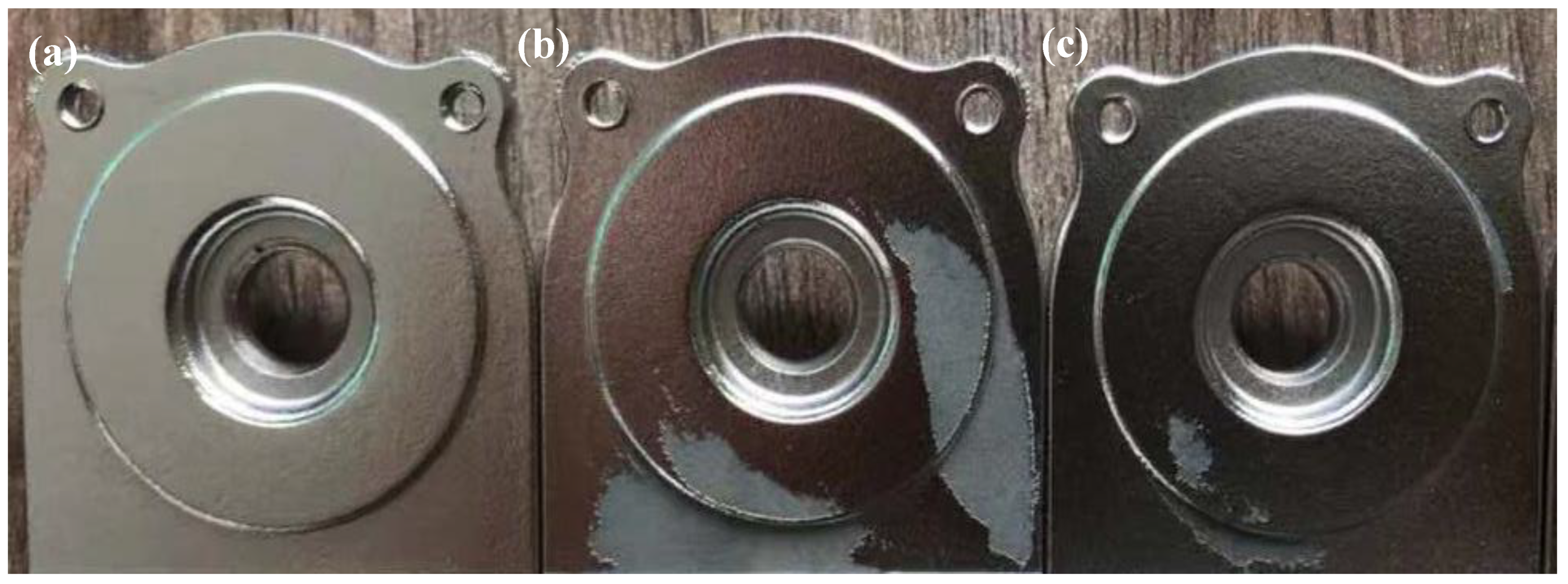
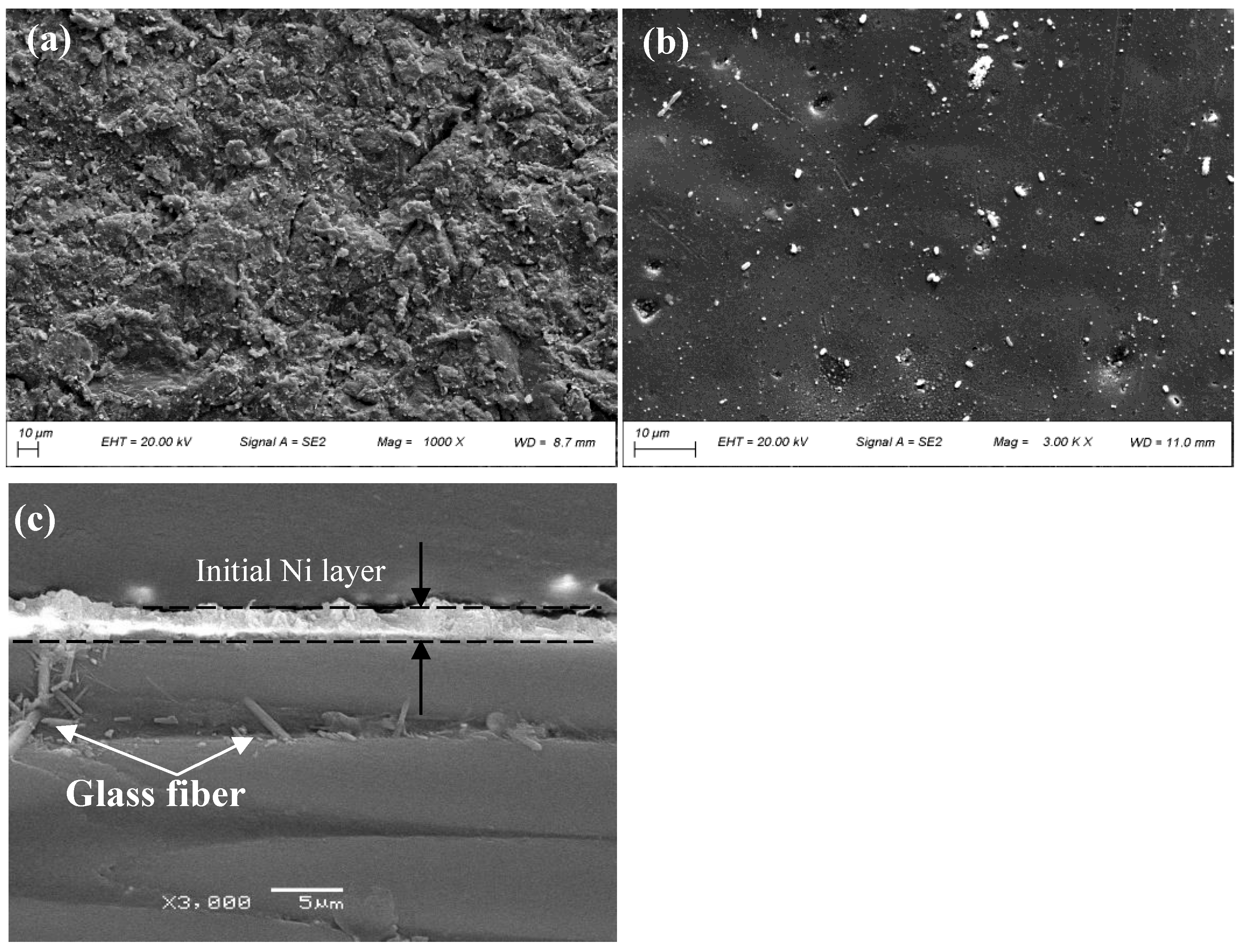
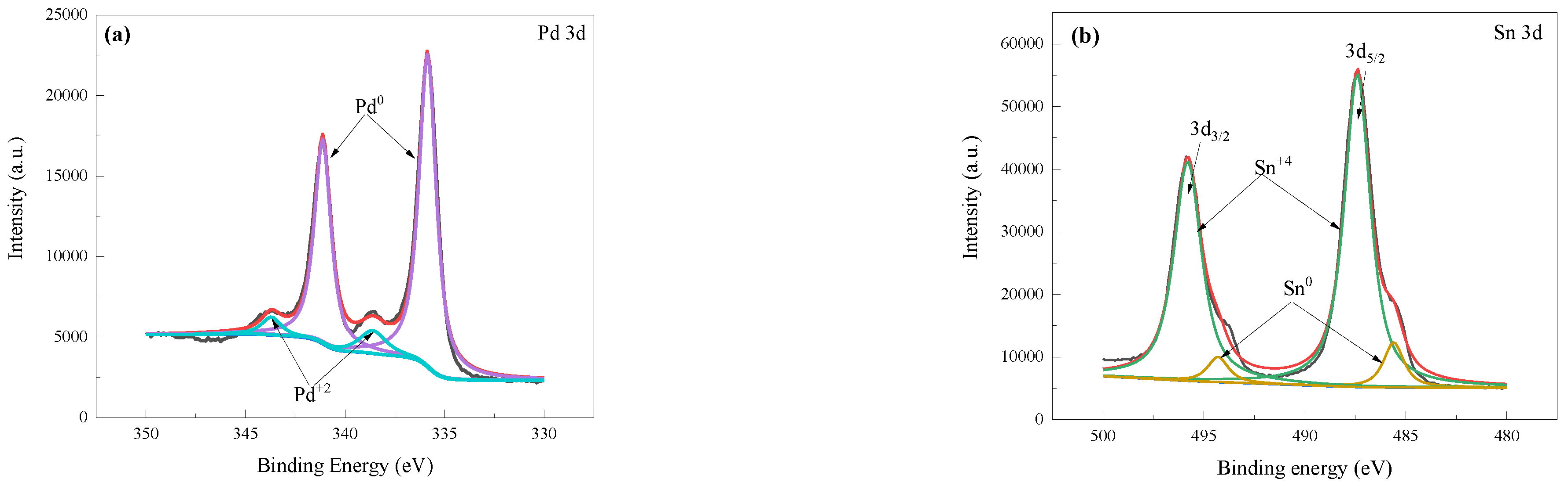
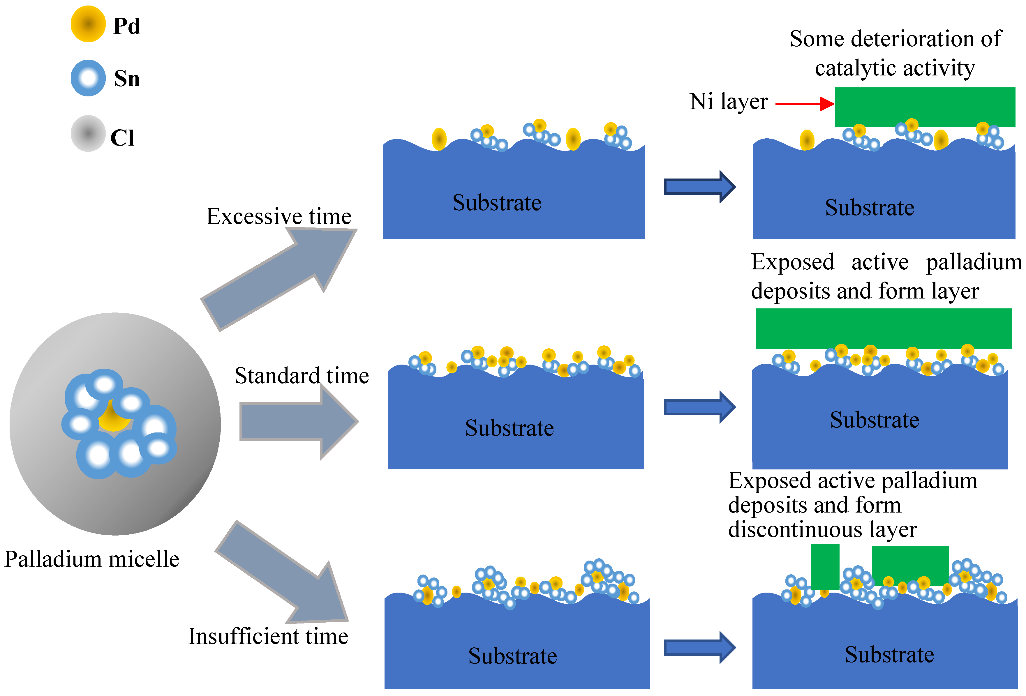
3. Results and Discussion

Figure 3 displays the 3D images of the surface morphology of the PEI substrate before and after the sandblasting process. The average surface roughness (Ra) values of the surface of the PEI substrate before and after sandblasting were 117 nm and 2125 nm, respectively. The surface roughness increased significantly after the sandblasting process. The surface of the PEI substrate was smooth (Figure 3a); however, the surface of the PEI substrate after sandblasting looked like a “mountain chain” (Figure 3b), indicating the surface became rough, which could contribute to improving the adhesion of the layer and the PEI substrate.
The effect of sandblasting on the wettability of the PEI substrate is observed in Figure 4. The surface of the PEI substrate before sandblasting shows a high wettability at a contact angle of about 84° (Figure 4a). After sandblasting, the contact angle increased to 100° (Figure 4b), indicating a low wettability. The specific surface area significantly increased after sandblasting process. The calculated surface energies of the PEI substrates before and after sandblasting were equal to 34.3 mJ/m2 and 60 mJ/m2, respectively. This indicated that the specific surface area significantly increased after the sandblasting process. The Wenzel and Cassie models contributed to the effect of surface roughness on wettability. The Wenzel model shows that a rough material surface has a higher surface area than a smooth one, which increases its hydrophobicity. The Cassie model shows that air trapped on the rough surface enhances the hydrophobicity because the drop is partially sitting on air. According to Equations (4) and (5), the ratio R is greater than unity, thus the wettability increases ( θ * <   θ ) for a hydrophilic situation, and decreases ( θ * > θ ) for a hydrophobic one. Therefore, this result agrees with the Wenzel equation. However, the surface wettability of the PEI substrate after sandblasting pretreatment can be improved to some degree after the chemical etching process. A good surface wettability of the PEI substrate can enhance the absorption of the activated Pd species in an activation solution. Therefore, more activated Pd particles were fixed and attached at the top-wetted surface, resulting in the increase of surface reactive sites. It can be inferred that the adhesion of the Ni layer was enhanced by the increase of the surface reactive sites.
The adhesion between the Ni/Cu/Ni multilayer and the polymer substrate was influenced by the sandblasting process. Figure 5 shows the digital images of the Ni/Cu/Ni deposits on PEI substrates with and without sandblasting. After the deposition of three layers of Ni/Cu/Ni deposits on PEI substrates, the adhesion of the deposits on PEI substrates was assessed by the cross-cut test with a 3M tape. The Ni/Cu/Ni deposit on the PEI substrate appears silver colored. The surface of the deposit was uniform and dense, with no evidence of defects. The Ni/Cu/Ni multilayer exhibited a poor adhesion with PEI substrates after the cross-cut test (Figure 5a). The cross-scratched deposit was detached from the substrate after peeling the tape. The affected area was in the range of 90~99% of the lattice and the adhesion can be classified as 0B grade. There is no evidence of the Ni/Cu/Ni deposit being removed from the sandblasted PEI substrates after the 3M tape, as shown in Figure 5b. The region between the grids kept intact, exhibiting good adhesion, and were classified as 5B grade. The interfacial adhesion strength between the Ni/Cu/Ni multilayer and PEI composites was remarkably improved by the pretreatment, which was attributed to the mechanical interlocking effect at the interface between the multilayer and the PEI substrates with high surface roughness. However, the Ni/Cu/Ni multilayer on the neat surface of the PEI substrates without the sandblasting process exhibited poor adhesion, which might be attributed to low surface roughness and some contaminations on the surface, such as release agent residues, resulting in poor adhesion between the multilayer and PEI substrates.
Figure 6 shows the SEM images and EDS pattern of the surface and cross-section of the initial thin-layer Ni. The surface of the initial Ni layer was rough because of the sandblasted PEI substrate, and some fine microcracks were observed on the surface (Figure 6a). The initial Ni layer consisted of some small aggregates and large particles. The surface of the initial Ni layer on the untreated PEI substrate was smooth; however, a fine microcrack was observed (Figure 6b). The thickness of the initial electroless Ni layer was about 2 µm. The interface between the layer and the substrate was obvious, with no evidence of delamination (Figure 6c). The P content in the initial Ni layer was 5.9 wt%. Generally, electroless Ni–P deposits with less than 5 wt% P have a crystalline structure with an average grain size of approximately 2–15 nm, and the films with more than approximately 10 wt% P show an amorphous phase compared with Ni. Within the intermediate concentration range, nanocrystallite was embedded in an amorphous matrix [18]. Therefore, in this work, this initial Ni layer on the PEI substrate was composed of a mixture of amorphous and nanocrystalline phases.
Figure 7 shows the microstructure and morphology of the surface and fracture of the Ni/Cu/Ni multilayer on the sandblasted PEI substrate. The visual appearance was a continuous and homogeneous layer with a low presence of visible defects (Figure 7a). There is a continuous film. The globular shape of the top of the columnar features can be observed. However, the top-surface of the Ni layer was also composed of some small aggregates with sizes of 2.0~8.0 μm. The surface was relatively rough due to the rough surface of the PEI substrate. The fracture of the multilayer on the PEI composite is displayed in Figure 7b, which was treated by a mechanical cutting machine. The thickness of the top-surface Ni layer was about 6.31 µm. The thickness of the Cu interlayer was about 20 µm. Glass fibers and some holes were observed on the fracture of the PEI substrate. After the sandblasting process, the surface generates a non-uniform surface structure characterized by dimples and furrows. There were no noticeable cracks, and this behavior demonstrated a high-quality composite multilayer. There is no evidence of the delamination between the layers and the deposit and the substrate.
Generally, colloid palladium was used as a kind of catalyst for the surface metallization of the polymer substrates [39]. The catalytic activity of colloid palladium not only played an important role in the appearance quality of the surface metal layers but also affected the industrialization applications of metallic layers on polymer substrates. The excess SnCl2·2H2O surrounds palladium to form colloidal palladium. The activation process can be realized by one or two steps. The latter includes the sensitization of a SnCl2 acidic solution and the activation of a PdCl2 acidic solution. Firstly, the substrate was immersed into a solution in order to adsorb Sn cations at the surface of the PEI substrates. Secondly, a batch of samples were immersed in the activation solution containing the catalytic chemical, resulting in the formation of the catalyst species. However, the colloidal palladium solution just needs one step in this work. A commercial solution with a combination of sensitizer and activator contains a palladium complex. The Pd complex activation solution is gray black due to the formation of the (PdSn6)Cl14 complex by the following reaction (6):
6SnCl2 (excess) + PdCl2 = (PdSn6)Cl14
The colloidal palladium solution will fail. After a period in the beaker, the color of the solution will be changed to yellow. There is no deposit formed in the solution. Figure 8 shows the UV–vis spectra and macrograph of the activation solution in the glass bottles. It can be observed that the colloidal palladium solution shows the gray dark color; however, the color of the colloidal palladium solution became yellow after a period (about 10 days exposed to air). According to the observation of the UV–vis spectra, the chemical state of the ions in the solution was changed after 10 days exposed to air. This is possible due to the oxidization of Sn2+ ions, as in the following reaction (7):
2SnCl2+ O2 + 4HCl = 2SnCl4 + 2H2O
After the PEI substrates were treated and activated by the sensitization/activation process, the substrates were thoroughly rinsed into acceleration solution at the temperature of 70 °C to remove excess hydroxides, oxides, and salts of tin, leaving active catalyst species, such as metallic Pd and PdSnx nanoparticles [34]. This step is commonly known as acceleration. The accelerator is a strong acid or alkaline solution, which plays an important role in energizing the mixed catalysts. The electroless plating of an initial Ni layer will not occur without the acceleration process. The action and function of the accelerator is to convert hydrolyzed stannous and PdCl2 to active metallic Pd. The surface catalytic activity of the substrate is related to the number of catalytic nuclei of Pd, which depends on the degree of acceleration and the amount of SnC12/PdC12 adsorbed on the surface of PET substrates.
Figure 9 shows the XPS spectra of the top-surface of the sample after the sensitization/activation and acceleration processes. The surface of the PEI substrates treated only with the sensitization/activation solution shows Sn, O, Pd, and C signal peaks. The observed carbon signal was not characteristic of the PEI and is attributed to normal environmental contamination. It can be observed that Sn 4d (26.25 eV), Sn3d (487.76 eV), and Sn 3p (716.4 eV) signals were eliminated and weak after the acceleration process but the Pd and Cl signals were still strong. Therefore, the acceleration process could be helpful to convert hydrolyzed stannous and PdCl2 to active metallic Pd. The Sn2+ and Sn4+ ions were easily removed from the colloid solution.
Figure 10 shows the high-resolution XPS spectra of the Pd and Sn. The Sn(IV) signal can be observed before acceleration. Before acceleration process, the Pd0 and a small amount of Pd2+ were present, at the same time there are main Sn4+ ions at 486.3 eV for several stannous or stannic oxides or hydroxides, and small amounts of Sn0 at 485.5 eV in the solution. After the acceleration process, both Sn and Sn(IV) species were present, and colloidal Pd was mainly present in Pd0 metallic state. It can be indicated that the primary Pd species on the surface of the PEI substrate are in the metallic state before and after acceleration, although a fraction of the Pd is oxidized during the sensitization/activation and acceleration processes, which could be attributed to the sensitization/activation solution being used for a period. After the acceleration process, the intensity of the Sn 3d5/2 signal peak decreases dramatically, and two nearly equal reflections were observed with binding energies of 485.2 eV and 486.8 eV (Figure 10d). The reflection at a relatively low binding energy is attributed to metallic Sn species, while the reflection at a high binding energy is due to the remaining stannic hydroxides. Thus, it is assumed that only the metallic Sn is associated with the active catalytic center. After the acceleration, lots of Sn species have been removed. The highly active catalyst of Pd0 induces Ni deposition instantaneously by immersion in an electroless plating Ni bath.
The initial nickel solution is an alkaline solution produced from electroless plating. This solution is strongly alkaline (pH > 12). This bath produces a binary nickel–phosphorous (Ni-P) alloy deposit. In an alkaline bath based on the dehydrogenation of the reducing agent, the deposition mechanism of the electroless Ni-P coating involved the following chemical reactions [16,18]:
H2PO2 + 2OHH + H2PO3 + H2O
Ni2+ + 2HNi0 + H2
H2PO2 + H2OH + P + 1/2H2
H2O + HOH + H2
According to Equations (9)–(11), the formation of hydrogen bubbles in the solution was from the hydride ions and water. After a standard acceleration time, the masking salt and the reactive Pd or metallic PdSnx were exposed, which then initiates the deposition of Ni, forming a conductive Ni layer for the next step of electroplating. The complete Ni layer was deposited on the PEI substrate, as displayed in Figure 11a. However, the acceleration time will affect the deposition of Ni for electroless plating (see Figure 11b,c). In the case of insufficient acceleration time, the colloid reacts with the strong acid insufficiently, resulting in incomplete exposure of the active Pd. Therefore, only exposed active Pd0 atoms or metallic PdSnx alloys can induce the reduction of Ni2+ ions and the formation of the initial Ni layer. However, under excessively accelerated conditions, prolonged exposure to acidic media may cause the entire colloidal shell (including the portion locked to the substrate surface) to react, followed by the leaching of the Pd core, resulting in a loss of catalytic activity; furthermore, excessively prolonged acceleration treatment reduces catalytic activity. During the long acceleration step, a part of Pd may be oxidized [36]. At the same time, stirring the solution and air may dislodge the Pd nuclei from the substrate surface. Therefore, the appearance quality of the Ni deposit on the PEI substrate was poor, showing a skip plating defect.
As displayed in Figure 12, colloid Pd mainly comprised Pd as the activation core and Sn and Cl as a protective shell core [38]. Firstly, the colloidal nucleus selectively adsorbed the Sn2+ and Sn4+ ions in the solution to form a dense layer. The colloidal Pd-Sn nanoparticles were formed with a Pd nucleus as the core, and Snn+ as the shell core. Then, the colloidal Pd-Sn nanoparticles with a positive charge would absorb the Cl ions with a negative charge for neutralization. A ring of encirclement was generated around the colloidal Pd-Sn nanoparticles in order to protect the Pd core. Therefore, the electrically neutral colloid Pd was obtained in the form of PdxSnyClz or {Pdm·2Snn+·2(n − x)Cl}·2xCl complexes [40]. After acceleration, the chemical nature of the adsorbed species was also addressed in previous research [29,31]. Cohen and Meek [41] discovered that Sn4+ in the form of stannic hydroxide was found before the acceleration process, and that both Sn(OH)4 and Pd-Sn alloys were present after acceleration. Osaka et al. [42] examined catalyzed surfaces and reported that a Pd–Sn alloy was formed with the removal of Sn4+ ions during acceleration. Burrell et al. [36] reported that only Sn4+ was found before acceleration, and both metallic Sn and Sn4+ were present after acceleration; furthermore, he found that metallic Pd0 was primarily present before and after the acceleration process. Pd2+ species from a PdCl2 solution were attached on the PEI surface and, subsequently, Pd2+ species were reduced into Pd0. The Pd0 catalyst allowed an instantaneous initiation of the Ni deposit by immersion in a plating bath. After the standard acceleration time, the masking salts are leached away and exposed the active Pd or the metallic PdSnx, which is then able to initiate the deposition of the Ni layer, forming a conductive layer. However, if the acceleration time after the sensitization/activation process is too long or short, it could influence the deposition of the electroless Ni layer. In insufficient acceleration conditions, the colloid does not fully react with the strong acid and results in an incomplete exposure of the active Pd nanoparticles. Therefore, only the exposed active Pd atom or the metallic PdSnx alloy nanoparticles can induce the reduction of Ni2+ ions and form the initial Ni layer. However, in the excessive acceleration condition, prolonged exposure to the acid media may lead to the colloid shells reaction, which then leach out of the Pd nuclei, resulting in some deterioration of catalytic activity through prolonged treatment [43]. During acceleration, a fraction of the Pd nanoparticles might be oxidized after a period of time [36]. At the same time, the Pd0 nuclei might be detached from the substrate surface by stirring the solution and air-blowing in the electrolyte. The excessive acceleration condition could result in the non-uniform and discontinuous layer deposited on the surface of the PEI substrates.

4. Conclusions

Ni/Cu/Ni multilayer metallization on PEI resin reinforced with glass fibers was successfully made by a two-step metallization process, including sandblasting and activation/acceleration. However, the pretreatment processes have an influence on the appearance quality and adhesion of the Ni/Cu/Ni multilayer deposits on the PEI substrates. The surface roughening process, namely sandblasting, influenced the adhesion and appearance quality of the deposits on the PEI substrates. The average surface roughness of the substrates with and without the sandblasting process were 117 nm and 2125 nm, respectively. The surface roughness of the PEI substrate significantly increased after sandblasting, which could improve the adhesion of the metallic multilayer. The pretreatment processes of sensitization/activation and acceleration affected the appearance quality of the deposit on the PEI substrate. After the sensitization/activation process, Pd0 and a small amount of Pd2+ were present, and there were lots of Sn4+ ions for a few stannous or stannic oxides or hydroxides. However, the metallic state was the primary Pd species on the substrate after acceleration. The acceleration had an effect on the deposition of Ni for electroless plating. After the standard acceleration time, the initial electroless continuous Ni layer was formed on the surface of the PEI substrates as a conductive layer for the next step of the electroplating process.

Author Contributions

W.W. planned, wrote, and supervised this work; X.X. and D.X. prepared the multilayer films and co-wrote and edited this paper; W.W. supervised Masters student D.X.; X.X., D.X., J.H. and G.H. performed some experiments and tests; Y.Z., W.W. and P.J. performed and analyzed characterization of materials and samples; K.L. and L.T. conceived the rest of the experiments and provided experimental platform and three months of internship experience for Masters students. All authors have read and agreed to the published version of the manuscript.

Funding

This research was funded by Jiaqi Huang acknowledges funding from the Postgraduate Research & Practice Innovation Program of Jiangsu Province (Grant no. SJCX22_1429).

Institutional Review Board Statement

Not applicable.

Informed Consent Statement

Not applicable.

Data Availability Statement

Not applicable.

Acknowledgments

The authors thank Ying Wang and Jun Jiang from the Analysis and Testing Center of Changzhou University for discussion and helping in the surface roughness and XPS measurement, respectively.

Conflicts of Interest

The authors declare no conflict of interest.

References

  1. Viscusi, A.; Durante, M.; Astarita, A.; Boccarusso, L.; Carrino, L.; Perna, A.S. Experimental Evaluation of Metallic Coating on Polymer by Cold Spray. Procedia Manuf. 2020, 47, 761–765. [Google Scholar] [CrossRef]
  2. Esfahani, R.N.; Shuttleworth, M.P.; Doychinov, V.; Wilkinson, N.J.; Hinton, J.; Jones, T.D.A.; Ryspayeva, A.; Robertson, I.D.; Marques-Hueso, J.; Desmulliez, M.P.Y.; et al. Light based synthesis of metallic nanoparticles on surface-modified 3D printed substrates for high performance electronic systems. Addit. Manufact. 2020, 34, 101367. [Google Scholar] [CrossRef]
  3. Ding, S.; Zou, B.; Wang, P.; Ding, H. Effects of nozzle temperature and building orientation on mechanical properties and microstructure of PEEK and PEI printed by 3D-FDM. Polym. Test. 2019, 78, 105948. [Google Scholar] [CrossRef]
  4. Polyakov, I.V.; Vaganov, G.V.; Yudin, V.E.; Smirnova, N.V.; Ivan’kova, E.M.; Popova, E.N. Study of polyetherimide and its nanocomposite 3D printed samples for biomedical application. Polym. Sci. Ser. A 2020, 62, 337–342. [Google Scholar] [CrossRef]
  5. Melentiev, R.; Yu, N.; Lubineau, G. Polymer metallization via cold spray additive manufacturing: A review of process control, coating qualities, and prospective applications. Addit. Manuf. 2021, 48, 102459. [Google Scholar] [CrossRef]
  6. Kouicem, M.M.; Tomasella, E.; Bousquet, A.; Batisse, N.; Monier, G.; Robert-Goumet, C.; Dubost, L. An investigation of adhesion mechanisms between plasma-treated PMMA support and aluminum thin films deposited by PVD. Appl. Surf. Sci 2021, 564, 150322. [Google Scholar] [CrossRef]
  7. Ferreira, A.A.; Silva, F.J.G.; Pinto, A.G.; Sousa, V.F.C. Characterization of Thin Chromium Coatings Produced by PVD Sputtering for Optical Applications. Coatings 2021, 11, 215. [Google Scholar] [CrossRef]
  8. Duguet, T.; Senocq, F.; Laffont, L.; Vahlas, C. Metallization of polymer composites by metalorganic chemical vapor deposition of Cu: Surface functionalization driven films characteristics. Surf. Coat. Technol. 2013, 230, 254–259. [Google Scholar] [CrossRef]
  9. Addou, F.; Duguet, T.; Ledru, Y.; Mesnier, D.; Vahlas, C. Engineering Copper Adhesion on Poly-Epoxy Surfaces Allows One-Pot Metallization of Polymer Composite Telecommunication Waveguides. Coatings 2021, 11, 50. [Google Scholar] [CrossRef]
  10. Gonzalez, R.; Ashrafizadeh, H.; Lopera, A.; Mertiny, P.; McDonald, A. A Review of Thermal Spray Metallization of Polymer-Based Structures. J. Therm. Spray Technol. 2016, 25, 897–919. [Google Scholar] [CrossRef]
  11. Parmar, H.; Tucci, F.; Carlone, P.; Sudarshan, T.S. Metallisation of polymers and polymer matrix composites by cold spray: State of the art and research perspectives. Int. Mater. Rev. 2021, 67, 385–409. [Google Scholar] [CrossRef]
  12. Shacham-Diamand, Y.; Osaka, T.; Okinaka, Y.; Sugiyama, A.; Dubin, V. 30 years of electroless plating for semiconductor and polymer micro-systems. Microelectron. Eng. 2015, 132, 35–45. [Google Scholar] [CrossRef]
  13. Ghosh, S. Electroless copper deposition: A critical review. Thin Solid Films 2019, 669, 641–658. [Google Scholar] [CrossRef]
  14. Huang, J.; Gui, C.; Ma, H.; Li, P.; Wu, W.; Chen, Z. Surface metallization of PET sheet: Fabrication of Pd nanoparticle/polymer brush to catalyze electroless nickel plating. Compos. Sci. Technol. 2021, 202, 108547. [Google Scholar] [CrossRef]
  15. Dupenne, D.; Lonjon, A.; Dantras, E.; Pierré, T.; Lubineau, M.; Lacabanne, C. Carbon fiber reinforced polymer metallization via a conductive silver nanowires polyurethane coating for electromagnetic shielding. J. Appl. Polym. Sci. 2020, 138, 50146. [Google Scholar] [CrossRef]
  16. Wu, W.P.; Liu, J.W.; Miao, N.M.; Jiang, J.J.; Zhang, Y.; Zhang, L.; Yuan, N.Y.; Wang, Q.Q.; Tang, L.X. Influence of thiourea on electroless Ni-P films on silicon substrates. J. Mater. Sci. Mater. Electron. 2019, 30, 7717–7724. [Google Scholar] [CrossRef]
  17. Wu, W.; Wang, X.; Xie, D.; Zhang, Y.; Liu, J. Corrosion failure analysis of Ni-P film of aircraft fire detector components. Eng. Fail. Anal. 2020, 111, 104497. [Google Scholar] [CrossRef]
  18. Wu, W.-P.; Jiang, J.-J. Effect of plating temperature on electroless amorphous Ni–P film on Si wafers in an alkaline bath solution. Appl. Nanosci. 2017, 7, 325–333. [Google Scholar] [CrossRef]
  19. Dixit, N.K.; Srivastava, R.; Narain, R. Improving surface roughness of the 3D printed part using electroless plating. Proc. Inst. Mech. Eng. Part L J. Mater. Des. Appl. 2019, 233, 942–944. [Google Scholar] [CrossRef]
  20. Huang, J.; Wu, W.; Zhang, R.; Lu, G.; Chen, B.; Chen, Z.; Gui, C. Novel electrode material using electroless nickel plating for triboelectric nanogenerator: Study of the relationship between electrostatic-charge density and strain in dielectric material. Nano Energy 2022, 92, 106734. [Google Scholar] [CrossRef]
  21. Marques-Hueso, J.; Jones, T.D.A.; Watson, D.E.; Ryspayeva, A.; Esfahani, M.N.; Shuttleworth, M.P.; Harris, R.A.; Kay, R.W.; Desmulliez, M.P.Y. A rapid photopatterning method for selective plating of 2D and 3D microcircuitry on polyetherimide. Adv. Funct. Mater. 2018, 28, 1704451–1704459. [Google Scholar] [CrossRef]
  22. Marline, C.; Maurice, R.; Yves, G. Direct Ni electroless metallization of poly(etherimide) without using palladium as a catalyst. Trans. Mater. Heat Treat. Proc. 14th IFHTSE Congr. 2004, 25, 1106–1111. [Google Scholar]
  23. Jones, T.D.A.; Ryspayeva, A.; Esfahani, M.N.; Shuttleworth, M.P.; Harris, R.A.; Kay, R.W.; Desmulliez, M.P.Y.; Marques-Hueso, J. Direct metallisation of polyetherimide substrates by activation with different metals. Surf. Coat. Technol. 2019, 360, 285–286. [Google Scholar] [CrossRef]
  24. Alodan, M.A. Metallizing Polyetherimide Resin Reinforced with Glass Fibers. J. King Saud Univ. Eng. Sci. 2005, 17, 251–259. [Google Scholar] [CrossRef]
  25. Zhang, F.-T.; Xu, L.; Chen, J.-H.; Zhao, B.; Fu, X.-Z.; Sun, R.; Chen, Q.; Wong, C.-P. Electroless Deposition Metals on Poly(dimethylsiloxane) with Strong Adhesion as Flexible and Stretchable Conductive Materials. ACS Appl. Mater. Interfaces 2018, 10, 2075–2082. [Google Scholar] [CrossRef] [PubMed]
  26. Wu, W.; Xie, D.; Huang, J.; Wang, Q.; Chen, Q.; Huang, J. Adhesion enhancement for nickel layer deposited on carbon fiber reinforced polymer (CFRP) composites by pretreatment processes for lightning strike. J. Adhes. 2022, 1–24. [Google Scholar] [CrossRef]
  27. Fischer, A.J.; Meister, S.; Drummer, D. Effect of fillers on the metallization of laser-structured polymer parts. J. Polym. Eng. 2017, 37, 151–161. [Google Scholar] [CrossRef]
  28. Gebauer, J.; Burkhardt, M.; Franke, V.; Lasagni, A.F. On the Ablation Behavior of Carbon Fiber-Reinforced Plastics during Laser Surface Treatment Using Pulsed Lasers. Materials 2020, 13, 5682. [Google Scholar] [CrossRef]
  29. Li, J.F.; Lin, P.T.; Sun, H.R.; Li, X.X.; Sang, J.; Wang, X.G.; Li, Q.; Jin, Y.; Zhang, L.G. Selective metallization on CFRP composites by laser radiation and electroless plating. J. Phys. Conf. Ser. 2021, 2101, 012048. [Google Scholar] [CrossRef]
  30. Puliyalil, H.; Filipič, G.; Cvelbar, U. Chapter 9-Selective plasma etching of polymers and polymer matrix composites. In Non-Thermal Plasma Technology for Polymeric Materials-Applications in Composites, Nanostructured Materials and Biomedical Fields; Elsevier: Amsterdam, The Netherlands, 2019; pp. 241–259. [Google Scholar]
  31. Rao, C.H.; Kothuru, A.; Singh, A.P.; Varaprasad, B.K.S.V.L.; Goel, S. Plasma Treatment and Copper Metallization for Reliable Plated-Through-Holes in Microwave PCBs for Space Electronic Packaging. IEEE Trans. Compon. Packag. Manuf. Technol. 2020, 10, 1921–1928. [Google Scholar] [CrossRef]
  32. Xie, D.; Wu, W.; Huang, J.; Wang, X.; Zhang, Y.; Wang, Z.; Jiang, P.; Tang, L. Effect of electrodeposited Cu interlayer thickness on characterizations and adhesion force of Ni/Cu/Ni coatings on polyetherimide composite substrates. Int. J. Adhes. Adhes. 2021. Available online: https://www.researchgate.net/publication/355181252 (accessed on 8 July 2022).
  33. Ramaswamy, K.; O’Higgins, R.M.; Kadiyala, A.K.; McCarthy, M.A.; McCarthy, C.T. Evaluation of grit-blasting as a pre-treatment for carbon-fibre thermoplastic composite to aluminium bonded joints tested at static and dynamic loading rates. Compos. Part B Eng. 2020, 185, 107765. [Google Scholar] [CrossRef]
  34. Radoeva, M.; Monev, M.; Ivanov, I.; Georgiev, G.; Radoev, B. Adhesion improvement of electroless copper coatings by polymer additives. Colloids Surf. A Physicochem. Eng. Asp. 2014, 460, 441–447. [Google Scholar] [CrossRef]
  35. Guo, R.; Yin, G.; Sha, X.; Wei, L.; Zhao, Q. Effect of surface modification on the adhesion enhancement of electrolessly deposited Ag-PTFE antibacterial composite coatings to polymer substrates. Mater. Lett. 2015, 143, 256–260. [Google Scholar] [CrossRef]
  36. Burrell, M.C.; Smith, G.A.; Chera, J.J. Characterization of PdCl2/SnCl2 metallization catalysts on a polyetherimide surface by XPS and RBS. Surf. Interf. Analy 1988, 11, 160–164. [Google Scholar] [CrossRef]
  37. Touyeras, F.; Hihn, J.; Bourgoin, X.; Jacques, B.; Hallez, L.; Branger, V. Effects of ultrasonic irradiation on the properties of coatings obtained by electroless plating and electro plating. Ultrason. Sonochem. 2005, 12, 13–19. [Google Scholar] [CrossRef]
  38. Nicolas-Debarnot, D.; Pascu, M.; Vasile, C.; Poncin-Epaillard, F. Influence of the polymer pre-treatment before its electroless metallization. Surf. Coat. Technol. 2006, 200, 4257–4265. [Google Scholar] [CrossRef]
  39. Zhao, Y.; Zhan, L.; Tian, J.; Nie, S.; Ning, Z. Enhanced electrocatalytic oxidation of methanol on Pd/polypyrrole–graphene in alkaline medium. Electrochim. Acta 2011, 56, 1967–1972. [Google Scholar] [CrossRef]
  40. Shuai, H.; Jian, W.; Yu, H.L.; Tang, J.B.; Zhang, X. Microstructure characterization and formation mechanism of colloid palladium for activation treatment on the surface of PPTA fibers. Appl. Surf. Sci. 2020, 516, 146134. [Google Scholar]
  41. Cohen, R.; Meek, R. The chemistry of palladium—tin colloid sensitizing processes. J. Colloid Interface Sci. 1976, 55, 156–162. [Google Scholar] [CrossRef]
  42. Osaka, T. A Study on activation and acceleration by mixed PdCl2/SnCl2catalysts for electroless metal deposition. J. Electrochem. Soc. 1980, 127, 390–394. [Google Scholar] [CrossRef]
  43. Rantell, A.; Holtzman, A. The Role of Accelerators Prior to Electroless Plating of ABS Plastic. Trans. IMF 1974, 52, 31–38. [Google Scholar] [CrossRef]
Figure 1. Two-dimensional drawings of PEI composite substrate.
Metals 12 01359 g001
Figure 2. Process flowchart for metallization of PEI composite substrates.
Metals 12 01359 g002
Figure 3. 3D images of surface roughness for PEI composite before (a) and after (b) sandblasting process.
Metals 12 01359 g003
Figure 4. Water droplet contact angles on surface of PEI composite before (a) and after (b) sandblasting process.
Metals 12 01359 g004
Figure 5. Digital images of Ni/Cu/Ni multilayer deposits on PEI substrates without (a) and with (b) sandblasting process after cross-cut test by 3M tape.
Metals 12 01359 g005
Figure 6. SEM images of surface of alkaline electroless Ni layer on sandblasted PEI substrate (a) and on untreated PEI substrate (b); SEM image of cross-section of alkaline electroless Ni layer on untreated PEI substrate (c).
Metals 12 01359 g006
Figure 7. SEM images of top-surface (a) and fracture (b) of multilayer deposit on PEI substrate after sandblasting.
Metals 12 01359 g007
Figure 8. UV–vis spectra and macrograph of activation solution in the glass bottles.
Metals 12 01359 g008
Figure 9. XPS spectra of top-surface of the sample after sensitization/activation process (a) and after acceleration process (b).
Metals 12 01359 g009
Figure 10. High-resolution XPS spectra of Pd 3d and Sn 3d before and after acceleration process. XPS of Pd 3d (a) and Sn 3d (b) before acceleration process, and XPS of Pd 3d (c) and Sn 3d (d) after acceleration process.
Metals 12 01359 g010aMetals 12 01359 g010b
Figure 11. Digital macrographs of PEI samples: (a) standard condition (4 min), (b) short acceleration time (2 min), (c) excessive acceleration time (10 min).
Metals 12 01359 g011
Figure 12. Illustration of acceleration of Pd micelle and formation of initial Ni layer.
Metals 12 01359 g012
Table 1. Process conditions of surface neutralizing (Modifier A/B/C were purchased from MacDermid Co., Shanghai, China).
ItemCondition
Modifier A7–10%
Modifier B5–6%
Modifier C1.5–3%
Temperature (°C)50–60
Time (min)12–18
pH9–10
Note: Mixed solution is of deionized water.
Table 2. Process steps involved in metallization on PEI substrates.
Process StepProcess Condition
Heat treatmentFirst, T = 50~100 °C for 30 min, then 200 °C for 4~4.5 h.
Sandblasting5 kg pressure
Degreasing5 M NaOH at T = 25 °C for ~20 min under ultrasonic condition
Chemical etchingChromium trioxide of 200–400 g/L and 10% sulfuric acid, 55–60 °C, 15 min
Surface neutralizing5 M NaOH at T = 25 °C for ~20 min under ultrasonic condition
Sensitization and activation220–280 mL/L HCl; 3 g/L SnCl2·2 H2O; 2–4 mL/L Activator *; T = 25 °C; t = 10 min
Acceleration100 mL/L HCl, T = 40 °C, t = 2~10 min
Alkaline electroless Ni90–110 mL/L 160 A *; 25–35 mL/L 160 B *; 4–6 mL/L NH3·H2O; pH = 8.8–9.2; T = 25 °C and t = 8 min
Weak Corrosion10% HCl; t = 30 s
Cu electroplating55–60 g/L CuCO3; 30–40 g/L NaKC4H4O6·4H2O; 250–270 g/L C6H8O7;
10–15 g/L NaHCO3; pH = 8.5–9.5; T = 25 °C; Applied voltage = 2.5 V; t = 15 min
Acid electroless Ni15–25 g/L Ni(NH4)2(SO4)2; 25–35 g/L NaH2PO2·H2O; 25–35 g/L CH3COONa; 20–30 g/L C6H5Na3O7·2H2O; 1 mg/L CH4N2S; T = 70 °C; pH = 4.5–5; t = 20 min
Note: * Chemicals were purchased from McDermid-Canning Com.; T = temperature, t = applied time.
Table 3. Classification of test results.
ClassificationDescriptionAppearance of Surface of Crosscut from Which Flaking Has Occurred
(Example for Six Parallel Cuts)
5BThe edges of the cuts are completely smooth; none of the squares of the lattice are detached. Metals 12 01359 i001
4BDetachment of small flakes of the coating at the intersections of the cuts. A cross-cut area not greater than 5% is affected. Metals 12 01359 i002
3BThe coatings flaked along the edges and/or at the intersections of the cuts. The cross-cut area is >5%; however <15% is affected. Metals 12 01359 i003
2BThe coatings flaked along the edges of the cuts partly or wholly on different parts of the squares. The cross-cut area is >15%; however, <35% is affected. Metals 12 01359 i004
1BThe coatings flaked along the edges of the cuts in large ribbons and/or some squares detached partly or wholly. The cross-cut area is >35%; however, <65% is affected. Metals 12 01359 i005
0BA cross-cut area of >65% is affected. Metals 12 01359 i006
Publisher’s Note: MDPI stays neutral with regard to jurisdictional claims in published maps and institutional affiliations.

