
Fabrication and Characterization of Wire Arc Additively Manufactured AlSi5 Structures

 ,
, 

 ,
,  and
and
Abstract
1. Introduction
2. Materials and Methods
3. Results
4. Discussion
5. Conclusions
- (1)
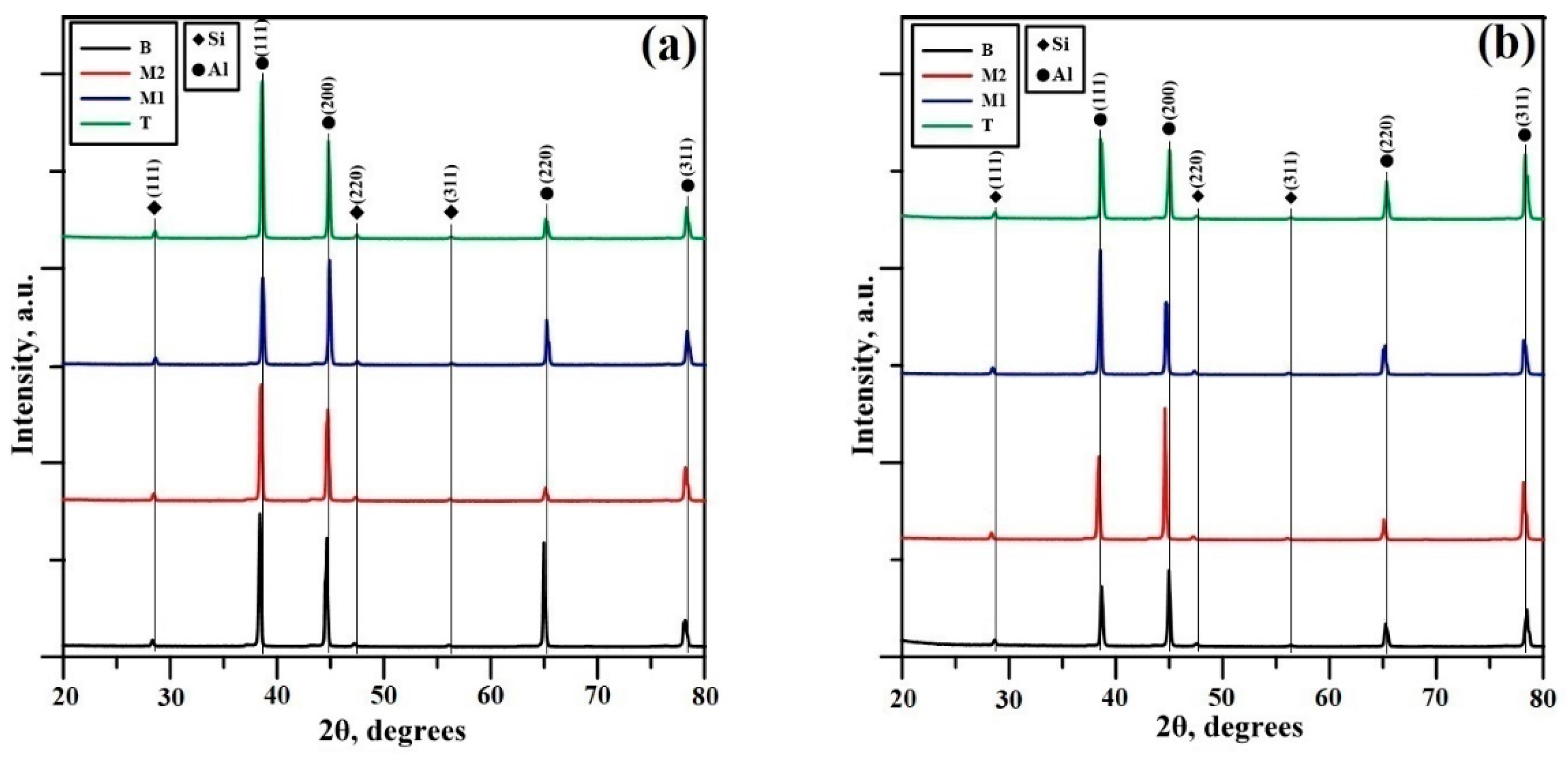
- Both specimens have a double phase composition consisting of aluminum and silicon peaks with a face-centered cubic structure. The preferred crystallographic orientation of the specimen built at a speed of 13.3 mm/s is initially directed towards the (220) plane followed by a 45° unit cell shift towards the (200) crystallographic plane. In the case of a welding speed of 20 mm/s a preorientation from the (200) plane towards the (311) plane is observed towards the top of the specimen due to the increase of the deposition temperature. An increase of the FWHM, thus the concentration of defects, is observed parallel to the increase of the height of the specimens;
- (2)
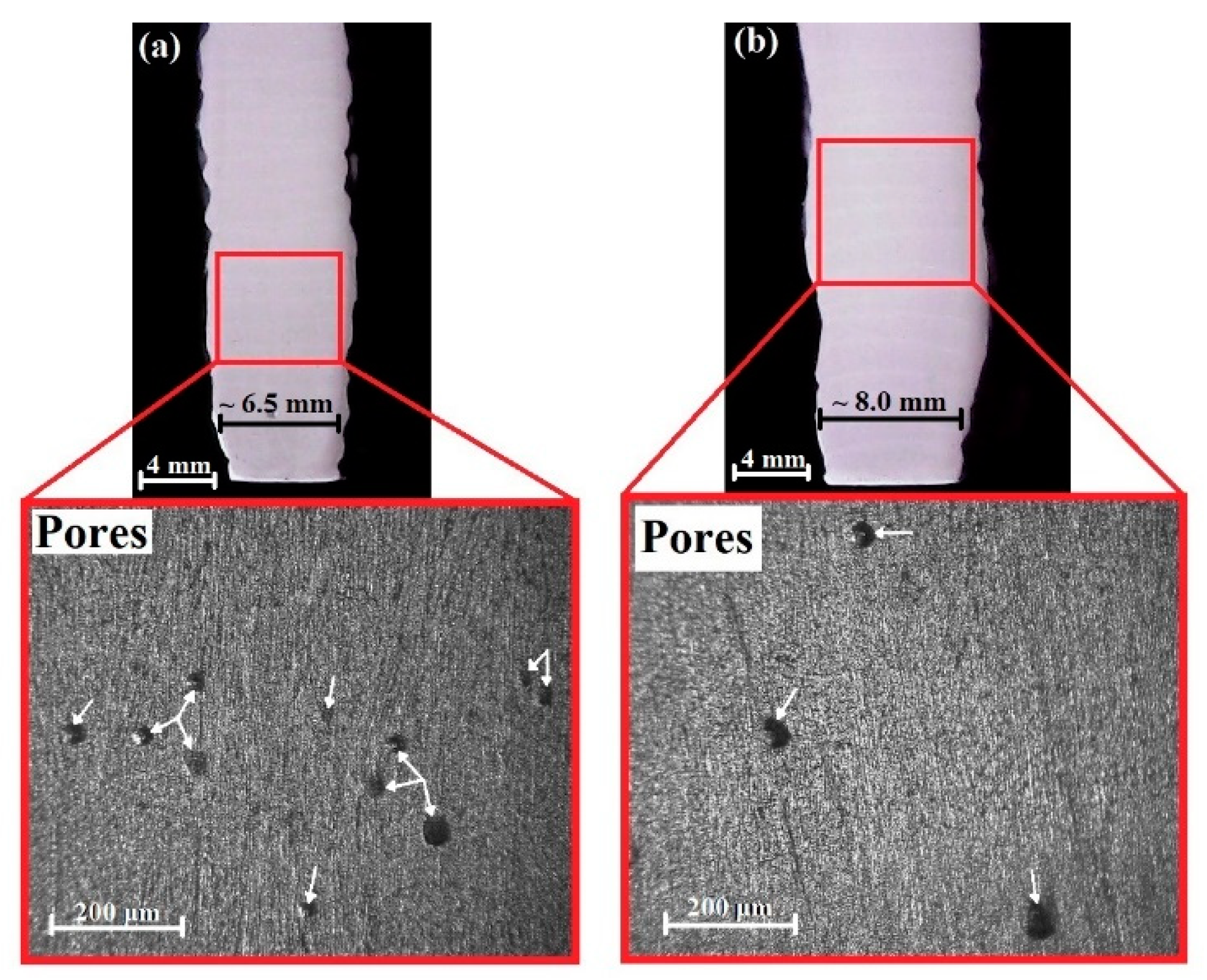
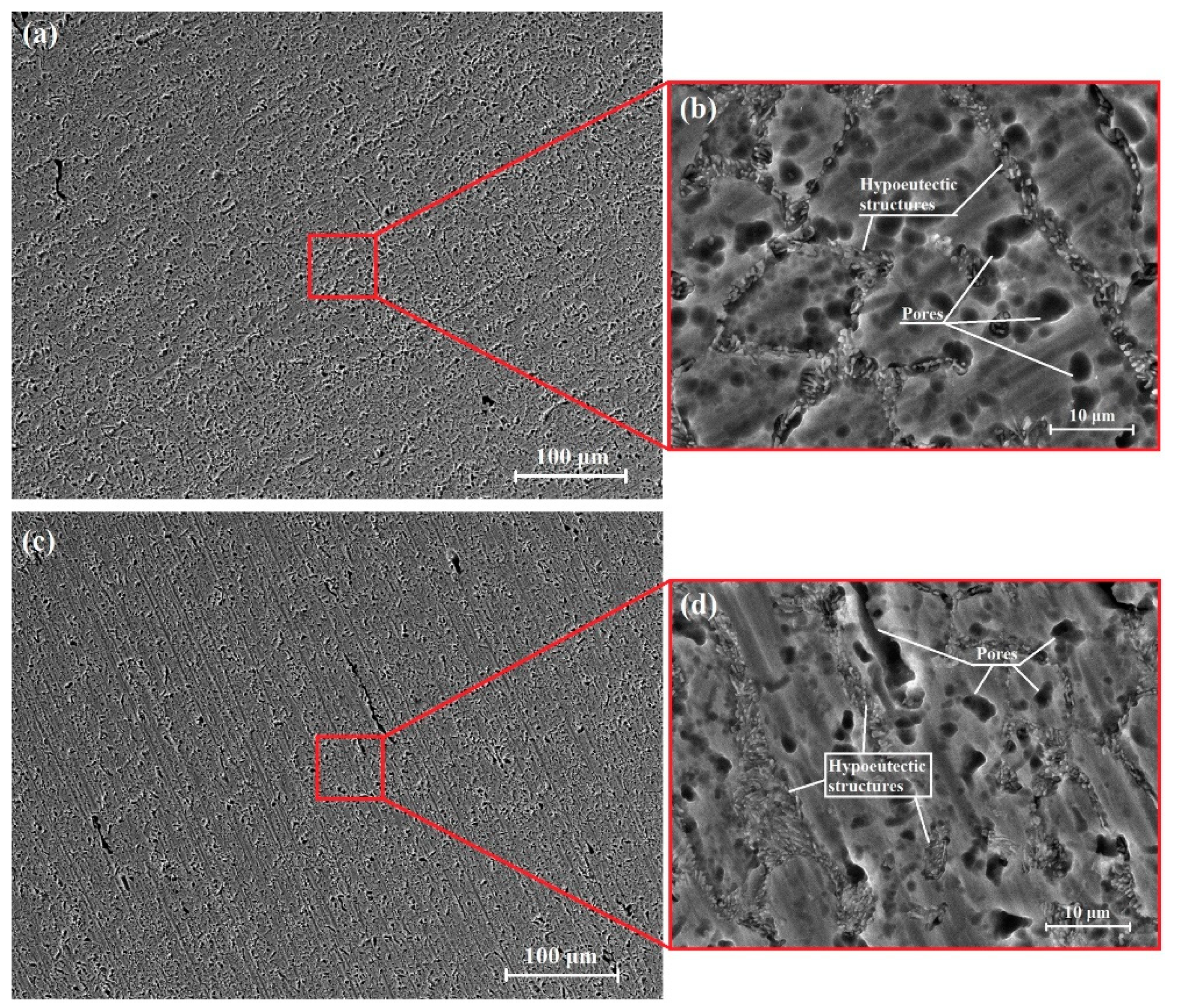
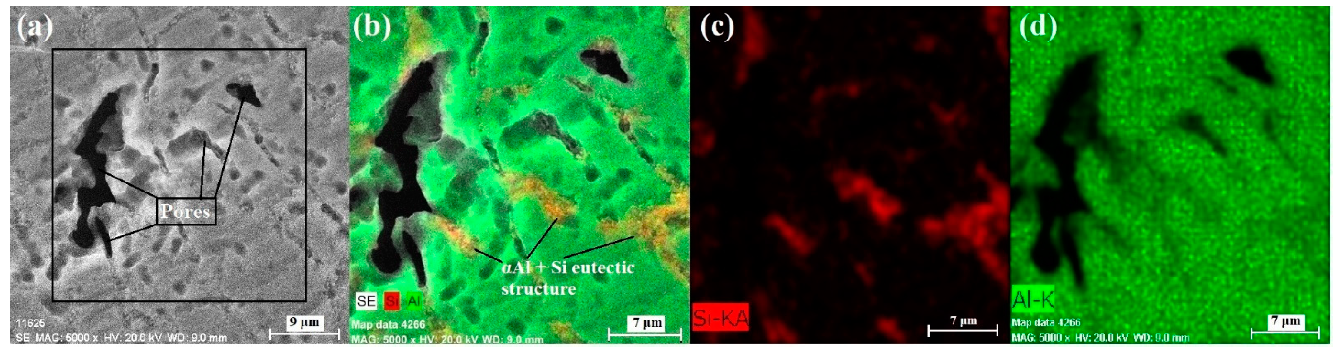
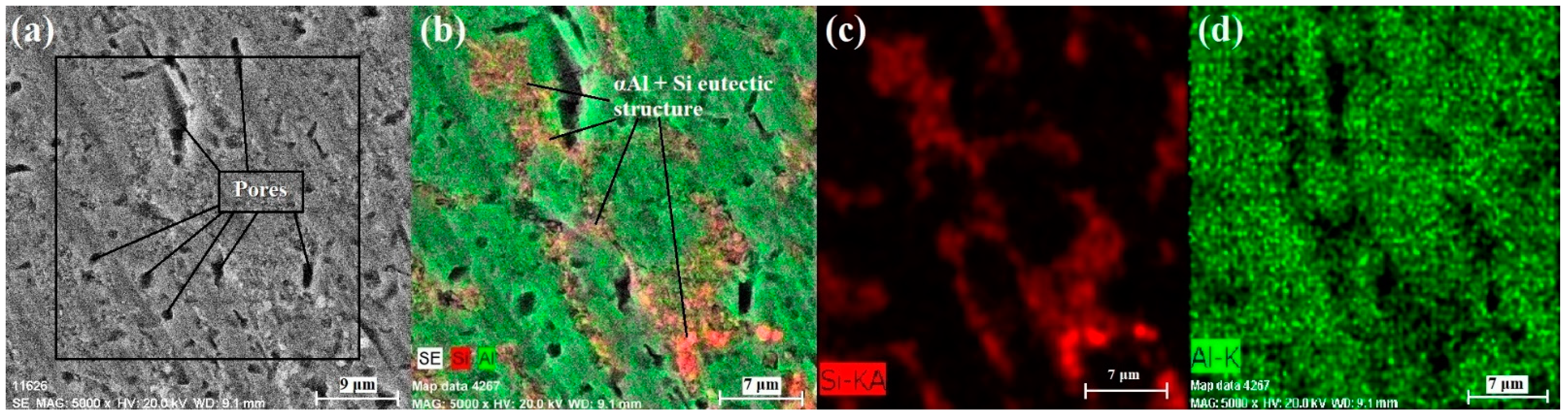
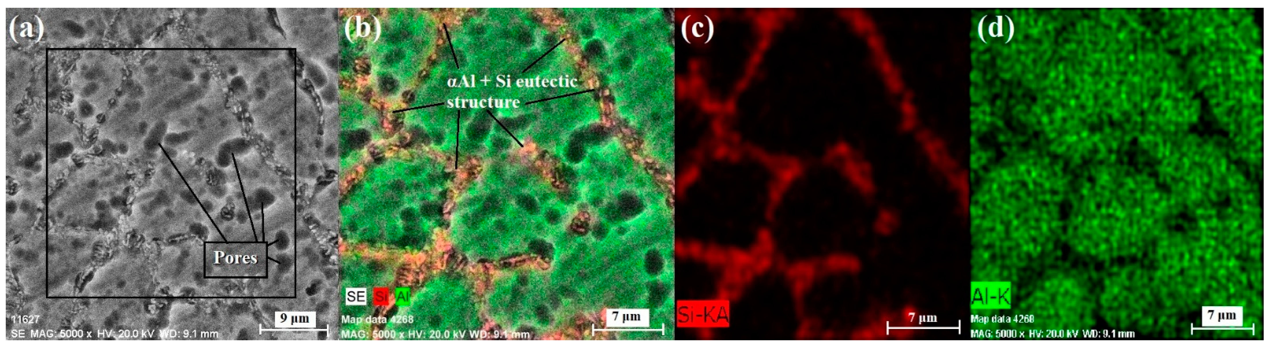
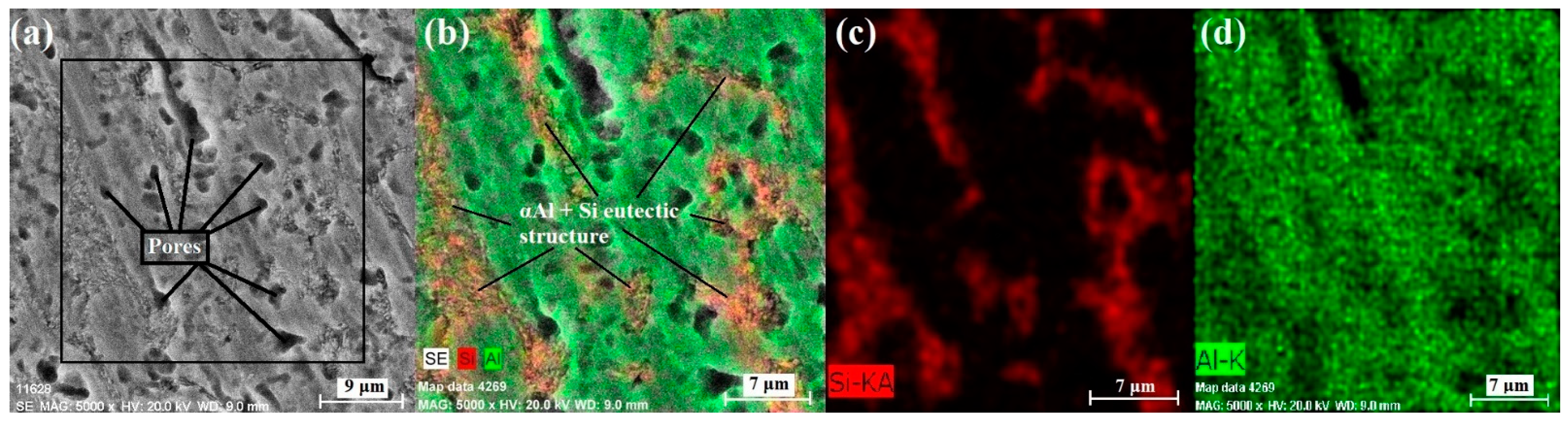
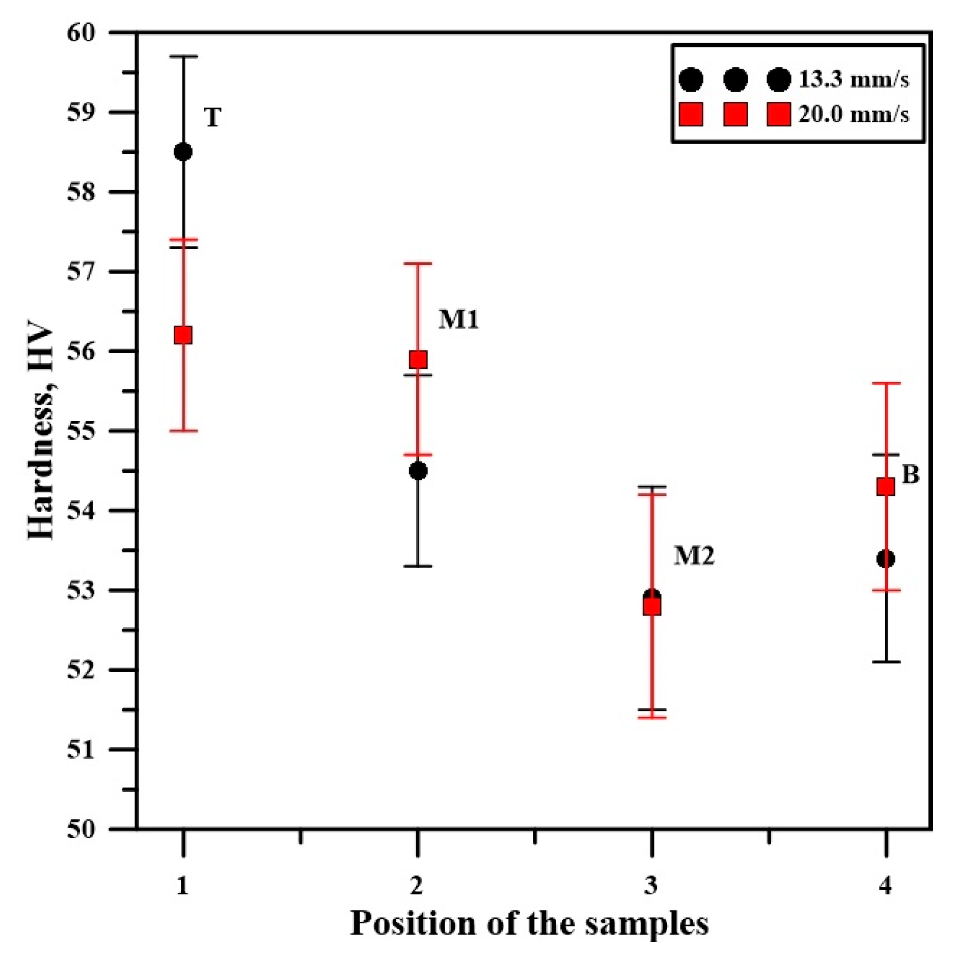
- The lowering of the welding speed resulted in an increase of the thickness of the specimens. The density of αAl + Si eutectic formations in their structure was also increased. In addition, the lower welding speed increased the volume of the melt pool and the lifetime of liquid phase respectively, which improved the diffusion of gases and thus led to the decrease of the concentration of pores in the structure of the specimens;
- (3)
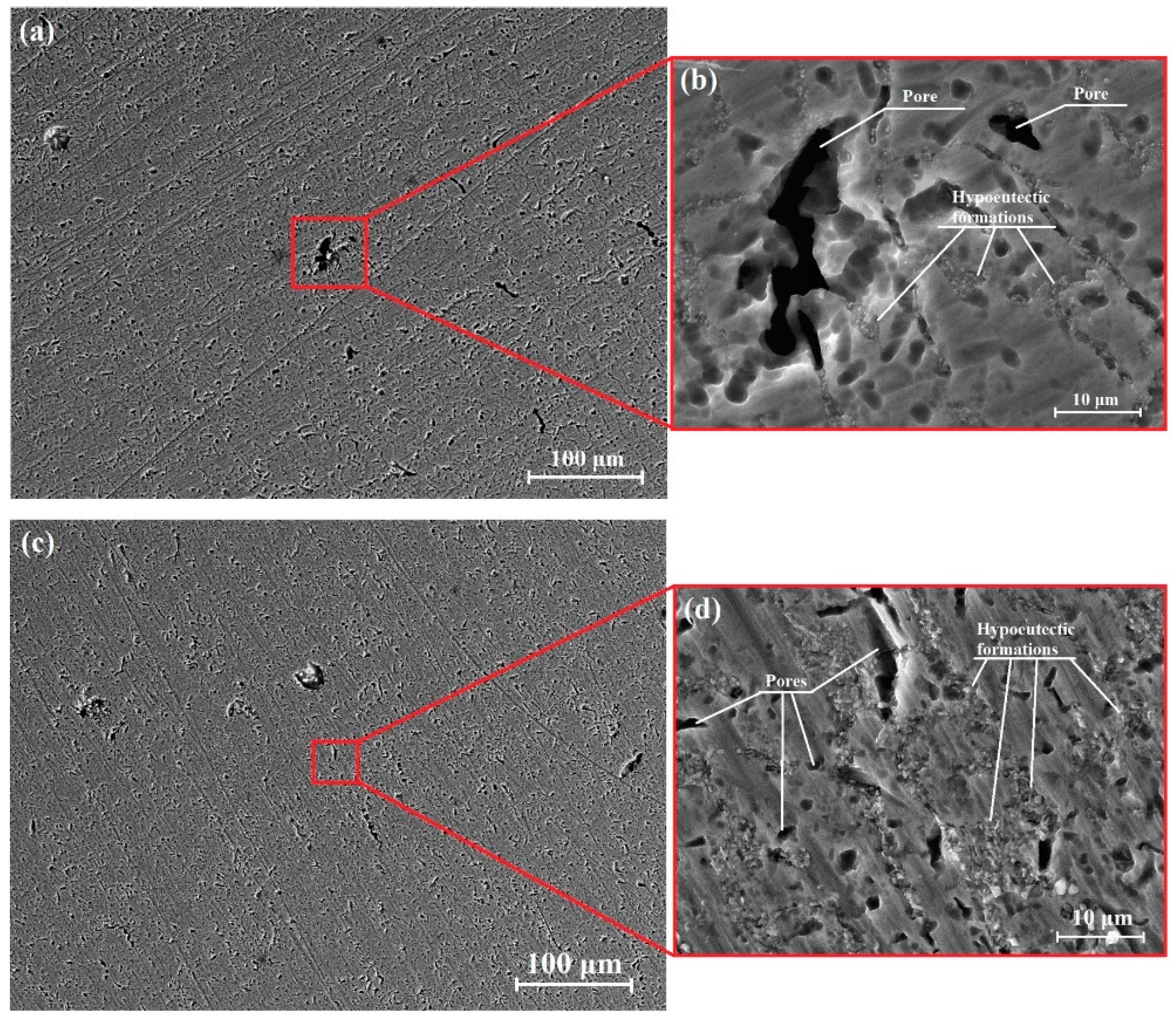
- Irregularly structured eutectic formations were observed at the initial stages of specimen growth in both cases. Since the deposition temperature increased at the more advanced stages of growth a higher cooling rate was observed, which led to the faster solidification of the melt pool. As it is known aluminum has a higher heat of fusion and a higher thermal conductivity compared to silicon, which explains its’ higher solidification rate. This causes a change in the structure of the αAl + Si eutectic formations from irregular to fibrous. The newly formed fibers occupy the space between the aluminum polycrystalline grains, where most of the defects in the structure are formed. This leads to the decrease of the mobility of defects in the aluminum matrix, which leads to the increase of the coefficient of elastic deformation. This intern leads to the slight increase of the hardness of the specimens.
Author Contributions
Funding
Data Availability Statement
Conflicts of Interest
References
- Herzog, D.; Seyda, V.; Wycisk, E.; Emmelmann, C. Additive manufacturing of metals. Acta Mater. 2016, 117, 371–392. [Google Scholar] [CrossRef]
- Ngo, T.; Kashani, A.; Imbalzano, G.; Nguyen, K.; Hui, D. Additive manufacturing (3D printing): A review of materials, methods, applications and challenges. Compos. Part B 2018, 143, 172–196. [Google Scholar] [CrossRef]
- Frazier, W. Metal Additive Manufacturing: A Review. J. Mater. Eng. Perf. 2014, 23, 1917–1928. [Google Scholar] [CrossRef]
- DebRoy, T.; Wei, H.; Zuback, J.; Mukherjee, T.; Elmer, J.; Milewski, J.; Beese, A.; Wilson-Heid, A.; De, A.; Zhang, W. Additive manufacturing of metallic components—Process, structure and properties. Prog. Mater. Sci. 2018, 92, 112–224. [Google Scholar] [CrossRef]
- Wu, B.; Pan, Z.; Ding, D.; Cuiuri, D.; Li, H.; Xu, J.; Norrish, J. A review of the wire arc additive manufacturing of metals: Properties, defects and quality improvement. J. Manuf. Process. 2018, 35, 127–139. [Google Scholar] [CrossRef]
- Ramalho, A.; Santos, T.; Bevans, B.; Smoqi, Z.; Rao, P.; Oliveira, J. Effect of contaminations on the acoustic emissions during wire arc additive manufacturing of 316L stainless steel. Add. Manuf. 2022, 51, 102585. [Google Scholar] [CrossRef]
- Rodrigues, T.; Escobar, J.; Shen, J.; Duarte, V.; Ribamar, G.; Avila, J.; Maawad, E.; Schell, N.; Santos, T.; Oliveira. Effect of heat treatments on 316 stainless steel parts fabricated by wire and arc additive manufacturing: Microstructure and synchrotron X-ray diffraction analysis. Add. Manuf. 2021, 48, 102428. [Google Scholar] [CrossRef]
- Li, S.; Li, J.; Jiang, Z.; Cheng, Y.; Li, Y.; Tang, S.; Leng, J.; Chen, H.; Zou, Y.; Zhao, Y.; et al. Controlling t he columnar-to-equiaxed transition during Directed Energy Deposition of Inconel 625. Add. Manuf. 2022, 57, 102958. [Google Scholar] [CrossRef]
- Hauser, T.; Reisch, R.; Breese, P.; Lutz, B.; Pantano, M.; Nalam, Y.; Bela, K.; Kamps, T.; Volpp, J.; Kaplan, A. Porosity in wire arc additive manufacturing of aluminum alloys. Addit. Manuf. 2021, 41, 101993. [Google Scholar] [CrossRef]
- Norrish, J.; Cuiuri, D. The controlled short circuit GMAW process: A tutorial. J. Manuf. Process. 2014, 16, 86–92. [Google Scholar] [CrossRef]
- Kah, P.; Suoranta, R.; Martikainen, J. Advanced gas metal arc welding processes. Int. J. Adv. Manuf. Technol. 2013, 67, 655–674. [Google Scholar] [CrossRef]
- Ayarkwa, K.; Williams, S.; Ding, J. Investigation of pulse advance cold metal transfer on aluminum wire arc additive manufacturing. Int. J. Rapid. Manuf. 2015, 5, 44–57. [Google Scholar] [CrossRef]
- Chen, T.; Xue, S.; Wang, B.; Zhai, P.; Long, W. Study on Short-Circuiting GMAW Pool Behaviour and Microstructure of the Weld with Different Waveform Control Methods. Metals 2019, 9, 1326. [Google Scholar] [CrossRef]
- Matusiak, J.; Pfeifer, T. The research of technological and environmental conditions during low-energetic gas-shielded metal arc welding of aluminum alloys. Welding Int. 2013, 27, 338–344. [Google Scholar] [CrossRef]
- Kumar, M.; Manikandan, M. Assessment of Process, Parameters, Residual Stress Mitigation, Post Treatments and Finite Element Analysis Simulations of Wire Arc Additive Manufacturing Technique. Met. Mater. Int. 2022, 28, 54–111. [Google Scholar] [CrossRef]
- Veiga, F.; Suarez, A.; Aldalur, E.; Bhujangrao, T. Effect of the Metal Transfer Mode on the Symmetry of Bead Geometry in WAAM Aluminum. Symmetry 2021, 13, 1245. [Google Scholar] [CrossRef]
- Köhler, M.; Fiebig, S.; Hensel, J. Wire and Arc Additive Manufacturing of Aluminum Components. Metals 2019, 9, 608. [Google Scholar] [CrossRef]
- Köhler, M.; Hensel, J.; Dilger, K. Effects of Thermal Cycling on Wire and Arc Additive Manufacturing of Al-5356 Components. Metals 2020, 10, 952. [Google Scholar] [CrossRef]
- Geng, Y.; Panchenko, I.; Chen, X.; Ivanov, Y.; Konovalov, S. Investigation of Microstructure and Fracture Mechanism of Al-5.0Mg Alloys Fabricated by Wire Arc Additive Manufacturing. J. Mater. Eng. Perf. 2021, 30, 7406–7416. [Google Scholar] [CrossRef]
- Sun, J.; Hensel, J.; Köhler, M.; Dilger, K. Residual stress in wire and arc additively manufactured aluminum components. J. Mater. Process. 2021, 65, 97–111. [Google Scholar] [CrossRef]
- Su, C.; Chen, X.; Konovalov, S.; Singh, R.; Jayalakshmi, S.; Huang, L. Effect of Deposition Strategies on the Microstructure and Tensile Properties of Wire Arc Additive Manufactured Al-5Si Alloys. J. Mater. Eng. Perf. 2021, 30, 2136–2146. [Google Scholar] [CrossRef]
- Valkov, S.; Kotlarski, G.; Ormanova, M.; Doynov, N.; Ossenbring, R.; Petrov, P.; Michailov, V. Crystallographic structure and mechanical properties of wire arc additively manufactured Al5356 components. C. R. Acad. Bulg. Sci. 2021, 74, 820–827. [Google Scholar] [CrossRef]
- He, D.; Zhao, Y.; Daemen, L.; Qian, J.; Lokshin, K.; Shen, T.; Zhang, J.; Lawson, A. Thermoelastic and texture behavior of aluminum at high pressure and high temperature investigated by in situ neutron diffraction. J. Appl. Phys. 2004, 95, 4645–4650. [Google Scholar] [CrossRef]
- Wang, X.; Shen, B.; Deng, L.; Li, J. Effects of original orientation combination on substructure characteristics during continuous dynamic recrystallization in an extruded Al-Cu-Li alloy. Mat. Char. 2017, 130, 113–122. [Google Scholar] [CrossRef]
- Vashista, M.; Paul, S. Correlation between full width at half maximum (FWHM) of XRD peak with residual stress on ground surfaces. Phil. Mag. 2012, 92, 4194–4204. [Google Scholar] [CrossRef]
- Tawfik, M.; Nemat-Alla, M.; Dewidar, M. Enhancing the properties of aluminum alloys fabricated using wire + arc additive manufacturing technique—A review. J. Mater. Res. Tech. 2021, 13, 754–768. [Google Scholar] [CrossRef]
- Nikanorov, S.P.; Volkov, M.; Gurin, V.; Burenkov, Y.; Derkachenko, L.; Kardashev, B.; Regel, L.; Wilcox, W. Structural and mechanical properties of Al-Si alloys obtained by fast cooling of a levitated melt. Mat. Sci. Eng. A 2005, 390, 63–69. [Google Scholar] [CrossRef]
- Tian, Y.; Shen, J.; Hu, S.; Wang, Z.; Gou, J. Microstructure and mechanical properties of wire and arc additive manufactured Ti-6Al-4V and AlSi5 dissimilar alloys using cold metal transfer welding. J. Manuf. Process. 2019, 46, 337–344. [Google Scholar] [CrossRef]
- Neuser, M.; Grydin, O.; Frolov, Y.; Schaper, M. Influence of solidification rates and heat treatment on the mechanical performance and joinability of the cast aluminum alloy AlSi10Mg. Prod. Eng. 2022, 16, 193–202. [Google Scholar] [CrossRef]
- Lee, T.; Kim, C.; Kang, M. Effects of Electrode Negative Pulsing Ration in Direct Energy Deposition via Variable-Polarity Cold Metal Transfer Process on the Deposition Behavior and Microstructural Characteristics. Metals 2022, 12, 475. [Google Scholar] [CrossRef]
- Makhlouf, M.; Guthy, H. The aluminum-silicon eutectic reaction: Mechanisms and crystallography. J. Light Met. 2001, 1, 199–218. [Google Scholar] [CrossRef]
- Barrirero, J. Eutectic Modification of Al-Si Casting Alloys; Linköping University: Linköping, Sweden, 2019. [Google Scholar]
- Sjölander, S.; Seifeddine, S. The heat treatment of Al-Si-Cu-Mg casting alloys. J. Mater. Process. 2010, 210, 1249–1259. [Google Scholar] [CrossRef]


| Alloy | Al | Si | Fe | Cu | Mn | Mg | Zn | Be | Ti | Cr | Others |
|---|---|---|---|---|---|---|---|---|---|---|---|
| AlSi5 | Bal. | 4.5–5.5 | 0.6 | 0.3 | 0.15 | 0.2 | 0.1 | 0.0003 | 0.15 | - | 0.15 |
| Al6082T6 | Bal. | 1.2 | 0.5 | 0.1 | 0.4 | 0.6 | 0.2 | - | 0.1 | 0.25 | 0.15 |
| Position in the Specimen | Phkl, % | |||
|---|---|---|---|---|
| P111 | P200 | P220 | P311 | |
| 13.3 mm/s | ||||
| T | 26.8 | 35.4 | 15.5 | 22.3 |
| M1 | 13.2 | 33.9 | 31.3 | 21.6 |
| M2 | 22.7 | 37.9 | 12.0 | 27.4 |
| B | 14.0 | 24.4 | 49.8 | 11.8 |
| 20.0 mm/s | ||||
| T | 11.9 | 22.0 | 25.9 | 40.2 |
| M1 | 22.3 | 27.7 | 24.0 | 26.0 |
| M2 | 11.9 | 40.1 | 13.6 | 34.4 |
| B | 12.6 | 33.6 | 21.8 | 32.0 |
| Material and Detected Plane | FWHM | |||
|---|---|---|---|---|
| 13.3 mm/s | ||||
| T | M1 | M2 | B | |
| Al (111) | 0.2601 | 0.2618 | 0.2111 | 0.2120 |
| Al (200) | 0.2615 | 0.2108 | 0.2616 | 0.2626 |
| Al (220) | 0.3141 | 0.2626 | 0.3151 | 0.2411 |
| Al (311) | 0.3677 | 0.4202 | 0.3151 | 0.4220 |
| 20.0 mm/s | ||||
| Al (111) | 0.2624 | 0.2133 | 0.2101 | 0.2121 |
| Al (200) | 0.2626 | 0.2625 | 0.2112 | 0.2107 |
| Al (220) | 0.2636 | 0.3151 | 0.3193 | 0.3677 |
| Al (311) | 0.3676 | 0.3677 | 0.2628 | 0.3151 |
Publisher’s Note: MDPI stays neutral with regard to jurisdictional claims in published maps and institutional affiliations. |
© 2022 by the authors. Licensee MDPI, Basel, Switzerland. This article is an open access article distributed under the terms and conditions of the Creative Commons Attribution (CC BY) license (https://creativecommons.org/licenses/by/4.0/).
Share and Cite
Kotlarski, G.; Ormanova, M.; Ossenbrink, R.; Nikitin, A.; Doynov, N.; Valkov, S.; Michailov, V. Fabrication and Characterization of Wire Arc Additively Manufactured AlSi5 Structures. Metals 2022, 12, 1870. https://doi.org/10.3390/met12111870
Kotlarski G, Ormanova M, Ossenbrink R, Nikitin A, Doynov N, Valkov S, Michailov V. Fabrication and Characterization of Wire Arc Additively Manufactured AlSi5 Structures. Metals. 2022; 12(11):1870. https://doi.org/10.3390/met12111870
Chicago/Turabian StyleKotlarski, Georgi, Maria Ormanova, Ralf Ossenbrink, Alexander Nikitin, Nikolay Doynov, Stefan Valkov, and Vesselin Michailov. 2022. "Fabrication and Characterization of Wire Arc Additively Manufactured AlSi5 Structures" Metals 12, no. 11: 1870. https://doi.org/10.3390/met12111870
APA StyleKotlarski, G., Ormanova, M., Ossenbrink, R., Nikitin, A., Doynov, N., Valkov, S., & Michailov, V. (2022). Fabrication and Characterization of Wire Arc Additively Manufactured AlSi5 Structures. Metals, 12(11), 1870. https://doi.org/10.3390/met12111870