Abstract
This study investigates the effect of gate insulators on thin-film transistors (TFTs) using an amorphous InGaZnO4 (a-IGZO) channel layer. TFTs with single-layer Ta2O5 and dual-layer Ta2O5/SiO2 gate insulators were fabricated on a glass substrate. An evaluation of the insulating film using the MIM (Metal-Insulator-Metal) structure confirmed its electrical characteristics. Microscopic imaging showed that the dual-layer Ta2O5/SiO2 dielectric significantly improved surface characteristics. A reduction in the leakage current, better on/off ratios, and a decreased subthreshold swing (SS) compared to a single-layer Ta2O5 dielectric were reported. The dual-layer insulator composed of SiO2/Ta2O5 was highly effective in improving device characteristics.
1. Introduction
Oxide semiconductor materials have emerged as novel candidates for large-area silicon devices. In particular, amorphous InGaZnO4 (a-IGZO), a transparent amorphous oxide semiconductor, has attracted considerable attention because of its high electron mobility [1,2,3,4]. In addition, Nomura et al. and Yabuta et al. demonstrated the fabrication of high-performance amorphous a-IGZO thin-film transistors (TFTs) using pulsed laser deposition [1] and RF sputtering [3]. a-IGZO has a carrier mobility of 10 cm2/(Vs) or more and can control the carrier concentration even in the amorphous phase [5]. This mobility value is much higher than organic or other amorphous oxide semiconductors. This high mobility is due to the overlap of the ns-orbital of the metal cation, being larger than the 2p-orbital of the oxygen anion; a-IGZO exhibits high mobility while having an amorphous structure.
The utilization of a-IGZO TFTs as switching elements in flat-panel displays, such as liquid-crystal displays (LCDs), organic light-emitting diode displays, and electronic paper, is of particular interest [6,7,8]. Currently, hydrogenated amorphous silicon (a-Si:H) TFTs are commonly used as switching elements in the display industry. Although both a-IGZO and a-Si:H are amorphous semiconductors, they differ in their material properties; including the carrier generation mechanisms and the chemical bonding structures. Understanding the key features of a-IGZO TFT, which are different from the existing a-Si:H TFT, is important for commercial use of a-IGZO [9,10,11]. However, the carrier movement of semiconductor materials greatly affects device performance. It is essential to remove these defects [12]; in addition, electrical contact between the channel and source/drain also determines the electrical performance of the device. For this purpose, an additional heat treatment process is required [13].
In consideration of this, research on various gate dielectric film materials (HfO2 [14], Al2O3 [15,16], Ta2O5 [17,18], Y2O3 [19], and ZrO2 [20]) has been conducted in order to improve the performance of the transistor.
SiO2 has long been the gate dielectric material selected for silicon device applications due to its excellent materials and interfacial properties, including: (i) device-quality films that can be grown directly on silicon; (ii) a large energy band gap (~9 eV) [21]; (iii) relatively large conduction and valence band offset energies with respect to Si (~3.2 eV and 4.5 eV, respectively); (iv) high effective electrical resistivity (1015–1017 Ωcm); (v) excellent dielectric breakdown strength (>107 V/cm); (vi) low bulk and interface defect densities (<1016 cm−3 and <1011 cm−2, respectively); and (vii) excellent thermal stability in contact with crystalline Si [22]. These studies show that device performance is limited by the tunneling leakage current through ultrathin (< 2 nm) SiO2 dielectrics, which are required in the devices with aggressively scaled gate lengths. Recently, high-K oxides containing transition metals or rare earth elements (including ternary silicate and aluminate phases) have attracted attention as alternatives to conventional gate dielectrics [23]. High-K gate dielectrics can potentially provide comparable device performance with a much thicker dielectric layer, thereby significantly reducing tunneling leakage currents. A comprehensive study of all known elemental and multi-component oxides using a thermodynamic approach identified several high-K gate dielectric candidates with excellent silicon compatibility [24,25]. Among high-k gate dielectric materials, Ta2O5 is one of the most promising materials due to its high dielectric constant (22~60), low leakage current, excellent dielectric breakdown strength, thermal and chemical stability, and other properties. Moreover, in order to be applied to a flexible substrate of a transistor device, the factor of temperature cannot be ignored. Conventional chemically deposited organic dielectrics give good results for transistor properties; however, they require slow and high temperatures in growth and curing processes to form organic thin films [26,27]. In order to solve these factors, attempts have been made to manufacture a dielectric capable of low-temperature processing using rf magnetron sputtering. However, in the case of a thin film prepared in this way, it affects the growing film and its interface [28,29,30,31,32]. In the electrical characteristics of IGZO TFT, reduction of leakage current, improvement of surface roughness, and reduction of charge trapping density are essential factors. In order to solve these factors, considering the physical and low-temperature processes, the interface quality of the high-temperature process, SiO2, is excellent. In addition, most high dielectric constants exhibit polycrystalline structures and rough surfaces; which can contribute to reduced reliability and degraded interfacial properties. Furthermore, high-k dielectrics typically exhibit a lower bandgap and smaller band offset (by semiconductors) than conventional SiO2; this results in lower breakdown voltages and higher leakage currents.
The overall performance of the transistor is very dependent on the gate insulating film; and it is necessary to apply a high-k, high-k thin film to drive the transistor at a low voltage. The conventional gate insulating film mainly uses a SiO2 thin film through a high-temperature process. However, for application to devices requiring a lower process temperature, an alternative insulating film or process technology is essential. However, when using a high-k gate insulating film, there may be disadvantages in that the leakage current is high and the breakdown voltage is lowered in terms of electrical performance due to the relatively lower band gap and band offset than that of SiO2; as well as the polycrystalline structure and surface roughness. Due to these factors, studies on double stacking [17,18], multi-layer [33], and multi-component structures [34] using high-k gate materials and conventional SiO2 materials have recently been conducted. Therefore, instead of using one type of high-k gate insulating film, it is necessary to secure an oxide TFT with high mobility and stable characteristics by using the existing SiO2 and SiNx insulating film, and a study on the stacked structure of the high-k insulating film. In order to secure transistor characteristics even in low-temperature processes and thin thicknesses, we developed an oxide transistor with a dual structure of gate insulating film of low-temperature process SiO2 and room temperature process high dielectric constant Ta2O5 thin film.
2. Materials and Methods
The oxide transistor constructed for this study had a bottom-gate structure. A glass plate (5 cm × 5 cm) was used as the substrate. Molybdenum (Mo) was used to construct the gate, source, and drain electrodes. For the deposition of Mo thin films, a Mo target (4-inch diameter) was sputtered with argon (Ar) at room temperature using a DC sputtering system. The base and working pressures of the sputtering chamber were 4.3 x 10⁻⁵ Torr and 6.7 mTorr, respectively. The applied DC power was 100 W, and the thickness of all the Mo thin films was controlled at 150 nm. The Mo thin films were carefully deposited as the source and drain electrodes after the deposition of the a-IGZO films. Mo thin films provide ohmic contact with the a-IGZO semiconductor layer and have negligible contact resistance [35].
An a-IGZO thin film, which forms the semiconductor layer, was deposited via RF magnetron sputtering. A ceramic InGaZnO4 target (2-inch diameter) was sputtered using Ar plasma at room temperature. The thickness of the a-IGZO layer was controlled at 30 nm. The substrate and the target were 7 cm apart; and the substrate holder rotated at 1 rpm to ensure the uniformity of the deposited thin films. During sputtering, the RF power, chamber pressure, O2 flow rate, and Ar flow rate were maintained at 100 W, 10 mTorr, 6 sccm, and 54 sccm, respectively.
A Ta2O5 film (30 nm thick) was deposited on the substrate using RF magnetron sputtering. During the deposition process, the O2 ratio was maintained at 30%; and the deposition rate was 3 nm/min. The RF power, chamber pressure, O2 flow rate, and Ar flow rate were maintained at 100 W, 2 mTorr, 6 sccm, and 14 sccm, respectively.
SiO2 film (30 nm thick) was deposited on the substrate using a plasma-enhanced chemical vapor deposition (PECVD) system. During sputtering, the RF power, SiH4 and N2O flow rates, and temperature were maintained at 140 W, 4 sccm, 2000 sccm, and 300 °C, respectively.
All the patterning processes, except for defining the source and the drain, were performed using photolithography. The gate length and width of the fabricated a-IGZO TFT were 7 μm and 100 μm, respectively. Post-heat treatment of some transistors was performed in conventional thermal treatment equipment (tube furnace, OTF-1200X, MTI, Richmond, CA, USA) at 300 °C for 2 h in the state of continuously injecting oxygen.
The thickness and microstructures of the a-IGZO thin films were observed using a field emission scanning electron microscope (FE-SEM, Nova Nano SEM 200, FEI, Hillsboro, OR, USA). X-ray diffraction (XRD, Dmax2500/PC) analysis was conducted to obtain information on the structure of the crystalline material. The leakage current densities and electrical properties of the TFTs were measured using a Keithley 4200A-SCS source measure unit. All the electrical properties were measured in the dark.
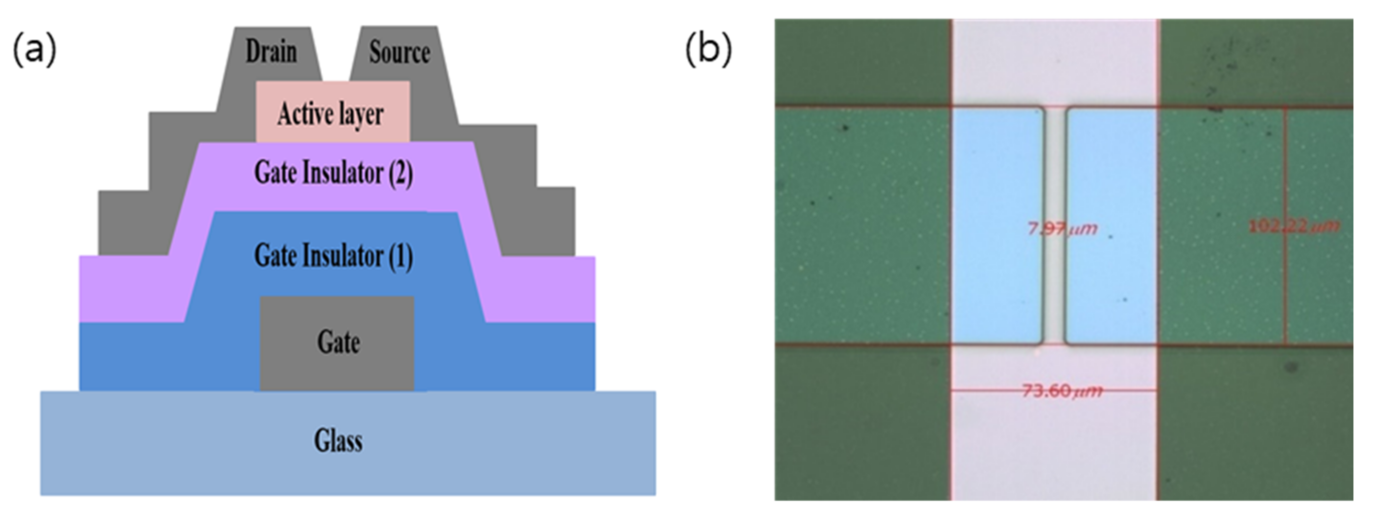
Figure 1a gives a schematic description of a dual-layer gate insulator in the a-IGZO transistor. The optical microscope results, as shown in Figure 1b, confirmed that the width and the length of the channel are 100 μm and 7 μm, respectively.
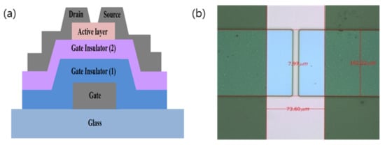
Figure 1.
(a) Schematic structure of a-IGZO TFT with a dual-layer gate insulator. (b) Top view of the channel using an optical microscope.
3. Results
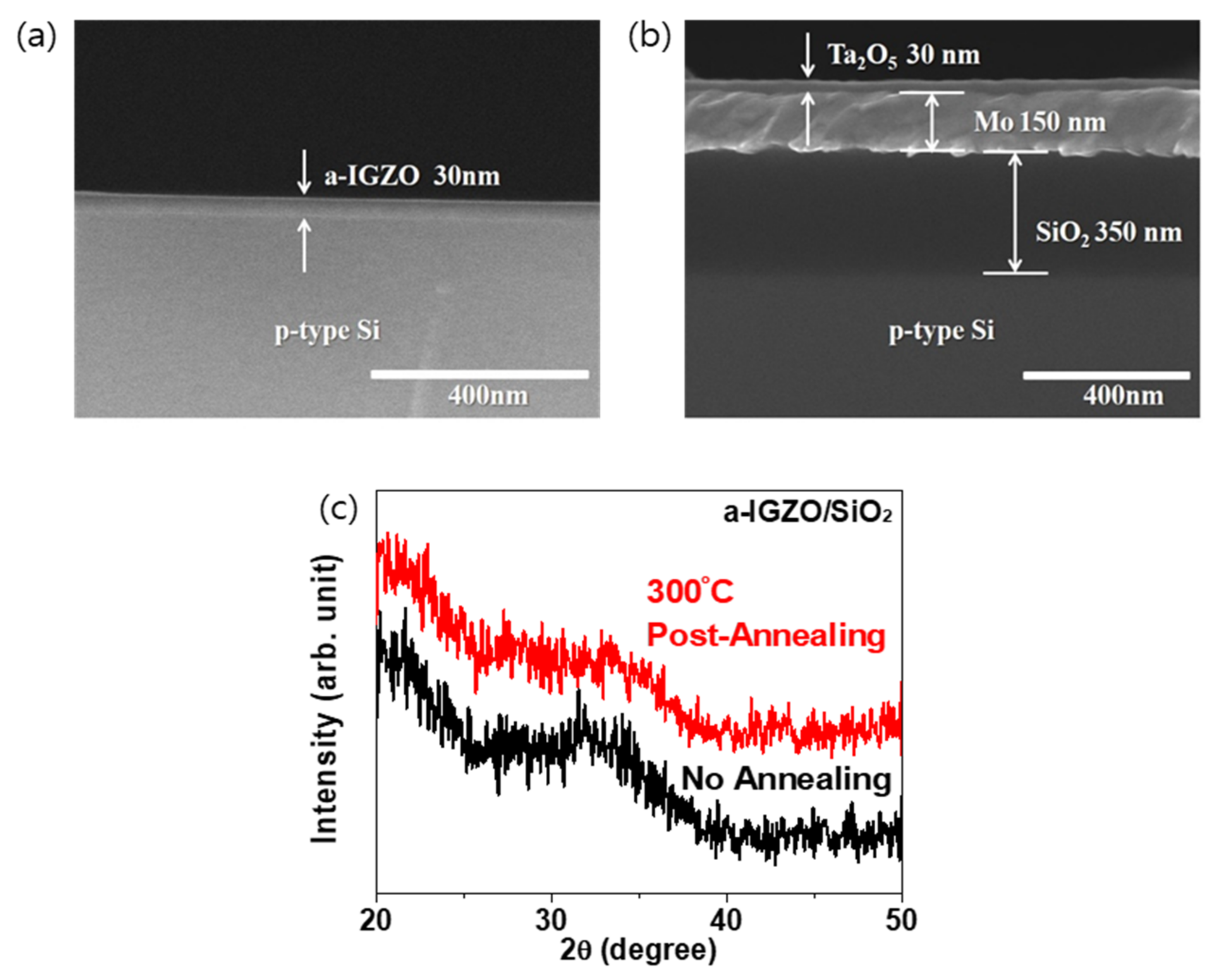
The a-IGZO/Si/SiO2 and Ta2O5/Mo/SiO2/Si structures were confirmed by SEM. FE-SEM imaging (Figure 2a,b) confirmed that the a-IGZO film of the channel layer and the Ta2O5 film of the gate insulator layer were 30 nm thick and the electrode Mo was 150 nm thick. Figure 2c shows the XRD pattern of an a-IGZO layered structure grown on a Si/SiO2 substrate. In order to confirm the change of the IGZO film before and after the heat treatment, the samples that were not heat treated and the samples that were heat treated at 300 °C for 2 h in an oxygen atmosphere were analyzed. Two halo peaks were observed at around 22° and 34°.

Figure 2.
(a) The cross-sectional FE-SEM image of the a-IGZO/SiO2/Si structure; (b) the Ta2O5/Mo/SiO2/Si structure; and (c) an XRD pattern of the a-IGZO/SiO2 layered structure grown on a Si substrate by sputtering.
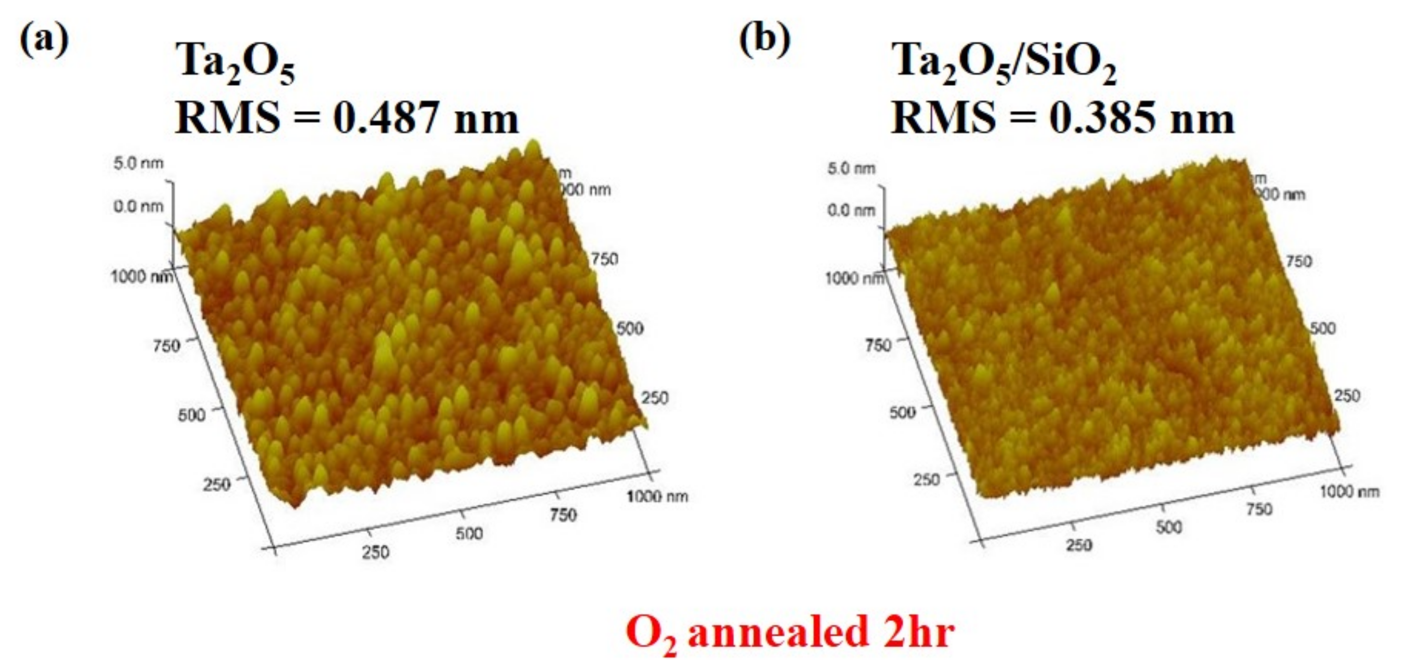
Figure 3a,b show the surface characteristics of Ta2O5 (60 nm) and SiO2/Ta2O5 (30 nm/30 nm). We can see that the surface properties were improved by depositing SiO2 at the bottom and Ta2O5 at the top. The dual-structure SiO2/Ta2O5 (30 nm/30 nm) thin-film had an RMS characteristic of 0.385 nm, which was reduced by about 21% compared to the surface characteristic of the Ta2O5 single layer of 0.487 nm.

Figure 3.
AFM image of: (a) the Ta2O5 film and (b) the SiO2/Ta2O5 film grown on a Si substrate.
Because the electric field-induced carrier is confined to a narrow region close to the interface between the gate-insulating film and the channel layer, the characteristics of the interface have a significant influence on the TFT characteristics. The surface of a rough gate-insulating film may result in more grain boundaries [36] or in an increased number of trap states [37]; which may cause surface scattering [38] and reduce the mobility of the carrier.
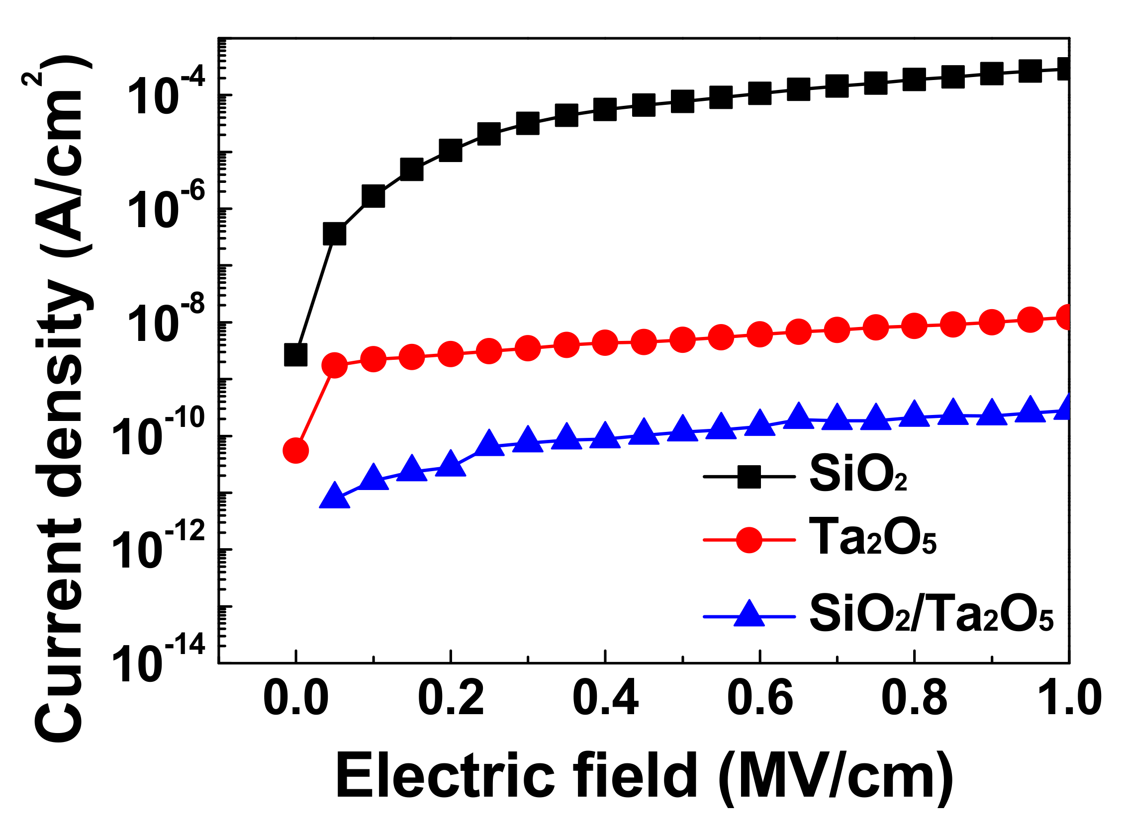
The leakage current densities of the SiO2 (60 nm), Ta2O5 (60 nm), and SiO2/Ta2O5 (30 nm/30 nm) dielectric films are shown in Figure 4. As can be seen, the leakage current density is clearly improved by depositing the SiO2 thin film before the Ta2O5 thin film deposition.

Figure 4.
Leakage current densities of the SiO2 (60 nm), Ta2O5 (60 nm), and SiO2/Ta2O5 (30 nm/30 nm) dielectric films.
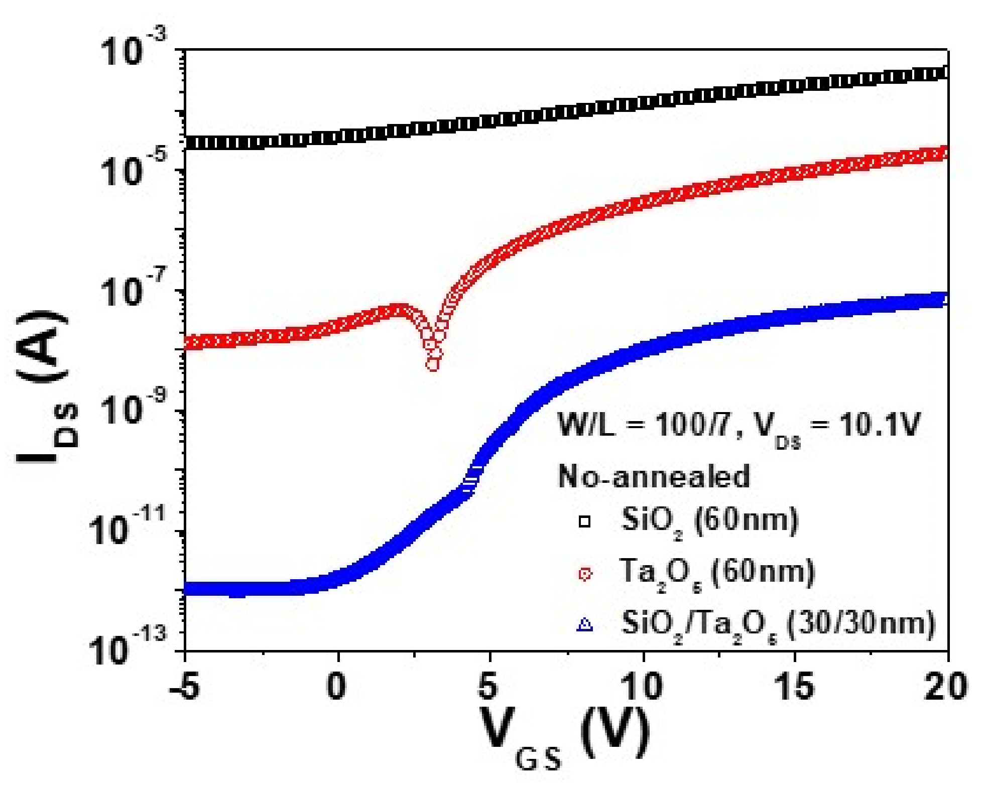
Figure 5 shows the electrical characteristics before heat treatment of a-IGZO transistor to which the gate insulating film SiO2 (60 nm), Ta2O5 (60 nm), and SiO2/Ta2O5 (30 nm/30 nm) are applied.

Figure 5.
Transfer characteristics of a-IGZO transistors according to the gate insulating (SiO2 (60 nm), Ta2O5 (60 nm), and SiO2/Ta2O5 (30 nm/30 nm)) films. The device is not annealed.
In the case of a SiO2 (60 nm) and Ta2O5 (60 nm) single gate insulating layer, the driving characteristics of the transistor are not exhibited. However, in the case of a device to which a double structure SiO2/Ta2O5 (30 nm/30 nm) is applied, the driving characteristics are visible; but the characteristics are deteriorated.
Figure 6 specifies the electrical characteristics of the Ta2O5, SiO2/Ta2O5 TFT, and SiO2 TFT devices. In the case of Figure 6a,b, compared to the SiO2 TFT device in (c), the on-current increased; indicating that the mobility was improved. In addition, when the device is turned on, the steep curvature of the SiO2/Ta2O5 TFT appears; which means that the sub-threshold slope is smaller. We believe that this significant improvement in the transfer characteristics is because of the reduction in the density of the tail states below the conduction band in a-IGZO or the increased mobility in a-IGZO.
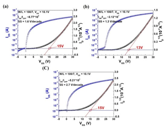
Figure 6.
Transfer curves of the (a) Ta2O5 (60 nm), (b) SiO2/Ta2O5 (30 nm/30 nm), and (c) SiO2/a-IGZO TFTs. Heat treatment was carried out for 2 h in an oxygen atmosphere at 300 °C.
We confirmed that post heat treatment had a significant effect on the improvement of the transfer properties of IGZO TFTs. In the a-IGZO thin film transistor, problems such as defects in the thin film and contact resistance between metal channels must be solved. In particular, since carrier movement in semiconductor materials greatly affects device performance, removal of defects through additional heat treatment is essential in oxide semiconductor devices [12]. In addition, the electrical contact between the channel and the source/drain in transistor fabrication is also an important factor in determining the electrical performance of the device [13]. It is possible to significantly reduce the switching speed of the transistor device. In order to improve this phenomenon, an additional heat treatment process is required.
The channel mobility and threshold voltage were calculated by linearly fitting the square root of the drain to source current (ID) vs. gate voltage (VG) curve of the transistor operating in the saturation region.
The expression for the operation of a field-effect transistor in the saturation region is as follows:
where is the channel width, L is the channel length, is the capacitance per unit area of the gate insulator, and is the threshold voltage of the TFT.
The sub-threshold slope (SS) can be determined from Ids–Vgs curves through Equation (2):
Table 1 shows a comparison of the characteristics of Ta2O5, SiO2/Ta2O5, and SiO2 TFT devices. The mobility of the SiO2/Ta2O5 TFT device is 11.3 cm2/V·s and that of the SiO2 TFT is only 0.6 cm2/V·s; in addition, the mobility is increased by almost 19 times. The on–off current ratio of the SiO2 TFT device was 105; however, the on–off current ratio of the SiO2/Ta2O5 TFT device was 107, which increased more than 10 times. Moreover, the SS value of the SiO2 TFT device was 2.7 V/dec; however, in the case of the SiO2/Ta2O5 TFT device, it dropped to 1.6 V/dec. The reduction in SS value means a faster switching speed and greater gate control capability of the SiO2/Ta2O5 TFT device. Of course, the Ta2O5 TFT device also has superior characteristics compared to the SiO2 TFT device.

Table 1.
Transistor parameters of the Ta2O5/a-IGZO and Ta2O5/SiO2/a-IGZO TFTs.
4. Conclusions
In this study, we investigated SiO2 and Ta2O5 with a single structure and SiO2/Ta2O5 with a double structure for the gate insulating film to improve transistor performance. In TFTs with a dual structure SiO2/Ta2O5, characteristics such as an on/off ratio, subthreshold swing (SS), and saturation mobility (μsat) are significantly improved compared to a single structure SiO2 and Ta2O5. By applying the double-structured gate insulating film, the surface roughness was reduced to 0.385 nm through interface control of the formed thin film. In addition, TFT driving characteristics, such as the on/off ratio, SS, and μsat, were greatly improved to 2.12 × 10⁷, 1.3 V/dec, and 11.3 cm2/Vs, respectively. The improvement mechanism was reduced charge trapping density through improved surface roughness and interfacial control. Moreover, through the post heat treatment process, the contact resistance between the channel layer and the source/drain electrodes was improved. In this study, we developed a thin film high dielectric constant gate insulating film necessary for the development of a low-temperature process oxide TFT applicable to flexible substrates. The double-structured high-k gate insulating film is a promising tool that can be applied to next-generation flexible transistors.
Author Contributions
Experiments and writing, J.-W.K. and H.K.S.; formal analysis, J.-W.K.; methodology, H.K.S. and S.Y.L.; investigation, M.P. and S.Y.L.; conceptualization, M.P. and B.-K.J.; supervision, M.K.Y. and B.-K.J.; funding acquisition, M.K.Y. All the authors have read and agreed to the published version of the manuscript.
Funding
This paper was supported by the Academic Research Fund of Dr. Myung Ki (MIKE) Hong in 2020.
Conflicts of Interest
The authors declare no conflict of interest.
References
- Nomura, K.; Ohta, H.; Takagi, A.; Kamiya, T.; Hirano, M.; Hosono, H. Room-temperature fabrication of transparent flexible thin-film transistors using amorphous oxide semiconductors. Nature 2004, 432, 488–492. [Google Scholar] [CrossRef]
- Hosono, H. Ionic amorphous oxide semiconductors: Material design, carrier transport, and device application. J. Non-Cryst. Solids 2006, 352, 851–858. [Google Scholar] [CrossRef]
- Yabuta, H.; Sano, M.; Abe, K.; Aiba, T.; Den, T.; Kumomi, H.; Nomura, K.; Kamiya, T.; Hosono, H. High-mobility thin-film transistor with amorphous In Ga Zn O4 channel fabricated by room temperature rf-magnetron sputtering. Appl. Phys. Lett. 2006, 89, 112123. [Google Scholar] [CrossRef]
- Nomura, K.; Kamiya, T.; Ohta, H.; Uruga, T.; Hirano, M.; Hosono, H. Local coordination structure and electronic structure of the large electron mobility amorphous oxide semiconductor In-Ga-Zn-O: Experiment and ab initio calculations. Phys. Rev. B 2007, 75, 035212. [Google Scholar] [CrossRef]
- Sheng, J.; Hong, T.; Lee, H.; Kim, K.; Sasase, M.; Kim, J.; Hosono, H.; Park, J. Amorphous IGZO TFT with High Mobility of ~70 cm2/(V s) via Vertical Dimension Control Using PEALD. ACS Appl. Mater. Interfaces 2019, 11, 40300–40309. [Google Scholar] [CrossRef]
- Lee, J.; Kim, D.; Yang, D.; Hong, S.; Yoon, K.; Hong, P.; Jeong, C.; Park, H.; Kim, S.Y.; Lim, S.K. 42.2: World’s Largest (15-inch) XGA AMLCD Panel Using IGZO Oxide TFT. SID Symp. Dig. Tech. Pap. 2008, 39, 625–628. [Google Scholar] [CrossRef]
- Hayashi, R.; Sato, A.; Ofuji, M.; Abe, K.; Yabuta, H.; Sano, M.; Kumomi, H.; Nomura, K.; Kamiya, T.; Hirano, M. 42.1: Invited Paper: Improved Amorphous In-Ga-Zn-O TFTs. SID Symp. Dig. Tech. Pap. 2008, 39, 621–624. [Google Scholar] [CrossRef]
- Park, S.K.; Ryu, M.; Hwang, C.; Yang, S.; Byun, C.; Lee, J.; Shin, J.; Yoon, S.M.; Chu, H.Y.; Cho, K.I. 42.3: Transparent ZnO thin film transistor for the application of high aperture ratio bottom emission AM-OLED display. SID Symp. Dig. Tech. Pap. 2008, 39, 629–632. [Google Scholar] [CrossRef]
- Takechi, K.; Nakata, M.; Eguchi, T.; Yamaguchi, H.; Kaneko, S. Temperature-dependent transfer characteristics of amorphous InGaZnO4 thin-film transistors. Jpn. J. Appl. Phys. 2009, 48, 11301. [Google Scholar] [CrossRef]
- Takechi, K.; Nakata, M.; Eguchi, T.; Yamaguchi, H.; Kaneko, S. Comparison of ultraviolet photo-field effects between hydrogenated amorphous silicon and amorphous InGaZnO4 thin-film transistors. Jpn. J. Appl. Phys. 2009, 48, 10203. [Google Scholar] [CrossRef]
- Kimura, M.; Nakanishi, T.; Nomura, K.; Kamiya, T.; Hosono, H. Trap densities in amorphous-In Ga Zn O 4 thin-film transistors. Appl. Phys. Lett. 2008, 92, 133512. [Google Scholar] [CrossRef]
- Kim, D.; Cho, W. Effects of Rapid Thermal Annealing on the Conduction of a-IGZO Films. J. Korean Inst. Electr. Electron. Mater. Eng. 2016, 29, 11–16. [Google Scholar]
- Park, J.; Kim, C.S.; Kim, Y.S.; Park, Y.C.; Park, H.J.; Bae, B.; Park, J.; Kim, H. The effect of ITO and Mo electrodes on the properties and stability of In-Ga-Zn-O thin film transistors. J. Electroceram. 2016, 36, 129–134. [Google Scholar] [CrossRef]
- Kong, H.; Cho, K.; Lee, H.; Lee, S.; Lim, J.; Kim, S. Bias-stress stability of top-gate coplanar a-ITGZO TFTs with HfO2 and HfAlO gate dielectrics. Mater. Sci. Semicond. Processing 2022, 143, 106527. [Google Scholar] [CrossRef]
- Carlos, E.; Branquinho, R.; Kiazadeh, A.; Barquinha, P.; Martins, R.; Fortunato, E. UV-Mediated Photochemical Treatment for Low-Temperature Oxide-Based Thin-Film Transistors. ACS Appl. Mater. Interfaces 2016, 8, 31100–31108. [Google Scholar] [CrossRef]
- Carlos, E.; Leppäniemi, J.; Sneck, A.; Alastalo, A.; Deuermeier, J.; Branquinho, R.; Martins, R.; Fortunato, E. Printed, Highly Stable Metal Oxide Thin-Film Transistors with Ultra-Thin High-k Oxide Dielectric. Adv. Electron. Mater. 2020, 6, 1901071. [Google Scholar] [CrossRef]
- Dong, C.; Liu, G.; Zhang, Y.; Feng, G.; Zhou, Y. Double-stacked gate insulators SiOx/TaOx for flexible amorphous InGaZnO thin film transistors. Mater. Sci. Semicond. Processing 2019, 96, 99–103. [Google Scholar] [CrossRef]
- Beom, K.; Yang, P.; Park, D.; Kim, H.J.; Lee, H.H.; Kang, C.J.; Yoon, T. Single- and double-gate synaptic transistor with TaOx gate insulator and IGZO channel layer. Nanotechnology 2018, 30, 025203. [Google Scholar] [CrossRef]
- Jauhari, I.M.; Bak, Y.G.; Noviyana, I.; Putri, M.A.; Lee, J.A.; Heo, Y.W.; Lee, H.Y. Electrical properties of amorphous indium zinc tin oxide thin film transistor with Y2O3 gate dielectric. J. Nanosci. Nanotechnol. 2021, 21, 1748–1753. [Google Scholar] [CrossRef]
- Choi, W.; Jeon, W.; Park, J. Nanoscale surface engineering of a high-k ZrO2/SiO2 gate insulator for a high performance ITZO TFT via plasma-enhanced atomic layer deposition. J. Mater. Chem. C 2020, 8, 13342–13348. [Google Scholar] [CrossRef]
- DiStefano, T.H.; Eastman, D.E. The band edge of amorphous SiO2 by photoinjection and photoconductivity measurements. Solid State Commun. 1971, 9, 2259–2261. [Google Scholar] [CrossRef]
- Green, M.L.; Sorsch, T.W.; Timp, G.L.; Muller, D.A.; Weir, B.E.; Silverman, P.J.; Moccio, S.V.; Kim, Y.O. Understanding the limits of ultrathin SiO2 and Si O N gate dielectrics for sub-50 nm CMOS. Microelectron. Eng. 1999, 48, 25–30. [Google Scholar] [CrossRef]
- Martins, J.; Kiazadeh, A.; Pinto, J.V.; Rovisco, A.; Goncalves, T.; Deuermeier, J.; Alves, E.; Martins, R.; Fortunato, E.; Barquinha, P. Ta2O5/SiO2 Multicomponent Dielectrics for Amorphous Oxide TFTs. Electron. Mater. 2021, 2, 1–16. [Google Scholar] [CrossRef]
- Hubbard, K.J.; Schlom, D.G. Thermodynamic stability of binary oxides in contact with silicon. J. Mater. Res. 1996, 11, 2757–2776. [Google Scholar] [CrossRef]
- Billman, C.A.; Tan, P.H.; Hubbard, K.J.; Schlom, D.G. Alternate gate oxides for silicon MOSFETs using high-K dielectrics. MRS Online Proc. Libr. 1999, 567, 409–414. [Google Scholar] [CrossRef]
- Wang, L.; Yoon, M.; Lu, G.; Yang, Y.; Facchetti, A.; Marks, T.J. High-performance transparent inorganic–organic hybrid thin-film n-type transistors. Nat. Mater. 2006, 5, 893–900. [Google Scholar] [CrossRef] [PubMed]
- Noh, S.H.; Choi, W.; Oh, M.S.; Hwang, D.K.; Lee, K.; Im, S. ZnO-based nonvolatile memory thin-film transistors with polymer dielectric/ferroelectric double gate insulators. Appl. Phys. Lett. 2007, 90, 253504. [Google Scholar] [CrossRef]
- Sasa, S.; Ozaki, M.; Koike, K.; Yano, M.; Inoue, M. High-performance Zn O∕Zn Mg O field-effect transistors using a hetero-metal-insulator-semiconductor structure. Appl. Phys. Lett. 2006, 89, 053502. [Google Scholar] [CrossRef]
- Lee, K.; Kim, J.H.; Im, S. Low-voltage-driven top-gate ZnO thin-film transistors with polymer/high-k oxide double-layer dielectric. Appl. Phys. Lett. 2006, 89, 133507. [Google Scholar] [CrossRef]
- Oh, M.S.; Hwang, D.K.; Kimoon, L.; Im, S. Low voltage complementary thin-film transistor inverters with pentacene-ZnO hybrid channels on AlO𝑥 dielectric. Appl. Phys. Lett. 2007, 90, 173511. [Google Scholar] [CrossRef]
- Dhananjay; Krupanidhi, S.B. Low threshold voltage ZnO thin film transistor with a Zn0.7Mg0.3O gate dielectric for transparent electronics. J. Appl. Phys. 2007, 101, 123717. [Google Scholar] [CrossRef]
- De Souza, M.M.; Jejurikar, S.; Adhi, K.P. Impact of aluminum nitride as an insulator on the performance of zinc oxide thin film transistors. Appl. Phys. Lett. 2008, 92, 093509. [Google Scholar] [CrossRef]
- Zhang, L.; Li, J.; Zhang, X.W.; Jiang, X.Y.; Zhang, Z.L. High-performance ZnO thin film transistors with sputtering SiO2/Ta2O5/SiO2 multilayer gate dielectric. Thin Solid Films 2010, 518, 6130–6133. [Google Scholar] [CrossRef]
- Carlos, E.; Branquinho, R.; Kiazadeh, A.; Martins, J.; Barquinha, P.; Martins, R.; Fortunato, E. Boosting Electrical Performance of High-k Nanomultilayer Dielectrics and Electronic Devices by Combining Solution Combustion Synthesis and UV Irradiation. ACS Appl. Mater. Interfaces 2017, 9, 40428–40437. [Google Scholar] [CrossRef] [PubMed]
- Shimura, Y.; Nomura, K.; Yanagi, H.; Kamiya, T.; Hirano, M.; Hosono, H. Specific contact resistances between amorphous oxide semiconductor In-Ga-Zn-O and metallic electrodes. Thin Solid Films 2008, 516, 5899–5902. [Google Scholar] [CrossRef]
- Verlaak, S.; Arkhipov, V.; Heremans, P. Modeling of transport in polycrystalline organic semiconductor films. Appl. Phys. Lett. 2003, 82, 745–747. [Google Scholar] [CrossRef]
- Völkel, A.R.; Street, R.A.; Knipp, D. Carrier transport and density of state distributions in pentacene transistors. Phys. Rev. B 2002, 66, 195336. [Google Scholar] [CrossRef]
- Valletta, A.; Mariucci, L.; Fortunato, G.; Brotherton, S.D. Surface-scattering effects in polycrystalline silicon thin-film transistors. Appl. Phys. Lett. 2003, 82, 3119–3121. [Google Scholar] [CrossRef]

Publisher’s Note: MDPI stays neutral with regard to jurisdictional claims in published maps and institutional affiliations. |
© 2022 by the authors. Licensee MDPI, Basel, Switzerland. This article is an open access article distributed under the terms and conditions of the Creative Commons Attribution (CC BY) license (https://creativecommons.org/licenses/by/4.0/).