Abstract
Sn–Bi alloys are desirable candidates for soldering components on printed circuit boards (PCBs) because of their low melting point and reduced cost. While certain tin–bismuth solders are well characterized many new alloys in this family have been developed which need proper characterization. The following study looks at the behavior of four different Sn–Bi alloys—traditional 42Sn58Bi and 42Sn57Bi1Ag and two new tin–bismuth alloys—in solder paste during the reflow soldering process. Each alloy was processed using different reflow profiles that had varying times above liquidus (TALs) and peak temperatures. The PCBs were then analyzed to see how the processing variables influenced wetting, voiding, microstructure, intermetallic layer composition, and thickness. After analysis, the PCBs were then subjected to thermal cycling experiments to see how reflow profile impacted microstructure evolution. The results demonstrated that reflow profile affects properties such as metal wetting and voiding. It does not however, greatly impact key metallurgical properties such as intermetallic layer thickness.
1. Introduction
1.1. Surface Mount Technology
Solder alloys play a pivotal role in surface mount technology (SMT). When used in materials such as solder paste, they are vital for the assembly of components on printed circuit boards (PCBs) through processes such as reflow soldering [1]. Two key variables in reflow soldering are peak reflow temperature and the time above liquidus (TAL) [2]. During the reflow process, solder alloys are exposed to peak temperatures that extend 25–50 °C above their melting point to ensure that components are properly fused to the PCB [3]. The exact temperature at which they are processed as well as how long they are kept at this temperature, TAL, are known to affect the reflowed solder joint [4].
1.2. The Transition to Lead-Free Solders
The introduction of the Restriction of Hazardous Substances (RoHS) in 2006, which banned the use of lead in alloys used for reflow soldering, presented numerous challenges for the surface mount technology (SMT) industry [5,6]. Tin–lead alloys had previously been the industry standard because of their many desirable properties including low melting point [7], low surface tension [8] and good mechanical reliability [9]. Initially, SAC-based (tin–silver–copper) alloys replaced their leaded counterparts [10].
While SAC-based alloys have desirable mechanical properties, there are other issues associated with their use [11]. Notably, SAC305 (96.5% tin, 3% silver and 0.5% copper), the benchmark alloy for the industry, has a high melting point (217–219 °C) [12]. This poses a challenge for the SMT assembly process for numerous reasons. Firstly, with the ongoing miniaturization trend, components continue to become thinner and more susceptible to thermal stress [13]. This increased thermal stress is known to cause component package warping and is common with SAC-based systems [14]. Furthermore, given its high melting point, temperatures ranging from 240–270 °C are needed to properly process these alloys during reflow. From an environmental perspective, this requires the consumption of large amounts of energy producing excessive carbon dioxide emissions [15]. Lastly, from an economic point of view, higher energy costs are associated with greater energy consumption [16].
1.3. Tin–Bismuth Solders
Tin–bismuth solders are viewed as a viable alternative to SAC-based alloys [17]. They were initially considered as a replacement for tin–lead alloys when RoHS was introduced in 2006 but were disregarded since they form a low melting point intermetallic compound (IMC) with lead, Sn16Pb32Bi52 (melting point = 96 °C), which could compromise reliability of a reflowed solder joint [18]. It was thought that in the nascent period of the transition to lead-free materials, lead would still be found in components and substrate materials, so SAC-based alloys were selected over tin–bismuth [19].
Now that lead has been completely phased out of the supply chain, the concerns over the low melting point IMC are no longer relevant. This has made tin–bismuth solders an attractive candidate for SMT assembly once again. The main alloy in this family, 42Sn58Bi, has a eutectic melting point of 138 °C, which is well below that of tin–lead alloys [20]. The melting point would provide a substantial advantage over SAC-based alloys due to the lower peak reflow temperatures required for the process. In turn, this is expected to reduce the energy consumption of the SMT assembly process and result in higher process yields because of reduced package warping [21].
The principal drawback of tin–bismuth alloys is their brittle nature because of bismuth’s natural characteristics [15]. Bismuth can form a solid solution with tin up to 4% in concentration [22]. Once this concentration has been passed, bismuth precipitates out to form lamellae-like structures which compromise the ductility of the solder [23]. Adding certain dopants such as silver [24], cobalt [25] and nickel [26] has been shown to improve the mechanical properties of tin–bismuth solders via several mechanisms such as grain refinement [27] and precipitate strengthening [28].
1.4. How Do Processing Conditions Affect Properties of Reflowed Tin–Bismuth Solders?
It is well known that the processing temperatures used in reflow soldering greatly influence the properties of the finished solder joint on the PCB [29]. The effect of peak reflow temperature and time above liquidus has been studied in SAC [2] and tin–lead [30] based systems. While much work has been done to study the effect of reflow profile on conventional tin–bismuth and tin–bismuth silver alloys many new tin–bismuth alloys containing dopants such as copper [31], nickel [32], antimony [26] and nanomaterials [33] have been developed which are not as well-characterized. In this study, four tin–bismuth solder pastes will be studied to properly understand how varying peak temperature and time above liquidus during reflow influence properties such as IMC formation, metal wetting, and voiding on a finished PCB. Voids, caused by the Kirkendall effect or flux medium volatiles getting trapped in the cooled solder, are known to cause issues with solder joint reliability [34]. Current IPC standards dictate that voiding levels be less than 25% of the solder joint. Two of the alloys studied are eutectic 42Sn58Bi and 42Sn57Bi1Ag. The remaining alloys being examined are two proprietary alloys which have been doped with microalloying elements such as Sb and Cu to improve ductility. While 42Sn58Bi and 42Sn57Bi1Ag have been extensively studied the other two alloys have not and little is known about how these alloys behave during typical SMT process windows.
Moreover, the link between peak reflow temperature, TAL and the mechanical properties of certain categories of tin–bismuth solders is not well understood. Following the characterization experiments of the metallurgical properties of the reflowed PCB, the alloys were subjected to thermal cycling experiments to see if varying peak temperature and TAL creates structural changes that would compromise mechanical reliability of the solder joint. They were then compared to PCBs reflowed with 42Sn58Bi and 42Sn57Bi1Ag whose metallurgical properties are well understood.
2. Materials and Methods
2.1. Materials
Solder pastes were made by blending metal powders with a commercially available flux medium in a concentration of 88.5% by weight metal and 11.5% by weight flux medium. The tin-bismuth alloys studied are listed in Table 1. All solder pastes were purchased directly from the manufacturer. To ensure that there were no variations in data due to flux medium chemistry, the same commercially available flux medium formulation was used for all the pastes tested. The flux medium is classified as ROL1 per IPC J-STD-004B and is designed specifically for use with low temperature alloys. The flux medium is a conventional no clean flux which consists of the typical ingredients such as rosins, weak organic acids, and amines. It has a melting point of 92 °C.

Table 1.
Tin–bismuth alloys under investigation.
2.2. Printing Experiments
Solder paste was printed on copper boards with organic solderability preservatives (Cu-OSP) using a 100 µm thick laser cut stainless steel stencil. The boards were used as received from the manufacturer. Following paste deposition, quad flat no leads packages (QFNs) with a SAC305 metallization were applied to the boards. The assembly was then passed through a 10 zone reflow oven. A total of 5 different reflow profiles were studied, each with varying TALs and peak temperature (Table 2). All were a ramp to spike (RTS) profile.
Table 2.
RTS reflow profiles studied in this work.
Following reflow, the boards were inspected optically to examine their final appearance and key characteristics such as metal wetting and solder joint appearance. The boards were also analyzed via 2D X-ray to determine the voiding levels in quad flat no leads (QFN) packages.
2.3. Analysis of the Metallurgical Properties of the Reflowed Solder Joints
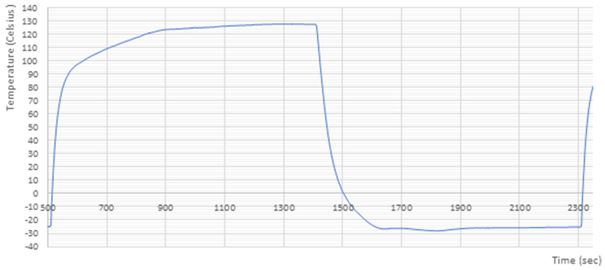
Samples were cut out of the PCB and were divided into five groups of 10 samples. Following this, the PCBs were subject to thermal cycling for a total of 1000 cycles in a thermal shock test cabinet TSS-70/66 (CTS GmbH, Hechingen, Germany). The temperature in the cold chamber was set to −25 °C, the temperature in the hot chamber was +125 °C and the hot-cold cycle took 30 min. The ramp rate was +0.75 °C/min and −0.3 °C/min respectively. Figure 1 represents the temperature profile studied for one cycle. The PCBs were incubated for 15 min at each temperature. Cycling was paused after 250, 500, 750 and 1000 cycles to collect a cross-section and analyze the evolution of the microstructure and intermetallic layer.
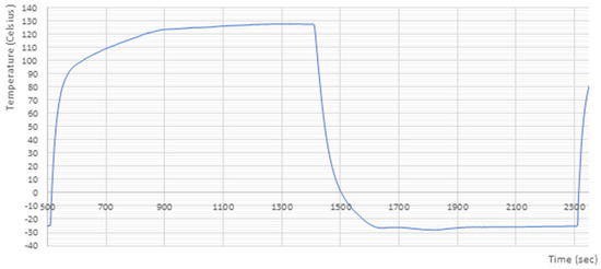
Figure 1.
Thermal cycling profile applied to the cut-out samples.
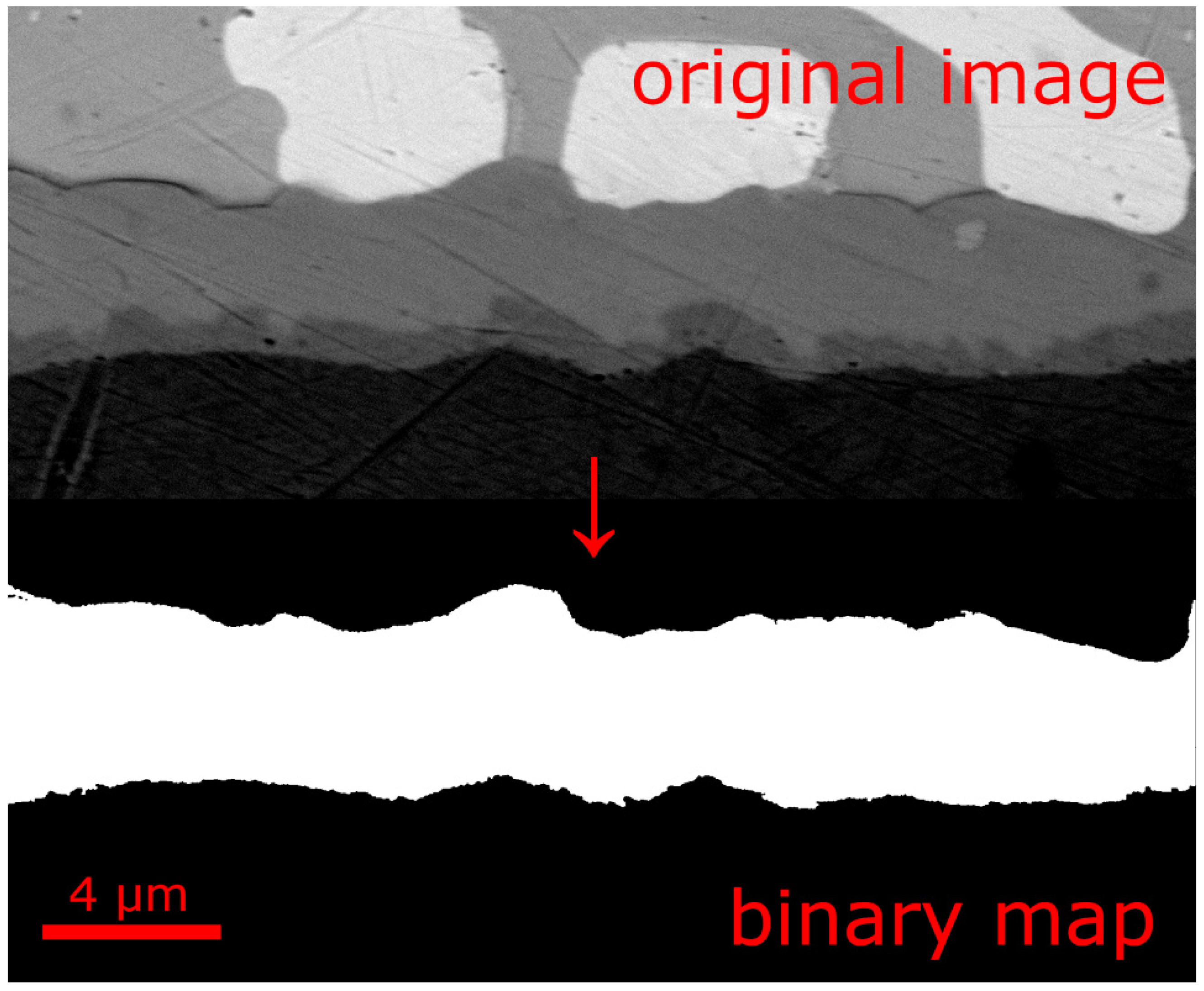
The cross sections collected at 0, 250, 500, 750 and 1000 thermal cycles were analyzed via scanning electron microscopy (SEM) and energy dispersive X-ray spectroscopy (EDX). Electron microscope (Phenom pro X, Thermo Fisher Scientific, Waltham, MA, USA) at the 10,000× magnification and at an accelerating voltage of 15 kV was used for the analysis. The IMC layer thickness evaluation was done using binary images created with NIS Elements software (Windows Version, Nikon Metrology NV, Tring, UK) from original SEM images (Figure 2). The selection of the IMC layer was based on brightness difference and was created semi automatically. The calibrated binary images were then processed with a custom written script that sliced the image vertically and calculated the number of white pixels representing the IMC layer in each “slice”. The average thickness and standard deviation of the IMC layer thickness for each sample was estimated.

Figure 2.
Conversion from original scanning electron microscopy (SEM) image of intermetallic layer (IML) to a binary map.
EDX analysis on selected samples was conducted at the accelerating voltage of 15 kV to reveal the elemental composition of the intermetallic compounds in the reflowed solder joint.
3. Results
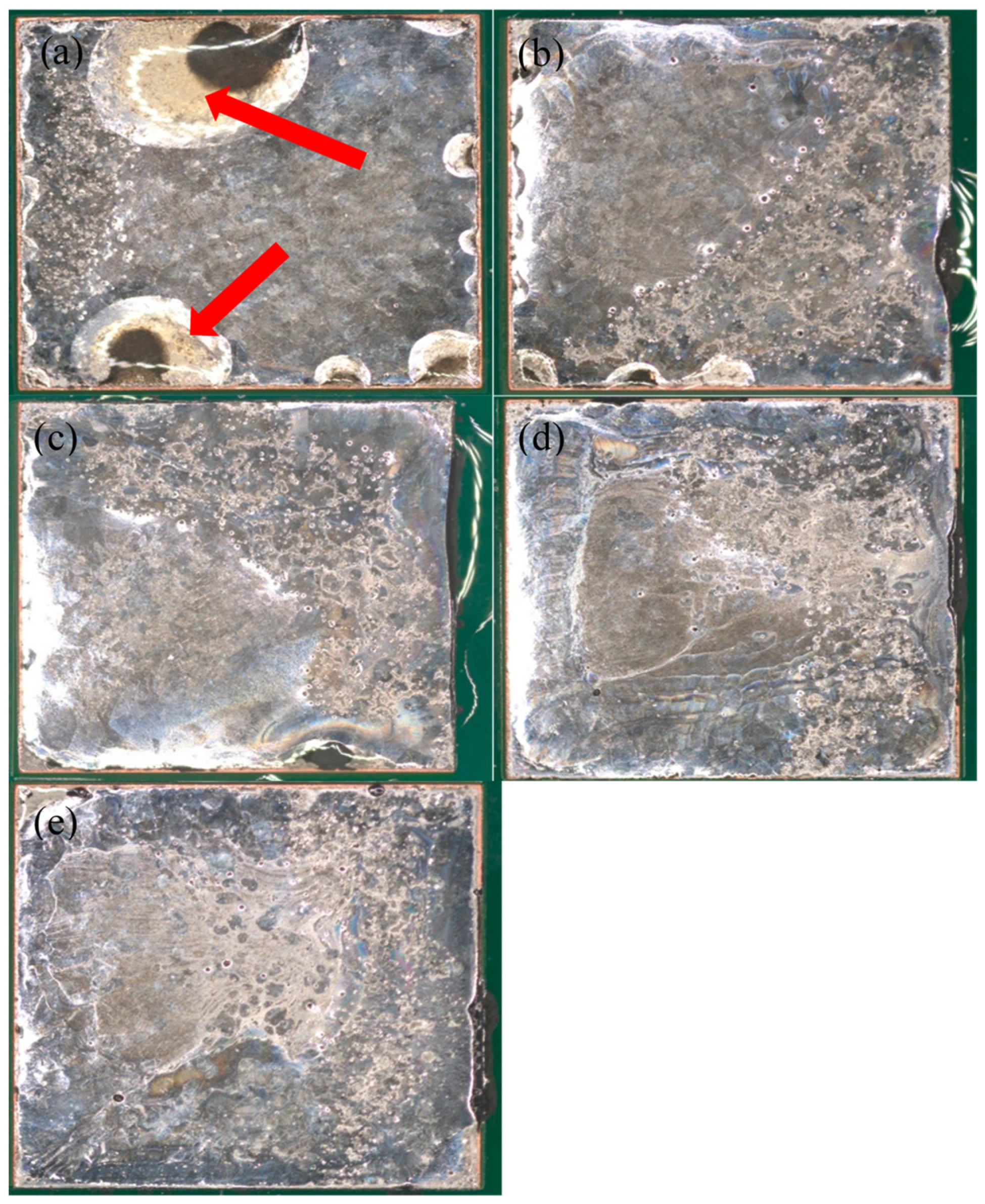
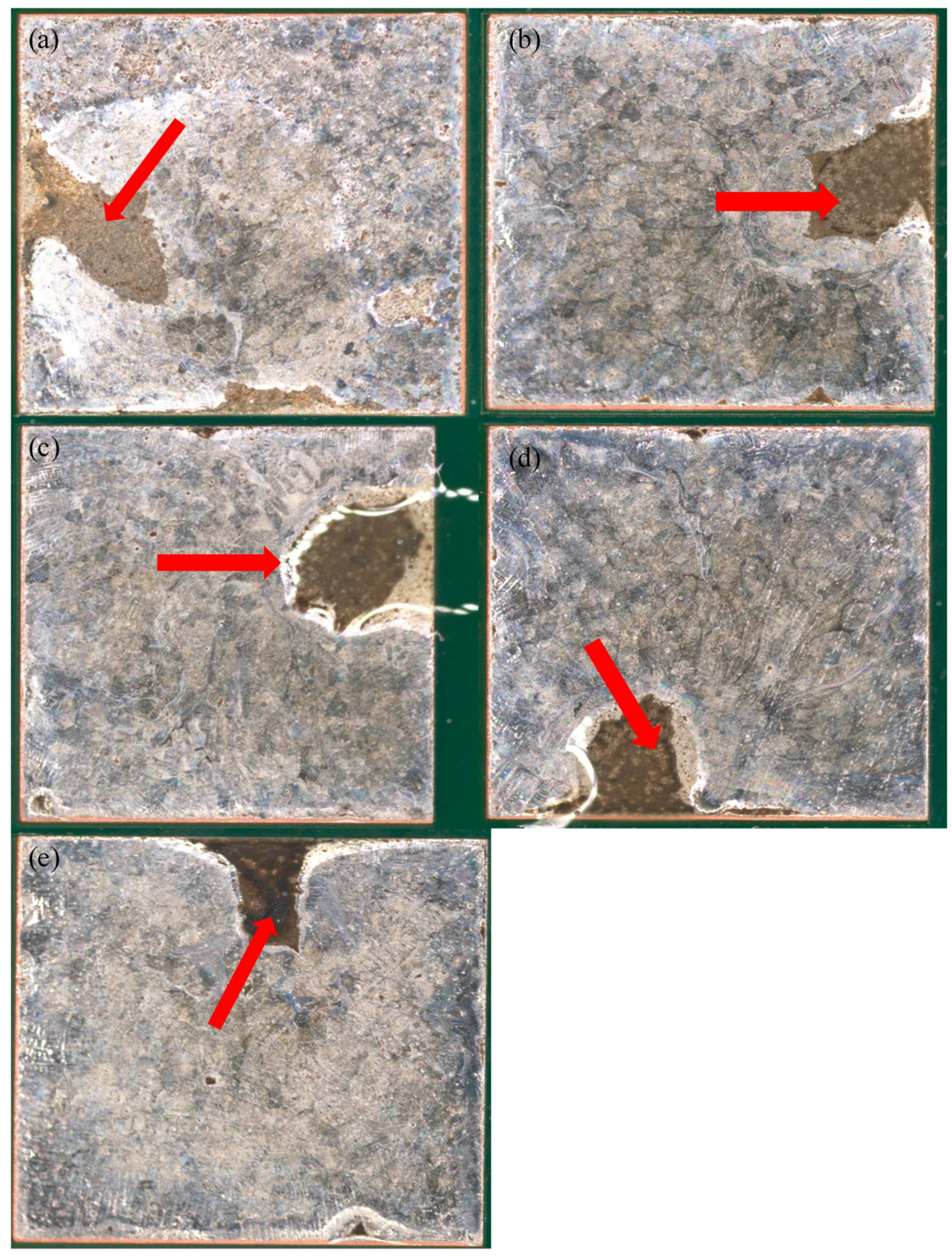
3.1. Printing Results and Wetting and Voiding Results
Boards made with Cu-OSP finish had solder paste deposited on them and were reflowed using the profiles listed in Table 2. All boards were sourced from the same lot of Cu-OSP boards to minimize differences in substrate roughness, which is known to affect metal wetting. Boards were used as received from the manufacturer, to represent what happens in a typical surface mount assembly line. Furthermore, to avoid differences in wetting due to paste volume all boards were printed using a 100 µm thick laser-cut stainless steel stencil. The paste volume was confirmed using optical solder paste inspection techniques. The %volume deposition, which compares the actual paste volume deposited to the theoretical one, for all pastes studied was found to varied from 104–107% indicating that all PCBs had nearly identical volumes of solder paste printed on them. A range of peak temperatures and TALs, which are typical of those used in the SMT industry, were selected to understand how these two variables influence the qualities of the reflowed solder joint. Short TALs and low peak temperatures are known to minimize the formation of the IMC layer between the solder and the board, however this may lead to poor soldering. Conversely, long TALs and high peak temperatures favor this reaction, but excess IMC formation can embrittle the solder joint [35]. Printed circuit boards (PCBs) were first studied optically for their wetting properties on Cu-OSP boards (Figure 3, Figure 4, Figure 5 and Figure 6) and the degree to which they spread and wet the pad was quantified (Table 3). Areas with significant amounts of non-wetting are highlighted in red. Wetting was expressed as % area of the pad covered by solder. The pad selected for the analysis measures 40.3225 mm2 in area.

Figure 3.
Optical images of 42Sn58Bi reflowed with (a) a peak temperature of 165 °C and 45 s time above liquidus (TAL), (b) peak temperature of 165 °C and 90 s TAL, (c) peak temperature of 177 °C and 45 s TAL, (d) peak temperature of 177 °C and 90 s TAL and (e) peak temperature of 190 °C and 90 s TAL. Red arrows indicate areas where the alloy does not cover the copper substrate.

Figure 4.
Optical images of 42Sn57Bi1Ag reflowed with (a) a peak temperature of 165 °C and 45 s TAL, (b) peak temperature of 165 °C and 90 s TAL, (c) peak temperature of 177 °C and 45 s TAL, (d) peak temperature of 177 °C and 90 s TAL and (e) peak temperature of 190 °C and 90 s TAL. Red arrows indicate areas where the alloy does not cover the copper substrate.
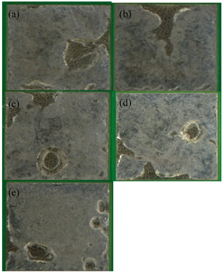
Figure 5.
Optical images of LT 47 reflowed with (a) a peak temperature of 165 °C and 45 s TAL, (b) peak temperature of 165 °C and 90 s TAL, (c) peak temperature of 177 °C and 45 s TAL, (d) peak temperature of 177 °C and 90 s TAL and (e) peak temperature of 190 °C and 90 s TAL.
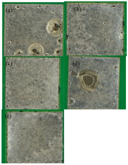
Figure 6.
Optical images of LT 51 reflowed with (a) a peak temperature of 165 °C and 45 s TAL, (b) peak temperature of 165 °C and 90 s TAL, (c) peak temperature of 177 °C and 45 s TAL, (d) peak temperature of 177 °C and 90 s TAL and (e) peak temperature of 190 °C and 90 s TAL.
Table 3.
Examination of solder coverage of copper pad as a function of reflow profiles.
Examination of the wetting reveals two key trends: both longer TALs and high peak temperatures favor metal wetting. This is especially evident in the case of 42Sn58Bi (Figure 3) At the lowest peak temperature and TAL, the solder fails to cover the copper pad completely (Figure 3a) and is confirmed by the data in Table 3 where only 64.75% of the pad is covered by the solder alloy. As both variables are raised the solder achieves better coverage on the pad and has a shinier appearance. A similar explanation applies to 42Sn57Bi1Ag and to an extent to LT 47 though it is much less pronounced (Figure 4 and Figure 5). In the case of these two solder pastes there is greater pad coverage at the mildest reflow settings when compared to 42Sn58Bi (Table 3) so the improvements in wetting as a function of peak temperature and TAL are modest. LT 51 (Figure 6) shows consistently high levels of pad coverage (Table 3) at all reflow conditions studied suggesting that it has the best performing solder paste examined in this study. While pad coverage does improve as TAL and peak temperature increase, both alloys seem to have a grainy and dull appearance. The one exception to this general trend is LT 51 which shows superior pad coverage even under mild reflow conditions suggesting that this alloy works under a greater range of reflow conditions compared to the others studied.
The wetting trends are likely a result of the interactions between the flux medium, solder alloy and soldered surfaces. Proprietary differential scanning calorimetry (DSC) data for the solder paste indicates that the reaction between the two components is most efficient between 180 and 190 °C, therefore the wetting should be superior at the higher peak temperatures studied in this work. Furthermore, using longer TALs gives the flux medium more time to effectively remove the oxide from the molten solder which also favors wetting.
Another key observation of the wetting data is the presence of a black residue in many of the reflowed PCBs. Scanning electron microscopy (SEM) and energy dispersive X-ray spectroscopy (EDX) were conducted (Supplementary Materials, Figure S1) to identify its key components. The EDX data shows that the black residue is rich in carbon and oxygen which is not observed in parts where no residue is present. This suggests that the black residue is oxidized flux medium.
What is also interesting to note is that both 42Sn57Bi1Ag and LT 47 contained a greater quantity of black residue. The common denominator between these two alloys is the presence of silver, which is not in the other two studied. One possible explanation for this is that silver is known to behave as a catalyst for certain oxidation reactions in organic chemistry [36]. Therefore, it seems likely that the silver is catalyzing the oxidation of one of the flux medium ingredients, creating more black residue compared to the other two alloys. All pastes tested had the same metal load, 88.5% and was blended with Type 4 metal alloy spheres. The volume of flux as well as the ratio of the flux quantity to surface was kept constant through all experiments indicating that neither of these variables played a role in the quantity of black residue formed.
Lastly, it appears that lower peak temperatures and short TALs favour the formation of the black residue. As previously stated, the reaction between the flux medium, solder alloy and soldered surfaces is more efficient between temperatures of 180 to 190 °C. Therefore, it seems likely that at higher peak temperatures more flux is consumed for this reaction leaving less residue that can be oxidized.
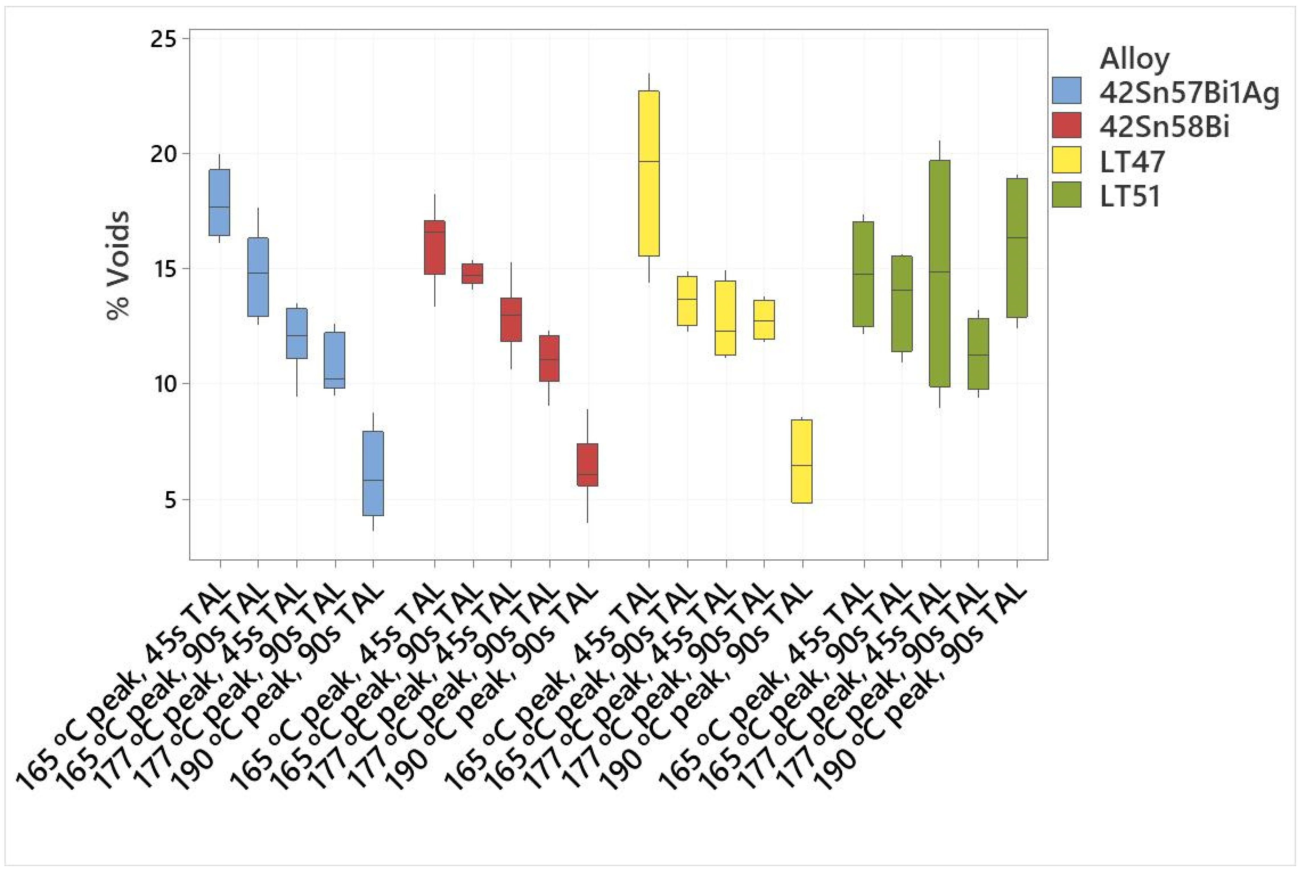
Following optical inspection of the reflowed PCBs, the solder joints were analyzed with 2D X-ray to determine the levels of voiding in quad flat no leads components (QFNs). QFNs are particularly susceptible to voiding because of the lack of standoff points in the package where volatiles from the flux medium can escape during the reflow process [37]. A boxplot representing the average levels of voiding for each component at each reflow temperature is presented in Figure 7. A typical X-ray image for each alloy can be found in the supplementary information (Supplementary Materials, Figure S2).

Figure 7.
Voiding boxplot demonstrating the average voiding levels measured in quad flat no leads (QFN) components for 42Sn58Bi, 42Sn57Bi1Ag, LT 47 and LT 51.
Examination of Figure 7 reveals that for all the alloys except for LT 51, voiding seems to decrease with increasing TAL and peak temperature. The voiding is thought to be caused by volatilization of the flux medium. In all cases, QFN voiding was well below 25% which exceeds industry standards. The observed trend is related to the reaction between the flux medium, solder alloy and soldered surfaces. As previously stated, the reaction between them is most effective between 180 and 190 °C. This would indicate that at higher peak temperatures more oxide is removed from the surface of the molten solder, lowering the surface tension and making it easier for gases to escape. A similar explanation applies for the effect of TAL. Increasing this variable allows more time for the reaction between the flux medium and molten solder to proceed. Furthermore, it provides more time for the volatiles to outgas prior to cooling of the solder joint.
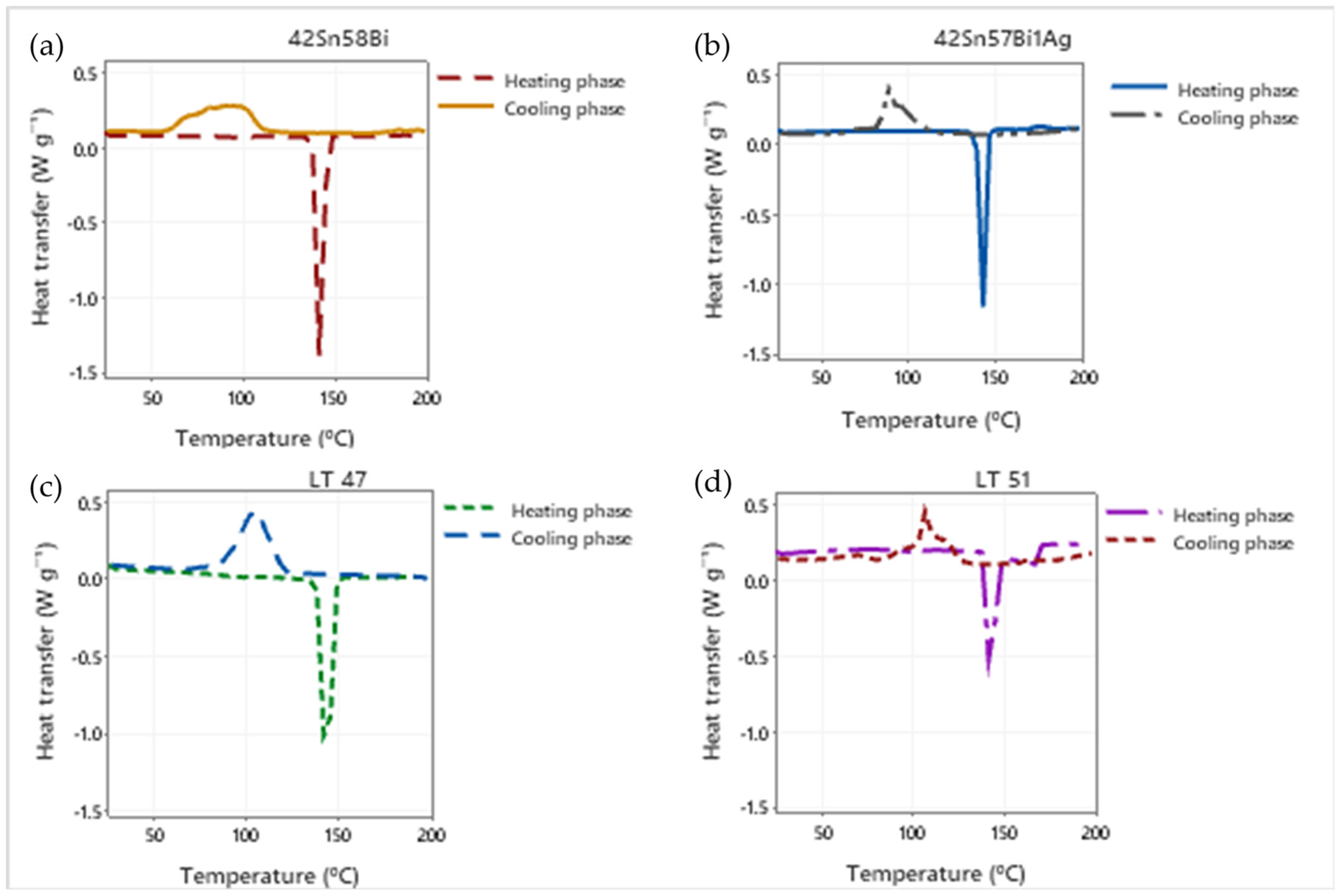
The one exception to this trend seems to be LT 51 whose voiding levels remain quite constant over the temperature range studied. The voiding in QFN components reflowed with LT 51 seems to remain constant over the range of peak temperatures and TALs studied. To understand why it behaves differently, differential scanning calorimetry (DSC) was done for powder samples for all four alloys (Figure 8). Both melting and cooling curves were collected.

Figure 8.
Differential scanning calorimetry (DSC) of for (a) 42Sn58Bi, (b) 42Sn57Bi1Ag, (c) LT 47, (d) LT 51.
Investigation of Figure 8 shows that what distinguishes LT 51 (Figure 8d) from the other alloys studied (Figure 8a–c) is the presence of a wide pasty range and a higher solidification temperature upon cooling. LT 51 displays a solidus temperature of 138 °C and a liquidus temperature of 168 °C. This is due to the present of the doping element in the alloy. When the alloy is prepared the dopant forms an intermetallic compound with Sn. LT 51 starts melting at 138 °C as is expected for a tin–bismuth alloy, however the phase change is not complete until the dopant-Sn intermetallic compound has also melted completely, thus yielding the higher pasty range. An alloy in the pasty range will be quite viscous, making it difficult for volatiles to escape the molten solder. If the alloy spends most of the reflow process at temperatures within its pasty range, the flux will have a difficult time escaping and is more likely to become entrapped in the solder joint.
Furthermore, Figure 8d reveals that LT 51 solidifies at a slightly higher temperature than the other alloys studied. While the other alloys solidify either below or around 100 °C (Figure 8a–c) LT 51 solidifies above 100 °C. This does not provide the volatiles sufficient time to escape from the solder prior to cooling, leading to a greater amount of them becoming trapped in the solder joint.
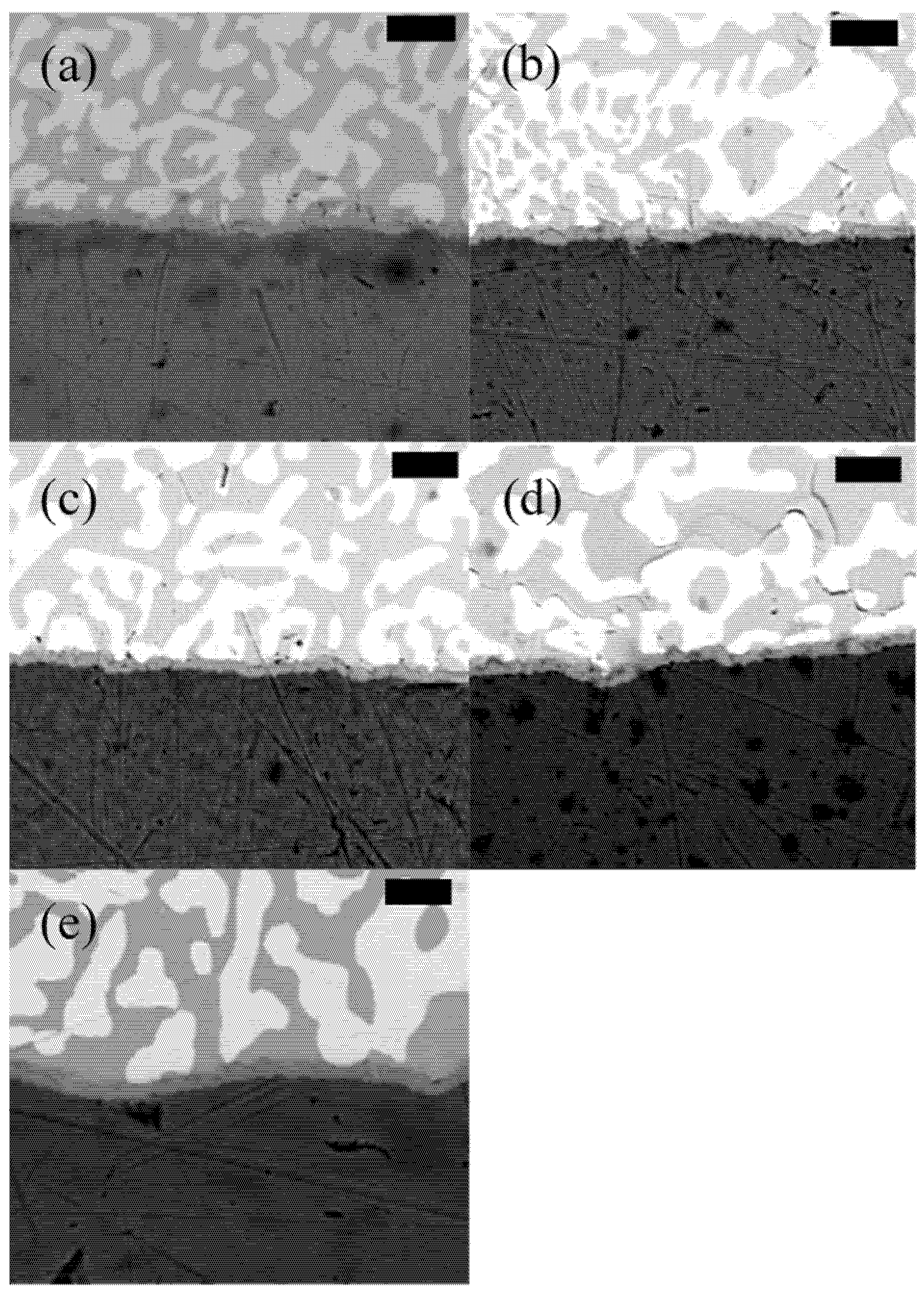
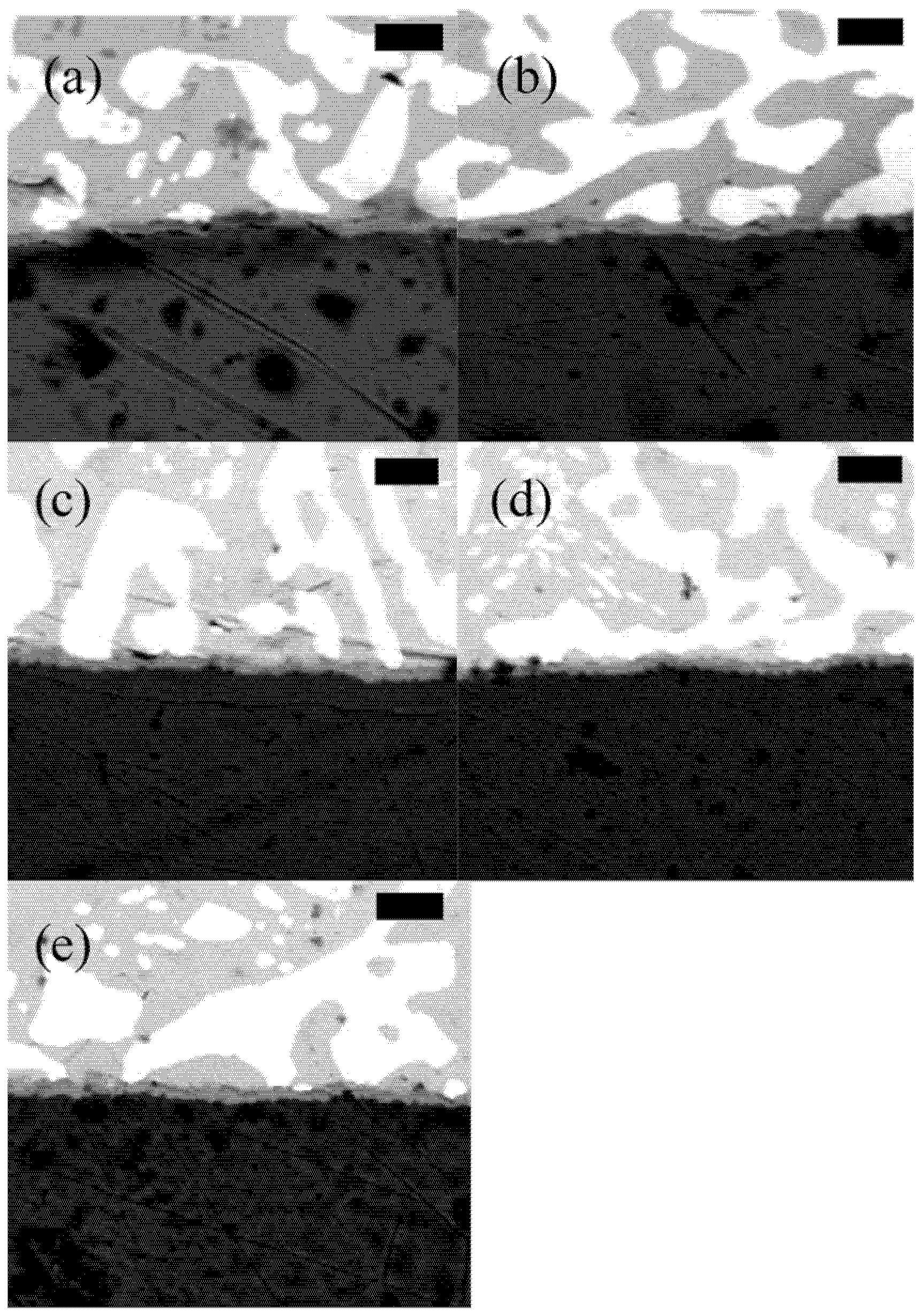
3.2. Metallurgical Analysis of the Reflowed PCB
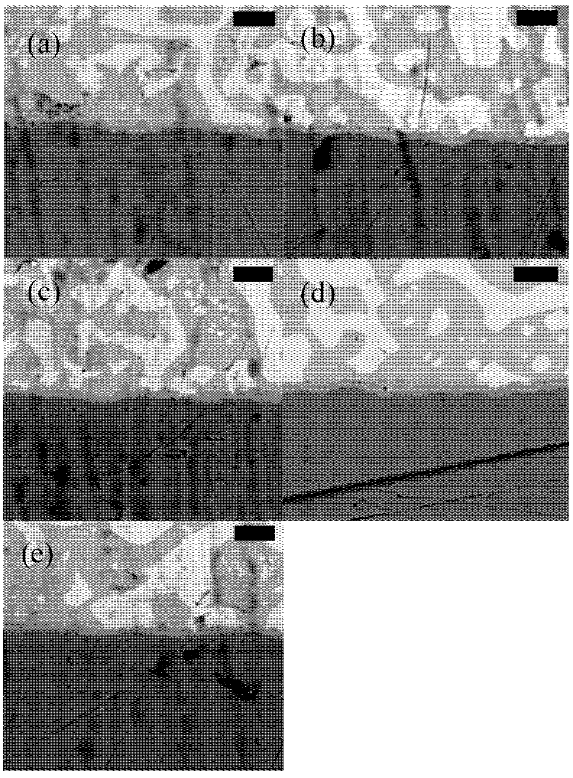
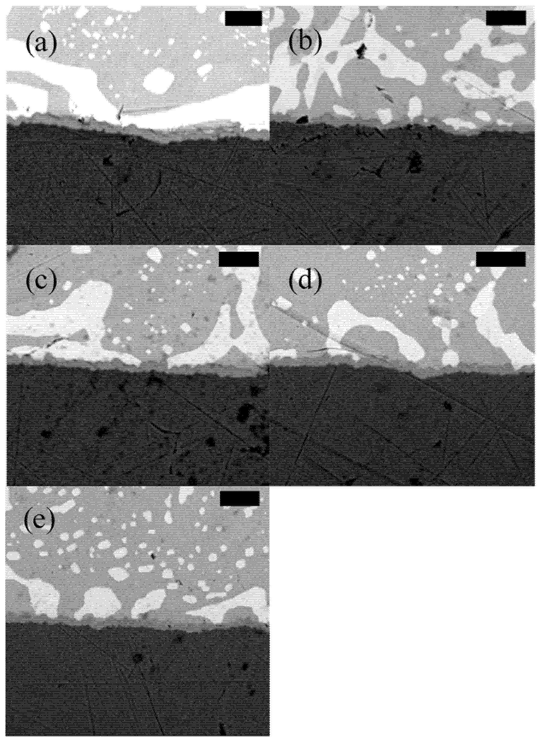
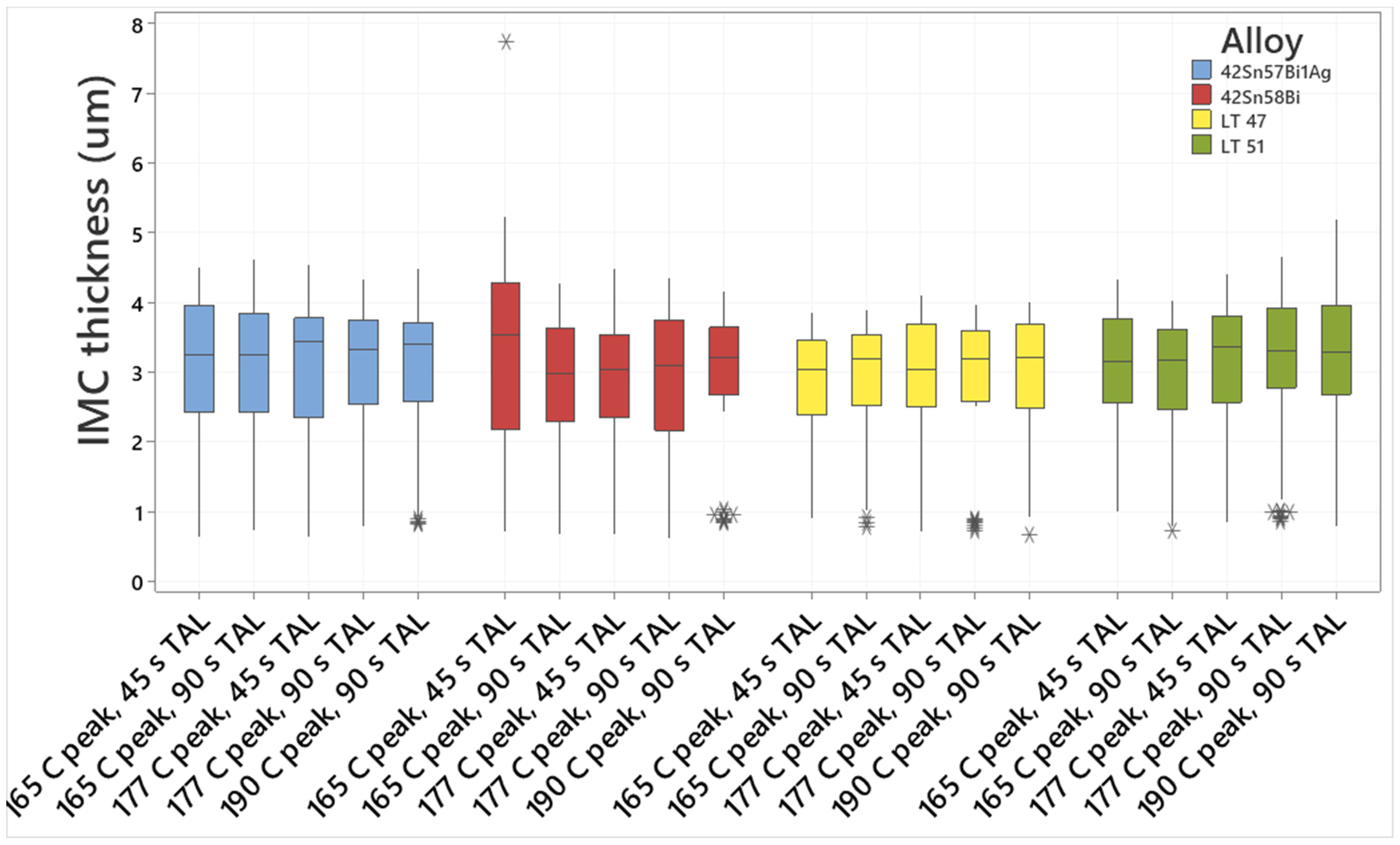
The reflowed PCBs were subsequently taken for cross-section and analysis in the SEM to study the microstructure and composition and thickness of the intermetallic (IMC) layer. A representative image for each alloy and reflow profile condition is presented in Figure 9, Figure 10, Figure 11 and Figure 12. Intermetallic layer thickness was measured by taking the average of 10 measurements for each alloy. The results are presented in a boxplot in Figure 13.
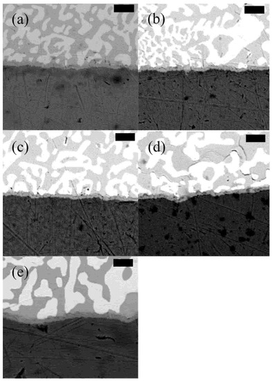
Figure 9.
SEM images of 42Sn58Bi reflowed with (a) a peak temperature of 165 °C and 45 s TAL, (b) peak temperature of 165 °C and 90 s TAL, (c) peak temperature of 177 °C and 45 s TAL, (d) peak temperature of 177 °C and 90 s TAL and (e) peak temperature of 190 °C and 90 s TAL. The scale bar is 4 µm in all images.

Figure 10.
SEM images of 42Sn57Bi1Ag reflowed with (a) a peak temperature of 165 °C and 45 s TAL, (b) peak temperature of 165 °C and 90 s TAL, (c) peak temperature of 177 °C and 45 s TAL, (d) peak temperature of 177 °C and 90 s TAL and (e) peak temperature of 190 °C and 90 s TAL. The scale bar is 4 µm in all images.

Figure 11.
SEM images of LT 47 reflowed with (a) a peak temperature of 165 °C and 45 s TAL, (b) peak temperature of 165 °C and 90 s TAL, (c) peak temperature of 177 °C and 45 s TAL, (d) peak temperature of 177 °C and 90 s TAL and (e) peak temperature of 190 °C and 90 s TAL. The scale bar is 4 µm in all images.

Figure 12.
SEM images of LT 51 reflowed with (a) a peak temperature of 165 °C and 45 s TAL, (b) peak temperature of 165 °C and 90 s TAL, (c) peak temperature of 177 °C and 45 s TAL, (d) peak temperature of 177 °C and 90 s TAL and (e) peak temperature of 190 °C and 90 s TAL. The scale bar is 4 µm in all images.

Figure 13.
Boxplot of intermetallic thickness in PCBs reflowed with Sn–Bi alloys.
Sn58Bi, 42Sn57Bi1Ag and LT 47 show a similar appearance. Both contain large lamella-like bismuth rich phases (white) and tin-rich phases (grey). While LT 51 also contains the bismuth-rich lamella structures, their size seems to be smaller compared to the other alloys. It appears that the dopants used in these this alloy form intermetallic compounds with tin which inhibit growth of the bismuth lamellae. The LT 51 solder pastes was obtained directly from the solder paste manufacturer and the alloy components were not disclosed. Closer examination of the SEM images for LT 51 reveals the presence of IMCs in the tin matrix of the reflowed solder.
All four alloys formed an intermetallic layer with the copper substrate which when analyzed by SEM and EDX (Supplementary Materials, Figure S3) was found to be Cu6Sn5 which is consistent with other reports for tin–bismuth solder alloys [34]. Examination of Figure 13. reveals that there is no clear trend in differences of the IMC layer in different alloys regardless of reflow temperature. The data does suggest that IMC layer thickness may be slightly influenced by peak temperature and TAL, however the effect is minimal. Longer TALs and higher peak temperatures do seem to favor slightly thicker IMC layers however it is not enough to compromise the reliability of the solder joint. This suggests that all four alloys are incredibly robust and can withstand a large window of reflow conditions without compromising the quality of the solder joint. This is an improvement over SAC-based systems where reflow profile has been shown to negatively impact the reflowed solder joint [30].
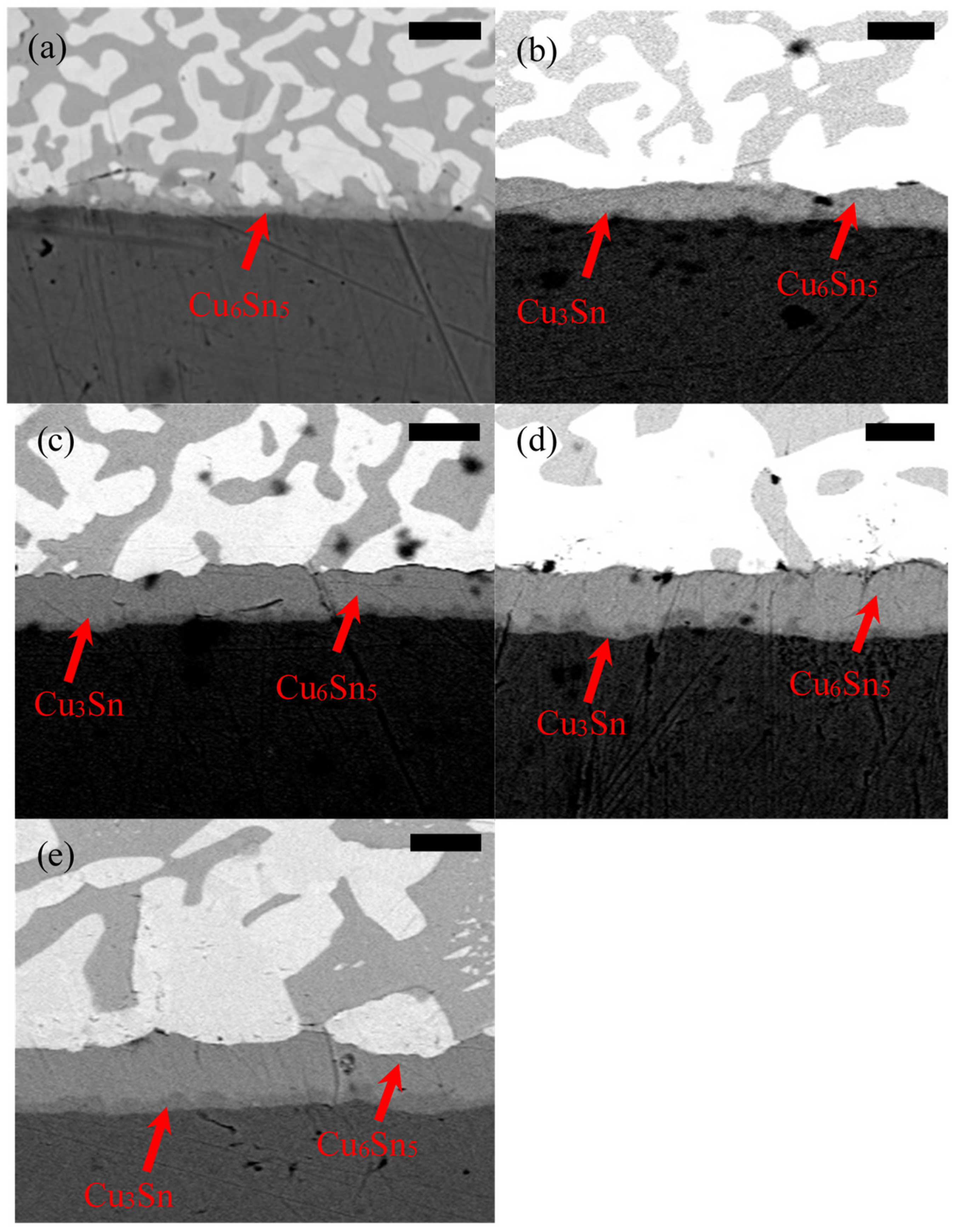
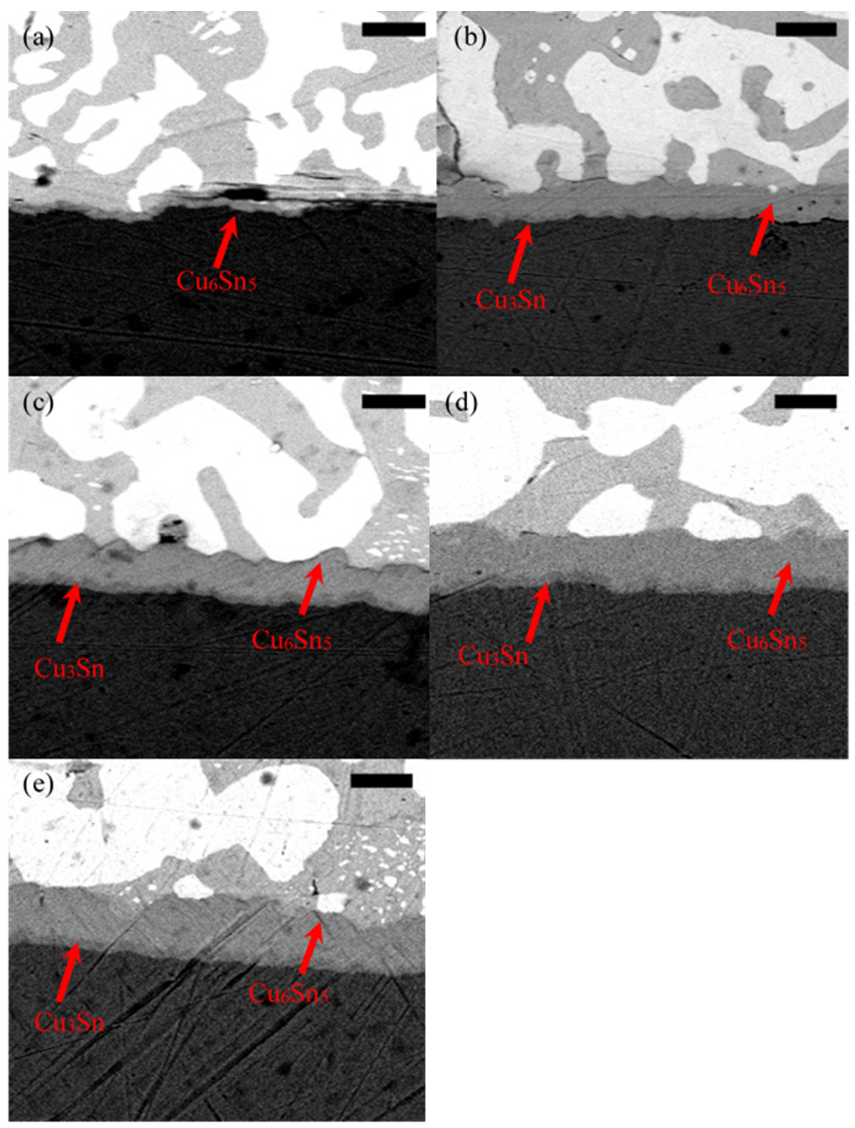
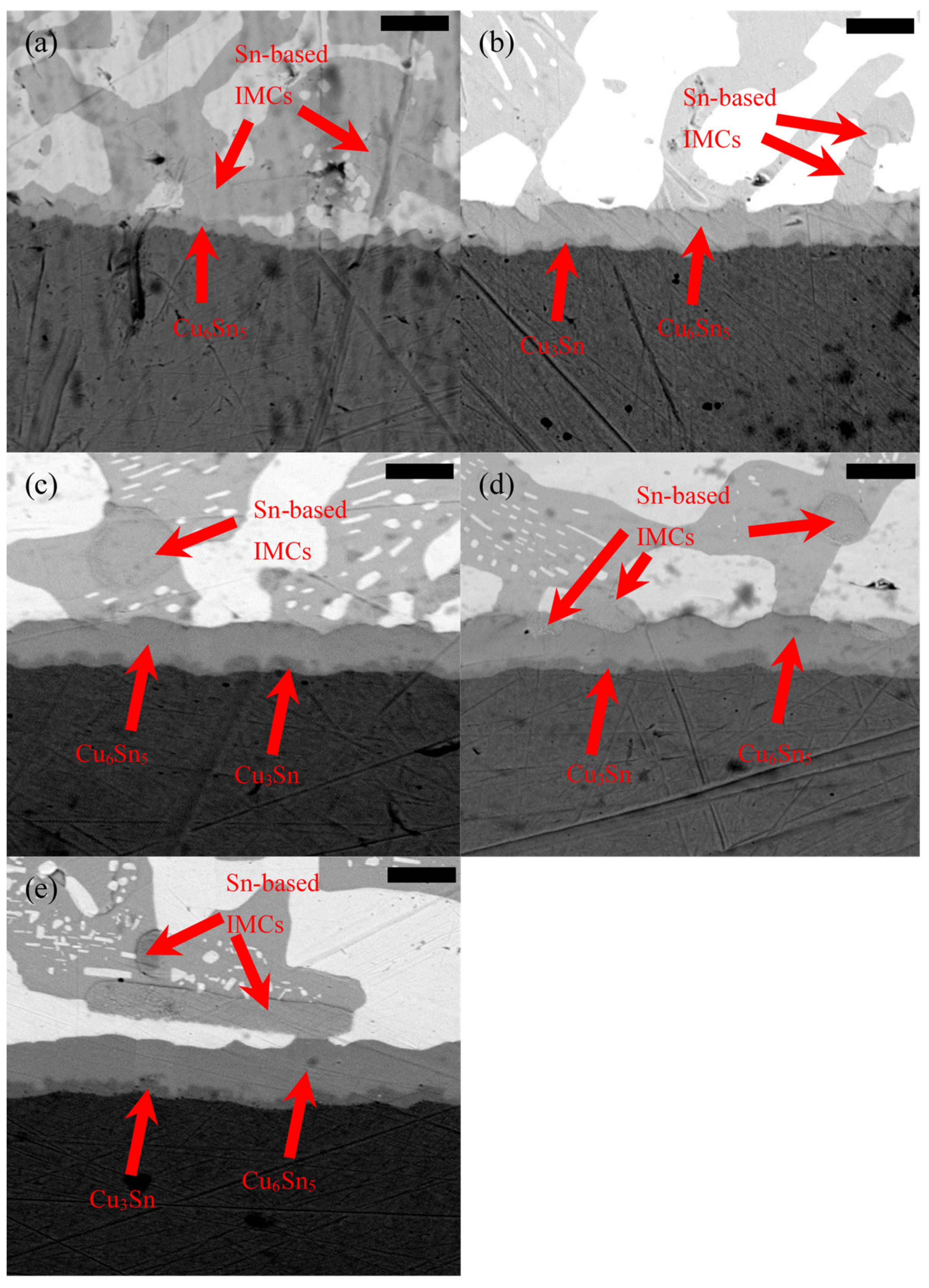
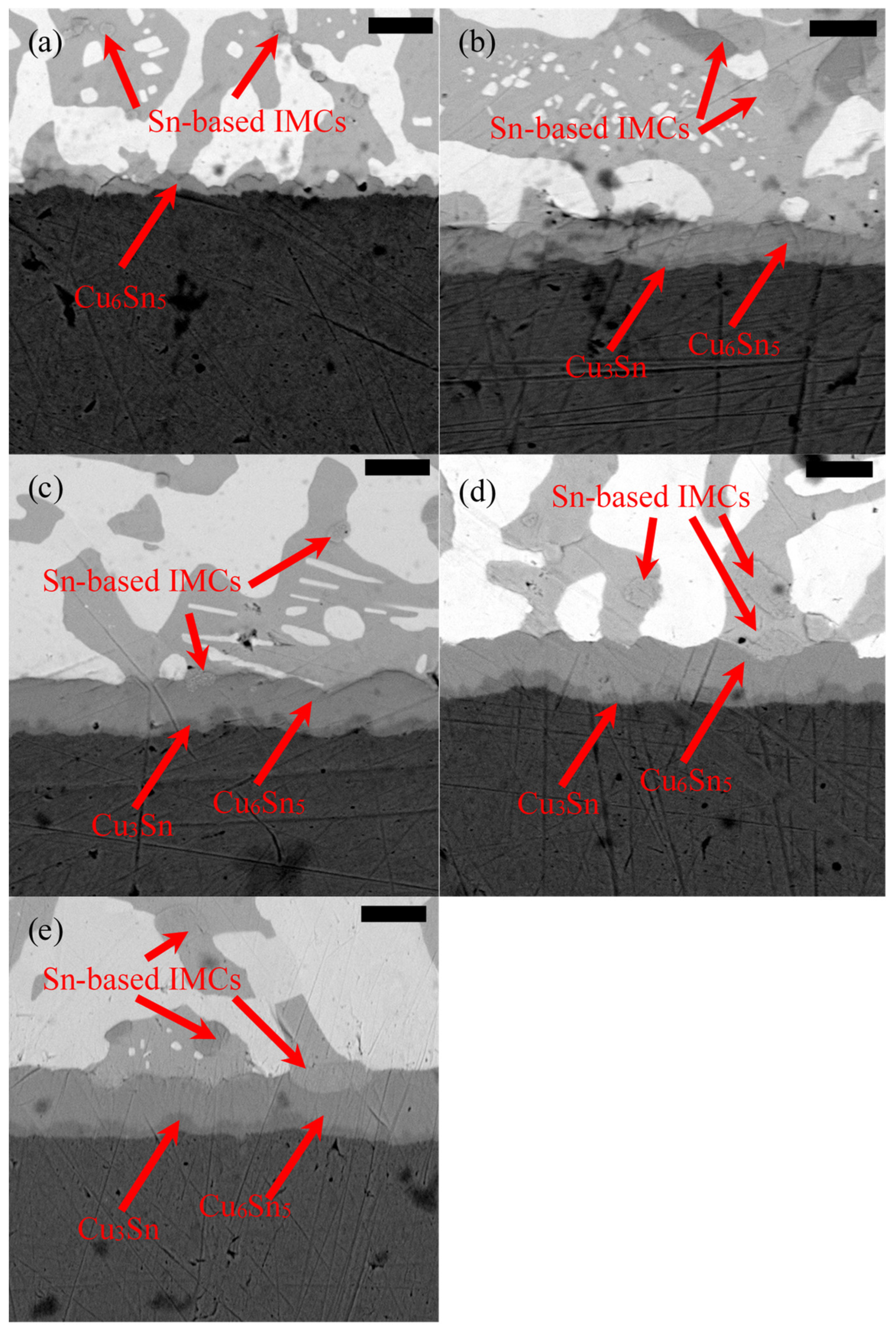
Following initial analysis of the PCB cross-section the board was then subjected to thermal cycling for up to 1000 cycles. A representative SEM analysis is presented in Figure 14, Figure 15, Figure 16 and Figure 17 for each alloy. EDX analysis for samples after 1000 cycles of thermal cycling can be found in the supplementary information (Supplementary Materials, Figures S4-1–S4-5, S5-1–S5-5, S6-1–S6-5 and S7-1–S7-5).
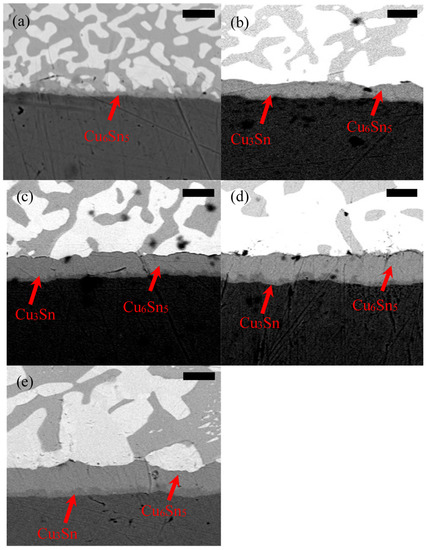
Figure 14.
SEM micrograph of 42Sn58Bi after (a) 0 cycles, (b) 250 cycles, (c) 500 cycles, (d) 750 cycles and (e) 1000 cycles. The scale bar is 4 µm in all images.

Figure 15.
SEM micrograph of 42Sn57Bi1Ag after (a) 0 cycles, (b) 250 cycles, (c) 500 cycles, (d) 750 cycles and (e) 1000 cycles. The scale bar is 4 µm in all images.

Figure 16.
SEM micrograph of LT 47 after (a) 0 cycles, (b) 250 cycles, (c) 500 cycles, (d) 750 cycles and (e) 1000 cycles. The scale bar is 4 µm in all images.

Figure 17.
SEM micrograph of LT 51 after (a) 0 cycles, (b) 250 cycles, (c) 500 cycles, (d) 750 cycles and (e) 1000 cycles. The scale bar is 4 µm in all images.
All 4 alloys seem to behave similarly during the thermal cycling experiments (Figure 14, Figure 15, Figure 16 and Figure 17). Over time the bismuth phase seems to coarsen as does the IMC layer. The bismuth coarsening seems to be less pronounced in LT 47 and LT 51 (Figure 16 and Figure 17). Closer examination of the SEM of these alloys during thermal cycling reveals the presence of tin-based intermetallic compounds in the tin matrix which seem to block coarsening of the bismuth-rich phases. Indeed, this is confirmed by analyzing the %area occupied by the bismuth phases (Table 4). Initially all 4 alloys, with the exception of 42Sn57Bi1Ag account, have similar Bi coverage. After 1000 cycles of thermal cycling the bismuth phases account for a larger %area for 42Sn58Bi and 42Sn57Bi1Ag than both LT47 and LT 51. Solder pastes made with LT 47 and LT 51 were obtained directly from the manufacturer and their metal composition was not disclosed. This should translate to a more mechanically reliable solder joint [28].
Table 4.
% Area covered by Bi phases during each stage of thermal cycling.
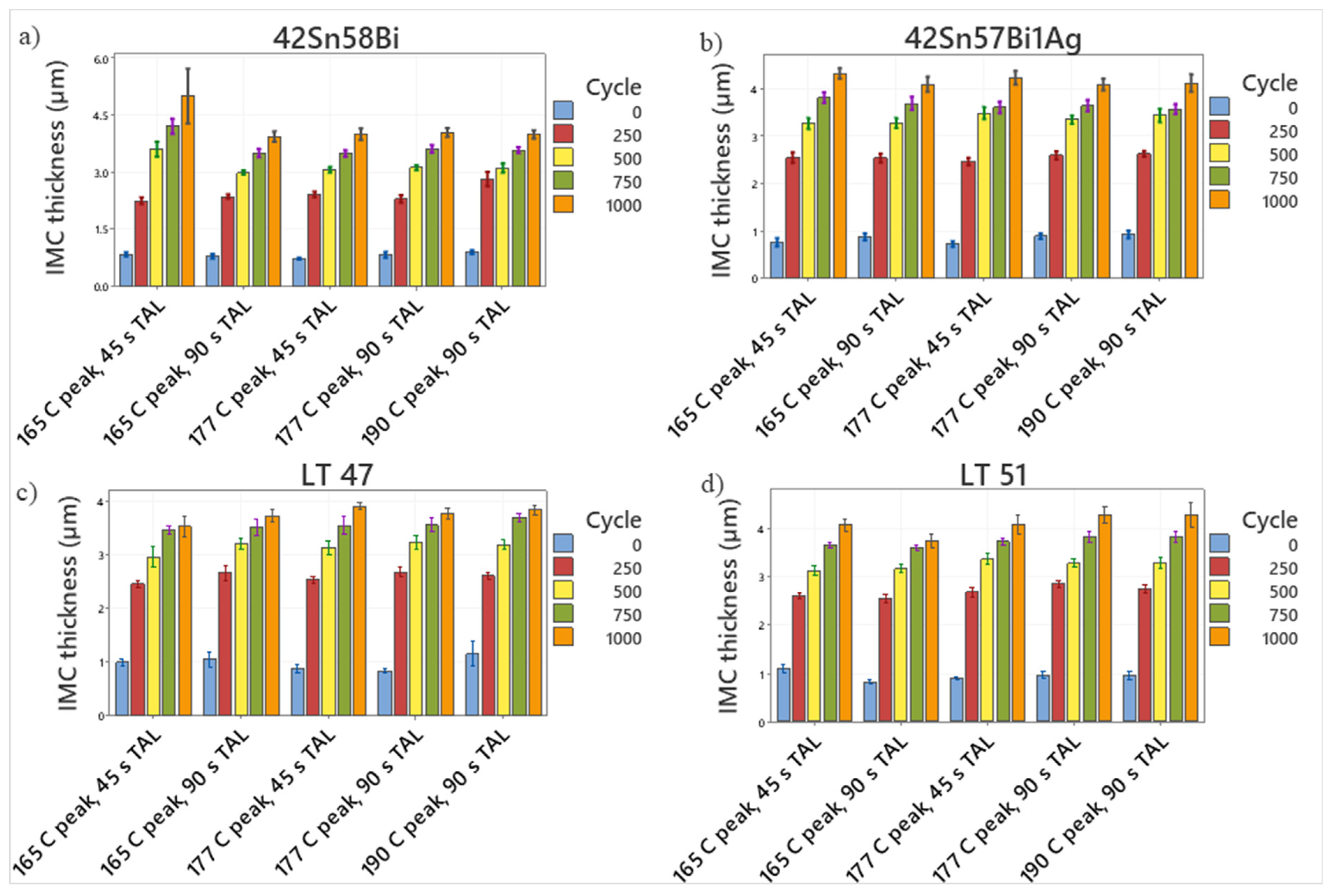
Examination of Figure 14, Figure 15, Figure 16 and Figure 17 reveals a clear trend that the IMC layer coarsens over time. Furthermore, upon closer examination it appears that a new IMC develops in the Sn–Cu matrix. This becomes evident after 250 cycles. This is the point where the IMC layer is composed of Cu3Sn and Cu6Sn5. The coarsening of the IMC layer is thought to be caused by the heating cycles during the thermal cycling experiments. High temperatures are known to favor IMC formation, which is a diffusion-controlled process [38]. Copper-rich Cu3Sn forms near the copper substrate over time while tin-rich Cu6Sn5 forms near the tin matrix. The Cu3Sn IMC layer thickness seems to plateau after 750 cycles. The evolution of the thickness of both the Cu3Sn and the Cu6Sn5 layer was plotted in Figure 18.
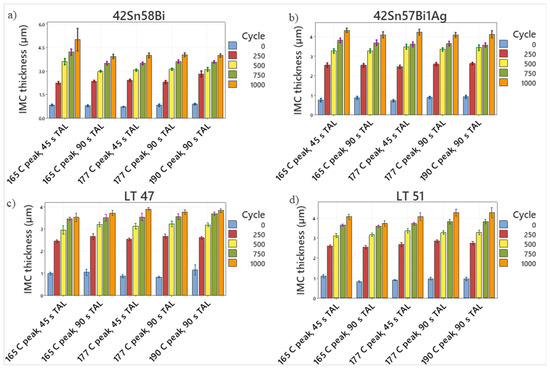
Figure 18.
Charts plotting the evolution of the IMC layer as a function of cycles for (a) 42Sn58Bi, (b) 42Sn57Bi1Ag, (c) LT 47 and (d) LT 51.
Examination of Figure 18 reveals that all four alloys display similar behavior for IMC evolution regardless of the reflow profile used to solder them. It is clear that all four alloys show rapid growth of the IMC layer early on in the process which then seems to plateau as the thermal cycling experiments continue. In order to understand the evolution of the IMC layer during the heating phase of thermal cycling the data was fitted using Equation (1):
IMCt is the IMC thickness at time t in µm, IMC0 is the initial IMC thickness in µm, k is the growth constant (µm min−0.5) and t is time (min) [38].
Assuming that the majority of the IMC growth proceeds during the heating phase of thermal cycling and that each heating cycle is 15 min long, the growth constant for each alloy can be calculated (Figure 19) using Equation (1). The k value at 125 °C for each alloy (Table 5) was calculated by taking the slope from each graph. As the initial reflow profile does not appear to affect intermetallic growth during thermal cycling, the value of k for each alloy was an average of the 5 different values collected for each specific reflow condition.
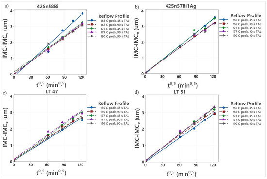
Figure 19.
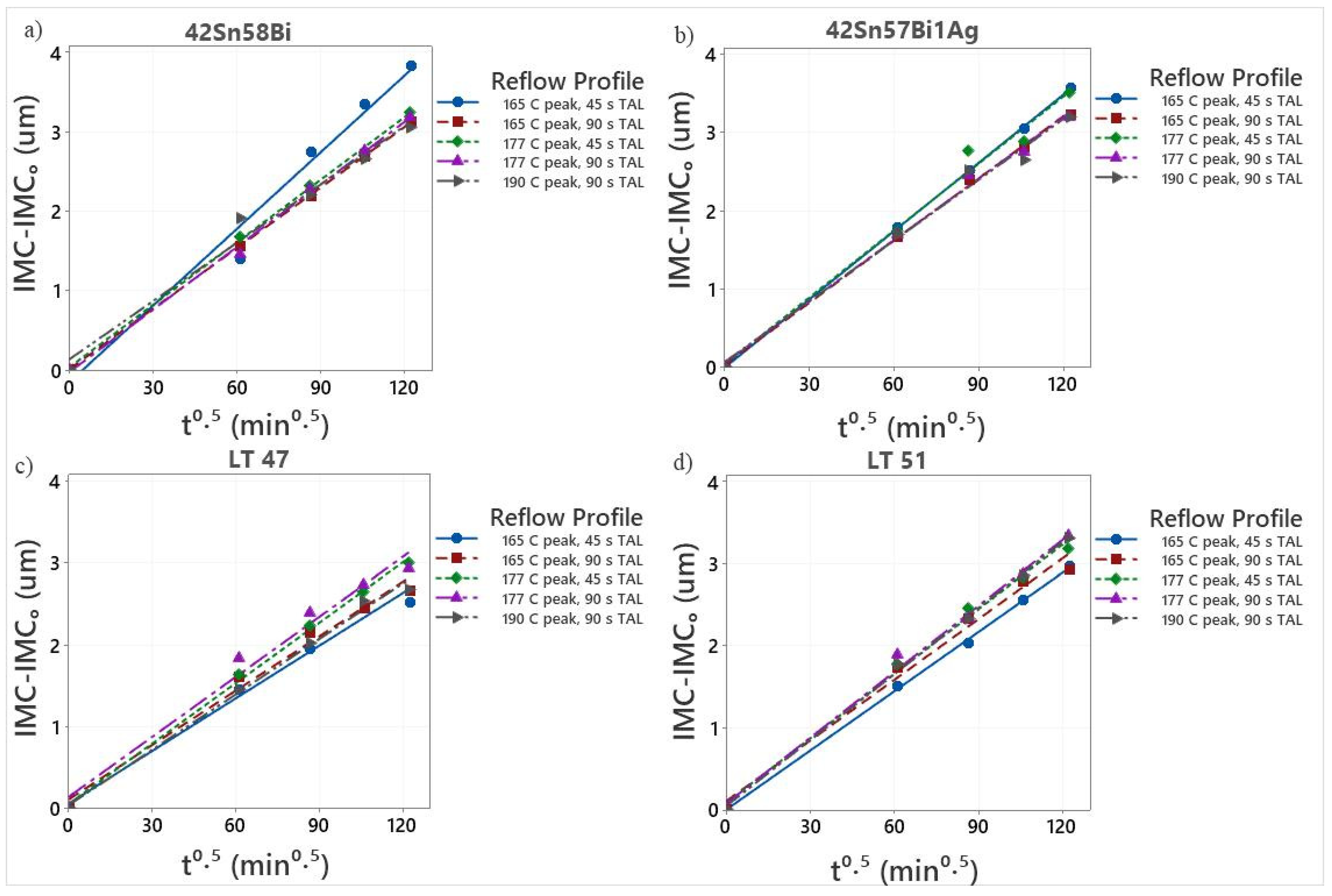
Graph plotting IMC evolution versus square root of time for (a) 42Sn58Bi, (b) 42Sn57Bi1Ag, (c) LT 47 and (d) LT 51.
Table 5.
Value of growth constant, k at 125 °C for tin–bismuth alloys.
All four alloys (Figure 19) show linear growth of the IMC layer when the thickness is plotted against the square root of time. Furthermore, they all display very similar growth constants at 125 °C suggesting that at this temperature, the IMC layer grows at a similar rate regardless of alloy type which is in excellent agreement with the experimental SEM data. This indicates that all four alloys can withstand a broad range of reflow conditions making them ideal candidates for SMT assembly.
4. Conclusions
The current study has demonstrated how four different low temperature alloys behave when subjected to a broad range of reflow conditions in RTS profiles. Printing and reflow experiments indicate that the alloys perform better when using long TALs and high peak temperatures. These types of conditions are favorable for key variables such as wetting performance and voiding levels. It is thought that the interaction between the flux medium, solder alloy and soldered surfaces is more efficient at high peak temperatures and long TALs.
Analysis of the metallurgical properties of the reflowed solder alloys also confirm that they can withstand a broad window of reflow conditions. Reflow profile did not have a dramatic impact on the IMC thickness or microstructure of the reflowed solder joint. Furthermore, the evolution of the IMC layer and microstructure during thermal cycling was very similar for all four alloys 52Sn58Bi, 42Sn57Bi1Ag, LT 47 and LT 51 and all reflow profiles studied. The versatility of Sn–Bi alloys is advantageous for their use in SMT assembly where a vast range of processing conditions are employed depending on the application.
Supplementary Materials
The following are available online at https://www.mdpi.com/article/10.3390/met12010121/s1, Figure S1., SEM/EDx (mapping) analysis of black residue, Figure S2 Representative 2D X-ray images for a QFN32 component reflowed with (a) 42Sn58Bi, (b) 42Sn57Bi1Ag, (c) LT 47 and (d) LT 51. Figure S3: Intermetallic layer with the copper substrate of sample (42Sn58Bi solder alloy, reflow profile (1) before aging analyzed by SEM/EDX (line scan). Figure S4-1: Intermetallic layer with the copper substrate of sample (42Sn58Bi solder alloy, reflow profile 1) after aging (1000 cycles) analyzed by SEM/EDX (line scan). Figure S4-2: Intermetallic layer with the copper substrate of sample (42Sn58Bi solder alloy, reflow profile 2) after aging (1000 cycles) analyzed by SEM/EDX (line scan). Figure S4-3: Intermetallic layer with the copper substrate of sample (42Sn58Bi solder alloy, reflow profile 3) after aging (1000 cycles) analyzed by SEM/EDX (line scan). Figure S4-4: Intermetallic layer with the copper substrate of sample (42Sn58Bi solder alloy, reflow profile 4) after aging (1000 cycles) analyzed by SEM/EDX (line scan). Figure S4-5: Intermetallic layer with the copper substrate of sample (42Sn58Bi solder alloy, reflow profile 5) after aging (1000 cycles) analyzed by SEM/EDX (line scan). Figure S5-1: Intermetallic layer with the copper substrate of sample (42Sn57Bi1Ag solder alloy, reflow profile 1) after aging (1000 cycles) analyzed by SEM/EDX (line scan). Figure S5-2: Intermetallic layer with the copper substrate of sample (42Sn57Bi1Ag solder alloy, reflow profile 2) after aging (1000 cycles) analyzed by SEM/EDX (line scan). Figure S5-3: Intermetallic layer with the copper substrate of sample (42Sn57Bi1Ag solder alloy, reflow profile 3) after aging (1000 cycles) analyzed by SEM/EDX (line scan). Figure S5-4: Intermetallic layer with the copper substrate of sample (42Sn57Bi1Ag solder alloy, reflow profile 4) after aging (1000 cycles) analyzed by SEM/EDX (line scan). Figure S5-5: Intermetallic layer with the copper substrate of sample (42Sn57Bi1Ag solder alloy, reflow profile 5) after aging (1000 cycles) analyzed by SEM/EDX (line scan). Figure S6-1: Intermetallic layer with the copper substrate of sample (LT 47 solder alloy, reflow profile 1) after aging (1000 cycles) analyzed by SEM/EDX (line scan). Figure S6-2: Intermetallic layer with the copper substrate of sample (LT 47 solder alloy, reflow profile 2) after aging (1000 cycles) analyzed by SEM/EDX (line scan). Figure S6-3: Intermetallic layer with the copper substrate of sample (LT 47 solder alloy, reflow profile 3) after aging (1000 cycles) analyzed by SEM/EDX (line scan). Figure S6-4: Intermetallic layer with the copper substrate of sample (LT 47 solder alloy, reflow profile 4) after aging (1000 cycles) analyzed by SEM/EDX (line scan). Figure S6-5: Intermetallic layer with the copper substrate of sample (LT 47 solder alloy, reflow profile 5) after aging (1000 cycles) analyzed by SEM/EDX (line scan). Figure S7-1: Intermetallic layer with the copper substrate of sample (LT 51 solder alloy, reflow profile 1) after aging (1000 cycles) analyzed by SEM/EDX (line scan). Figure S7-2: Intermetallic layer with the copper substrate of sample (LT 51 solder alloy, reflow profile 2) after aging (1000 cycles) analyzed by SEM/EDX (line scan). Figure S7-3: Intermetallic layer with the copper substrate of sample (LT 51 solder alloy, reflow profile 3) after aging (1000 cycles) analyzed by SEM/EDX (line scan). Figure S7-4: Intermetallic layer with the copper substrate of sample (LT 51 solder alloy, reflow profile 4) after aging (1000 cycles) analyzed by SEM/EDX (line scan). Figure S7-5: Intermetallic layer with the copper substrate of sample (LT 51 solder alloy, reflow profile 5) after aging (1000 cycles) analyzed by SEM/EDX (line scan).
Author Contributions
K.D., formal analysis, funding acquisition, investigation, writing—review and editing; D.B., investigation, formal analysis, visualization, writing—review and editing; P.V., investigation, formal analysis, visualization, writing—review and editing; A.P., investigation, formal analysis; M.P., investigation, formal analysis; J.D.R., conceptualization, methodology, investigation, resources, writing—original draft, writing—review and editing. All authors have read and agreed to the published version of the manuscript.
Funding
The work was supported by the Grant Agency of the Czech Technical University in Prague, grant No. SGS21/159/OHK3/3T/13.
Institutional Review Board Statement
Not applicable.
Informed Consent Statement
Not applicable.
Data Availability Statement
The data is available upon request from the corresponding author.
Acknowledgments
The authors wish to acknowledge Itzayana Lopez and Andres Lozoya of Soldadura de Mexico and Yuan Xu of AIM Solder for help with printing experiments.
Conflicts of Interest
The authors declare no conflict of interest.
References
- Lau, C.S.; Khor, C.; Soares, D.; Teixeira, J.; Abdullah, M. Thermo-mechanical challenges of reflowed lead-free solder joints in surface mount components: A review. Solder. Surf. Mt. Technol. 2016, 28, 41–62. [Google Scholar] [CrossRef]
- Pan, J.; Bath, J.; Willie, D.; Toleno, B.J.; Chou, T.-C. Effects of reflow profile and thermal conditioning on intermetallic compound thickness for SnAgCu soldered joints. Solder. Surf. Mt. Technol. 2009, 21, 32–37. [Google Scholar] [CrossRef] [Green Version]
- Salam, B.; Virseda, C.; Da, H.; Ekere, N.; Durairaj, R. Reflow profile study of the Sn-Ag-Cu solder. Solder. Surf. Mt. Technol. 2004, 16, 27–34. [Google Scholar] [CrossRef]
- Tan, W.; Ume, I.C.; Hung, Y.; Wu, C.F.J. Effects of Warpage on Fatigue Reliability of Solder Bumps: Experimental and Analytical Studies. IEEE Trans. Adv. Packag. 2010, 33, 314–322. [Google Scholar] [CrossRef]
- Ogunseitan, O.A. Public health and environmental benefits of adopting lead-free solders. JOM 2007, 59, 12–17. [Google Scholar] [CrossRef]
- Jiang, N.; Zhang, L.; Liu, Z.-Q.; Sun, L.; Long, W.-M.; He, P.; Xiong, M.-Y.; Zhao, M. Reliability issues of lead-free solder joints in electronic devices. Sci. Technol. Adv. Mater. 2019, 20, 876–901. [Google Scholar] [CrossRef] [PubMed] [Green Version]
- Siewart, T.; Liu, S.; Smith, D.R.; Madeni, J.C. Database for Solder Properties with Emphasis on New Lead-free Solders. In Properties of Lead-Free Solders; National Institute of Standards: Gaithersburg, MD, USA, 2002. [Google Scholar] [CrossRef]
- Schwaneke, A.E.; Falke, W.L.; Miller, V.R. Surface tension and density of liquid tin-lead solder alloys. J. Chem. Eng. Data 1978, 23, 298–301. [Google Scholar] [CrossRef]
- Gan, K.; Ngan, A. The unusual size effect of eutectic Sn/Pb alloys in the micro regime: Experiments and modeling. Acta Mater. 2018, 151, 282–292. [Google Scholar] [CrossRef]
- Kang, S.K.; Lauro, P.; Shih, D.-Y.; Henderson, D.W.; Puttlitz, K.J. Microstructure and mechanical properties of lead-free solders and solder joints used in microelectronic applications. IBM J. Res. Dev. 2005, 49, 607–620. [Google Scholar] [CrossRef]
- Hammad, A. Enhancing the ductility and mechanical behavior of Sn-1.0Ag-0.5Cu lead-free solder by adding trace amount of elements Ni and Sb. Microelectron. Reliab. 2018, 87, 133–141. [Google Scholar] [CrossRef]
- Olofinjana, A.; Haque, R.; Mathir, M.; Voo, N. Studies of the solidification characteristics in Sn-Ag-Cu-Bi solder alloys. Procedia Manuf. 2019, 30, 596–603. [Google Scholar] [CrossRef]
- Rahman, A.R.A.; Nayan, N.A. Critical challenges and solutions for device miniaturization in integrated circuit packaging technology. J. Eng. Appl. Sci. 2018, 13, 6025–6032. [Google Scholar] [CrossRef]
- Shao, S.; Liu, D.; Niu, Y.; O’Donnell, K.; Sengupta, D.; Park, S. A Study on the Thermomechanical Reliability Risks of Through-Silicon-Vias in Sensor Applications. Sensors 2017, 17, 322. [Google Scholar] [CrossRef] [Green Version]
- Esfandyari, A.; Syed-Khaja, A.; Javied, T.; Franke, J. Energy Efficiency Investigation on High-Pressure Convection Reflow Soldering in Electronics Production. Appl. Mech. Mater. 2014, 655, 95–100. [Google Scholar] [CrossRef]
- Shen, Y.-A.; Zhou, S.; Li, J.; Yang, C.-H.; Huang, S.; Lin, S.-K.; Nishikawa, H. Sn-3.0Ag-0.5Cu/Sn-58Bi composite solder joint assembled using a low-temperature reflow process for PoP technology. Mater. Des. 2019, 183, 108144. [Google Scholar] [CrossRef]
- Frear, D.R. Issues related to the implementation of Pb-free electronic solders in consumer electronics. J. Mater. Sci. Mater. Electron. 2006, 18, 319–330. [Google Scholar] [CrossRef]
- Kotadia, H.R.; Howes, P.; Mannan, S. A review: On the development of low melting temperature Pb-free solders. Microelectron. Reliab. 2014, 54, 1253–1273. [Google Scholar] [CrossRef]
- George, E.; Pecht, M. RoHS compliance in safety and reliability critical electronics. Microelectron. Reliab. 2016, 65, 1–7. [Google Scholar] [CrossRef]
- Miao, H.-W.; Duh, J.-G.; Chiou, B.-S. Thermal cycling test in Sn-Bi and Sn-Bi-Cu solder joints. J. Mater. Sci. Mater. Electron. 2000, 11, 609–618. [Google Scholar] [CrossRef]
- Wang, F.; Chen, H.; Huang, Y.; Liu, L.; Zhang, Z. Recent progress on the development of Sn–Bi based low-temperature Pb-free solders. J. Mater. Sci. Mater. Electron. 2019, 30, 3222–3243. [Google Scholar] [CrossRef]
- Gusakova, O.V.; Galenko, P.K.; Shepelevich, V.; Alexandrov, D.V.; Rettenmayr, M. Diffusionless (chemically partitionless) crystallization and subsequent decomposition of supersaturated solid solutions in Sn–Bi eutectic alloy. Philos. Trans. R. Soc. A Math. Phys. Eng. Sci. 2019, 377, 20180204. [Google Scholar] [CrossRef] [Green Version]
- Wang, J.; Wei, H.; He, P.; Lin, T.; Lu, F. Microstructure and Mechanical Properties of Tin-Bismuth Solder Reinforced by Aluminum Borate Whiskers. J. Electron. Mater. 2015, 44, 3872–3879. [Google Scholar] [CrossRef]
- Shimokawa, H.; Soga, T.; Serizawa, K.; Katayama, K.; Shohji, I. Evaluation on Mechanical Properties of Sn-Bi-Ag Solder and Reliability of the Solder Joint. Trans. Jpn. Inst. Electron. Packag. 2015, 8, 46–54. [Google Scholar] [CrossRef] [Green Version]
- Huang, Y.-C.; Chen, S.-W. Effects of Co Alloying and Size on Solidification and Interfacial Reactions in Sn-57 wt.%Bi-(Co)/Cu Couples. J. Electron. Mater. 2011, 40, 62–70. [Google Scholar] [CrossRef]
- Gain, A.K.; Zhang, L. Growth mechanism of intermetallic compound and mechanical properties of nickel (Ni) nanoparticle doped low melting temperature tin–bismuth (Sn–Bi) solder. J. Mater. Sci. Mater. Electron. 2016, 27, 781–794. [Google Scholar] [CrossRef]
- McCormack, M.; Chen, H.S.; Kammlott, G.W.; Jin, S. Significantly Improved Mechanical Properties of Bi-Sn Solder Alloys by Ag- Doping. J. Electron. Mater. 1997, 26, 954–958. [Google Scholar] [CrossRef]
- Ren, G.; Collins, M.N. Improved Reliability and Mechanical Performance of Ag Microalloyed Sn58Bi Solder Alloys. Metals 2019, 9, 462. [Google Scholar] [CrossRef] [Green Version]
- Melton, C. Effect of Solder Reflow Process Variables on the Solder Wettability of Lead Free Solder Alloys. Solder. Surf. Mt. Technol. 1994, 6, 20–29. [Google Scholar] [CrossRef]
- Pan, J.; Chou, T.C.; Dee, W.J.; Toleno, B.J. Effect of reflow profile on SnPb and SnAgCu solder joint shear force. IPC—Print. Circuits Expo, Apex, Des. Summit 2006 Perfectly Cut. Edge 2006, 2, 1010–1019. [Google Scholar]
- Shen, J.; Pu, Y.; Yin, H.; Luo, D.; Chen, J. Effects of minor Cu and Zn additions on the thermal, microstructure and tensile properties of Sn–Bi-based solder alloys. J. Alloy. Compd. 2014, 614, 63–70. [Google Scholar] [CrossRef]
- Choi, J.Y.; Park, D.; Oh, T.S. Chip Interconnection Process for Smart Fabrics Using Flip-chip Bonding of SnBi Solder. J. Microelectron. Packag. Soc. 2012, 19, 71–76. [Google Scholar] [CrossRef] [Green Version]
- Li, M.-L.; Zhang, L.; Jiang, N.; Zhang, L.; Zhong, S.-J. Materials modification of the lead-free solders incorporated with micro/nano-sized particles: A review. Mater. Des. 2021, 197, 109224. [Google Scholar] [CrossRef]
- Yunus, M.; Primavera, A.; Srihari, K.; Pitarresi, J. Effect of voids on the reliability of BGA/CSP solder joints. In Proceedings of the Twenty Sixth IEEE/CPMT International Electronics Manufacturing Technology Symposium, Santa Clara, CA, USA, 6 August 2002. [Google Scholar]
- Lee, S.W.R.; Song, F. Impact of IMC Thickness on Lead-free Solder Joint Reliability under Thermal Aging: Ball Shear Tests vs. Cold Bump Pull Tests. In Proceedings of the 2006 International Microsystems, Package, Assembly Conference Taiwan, Taipei, Taiwan, 18–20 October 2006; IEEE: Piscataway, NJ, USA; pp. 1–4. [Google Scholar]
- Li, W.-X.; Stampfl, C.; Scheffler, M. Why is a Noble Metal Catalytically Active? The Role of the O-Ag Interaction in the Function of Silver as an Oxidation Catalyst. Phys. Rev. Lett. 2003, 90, 256102. [Google Scholar] [CrossRef] [Green Version]
- Herron, D.; Liu, Y.; Lee, N.-C. Effective voiding control of QFN via solder mask patterning. In Proceedings of the 2013 IEEE 63rd Electronic Components and Technology Conference, Las Vegas, NV, USA, 28–31 May 2013; IEEE: Piscataway, NJ, USA; pp. 468–474. [Google Scholar]
- Wierzbicka-Miernik, A.; Miernik, K.; Filipek, R.; Szyszkiewicz, K. Kinetics of intermetallic phase growth and determination of diffusion coefficients in solid–solid-state reaction between Cu and (Sn+1at.%Ni) pads. J. Mater. Sci. 2017, 52, 10533–10544. [Google Scholar] [CrossRef] [Green Version]

Publisher’s Note: MDPI stays neutral with regard to jurisdictional claims in published maps and institutional affiliations. |
© 2022 by the authors. Licensee MDPI, Basel, Switzerland. This article is an open access article distributed under the terms and conditions of the Creative Commons Attribution (CC BY) license (https://creativecommons.org/licenses/by/4.0/).