Article

Ti Interlayer Mediated Uniform NiGe Formation under Low-Temperature Microwave Annealing

1
School of Mathematics, Physics and Statistics, Shanghai University of Engineering Science, Shanghai 201600, China
2
State Key Laboratory of Functional Material for Informatics, Shanghai Institute of Microsystem and Information Technology, CAS, Shanghai 200050, China
*
Authors to whom correspondence should be addressed.
Metals 2021, 11(3), 488; https://doi.org/10.3390/met11030488
Submission received: 24 December 2020 / Revised: 1 March 2021 / Accepted: 11 March 2021 / Published: 15 March 2021

Abstract

:
The reactions between nickel and germanium are investigated by the incorporation of a titanium interlayer on germanium (100) substrate. Under microwave annealing (MWA), the nickel germanide layers are formed from 150 °C to 350 °C for 360 s in ambient nitrogen atmosphere. It is found that the best quality nickel germanide is achieved by microwave annealing at 350 °C. The titanium interlayer becomes a titanium cap layer after annealing. Increasing the diffusion of Ni by MWA and decreasing the diffusion of Ni by Ti are ascribed to induce the uniform formation of nickel germanide layer at low MWA temperature.

1. Introduction

Germanium (Ge) has attracted a great deal of contemporary interest as a channel material in high-performance transistors, due to its higher hole and electron mobility than Si [1,2,3]. Due to nickel germanide (NixGey) having the advantages of low resistivity, low formation temperature, and the feasibility of self-aligned germination process [4,5], it has been selected as the most promising contact material for Ge-based Metal-Oxide-Semiconductor Field-Effect Transistor (MOSFET) devices. However, one major drawback of NixGey is its rough interface due to polycrystalline grains and agglomeration at high annealing temperatures (500–550 °C). It was reported that the thermal stability of NixGey on bulk Ge could be improved by pre-germanidation implantation [6], prior-germanidation fluorine implantation into Ge substrate [7], dopant segregation [8], or introducing other elements, such as titanium (Ti) [9], platinum (Pt) [10], tungsten (W) [11], tantalum (Ta) [11,12], cobalt (Co) [13], ytterbium (Yb) [14], and so on.
On the other hand, various annealing methods have been used to prepare NixGey films, such as rapid thermal annealing (RTA) [15] and laser annealing [16]. However, these methods have some limitations. Halogen lamp rapid thermal processing technology has problems such as high thermal budget, uneven heating, and a large residual defect density. For the laser annealing method, the spot size is small which will take a great deal of time to cover the entire surface area of a sample. Microwave heating has increasingly attracted attention in several industrial applications. For example, previous research has shown that low-temperature microwave annealing may be an alternative to other rapid thermal processing methods in silicon processing [17,18,19]. Oghbaei et al. reported that microwave annealing (MWA) reduces energy consumption, processing time, and annealing temperature [20]. Hu et al. reported that the formation of low-resistivity nickel germanosilide (NiSiGe) film via microwave heating occurs at temperatures about 100 °C lower than using RTA [21]. For the Ni/Ge systems, there are few studies which focus on the Ni–Ge solid-state reaction under MWA. Hsu et al. studied the effects of a Pt interlayer on the structural and electrical properties of NixGey through MWA and found the Pt interlayers played a role during the alloy formation by preventing rapid Ni diffusion [22]. However, the formation of a NixGey layer in the appearance of other metals under MWA has not been fully investigated.
In this study, we investigated the formation of NixGey layers by Ti incorporation on a Ge (100) substrate under MWA. It was found that the formation of uniform nickel germanide layer could be achieved under MWA at 350 °C. Most of the Ti atoms moved to the surface of the NiGe layer after annealing. The mechanism analysis of MWA and the effects of Ti mediation are discussed in detail.

2. Experimental

Pure Ge(001) substrates were used in this study. The Radio Corporation of America (RCA) standard clean 1 (SC1), consisting of NH4OH:H2O2:H2O at a 1/2/20 ratio and temperature of 60 °C for 10 min was used to remove the organics, certain metals, and particles. The RCA standard clean 2 (SC2), consisting of HCl:H2O2:H2O at 1/1/20 ratio and temperature of 60 °C for 10 min is used to remove metallic contamination. In order to remove germanium oxides on the surface, the Ge substrates were cleaned using a dilute fluoric acid (1% HF) for 60 s. Then, a 1 nm Ti intermediate layer and a 10 nm Ni layer were successively deposited on the Ge (100) substrate by using electron beam evaporation. After the deposition, these wafers were sliced into pieces of 2.0 cm × 2.0 cm. Then, the samples were annealed in an AXOM-200 (Manufactured by DSG Technologies) MWA chamber (5.8 GHz) at 150 °C, 200 °C, 250 °C, 300 °C, and 350 °C for 360 s in an ambient nitrogen atmosphere. The temperature image after calibration and the error of each temperature are shown in Appendix A (Figure A1 and Table A1). The MWA chamber is designed for multi-wafer processing; the vertically stacked wafers are supported by three quartz rods inside a quartz chamber. The card slot on the quartz column can satisfy the annealing of several wafers together. The three adjustable quartz columns make the equipment suitable for 4, 6, and 8 inch wafer annealing. All samples were located inside the middle of the chamber where the electromagnetic field was uniform. An infrared pyrometer located at the bottom of the chamber was used to directly monitor the sample temperature. Different temperatures could be achieved by adjusting the input power to generate continuous microwave output from 10% to 100% of the maximum rated microwave power output. To avoid oxidation, the nitrogen flow was maintained until the annealing process was completed.
The as-prepared NixGey samples were characterized by four-point probe (FPP) measurements for sheet resistance (Rsh), Raman spectroscopy (Raman) for phase formation identification, transmission electron microscopy (TEM) for morphology and microstructure observations, and energy dispersive spectrometer (EDS) for elemental mapping and line scans in NixGey films.

3. Results and Discussion

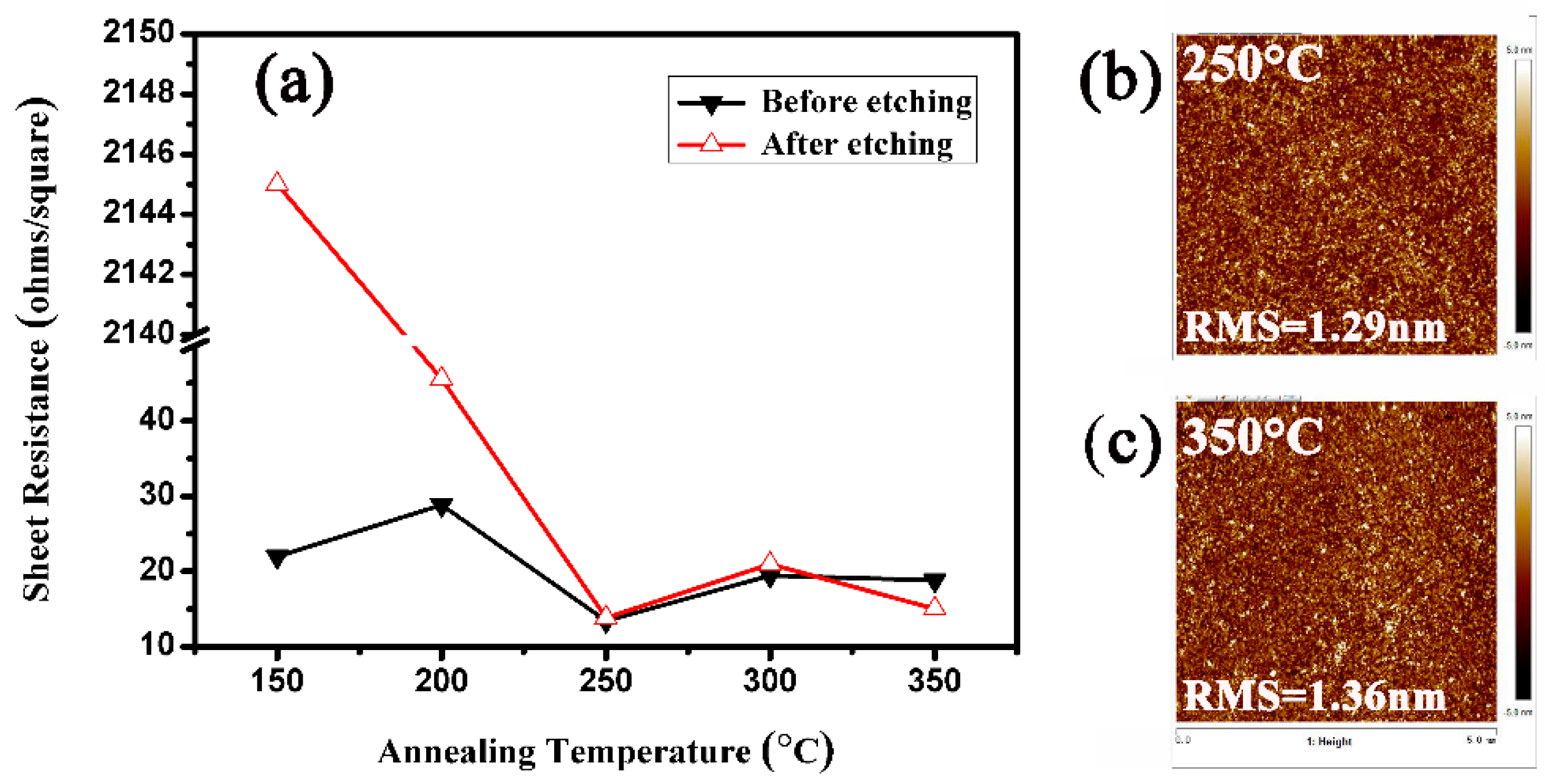
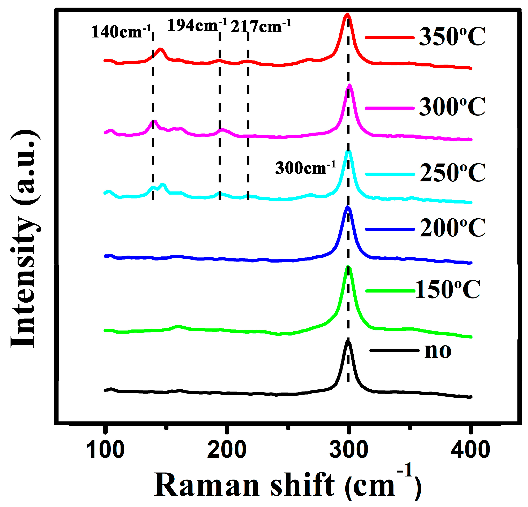
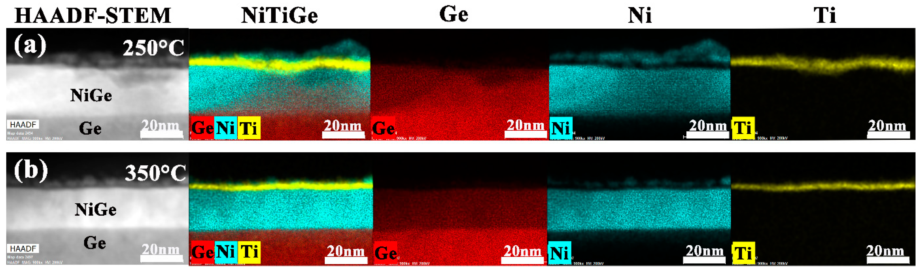
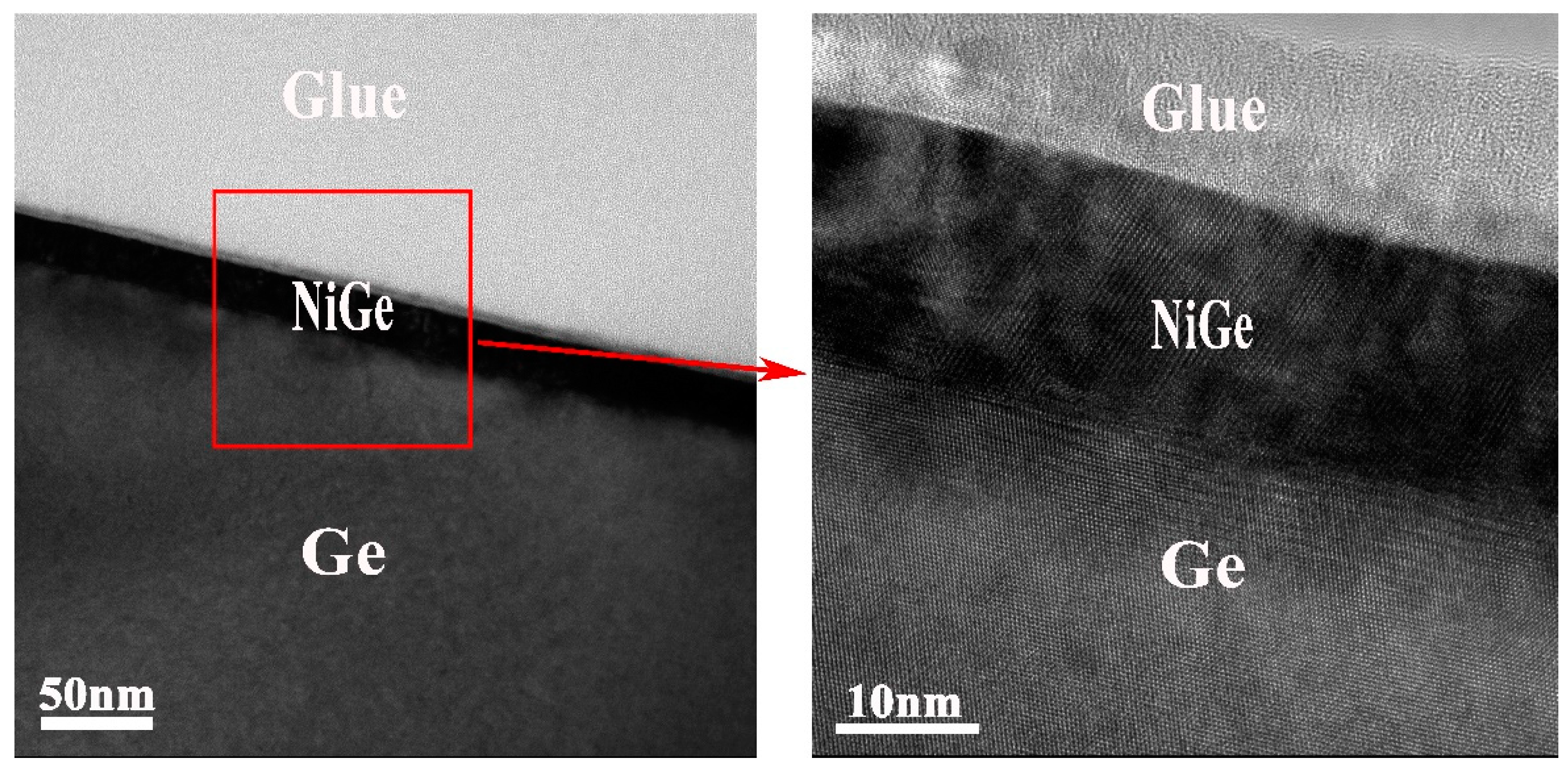
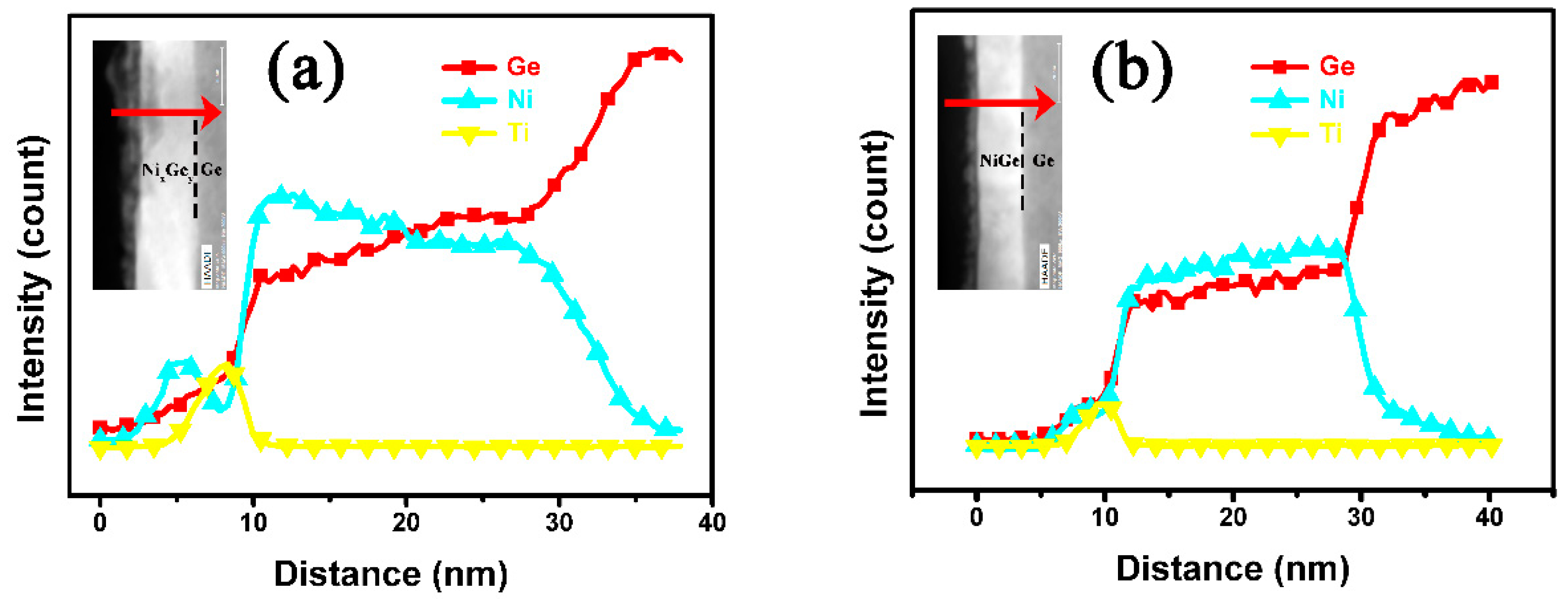
3.1. Characterization of the NixGey Layers

The influence of MWA on the nickel germanide formed on a Ge substrate was studied by measuring sheet resistance. The variation of sheet resistance (Rsh) with germanidation temperature is shown in Figure 1a. At 150 °C, the sheet resistance value is very large after etching, which indicates that Ni has not reacted with Ge. This result could be also confirmed by the Raman analysis, as shown in Figure 2. The sheet resistance value decreased gradually after annealed at 200 °C, indicating the Ni-rich phase (Ni2Ge or Ni5Ge3) with higher resistance transition to the Ni mono-nickel germanide phase (NiGe) [23,24,25]. In addition, in order to calculate the morphology and roughness of the NixGey layers, AFM roughness analysis was carried out, as shown in Figure 1b,c. According to the AFM measurements, it was found that the films were smooth, and the root mean square surface roughness increased slightly from 1.29 nm to 1.36 nm.
Figure 2 shows the Raman spectra of the as-deposited and annealed samples at temperatures ranging from 150 to 350 °C. For the as-deposited and 150/200 °C annealed samples, no Ni–Ge bond vibrational Raman signal is observed and only the characteristic peak of Ge–Ge bond vibration is shown at 300 cm−1, which indicates that no NixGey phase is formed at these temperatures. After annealing from 250–350 °C, three main Raman peaks are found to be approximately located at 140 cm−1, 194 cm−1 and 217 cm−1, which could be attributed to the NiGe phase [26,27].
In order to further study the structures of germanide layer, the images of high-angle annular dark field scanning TEM (HAADF-STEM) and EDS mappings of the stacking structure are shown in Figure 3, respectively. At 250 °C, there are some grains in the germanide layer, which induced non-uniform Ni element distribution. In addition, it was found that there was some un-reacted Ni on the surface of the germanide layer. It shows that after annealing at 250 °C, Ni had not completely reacted with Ge. After annealing at a relative higher temperature 350 °C, we noticed that there was a clear interface between the Ge substrate and the germanide layer. The NiGe/Ge interface was ideal, and NiGe layer was very smooth without grains. Moreover, as shown in the EDS mapping, for the region which the Ni and Ge mixed, a significant Ni distribution indicates the formation of a nickel germanide layer. It can be seen from the image that the Ti atoms have diffused into the sample surface, which changed from the interlayer to the surface coating of the sample. Compared with the sample annealing at 250 °C, the titanium layer on the surface is smoother, which indicates that the film has good uniformity after annealing at 350 °C.
Figure 4 shows the high-resolution TEM (HRTEM) images of Ni/Ti/Ge samples after MWA at 350 °C. It was found that the NiGe layer was continuous and uniform. The enlarged view shows the NiGe lattice interface image had a good polycrystalline structure and its thickness was about 20 nm. Relative uniformity of the NiGe film and a distinct interface between the NiGe and Ge could be observed. Combining the results of Figure 3b and Figure 5b, we believe that a uniform NiGe layer can be obtained under MWA at 350 °C.
For NixGey films formed with MWA at 250 °C and 350 °C, the EDS measurement depth profiles for different elements are displayed in Figure 5a,b, respectively. We found that Ti atoms were mainly located in the surface area of the NixGey film when Ni reacted with Ge to form germanide, which is consistent with our previous reports [28]. The EDS line profiles suggest that in the region where the Ni and Ge mixed, the 20 nm nickel germanide layer was formed, which is consistent with the HRTEM results, as shown in Figure 4. For the MWA sample at 250 °C, a nickel peak appeared on the surface of the sample and the signal distribution of Ni and Ge in the middle part was uneven, indicated that some Ni-rich phases were formed (see Figure 5a). However, for the 350 °C MWA sample, as shown in Figure 5b, the Ni and Ge intensity was uniformly distributed, which confirmed that the formation of the mono-germanide phase (NiGe).

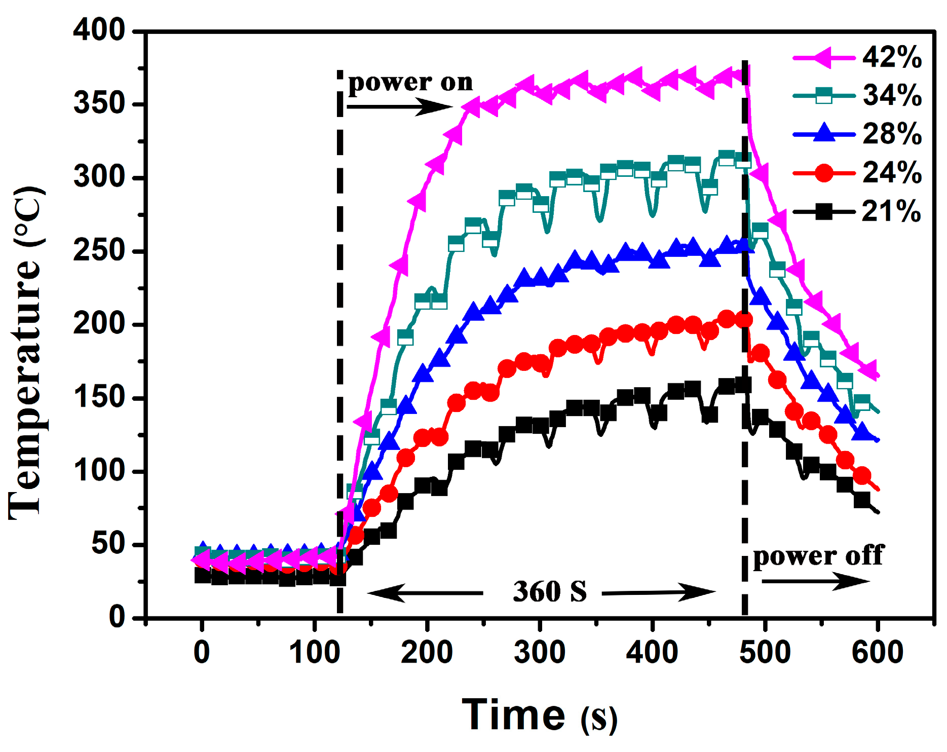
3.2. Mechanism Analysis of MWA

For NiGe formed on Ge, we suspect that dielectric loss and conductivity loss are two possible properties responsible for the microwave losses during microwave annealing [21]. For the dielectric loss, it is caused not only by the lattice vibrational modes, but also by impurities, second phases, pores, lattice defects, grain boundaries, and grain morphology [29]. The point defects generated in Ni–Ge interactions and the grain boundaries of polycrystalline NiGe grains could affect the dielectric loss under MWA. For the conductivity loss, the layers stacked in our samples Ni/Ti/Ge are expected to be heated differently, because the loss factor of different materials determines its absorption of the propagating electric field. According to Ampere’s and Faraday’s laws [30], the effectiveness of electromagnetic field penetration depends on a parameter referred to as the skin depth. With the increase in conductivity, skin depth decreases, and heating can occur in the skin depth layer [31]. Due to the conductivity of Ni (1.46 × 10⁷ s/m) being much greater than that of Ge (2 s/m) [32], the temperature of the Ni layer is higher than the Ge substrate under microwave heating. The high temperature of the Ni layer will also lead to the enhancement of the Ni diffusion rate.

3.3. The Benefits of MWA

Previous research [21] has shown that the local temperature at the substrate front surface where silicidation occurs is higher for the MWA than RTA samples. A local temperature difference at the reaction interface is a reason for the dissimilarity between MWA and RTA. For the RTA process, it is well known that the Ni–Ge reaction starts at 250 °C and a Ti thin film reacts on a Ge substrate above 400 °C [33]. However, under MWA, we found that the mono-germanide phase can be formed at 350 °C in the Ni/Ti/Ge system. The contribution of microwave energy to overcome the activation energy (Ea) is an important factor for NiGe formation, because Ea could be overcome by the combination of substrate temperature and direct coupling of microwave energy into the lattice [34]. Thus, the mono-NiGe phase formed at lower temperatures, similar to the formation of low-resistivity NiSiGe film via MWA which occurs at temperatures about 100 °C lower than using RTA [21].

3.4. The Effect of Ti Mediation under MWA

Zhu et al. reported that the Ti interlayer is expelled to the surface and forms a ternary Ni1−xTixGe phase under RTA 450 °C [9]. Under MWA, the 1 nm Ti interlayer is also totally moved to the surface. However, Ti does not react with Ge in the Ni/Ti/Ge system under MWA at 350 °C, corresponding to the findings that a Ti layer could only react with Ge substrates above 400 °C [33]. The Ti interlayer becomes a perfect cap-layer on the top of NiGe, which could further “protect” the contact property of NiGe. Moreover, it is reported that the Pt interlayer plays a role in preventing the rapid diffusion of Ni and forms PtGe(Ni) and NiGe(Pt) in Ni/Pt/Ge system [22] under the MWA process. The Ti interlayer, like the Pt interlayers, may act as a diffusion barrier to change the Gibbs energy of the NiGe grains and reduce the NiGe growth rate. Similar phenomena have also been found in the cases of Ni/Ti/Si [34], Ni/Ti/SiGe [28] and Ni/Ti/Ge [9] systems.
Based on the above discussion, we propose that two effects, increasing the diffusion of Ni-Ge by MWA and decreasing the diffusion of Ni-Ge by Ti, both occur and reach a balance at some MWA temperatures. However, the detailed mechanisms of Ti on the formation of NiGe under MWA are still not fully understood and require further investigations.

4. Conclusions

In summary, we have investigated the reactions between Ni and Ge in the appearance of a Ti interlayer under MWA processed. The variation of sheet resistance, evolution of surface, and interfacial morphology with different germanidation temperature were investigated systematically. It was demonstrated that by mediation of the Ti interlayer, a flat and uniform NiGe layer was formed at 350 °C. The Ti atoms were found to segregate at the surface of NiGe after annealing. It as shown that MWA is a viable alternative method for the formation of NiGe films at low temperatures. Achieved results in this work could be a potential precursor for S/D contact technology in state-of-the-art Ge-based devices.

Author Contributions

Conceptualization, J.Y., Y.P. and B.Z.; data curation, J.Y.; funding acquisition, Y.P. and B.Z.; investigation, J.Y. and W.L.; supervision and project administration, Y.P., W.Y., Z.X., X.W., A.W. and B.Z.; writing—original draft preparation, J.Y.; writing—review and editing, Y.P. and B.Z.; All authors have read and agreed to the published version of the manuscript.

Funding

This research was funded by the National Natural Science Foundation of China, grant numbers 61604094.

Institutional Review Board Statement

Not applicable.

Informed Consent Statement

Not applicable.

Data Availability Statement

The data presented in this study are available on request from the corresponding author.

Conflicts of Interest

The authors declare no conflict of interest.

Appendix A

In our experiment, MWA equipment used an infrared pyrometer to measure the temperature of the sample. However, in the non-contact infrared temperature measurement, the measured temperature deviated from the actual temperature, so it was necessary to calibrate the temperature. The temperature image after calibration is shown in Figure A1. In addition, due to the limitation of the infrared pyrometer (especially for the low temperature), we provide an error for each temperature, as shown in Table A1.
Figure A1. Annealing temperature curve of the actual sample after calibration.
Metals 11 00488 g0a1
Table A1. Temperature deviation in microwave annealing.
Microwave Annealing
Temperature (°C)
Minimum Temperature (°C)Maximum Temperature (°C)
150130160
200173202
250233257
300277314
350342366

References

  1. Chi On, C.; Hyoungsub, K.; Chi, D.; Triplett, B.B.; McIntyre, P.C.; Saraswat, K.C. A sub-400/spl deg/C germanium MOSFET technology with high-/spl kappa/dielectric and metal gate, Digest. In Proceedings of the International Electron Devices Meeting, San Francisco, CA, USA, 8–11 December 2002; IEEE: New York, NY, USA, 2002; pp. 437–440. [Google Scholar] [CrossRef]
  2. Huiling, S.; Okorn-Schmidt, H.; Chan, K.K.; Copel, M.; Ott, J.A.; Kozlowski, P.M.; Steen, S.E.; Cordes, S.A.; Wong, H.P.; Jones, E.C.; et al. High mobility p-channel germanium MOSFETs with a thin Ge oxynitride gate dielectric, Digest. In Proceedings of the International Electron Devices Meeting, San Francisco, CA, USA, 8–11 December 2002; IEEE: New York, NY, USA, 2002; pp. 441–444. [Google Scholar] [CrossRef]
  3. Zhu, S.; Li, R.; Lee, S.J.; Li, M.F.; Du, A.; Singh, J.; Zhu, C.; Chin, A.; Kwong, D.L. Germanium pMOSFETs with Schottky-barrier germanide S/D, high-/spl kappa/gate dielectric and metal gate. IEEE Electron Device Lett. 2005, 26, 81–83. [Google Scholar] [CrossRef]
  4. Hsu, S.-L.; Chien, C.-H.; Yang, M.-J.; Huang, R.-H.; Leu, C.-C.; Shen, S.-W.; Yang, T.-H. Study of thermal stability of nickel monogermanide on single- and polycrystalline germanium substrates. Appl. Phys. Lett. 2005, 86, 251906. [Google Scholar] [CrossRef] [Green Version]
  5. Zhang, Q.; Wu, N.; Osipowicz, T.; Bera, L.K.; Zhu, C. Formation and Thermal Stability of Nickel Germanide on Germanium Substrate. Jpn. J. Appl. Phys. 2005, 44, L1389–L1391. [Google Scholar] [CrossRef] [Green Version]
  6. Liu, Y.; Xu, J.; Liu, J.; Wang, G.; Luo, X.; Zhang, D.; Mao, S.; Li, Y.; Li, J.; Zhao, C.; et al. Role of Carbon Pre-Germanidation Implantation on Enhancing the Thermal Stability of NiGe Films Below 10 nm Thickness. ECS J. Solid State Sci. Technol. 2020, 9, 054006. [Google Scholar] [CrossRef]
  7. Duan, N.; Wang, G.; Xu, J.; Mao, S.; Luo, X.; Zhang, D.; Wang, W.; Chen, D.; Li, J.; Liu, S.; et al. Enhancing the thermal stability of NiGe by prior-germanidation fluorine implantation into Ge substrate. Jpn. J. Appl. Phys. 2018, 57, 07MA03. [Google Scholar] [CrossRef]
  8. Chen, Z.; Yuan, S.; Li, J.; Zhang, R. Thermal Stability Enhancement of NiGe Metal Source/Drain and Ge pMOSFETs by Dopant Segregation. IEEE Trans. Electron Devices 2019, 66, 5284–5288. [Google Scholar] [CrossRef]
  9. Zhu, S.; Yu, M.B.; Lo, G.Q.; Kwong, D.L. Enhanced thermal stability of nickel germanide on thin epitaxial germanium by adding an ultrathin titanium layer. Appl. Phys. Lett. 2007, 91, 051905. [Google Scholar] [CrossRef]
  10. Nakatsuka, O.; Suzuki, A.; Sakai, A.; Ogawa, M.; Zaima, S. Impact of Pt Incorporation on Thermal Stability of NiGe Layers on Ge(001) Substrates. In Proceedings of the 2007 International Workshop on Junction Technology, Kyoto, Japan, 8–9 June 2007; IEEE: New York, NY, USA, 2007; pp. 87–88. [Google Scholar] [CrossRef]
  11. Jablonka, L.; Kubart, T.; Gustavsson, F.; Descoins, M.; Mangelinck, D.; Zhang, S.L.; Zhang, Z. Improving the morphological stability of nickel germanide by tantalum and tungsten additions. Appl. Phys. Lett. 2018, 112, 103102. [Google Scholar] [CrossRef] [Green Version]
  12. Lee, J.W.; Kim, H.K.; Bae, J.H.; Park, M.H.; Kim, H.; Ryu, J.; Yang, C.W. Enhanced morphological and thermal stabilities of nickel germanide with an ultrathin tantalum layer studied by ex situ and in situ transmission electron microscopy. Microsc. Microanal. 2013, 19, 114–118. [Google Scholar] [CrossRef] [Green Version]
  13. Shin, G.-H.; Kim, J.; Li, M.; Lee, J.; Lee, G.-W.; Oh, J.; Lee, H.-D. A Study on Thermal Stability Improvement in Ni Germanide/p-Ge using Co interlayer for Ge MOSFETs. J. Semicond. Technol. Sci. 2017, 17, 277–282. [Google Scholar] [CrossRef]
  14. Zhang, Y.-Y.; Oh, J.; Li, S.-G.; Jung, S.-Y.; Park, K.-Y.; Shin, H.-S.; Lee, G.-W.; Wang, J.-S.; Majhi, P.; Tseng, H.-H.; et al. Ni Germanide Utilizing Ytterbium Interlayer for High-Performance Ge MOSFETs. Electrochem. Solid-State Lett. 2009, 12, H18–H20. [Google Scholar] [CrossRef]
  15. Lee, K.Y.; Liew, S.L.; Chua, S.J.; Chi, D.Z.; Sun, H.P.; Pan, X.Q. Formation and Morphology Evolution of Nickel Germanides on Ge (100) under Rapid Thermal Annealing. MRS Proceed. 2004, 810, C2.4. [Google Scholar] [CrossRef]
  16. Lim, P.S.Y.; Chi, D.Z.; Lim, P.C.; Wang, X.C.; Chan, T.K.; Osipowicz, T.; Yeo, Y.-C. Formation of epitaxial metastable NiGe2 thin film on Ge(100) by pulsed excimer laser anneal. Appl. Phys. Lett. 2010, 97, 182104. [Google Scholar] [CrossRef]
  17. Kappe, C.O. Controlled microwave heating in modern organic synthesis. Angew. Chem. Int. Ed. 2004, 43, 6250–6285. [Google Scholar] [CrossRef]
  18. Lee, Y.J.; Hsueh, F.K.; Current, M.I.; Wu, C.Y.; Chao, T.S. Susceptor coupling for the uniformity and dopant activation efficiency in implanted Si under fixed-frequency microwave anneal. IEEE Electron Device Lett. 2012, 33, 248–250. [Google Scholar] [CrossRef]
  19. Alford, T.L.; Thompson, D.C.; Mayer, J.W.; Theodore, N.D. Dopant activation in ion implanted silicon by microwave annealing. J. Appl. Phys. 2009, 106. [Google Scholar] [CrossRef]
  20. Oghbaei, M.; Mirzaee, O. Microwave versus conventional sintering: A review of fundamentals, advantages and applications. J. Alloys Compd. 2010, 494, 175–189. [Google Scholar] [CrossRef]
  21. Hu, C.; Xu, P.; Fu, C.; Zhu, Z.; Gao, X.; Jamshidi, A.; Noroozi, M.; Radamson, H.; Wu, D.; Zhang, S.-L. Characterization of Ni(Si,Ge) films on epitaxial SiGe(100) formed by microwave annealing. Appl. Phys. Lett. 2012, 101, 092101. [Google Scholar] [CrossRef]
  22. Hsu, C.-C.; Lin, K.-L.; Chi, W.-C.; Chou, C.-H.; Luo, G.-L.; Lee, Y.-J.; Chien, C.-H. Phase-separation phenomenon of NiGePt alloy on n-Ge by microwave annealing. J. Alloys Compd. 2018, 743, 262–267. [Google Scholar] [CrossRef]
  23. De Schutter, B.; Van Stiphout, K.; Santos, N.M.; Bladt, E.; Jordan-Sweet, J.; Bals, S.; Lavoie, C.; Comrie, C.M.; Vantomme, A.; Detavernier, C. Phase formation and texture of thin nickel germanides on Ge(001) and Ge(111). J. Appl. Phys. 2016, 119, 135305. [Google Scholar] [CrossRef] [Green Version]
  24. Jablonka, L.; Kubart, T.; Primetzhofer, D.; Abedin, A.; Hellström, P.-E.; Östling, M.; Jordan-Sweet, J.; Lavoie, C.; Zhang, S.-L.; Zhang, Z. Formation of nickel germanides from Ni layers with thickness below 10 nm. J. Vac. Sci. Technol. B 2017, 35, 020602. [Google Scholar] [CrossRef]
  25. Begeza, V.; Mehner, E.; Stocker, H.; Xie, Y.; Garcia, A.; Hubner, R.; Erb, D.; Zhou, S.; Rebohle, L. Formation of Thin NiGe Films by Magnetron Sputtering and Flash Lamp Annealing. Nanomaterials 2020, 10, 648. [Google Scholar] [CrossRef] [Green Version]
  26. Guo, Y.; An, X.; Huang, R.; Fan, C.; Zhang, X. Tuning of the Schottky barrier height in NiGe/n-Ge using ion-implantation after germanidation technique. Appl. Phys. Lett. 2010, 96, 143502. [Google Scholar] [CrossRef]
  27. Uddin, W.; Saleem Pasha, M.; Dhyani, V.; Maity, S.; Das, S. Temperature dependent current transport behavior of improved low noise NiGe schottky diodes for low leakage Ge-MOSFET. Semicond. Sci. Technol. 2019, 34, 035026. [Google Scholar] [CrossRef]
  28. Ping, Y.; Hou, C.; Zhang, C.; Yu, W.; Xue, Z.; Wei, X.; Peng, W.; Di, Z.; Zhang, M.; Zhang, B. Ti mediated highly oriented growth of uniform and smooth Ni(Si0.8Ge0.2) layer for advanced contact metallization. J. Alloys Compd. 2017, 693, 527–533. [Google Scholar] [CrossRef]
  29. Tamura, H. Microwave dielectric losses caused by lattice defects. J. Eur. Ceram. Soc. 2006, 26, 1775. [Google Scholar] [CrossRef]
  30. Shen, L.C.; Kong, J.A. Applied Electromagnetism; PWS Publishing: Boston, MA, USA, 1995; p. 552. [Google Scholar]
  31. Wang, T.; Dai, Y.; Dai, Q.; Ng RM, Y.; Chan, W.T.; Lee, P.; Chan, M. Microwave plasma anneal to fabricate silicides and restrain the formation of unstable phases. In Proceedings of the 2007 IEEE Conference on Electron Devices and Solid-State Circuits, Tainan, Taiwan, 20–22 December 2007; IEEE: New York, NY, USA, 2007; pp. 609–612. [Google Scholar] [CrossRef]
  32. Moulder, J.C.; Uzal, E.; Rose, J.H. Thickness and conductivity of metallic layers from eddy current measurements. Rev. Sci. Instrum. 1992, 63, 3455–3465. [Google Scholar] [CrossRef] [Green Version]
  33. Gaudet, S.; Detavernier, C.; Kellock, A.J.; Desjardins, P.; Lavoie, C. Thin film reaction of transition metals with germanium. J. Vac. Sci. Technol. 2006, 24, 474–485. [Google Scholar] [CrossRef]
  34. Nakatsuka, O.; Okubo, K.; Tsuchiya, Y.; Sakai, A.; Zaima, S.; Yasuda, Y. Low-Temperature Formation of Epitaxial NiSi2 Layers with Solid-Phase Reaction in Ni/Ti/Si(001) Systems. Jpn. J. Appl. Phys. 2005, 44, 2945–2947. [Google Scholar] [CrossRef]
Figure 1. Sheet resistance of Ni/Ti/Ge samples annealed at various temperatures. (a) AFM surface morphologies with the scanning area of 5 × 5 µm2 of (b) 250 °C, (c) 350 °C annealed sample.
Metals 11 00488 g001
Figure 2. Raman spectra of NixGey films formed at various temperatures.
Metals 11 00488 g002
Figure 3. HAADF-STEM and EDS mapping images of the nickel germanide film layer at various temperatures: (a) 250 °C, (b) 350 °C.
Metals 11 00488 g003
Figure 4. HRTEM images of NiGe films annealed at 350 °C.
Metals 11 00488 g004
Figure 5. EDS profiles of Ni, Ge, and Ti from the NixGey layer annealed at (a) 250 °C, (b) 350 °C. The inset shows the scan direction of the EDS measurements.
Metals 11 00488 g005
Publisher’s Note: MDPI stays neutral with regard to jurisdictional claims in published maps and institutional affiliations.

