Review

A Review on the Fabrication and Reliability of Three-Dimensional Integration Technologies for Microelectronic Packaging: Through-Si-via and Solder Bumping Process

Department of Materials Science and Engineering, University of Seoul, 163 Seoulsiripdae-ro, Dongdaemun-gu, Seoul 02504, Korea
*
Author to whom correspondence should be addressed.
Metals 2021, 11(10), 1664; https://doi.org/10.3390/met11101664
Submission received: 31 August 2021 / Revised: 12 October 2021 / Accepted: 13 October 2021 / Published: 19 October 2021
(This article belongs to the Special Issue Reliability Aspects of Lead-Free Solder Alloys Used in Electronics)

Abstract

:
With the continuous miniaturization of electronic devices and the upcoming new technologies such as Artificial Intelligence (AI), Internet of Things (IoT), fifth-generation cellular networks (5G), etc., the electronics industry is achieving high-speed, high-performance, and high-density electronic packaging. Three-dimensional (3D) Si-chip stacking using through-Si-via (TSV) and solder bumping processes are the key interconnection technologies that satisfy the former requirements and receive the most attention from the electronic industries. This review mainly includes two directions to get a precise understanding, such as the TSV filling and solder bumping, and explores their reliability aspects. TSV filling addresses the DRIE (deep reactive ion etching) process, including the coating of functional layers on the TSV wall such as an insulating layer, adhesion layer, and seed layer, and TSV filling with molten solder. Solder bumping processes such as electroplating, solder ball bumping, paste printing, and solder injection on a Cu pillar are discussed. In the reliability part for TSV and solder bumping, the fabrication defects, internal stresses, intermetallic compounds, and shear strength are reviewed. These studies aimed to achieve a robust 3D integration technology effectively for future high-density electronics packaging.

1. Introduction

The recent advancements in digital electronics such as the Internet of Things (IoT), Artificial Intelligence (AI), fifth-generation (5G) communication, and high-performance computer (HPC) demand computers with unbelievable memory, speed, and computation power [1,2]. To meet the demands of growing technology, the number of transistors per unit area in the microchip increases exponentially as per Moore’s law, which is accompanied by the downscaling of the chip size [3]. Currently, major semiconducting companies such as Samsung and TMSC have developed the 5 nm node process for mass production and are looking forward to developing 3 nm nodes in the near future. To fill the gap between Moore’s law scaling and system integration requirements such as high I/O connections, fast signal transfer, low power consumption, and effective heat transfer, recently, several 3-dimensional (3D), 2.5-dimensional (2.5D), and 5.5-dimensional (5.5D) IC platforms have been developed by IC architects [4,5]. In the 3D IC approach, the functional chips are stacked vertically and connected using vertical interlayer interconnects. This significantly reduces the X and Y dimensions with a negligible increase in the Z-dimension. Compared to the traditional 2D IC approach, 3D IC offers profound interconnection with high-density I/O connections as the electrical signal transfer between the driving electronics and optics occurs on a 2D plane. In addition, the interconnection length is significantly reduced, thereby improving the system performance [6]. However, in 3D IC, thermal dissipation remains a problem as the heat generated in the bottom chip has to travel through the entire stack to get dissipated. A 2.5D packaging approach has been developed to control the thermal dissipation wherein the functional chips were stacked vertically using a silicon imposter [7].
In keeping with the recent high-density packaging of chips, the vertical stacking technology of Si chips using TSV (through-Si-via, silicon wafer through-hole) technology is critical technology for semiconductor system integration. The TSVs are filled with Cu, as Cu is the most widely used interconnection substrate material. In addition, for joining purposes, a solder bump is fabricated on the Cu-filled TSV and reflow after stacking to form electrical interconnects. The advantage of using TSV technology is that it can make electronic systems of small size and high performance. It can be applied to various fields such as CMOS image sensors, stacked DRAM, stacked NAND flash, SiP (system in package), 3D SOC (system on chip), HBM (high bandwidth memory), etc., [1]. Three-dimensional (3D) packaging can be applied to system integration, which has a shorter connection distance than 2D and 2.5D packaging, enabling devices to be connected in the shortest distance. Intel and others also announced technologies based on 3D packaging technology such as Chiplet System Integration for use in AI and high-performance computers (HPC). Recently, there have been reports of 12 DRAM chips stacked using more than 60,000 TSVs in Samsung Electronics. In addition, concerning micro electro-mechanical systems (MEMS), there is a study of manufacturing a Rogowski coil current sensor using a TSV structure wire to detect a power device’s excessive current [8].
The 3D stacking technology using TSV is a method that makes a direct electrical connection path between chips. The process of TSV technology consists of the following steps: (a) forming a fine through-hole in a silicon wafer, (b) coating a functional thin layer on the inner wall of the through-hole, (c) filling the through-hole with a conductive material, and (d) exposing the through-hole and making a thin wafer through polishing (CMP, chemical mechanical polishing), bumping, and lamination processes. Since the TSV technology makes a direct connection path inside the chip, it is possible to minimize the length of the connection part when connecting to other chips [9,10,11]. This reduces electrical resistance and speeds up data transmission. The development of three-dimensional loading in the direction of small size, low power consumption, and high performance is needed to be applied more widely to the stacking of different types of chips such as memory, processor, power device, sensor/actuator, biochip, etc., or for vehicle semiconductors and big data processing devices [12,13]. Similarly, the solder bumping process is receiving individual attention owing to the importance of reliability in TSV. Generally, electroplating is used to fabricate the solder bumps [14]. However, with the invention of new technologies, solder paste printing [5], ball bumping [15], and recently, even the bumpless technologies [16] are explored in industries. Sakui et al. [16] reported the WOW (wafer-on-wafer) interconnection technology using TSVs without bumps. By self-alignment, bumpless TSVs can be connected directly between the upper and lower Cu-plugs, and resultantly, the package thickness can be reduced. To achieve high performance and reliability of fine-pitch 3D integrated devices, a collective knowledge of TSV and solder bumping is very important. The novelty in the present review is the collective discussion on the TSV and solder bumping fabrication processes for the fine-pitch interconnections and their effect on the joint reliability. Finally, considering the significance of nanocomposite solders, the future directions are discussed on the aspects of incorporating the nanoparticles in the fine-pitch TSV and solder bumps.

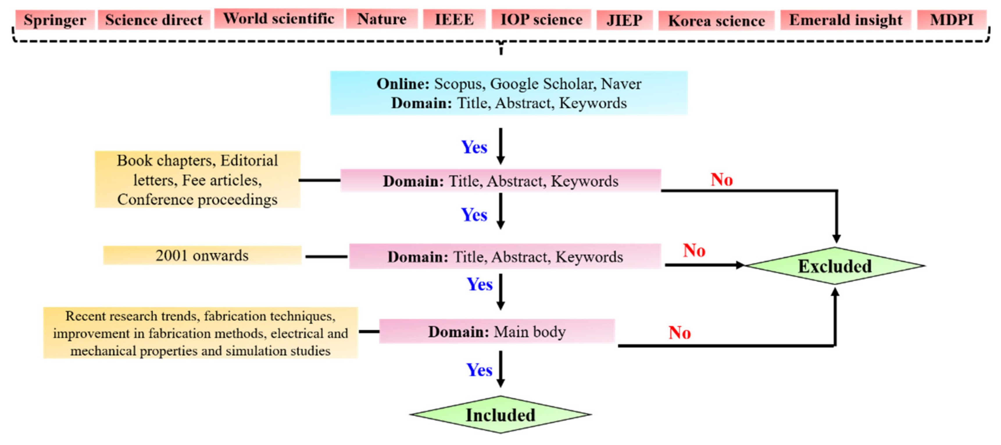
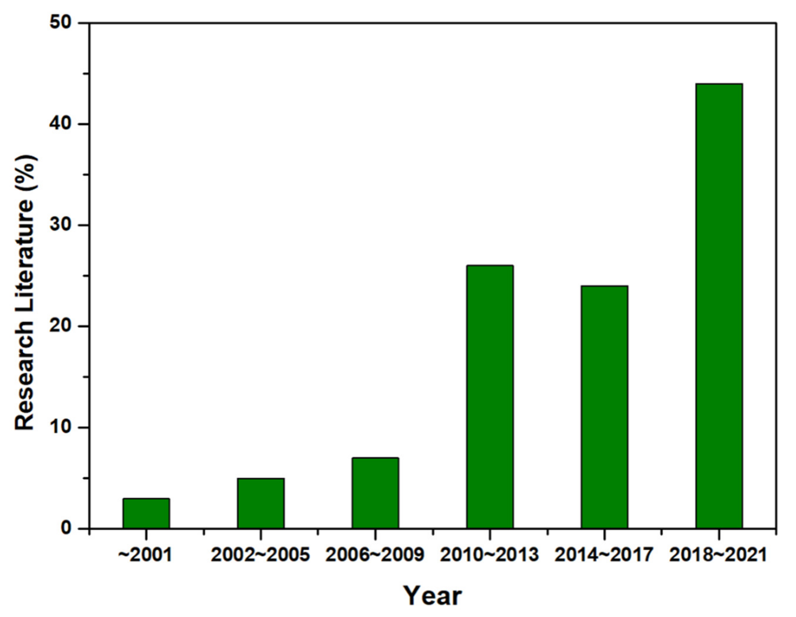
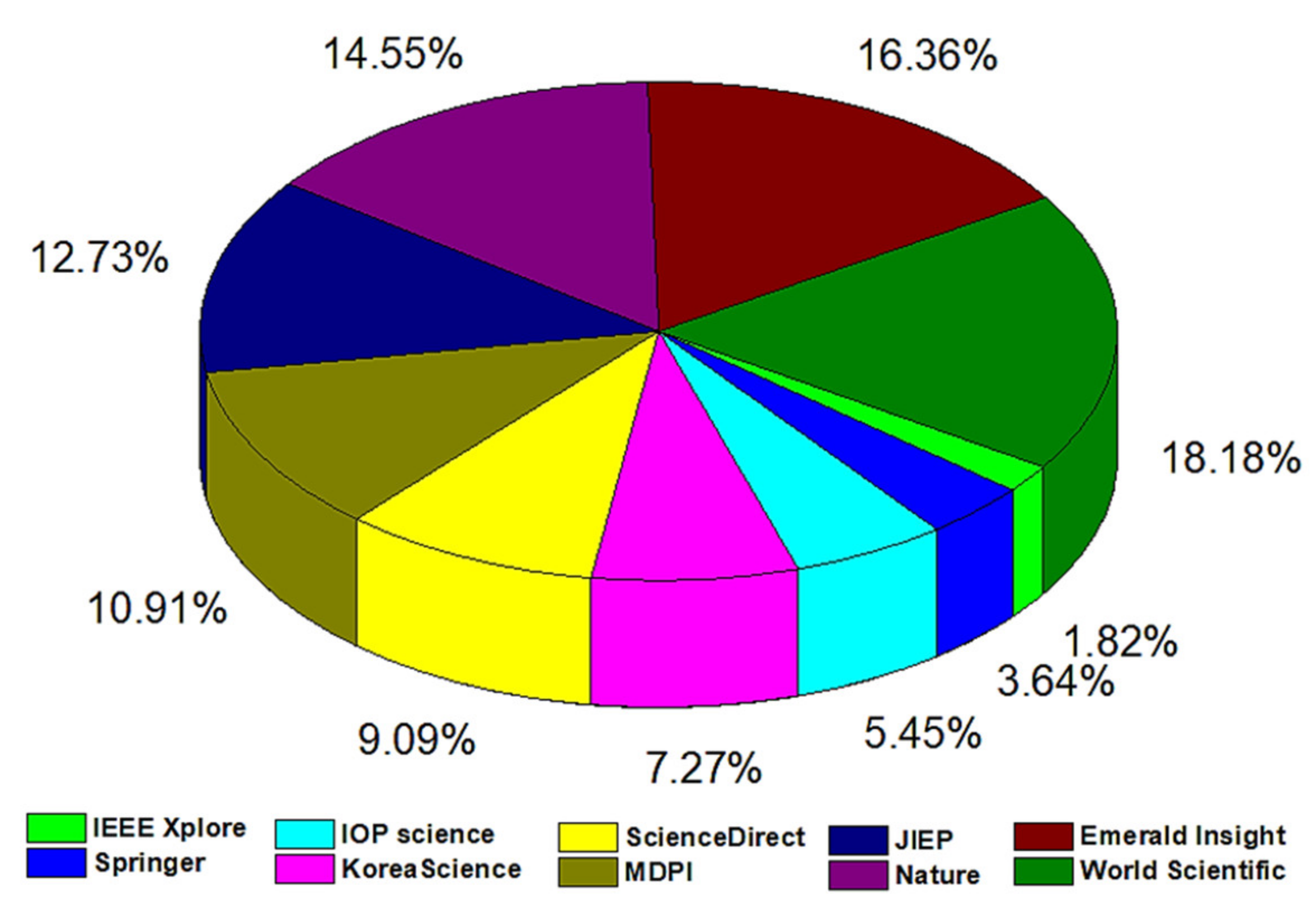
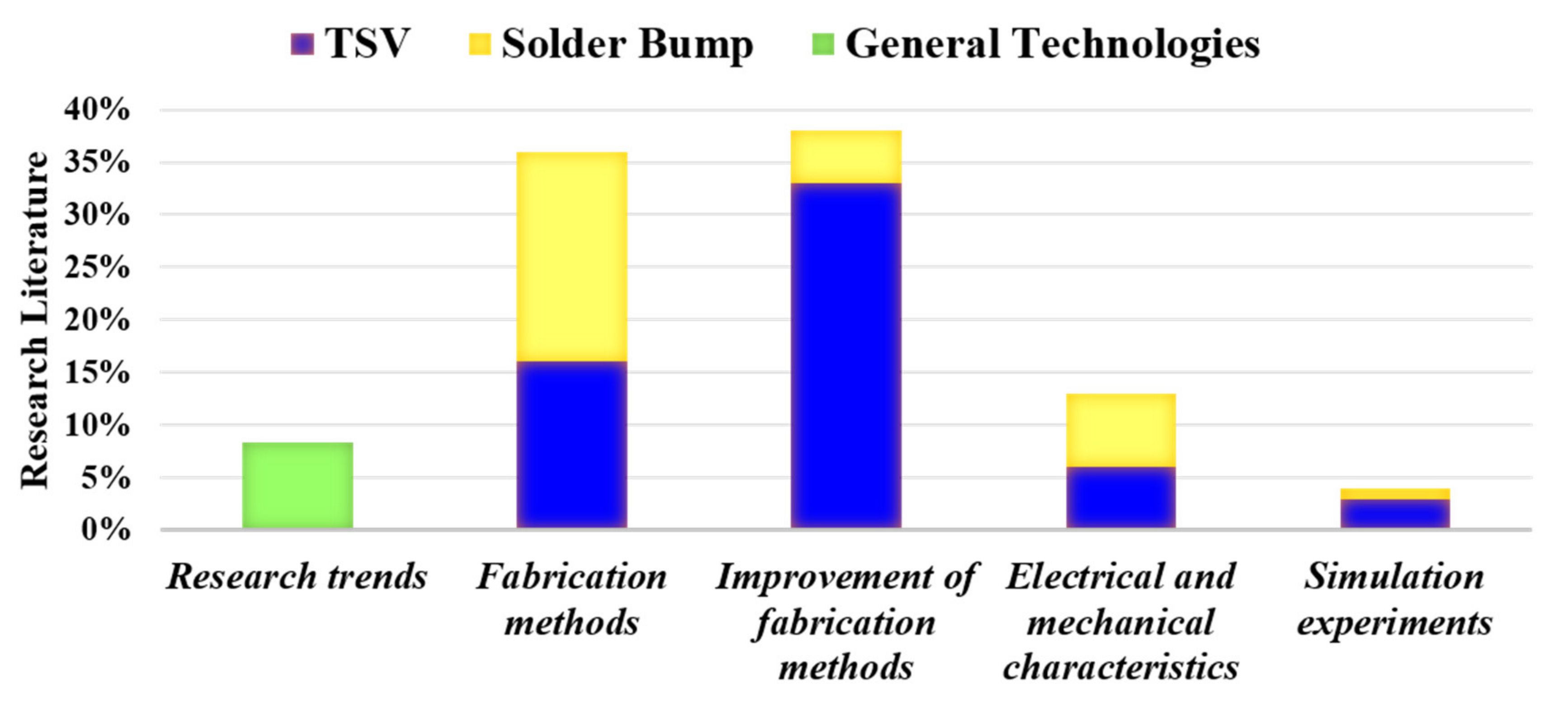
Research Methodology

In this paper, a comprehensive review of 3D interconnection technology is presented. Additionally, the most popular die stacking technologies such as TSV and solder bumping through electroplating are given much attention. In addition, the most recent technologies in bumping such as TSV filling by molten solder, Cu pillar bumping, solder ball bumping, solder injection bumping, solder paste printing, and bumpless joining are studied to get a better understanding of their implementation in the industries and the associated challenges. Figure 1 shows the pictorial representation of acceptance and rejection criteria of the papers included in the present review. The discussion is based on 108 articles in related fields, starting from the year 2001 until 2021. The rest of the references includes patents and the thesis related to TSV and solder bumping. The distribution of research publications from 2001 to 2021 for TSV and solder bumping are shown in Figure 2.
The research articles are directly or indirectly related to TSV, solder bumping, electronic packaging, and the reliability analysis. Academic repositories such as Springer, Science direct, Nature, IEEE Xplore, IOP science, JIEP (The Japan institute of electronic packaging), Korea science, Emerald insight, and MDPI were used to collect the relevant materials. Figure 3 depicts the percentage of journal publications collected from each of the publishers in TSV and solder bumping. The topics such as recent research trends, fabrication techniques, improvement in fabrication methods, electrical and mechanical properties, and simulation studies were covered individually for the TSV and solder bumping parts. The histogram shown in Figure 4 gives the percentage of each research topic associated with TSV and solder bumping.
The main objectives of this research are given below:
  • Collective overview of 3D packaging technologies and their importance in recent microelectronic packaging is introduced.
  • Research trends and challenges associated with the TSV fabrication techniques is discussed systematically, and the important features are highlighted.
  • The electrical and mechanical properties of TSV are analyzed in relation to their fabrication technique, and the future direction to overcome the reliability issues is discussed.
  • Research trends and recent developments associated with solder bumping techniques are reviewed and illustrated pictorially.
  • The advantages and disadvantages of various solder bumping techniques are tabulated with respect to current technological limitations.
  • The future directions to improve the reliability of the solder bumping is discussed in terms of controlling the intermetallic compound at the TSV/solder bumping interface.

2. Through-Si-via

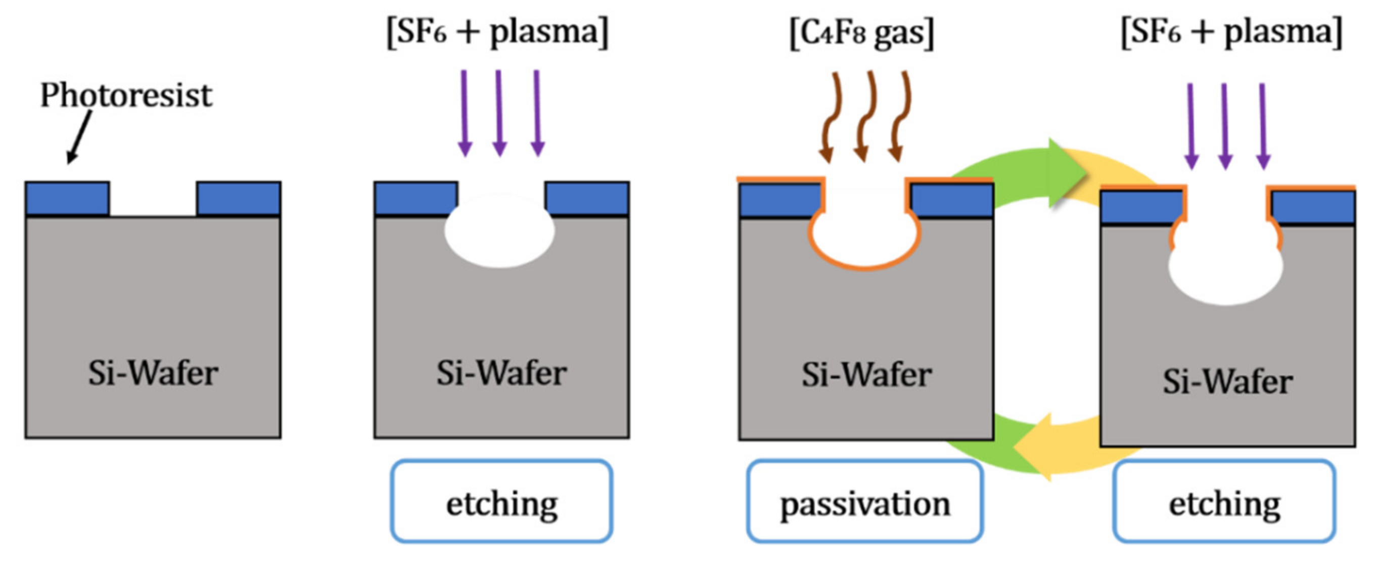
2.1. TSV Formation and DRIE Technology

For forming TSV, the deep reactive ion etching (DRIE) process is generally used. The Bosch process, also known as the DRIE process, can form multiple holes and TSVs with various aspect ratios. The Bosch process was invented by Laermer et al. [17,18], and it is named after Robert Bosch, a German company. The Bosch process has been used to fabricate TSVs by many researchers [19,20]. We explore how a focus exposure matrix can be used to study the motifs encountered on the sides of silicon features etched with the Bosch process. Alternative etching and passivation processes are repeated to achieve vertical via hole. In the reaction chamber, fluoride gases such as SF6, CF4, and C4F8 collide with plasma and change the gas molecules into ions. The etching process is a repetition of silicon etching using reactive ions from SF6 gas passivation of TSV by C4F8, which has similar characteristics to Teflon. The following equations are chemical reactions during etching (Equations (1) and (2)) and protective layer passivation (Equations (3) and (4)) during the Bosch DRIE process [18].
SF 6 + e plasma SF 5 + + F + 2 e
Si solid + 4 F gas SiF 4 gas
C 4 F 8 + e plasma C 3 F 6 + CF 2 + e
nCF 2 ( CF 2 ) n
Figure 5 shows the schematic diagram of the DRIE process. During the DRIE process, due to the etching and passivation process, it forms a scallop shape at the wall of TSV [21]. However, the disadvantage of the scallop shape is that it hinders the formation of the Cu seed layer for Cu electroplating or cause a leakage current that degrades the performance of TSV [22]. Park et al. [23] reduced the average scallop depth by 91% from 230 to 20 nm by optimizing reactive ion etching (RIE) condition of 100W radio-frequency power and 30 SCCM (standard cubic centimeter per minute) of SF8 for 30 min, resulting in smooth profiles of the sidewall trench. Frasca et al. [24] reported that by forming a ‘Michelangelo step’ using 40% concentration of KOH at a temperature of 60 °C, it is possible to prevent scallop formation and perform conformal shape during Cu filling.
The critical aspect ratio phenomenon in DRIE can be controlled using the micro-loading effect and RIE lag [25,26]. The micro-loading effect is the difference in the etch rate depending on the aspect ratio and size of the fine pattern of the TSV structure. Wang et al. [27] showed that the reduction in array pitch increased temperature accumulation and etching speed to suppress micro-loading effects. The RIE lag is when the lower etching rate occurs at smaller feature width [26]. Gerlt et al. [28] have achieved RIE lag reduction by adjusting the two-step Bosch process parameters. With simplicity and adaptability intact, they reduced RIE lag to below 1.5% at an etching depth of 50 μm.
The shape of TSV differs from the ratio of C4F8 gas used for protection layer and SF6 gas used for etching. [29]. If the C4F8 ratio is not appropriate, an oval-shaped TSV is obtained. An oval shape TSV is prone to the closure of the entrance, which makes it easier to form a void or seam inside TSV, as shown in Figure 6. When the ratio of SF6 increases, positive trapezoidal TSV forms. Positive trapezoidal TSV causes the silicon via closing at the top, which hinders the complete filing of TSV. Using a precise ratio of C4F8 and SF6 makes it possible to form the vertical shape of TSV. In the vertical shape, current waveform control can avoid void or seam defects [9,30] or additives into plating solution [31]. However, an unsuitable plating solution and plating condition can cause high current density at the entrance of TSV, which closes the opening and causes voids and seams inside the TSV. To lower the current density at the edge of TSV, rounding of the edge is used. When the ratio of C4F8 is increased, an inverted trapezoidal shape is formed (see Figure 6), and due to its shape, entrance closure during filling is prevented and makes complete TSV filling easier. Roh et al. [32] performed complete Cu filing of tapered TSV with a gradient of 11° and top diameter size of 44.3 μm, bottom diameter size of 34.2 μm, and depth of 60 μm.

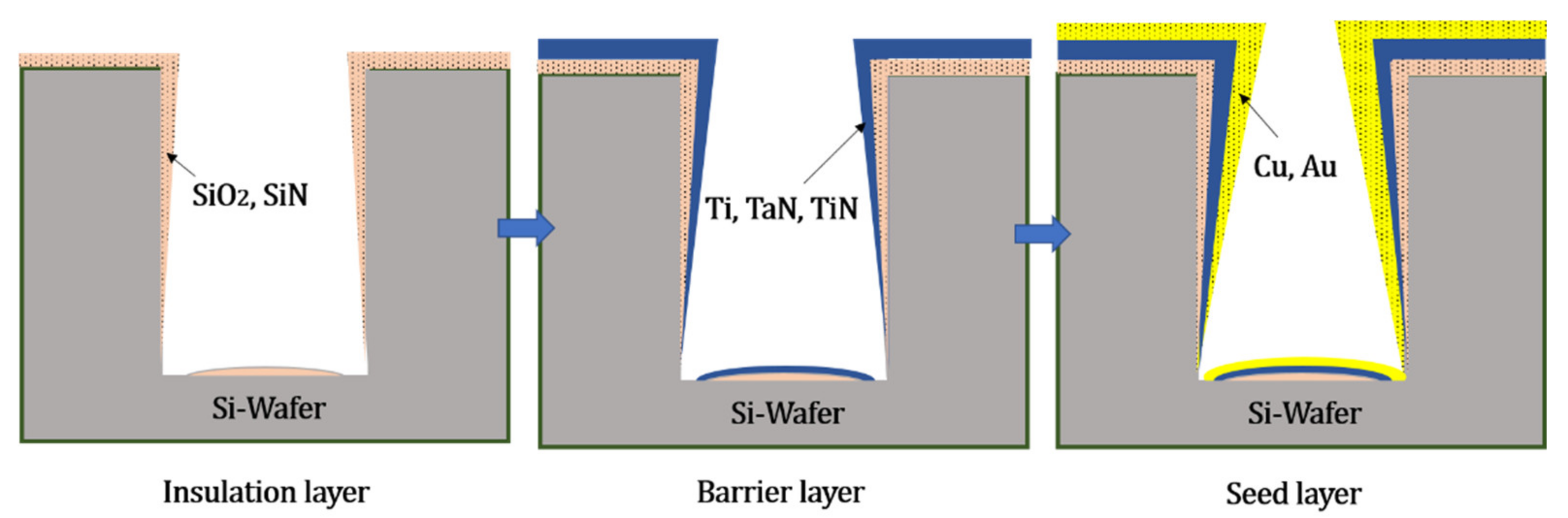
2.2. TSV Inner Wall Coating
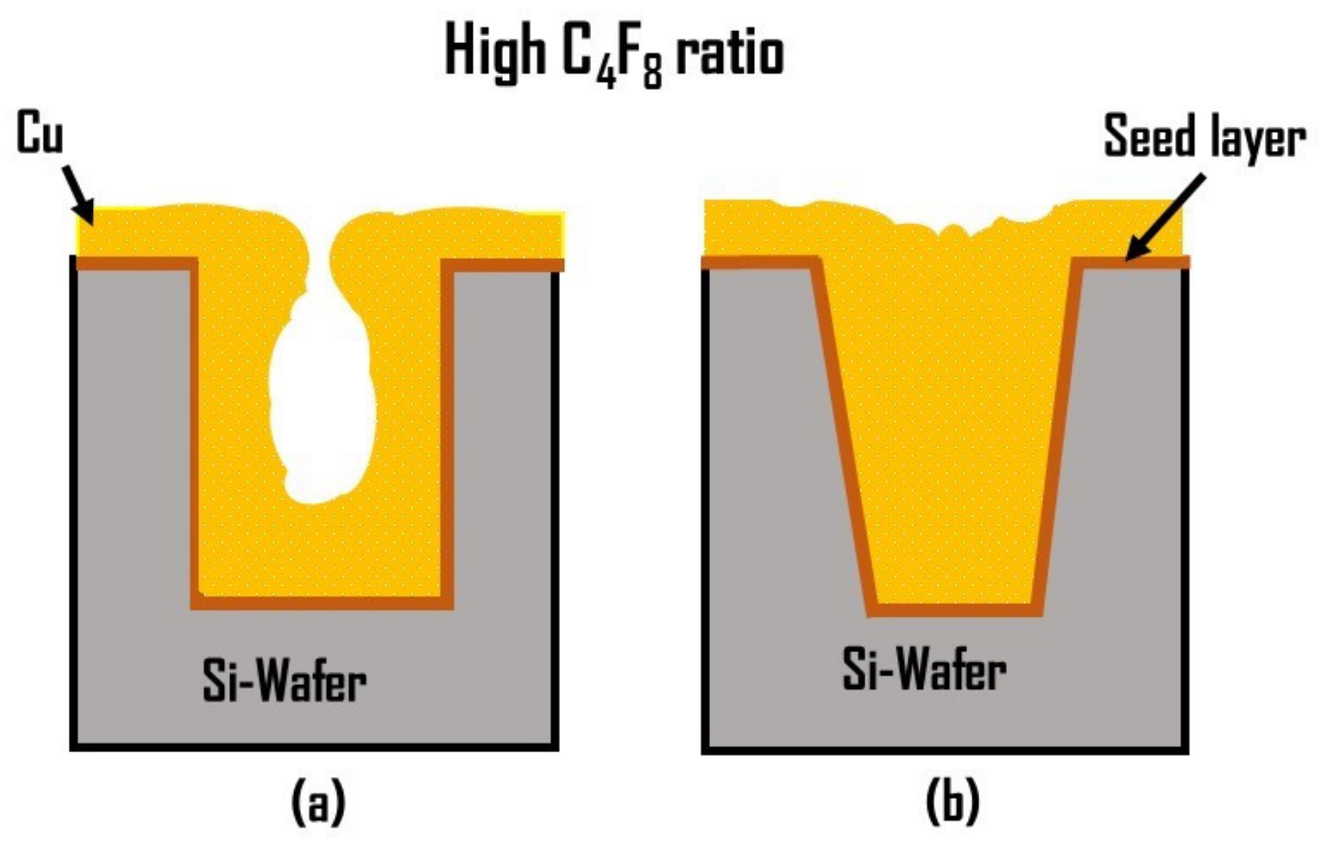
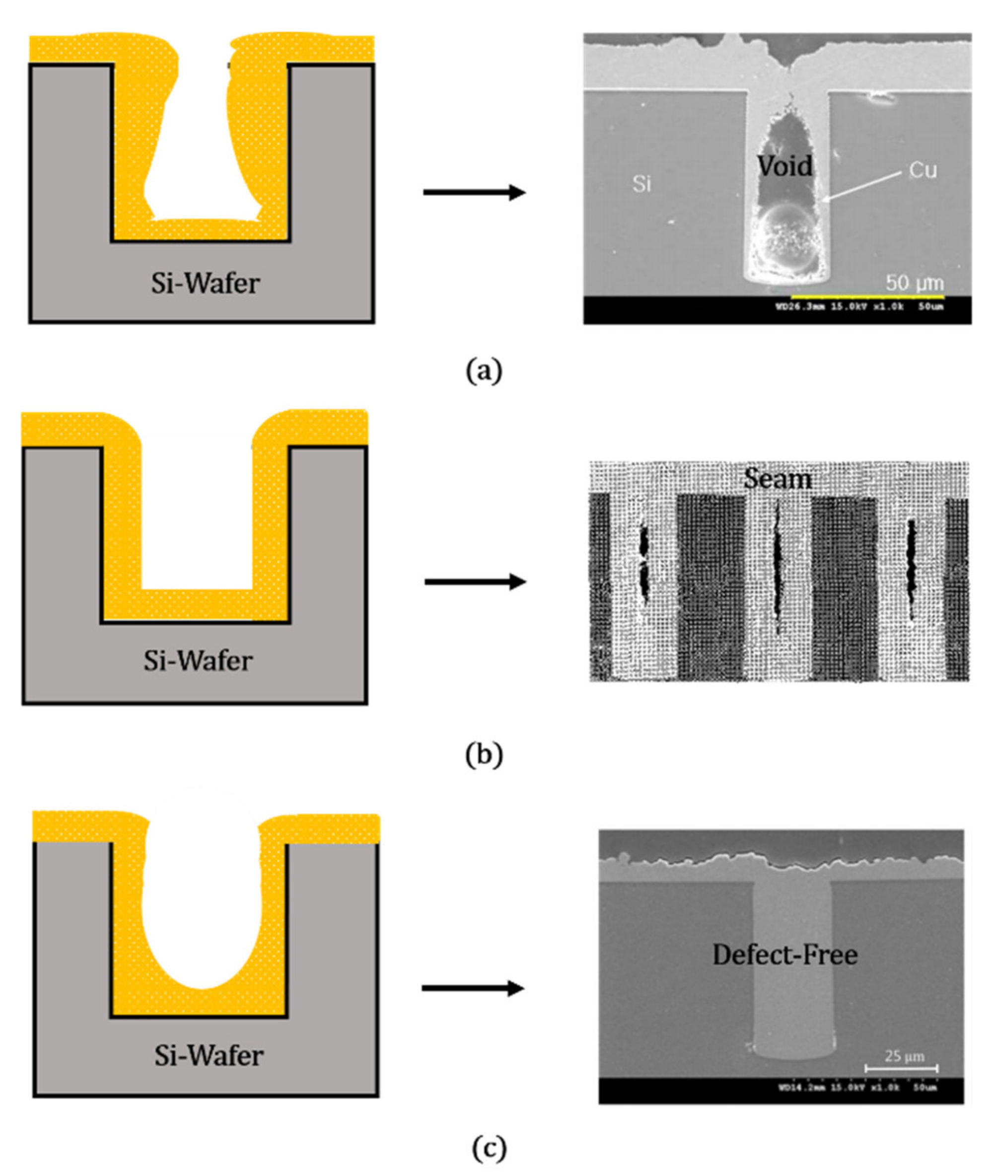
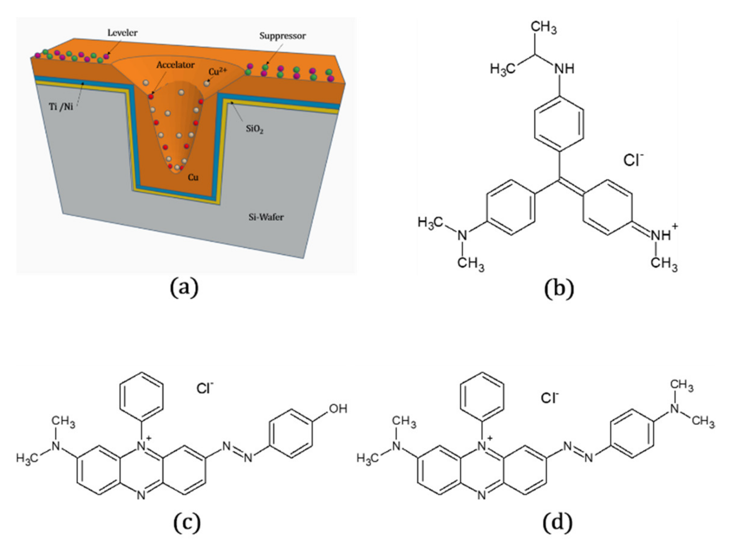
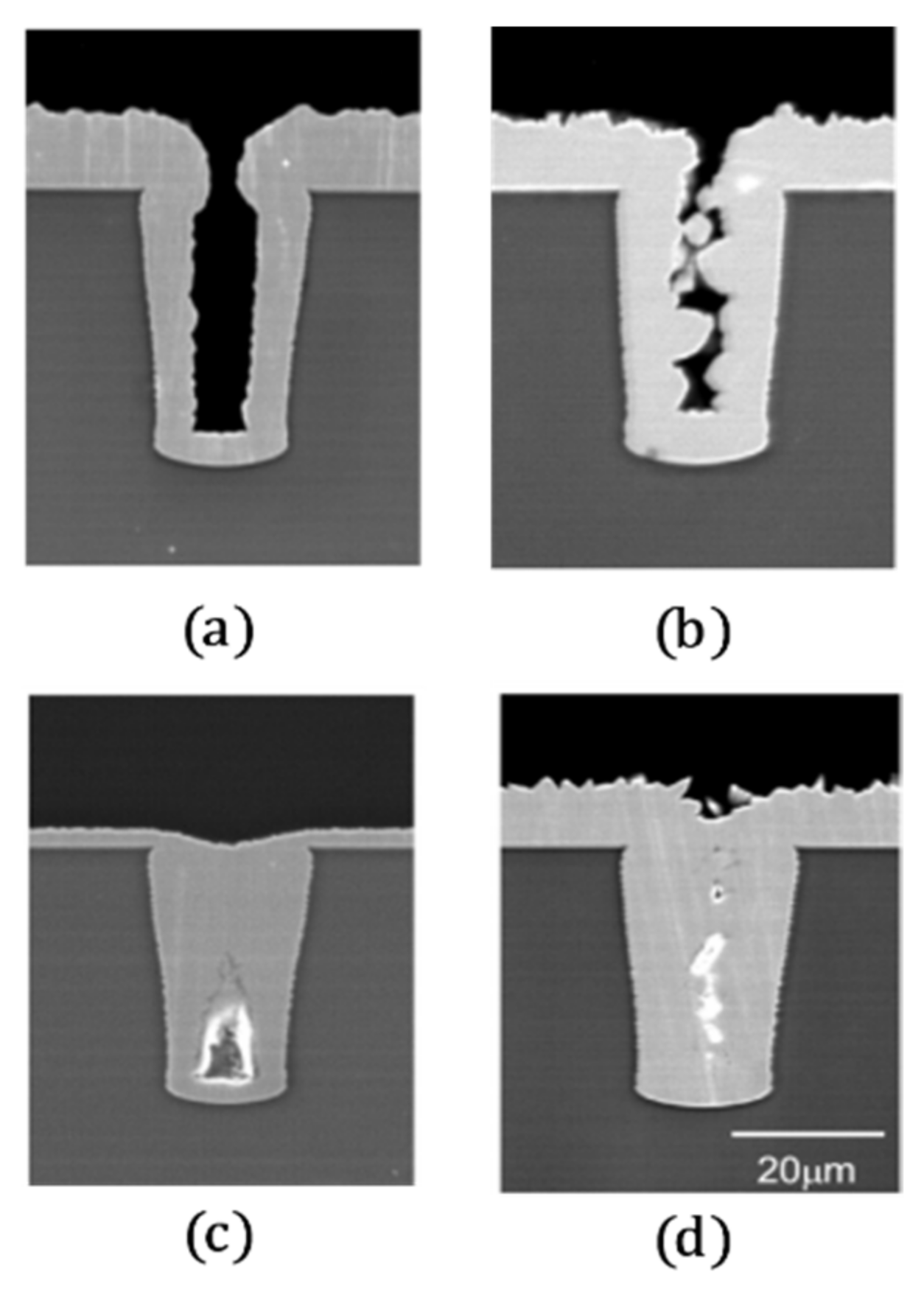
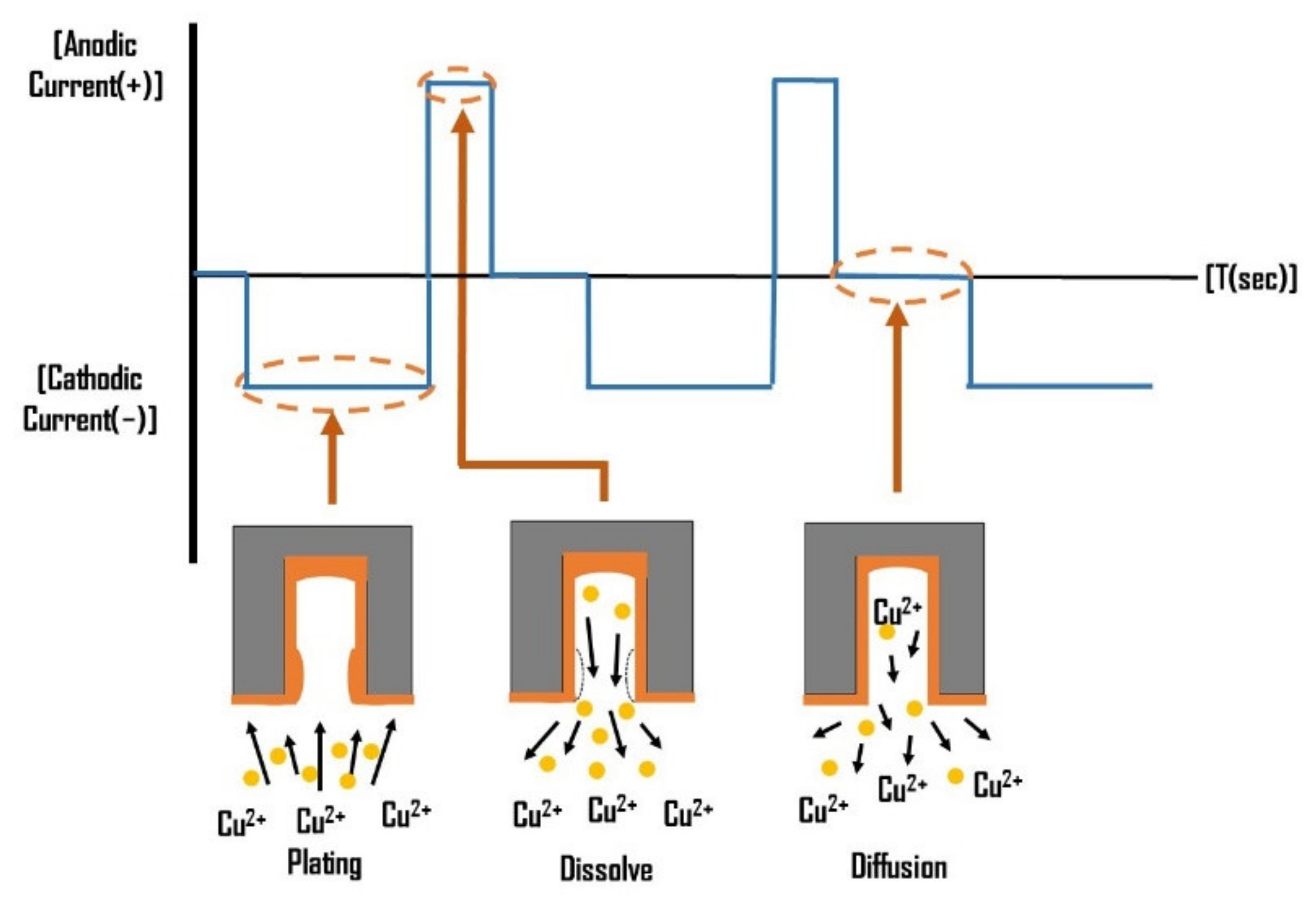
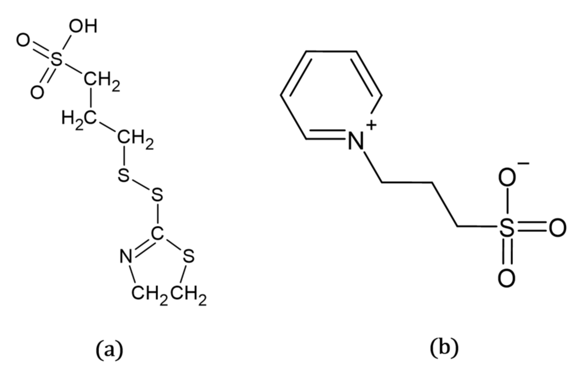
Multiple layers such as an insulating layer, a barrier layer, and a seed layer are coated on the TSV inner wall. SiO2 or SiN are generally used as an insulating layer to form electrical isolation between TSV and the Si wafer. SiO2 can be coated by using chemical vapor deposition (CVD) of SiH4. The chemical reaction formula is given in Equation (5) [8]:
SiH 4 gas + O 2 gas SiO 2 Solid + H 2 gas .
Lin et al. [33] have shown that the wet thermal oxidation method can also be used to produce a SiO2 layer around 1 μm thickness on TSV. Coatings of Ti, TiN, and TaN are used as a barrier layer to improve bonding between the filling metal inside TSV (Cu) and Si wafer and to prevent the diffusion of filler metal into the Si wafer. The thin Ti layer is widely preferred over SiO2, since it has a good joining property to SiO2 and Cu filling material. [10]. Seed layers such as Cu and Au are selected to ease the electroplating of the Cu filler metal in TSV. Generally, the Cu thin film has good conductivity and is widely preferred [34]. Zhang et al. [11] successfully deposited barrier and seed layers in ultra-high TSV using atomic layer deposition and sputtering respectively and subsequently filled Cu in TSV by electroplating. Murugesan et al. [35] used electroless Ni as a seed/barrier layer to TSV with a width of 800 nm and AR of 12 or higher. Ni effectively blocked the thermo-mechanical stress caused by Cu, and when annealed at 300 °C, it also served as a good barrier to Cu diffusion. However, Cu is easy to be oxidized and it can be consumed during Cu electroplating by dissolution into electroplating solution. There is a report of using the Au layer to prevent oxidization and to achieve higher chemical stability [9,36,37]. Hong et al. [9] has coated SiO2, Ti, and Au as protection and seed layers inside the TSV.
Sputtering is generally used to form a thin metal layer of Ti/Cu or Ti/Au over the SiO2 layer. Roh et al. [32] coated 1 μm thick SiO2 using high-density plasma CVD (HDPCVD) and Ti for the adhesion layer and Cu as a seed layer by sputtering [32]. Figure 7 shows the process flow for the forming of functional layers such as insulation, barrier, and seed layers. Kee et al. [38] coated SiO2 (1 μm thick), Ti (0.3 μm thick), and Cu (0.5 μm thick) as insulating, adhesion, and seed layers, respectively in TSV for Cu-SiC filling. Al2O3, TaN, and Ru are adopted as insulation, barrier, and seed layers, respectively, by Knaut et al. [39] with the TSV aspect ratio being higher than 20:1 via a diameter of 5 μm and depth of 110 μm. Generally, the seed layer inside TSV is thick at the entrance of TSV and thin at the bottom of TSV. This happens due to the irregular linear movement of metal atoms during the sputtering process. This causes metal atoms to be more deposited at the entrance of TSV than at the bottom. It is increasingly becoming difficult to conformally deposit barrier and seed layers inside TSV as the aspect ratio increases. An electroless metal (EL) plating process is widely used to form conformal and seed layers. Matsudaira et al. [40] have reported on Co-alloy as a barrier layer. On Pb nanoparticle catalyst, they have electroless plated CoWB and CoB. They have shown that CoWB film that has a larger content of W by 15% had a promising diffusion barrier property. As a result, they have shown that CoWB film with W higher than 15% had a promising diffusion barrier at 350 °C annealing. Murugesan et al. [12,41] have plated a Ni layer using the electroless deposition technique and reported that Ni can act as a good seed layer for the flawless filling of TSV. In addition, by forming an even concentration of Ni ions inside TSV, they have achieved a flawless 10 μm diameter Cu-TSV with a resistance value of 36 mΩ.

2.3. TSV Filling

After coating functional thin films in TSV, conductive metals are filled to TSV. Generally, filling of the metal is done by electroplating, but in the case of TSV with a smaller diameter under 1 μm or trench filling, the electroless plating method can be used [42]. The Si wafer is the cathode during electroplating and as metal ions (ex. Cu2+) receive electrons from the cathode and deposit them inside the via hole.
Cu 2 + + 2 e Cu
The amount of electro-deposited metal is proportional to current, and it can be calculated by Faraday law as shown in Equation (7)
W = ZQ
where W is the amount of metal deposited, Z is the electrochemical equivalent, and Q is the current flow.
The electroplating method is suitable for mass production, and it can produce flawless filling by modifying the current waveform and additives to the plating solution. In addition, using the electroplating method, it is possible to fill TSV with a few μm diameter and a high aspect ratio. Hong et al. [43] have reported the bottom–up Cu-filling method by manipulating the current waveform. However, during the electroplating process, electric current concentrates at the entrance corner of TSV, which is one of the reasons for flaws in the TSV. TSV can categorize into three types—sub-conformal, conformal, and super-conformal—by the shape that TSV is being filled, as shown in Figure 8 [44,45,46]. During sub-conformal formation Figure 8a due to the faster plating speed at the entrance corner of TSV by higher current density, the opening is closed before the internal part of TSV is filled. This causes the formation of a void inside the TSV. During conformal formation Figure 8b, TSV overall is plated at nearly equivalent speed, and this causes a seam inside the TSV. Only by super-conformal formation Figure 8c where faster plating occurs from the bottom of the TSV is flawless filling is possible. Super-conformal formation of TSV has been reported by Hoffmann et al. [47] and the authors [46].
When direct current (DC) is used to fill conductive metals such as copper, the higher current density at the entrance corner of TSV makes it easy to form a sub-conformal shape. To prevent the formation of voids and seams in TSV, the phenomenon of high current density at the entrance of TSV needs to be hindered. The pulse current can be adopted to prevent the formation of defects in TSV. Alternately applying reduction current, which fills TSV, and oxidation current, which dissolves over the coated Cu parts, impedes the early closure of the entrance of TSV. There is a method of setting the oxidation current to 0. However, only by adopting this method, it is a little difficult to avoid the overcoating of Cu [48].
To use pulse current in the plating process, an accelerator, suppressor, and levelers must be present in the plating solution, as shown in Figure 9a. Frequently, bis-(3-sodiumsulfopropyl) disulfide (SPS) is selected as an accelerator, and polyethylene glycol (PEG) is selected as a suppressor [49]. In addition to an accelerator and suppressor, levelers play a crucial role of obtaining the flawless filling of TSV. Organic materials such as Janus Green B (JGB), diazine black (DB), and methylene violet (MV) can be adopted as levelers as shown in Figure 9b. Jung et al. [31] have reported the effect of these levelers on the Cu-filling morphology in TSV, as shown in Figure 10. The authors have achieved defect-less via filling with pulse current and the concentration of each additive to 50 ppm. When MV was added as an additive, it was possible to see the size reduction of the internal defects. In the case of JGB, Cu was not uniformly plated from the entrance to the bottom of the via. When DB was added as an additive, a large-sized void formed at the bottom of the via during filling. Due to small concentration, levelers adhered to the Cu surface by diffusion. As they attached to the entrance edge, they hindered the growth of the plating layer, which improved the via filling quality. Therefore, they can be considered inhibitors, while levelers are essential to achieve flawless via filling.
Electroplating done using pulsed currents had difficulties in getting flawless fillings in the TSV. Lee et al. [46] have reported using periodic pulse reverse (PPR) when filling Cu in TSV. The authors have shown that when the reduction current is −7 to −10 mA/cm2, the oxidation current is 30–50 mA/cm2, and the distance between the anode and cathode is 3 cm, the sub-conformal shape was formed and created defects such as void and seam. Hong et al. [44] have reported that when the mean current density of PPR is −7.71 mA/cm2 and the distance between the anode and cathode is 3 cm, the plating firstly occurred at the middle of TSV, which created a void and seam. It could have happened due to the lack of uniform bottom–up filling, which caused copper to meet somewhere in the middle of TSV.
According to Hong et al. [44], defects that occur by Cu filling by pulse current were reduced by applying the current-off duration between the reduction current and oxidation current, as shown in Figure 11. When using the PPR current waveform for TSV filling, Cu is plated at a reduction current, overcoated metals are dissolved to the plating solution at the oxidation current, and during the current-off period, dissolved Cu ions are diffused in the plating solution. By this process, TSV remains open, which can prevent defects such as voids and seams from forming. There is another improved Cu filing method using the pulse current. Jin et al. [50] have reported that using short a duty time with high frequency could promote bottom–up filling and prevent Cu from growing in the middle of TSV. The report has indicated that with the current density of 2 mA/cm2 and frequency of 4444 Hz, 6 × 60 μm2 size TSV was filled in 30 min.
The pulse current process has the disadvantage of longer filling time due to the plating stage at the reduction current and the etching stage at the oxidation current. Therefore, research focused on shortening the Cu filling time. Firstly, Hong et al. [51] reported that with Cu-Ni alloy as the filling metal and with the PPR current waveform, the filling time was reduced by 1.36 times more than pure Cu filling. In addition, some reports reduced the filling time by changing the suppressor and accelerator in the plating solution. Kim et al. [52] showed that by adding thiourea to the suppressor, PEG-PEG-SPS-I, the filling time is halved. In addition, Sung et al. [53] found out that the reduction in efficiency of the electroplating method occurs when unstable CuI exists at the suppressing layer. To prevent the formation of CuI, they replaced an iodine ion in PEG-PEG-SPS-I to bromine ion and made PEG-PEG-SPS-Br. By using this suppressor material, they halved the filling time. Dinh et al. [54] have suggested a new leveler material, sulfonated diallyl ammonium bromide copolymer (SDDABC) with 16 ppm concentration; they filled 20 × 45 μm TSV in 5 min. It was five times faster than the 1 ppm concentration of SDDABC. Ha et al. [55] achieved the filling time of 3 min by optimizing sulfonated diallyl dimethyl ammonium chloride copolymer (SDDACC).
Some researchers reported on additives in the plating solution to simplify and optimize the Cu-filling process. Shin et al. [56] optimized the concentration of three chemicals: polyethylene glycol (PEG) as a suppressor, bis-3-(sodiumsulfopropyl disulfide) (SPS) as an accelerator, and Janus Green B (JBG) as a leveler. With the optimized concentration and pulse current, they successfully filled Cu in the TSV with various aspect ratios (2, 2.5, 3) with a depth of 60 μm without defects. The on-current density was 10 mA/cm2, and the reverse current density was 16 mA/cm2. The optimized concentration of each chemical was 500 ppm of PEG, 5 ppm of SPS, and 30 ppm of JGB. Wu et al. [57] reported on the interaction between three additives in the plating solution when executing defect-free Cu filling in TSV. When three additives were independently added to the plating solution, they had different inhibition behavior. When they were added together, the interaction varied at different potential values. Tomie et al. [58] have reported that when the suppressor and leveler were added together at the plating solution, even though the suppressor covered the Cu surface, the leveler eventually replaced the suppressor. Therefore, it can be said that the leveler plays a key role when executing bottom–up Cu filling in TSV. The reports stated have added three chemicals: a suppressor, leveler, and accelerator in the plating solution to perform defect-free Cu filling. However, using three chemicals simultaneously is challenging. To successfully use three chemicals at once, understanding each chemical and the data of the optimized concentration of chemicals are needed. Therefore, to improve the efficiency and simplify the Cu-filling process, some researchers reported using a single additive to the plating solution. Wang et al. [59] have reported by using single inhibitor material, 3-(2-(4,5-dihydrothiazol-2-yl)disulfanyl)propane–1-sulfonic acid (SH110) shown in Figure 12a, they were able to perform defect-free Cu filling at the current density of 1 mA/cm2. Le et al. [60] suggested another additive material of 3-(1-pyridinio)-1-propanesulfonate (PPS), as shown in Figure 12b; using the current density of 0.2 A/dm2 and 5 g/L concentration of PPS, they successfully filled the TSV with Cu.
Recently, researchers improved the filling ratio and filling speed by applying ultrasonic vibration during Cu filling in TSV. Xiao et al. [61] were able to electroplate Cu to TSV with a high aspect ratio depth (20 × 200 μm2) with 105 W ultrasonic in 5 h and achieved the filling ratio of 98.5%. Wang et al. [62] experimented with variables such as the concentration of accelerator, electric current density, and the existence of ultrasonic. As a result, of ultrasonic, the filling ratio improved by 23% and was able to fill 20 × 60 μm2 size TSV in 180 min. Zeng et al. [63] also reported good filling of 20 × 60 μm2 size TSV with no defects in 150 min by applying ultrasonic and pulse current.

2.4. Electrical Properties of TSV

Since TSV is used in various forms depending on the requirement of the chip, it is necessary to study the shape, stacking method, and arrangement structure, which are the variables that can affect the electrical characteristics of TSV [64,65]. Jeong et al. [66] have compared the impedance values for different TSV shapes such as cylindrical, square, elliptical, and triangular shapes. The authors used a four-point probe measurement method to analyze electrical measurement by passing a current through both ends of an unknown resistor and measuring the voltage. The square TSV shape has better electrical performance at high frequency and shows less impedance reduction than other shapes. This is because the quadrangular TSV shape has a higher insulating layer due to its large outer area and protects the signal more than other shapes. For a single Si substrate, Pak et al. [67] modeled the electrical characteristics of TSV based on the number of stacked TSV, their aspect ratio, and the wall layer thickness. The authors reported an increase in total resistance and capacitance with increasing the number of stacked TSVs. The increase in total resistance and capacitance of stacked layers depends on the width and height of TSV. The total resistance can be reduced by decreasing the aspect ratio of TSV, and the total capacitance can be reduced by enlarging the TSV pitch and thickness of the SiO2 layer [67]. Belaid et al. [68] have proposed a model and computed the time-domain coupling noise in the 3D-integrated circuit. They have used the numerical inversion Laplace transform (NILT) method and chain matrices. The authors show that TSV noise coupling is affected by different factors such as source characteristics, horizontal interconnections, and the type of input and output (I/O) drivers.

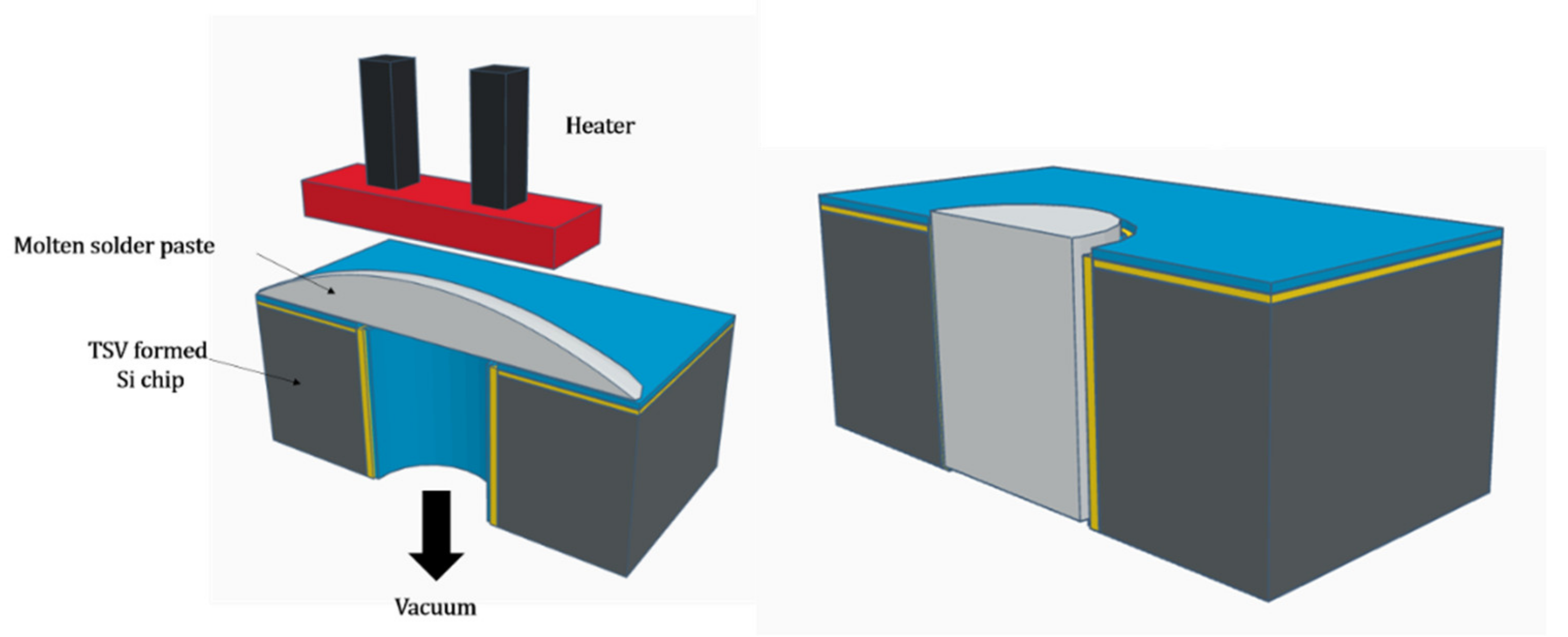
2.5. TSV Filling with Molten Solder

Filling molten solder into TSV is a recent and low-cost via filling technique. In this process, TSV is filled with lead-free solder with a melting point of around 200–230 °C instead of electroplated copper. Molten solder can be filled by the Injection Molded Solder (IMS) or vacuum-assisted via the filling process [69]. In the vacuum-assisted process, by using a pressure of 0.02–0.08 MPa, TSV can be filled with the molten solder by pressure differences between the upper and lower side of the Si wafer, as shown in Figure 13. The solder filling time into TSVs with a diameter of 30 μm and depth of 200 μm was less than 4 s. The solder filling process is faster and easier than the Cu-filling process. However, it has drawbacks such as lower electrical conductivity, electromigration resistance, and lower thermal resistance than Cu-filled TSV.

2.6. Reliability of TSV and Future Directions

Cu must be filled in TSV without any defects for reliable interconnections. Imperfections such as protrusions, voids, seams (shown in Figure 6; Figure 7), etc. can seriously affect the TSV characteristics. The Cu protrusion that appears during the annealing treatment of TSV affects the reliability of TSV. Protruded Cu can cause stress between the Si wafer and Cu-plated layer due to the thermal expansion coefficient (CTE) difference between Si and Cu. It could create cracks, which reduced the lifetime of the chips. Some researchers suggested methods to prevent this phenomenon. Jung et al. [70] have replaced Cu filling with Cu-Ni alloy on TSV with a size of 30 μm diameter and 60 μm of depth. They have shown a reduction of Cu protrusion compared to pure Cu filling from 1360 to 1250 nm (8.8% reduction) at the annealing condition of 450 °C. Roh et al. [32] electroplated Cu-W instead of pure Cu on tapered-shape TSV (entrance diameter 44 μm, bottom diameter 34 μm, depth 60 μm) and showed a 44% reduction of protrusion at annealing condition of 450 °C. Sung et al. [13] have reported a protrusion-hindering effect of additives 2-mercapto-5-benzimidazole sulfonic acid (2M5S) and thiourea at the annealing condition of 400 °C. They have experimented TSV with a diameter of 5 μm and depth of 60 μm. The 2M5S has reduced the Cu protrusion by 84.9% due to the benzene ring in the material. However, 2M5S has created an unstable compound of Cu (I)-2M5S during plating that reduced the uniformity of TSV. Thiourea has hindered the protrusion of Cu by 69.2%. Jin et al. [50] have shown that a short duty cycle and high frequency of 2222 Hz on TSV with a size of 6 μm diameter and 60 μm depth reduces the Cu protrusion by 21.17% at an annealing condition of 430 °C.
Si and Cu filled in vias induce complex internal stresses due to the CTE difference. The internal stress can lead to Cu extrusion from the via and delamination, thereby degrading the reliability of the TSV interconnection. The stress and plasticity behavior of Cu and the as-plated microstructure play an important role in the extrusion failure. TSVs undergoing thermal annealing post-plating exhibited linear elastic behavior without an increase in residual stress [2]. The delamination of Cu from Si is an important reliability failure, as it reduces the electrical signal transfer in stacked dies. It can be controlled by decreasing the TSV diameter or by reducing the CTE mismatch between the Si and Cu [2]. The addition of nanoparticles proved to be beneficial in reducing the CTE mismatch and internal stress between Si and Cu. However, nanoparticles should have good electrical conductivity to improve the transfer of electrical signals. In that case, a CNT (carbon nanotube) has good electrical conductivity and mechanical property in nano dimensions. Sable et al. [71] reported that Cu–CNT-filled TSV with graphene nanoribbons (GNR) as interconnects improved the performance of 3D ICs. The electrical resistance is 57.3% and 72.9% in the case of a copper–CNT composite and copper, respectively. The CNT/GNR interface and copper–CNT/GNR interface offer 80.5% and 64.2% lower interface resistance than their copper counterpart. It can be considered that as for lower radius, the resistance provided is high for all three materials. Chen et al. [72] investigated the fabrication of a CNT–Cu composite using a TSV interposer to secure the high electrical conductivity of Cu and the low coefficient of thermal expansion (CTE) of CNTs. The Cu–CNT pillar inserted to TSV showed electrical conductivity (≈2.5 × 10⁵ S/cm, ≈1/2 of Cu) and CTE (≈7 × 10⁻⁶/K) values equivalent to pure Cu and Si, respectively. The calculated CTE values in accordance with Equation (8) agreed well with the measured value of ≈ 6.2 × 10⁻⁶/K.
α Cu CNT = α Cu K Cu φ Cu + α CNT K CNT φ CNT K Cu φ Cu + K CNT φ CNT
where αCu and αCNT are the CTE of Cu and CNT, respectively, KCu and KCNT are the bulk moduli of Cu and CNT, respectively, and φCu and φCNT are the volumetric fraction of Cu and CNT, respectively. Lwo et al. [73] studied the reliability of TSV under various environmental conditions and analyzed using Weibull analysis. Bias current and thermal cycling were found to be decisive factors affecting the reliability of TSV. In the biased samples, voids were formed at the current corner in the TSV. Apart from that, other reliability failures occurred due to oxidation, delamination, and flanking. Jeong et al. [66] studied the protrusion and stress distribution for various TSV shapes using finite element analysis. It was found that multilayer TSVs have less reliability and higher cracks due to high-stress levels brought by the interaction between multilayers in contact. In addition, the cylindrical and quadrangular TSV shapes displayed high mechanical reliability when compared with the elliptical and triangular TSV shapes. Presently, the factors affecting the reliability such as TSV shape and filling materials are well-established, whereas research on TSV fabrication with nanoparticle addition is rare. Considering the importance of different nanoparticles in reducing the CTE between the Cu filling and Si wafer, research should focus on incorporating nanoparticles in TSV and their effect on the electrical and mechanical properties.

3. Solder Bumping

Solder bumping is the development of a small solder bump on the Cu-filled TSV. Several processes have been demonstrated to develop a solder bump on the TSV successfully. These include electroplating [14], solder ball bumping [15], solder paste printing [5], vapor deposition [74], and injection molding solder of a controlled collapse chip connection new process (C4NP) [75]. The choice of the processes is influenced by the pitch size, production costs, and assembly. Each method has its own advantages and drawbacks. Electroplating has remained the preferred choice because of its low cost, mass production, and importantly, it can be applied to fabricate fine-pitch solder bumps through precise patterning. In electroplating, fine-pitch bumps can be achieved through the precise control of current density and additives. However, an electroplating bath is often prone to varying composition, and proper bath recycling is required before disposal. Solder ball bumping is an eco-friendly process. However, mounting a tiny solder ball for fine-pitch I/O connections requires an expensive assembly setup [15]. Solder paste printing is cost-effective and can be used for mass production. However, flux contamination is an unavoidable issue and affects long-term reliability [5]. Vapor deposition techniques such as evaporation and sputtering can provide a uniform composition solder bump, but the process is expensive [74]. Solder bump is the most widely used soldering technology in ball grid arrays (BGA) and flip-chip technology. In the present review, the important characteristics of solder bumping related to fine-pitch TSV interconnections are discussed.

3.1. Solder Bump by Electroplating

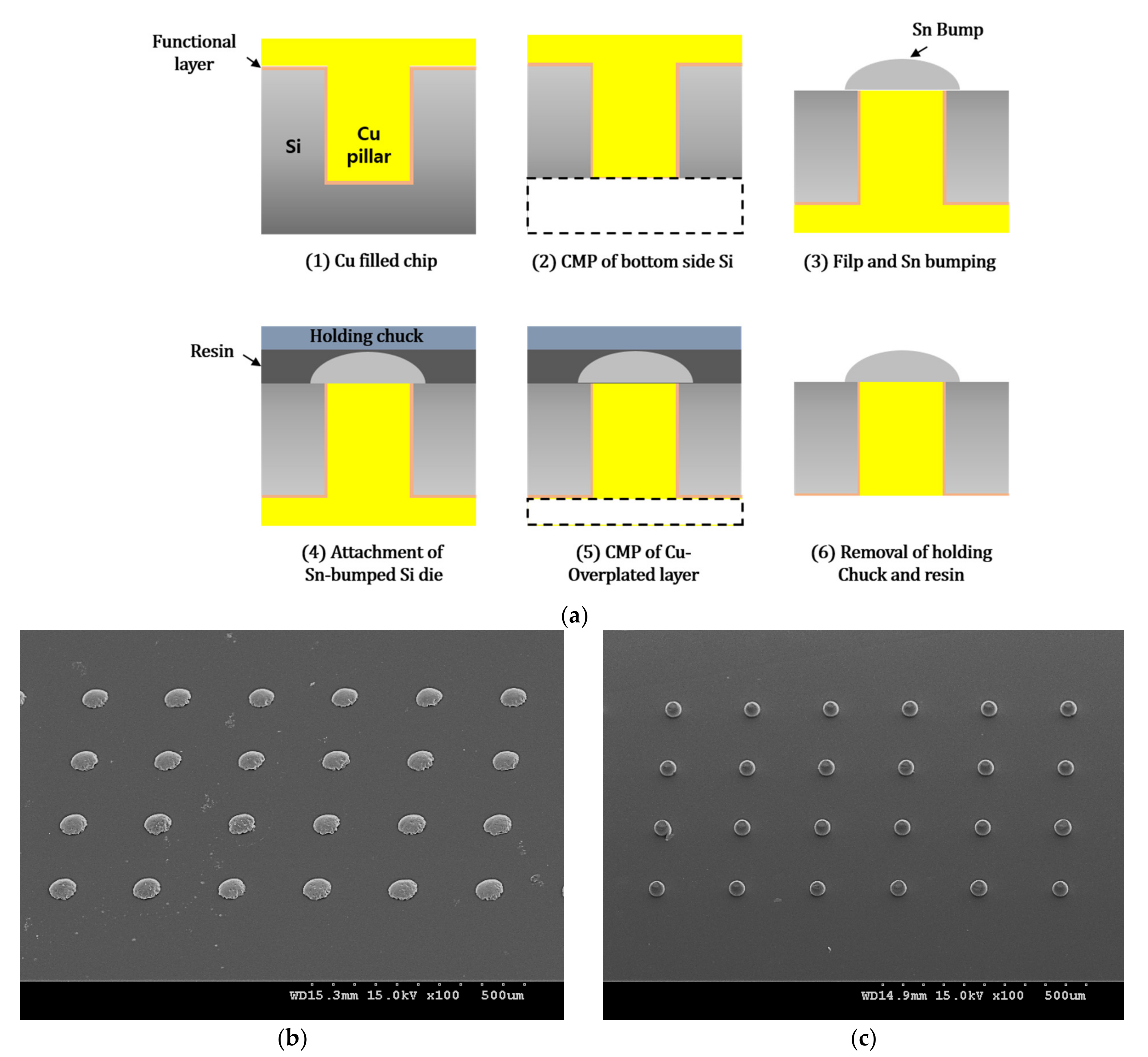
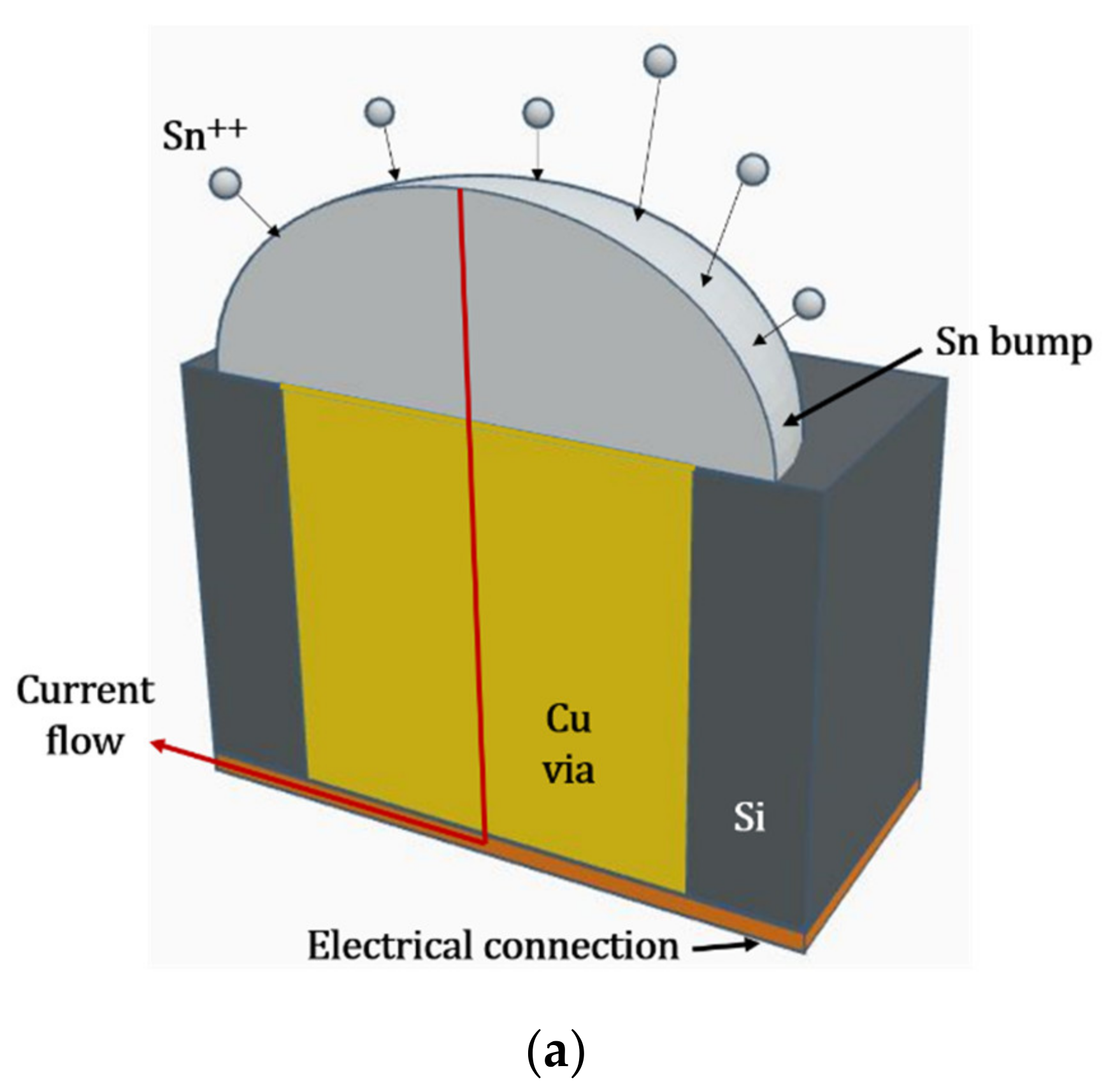
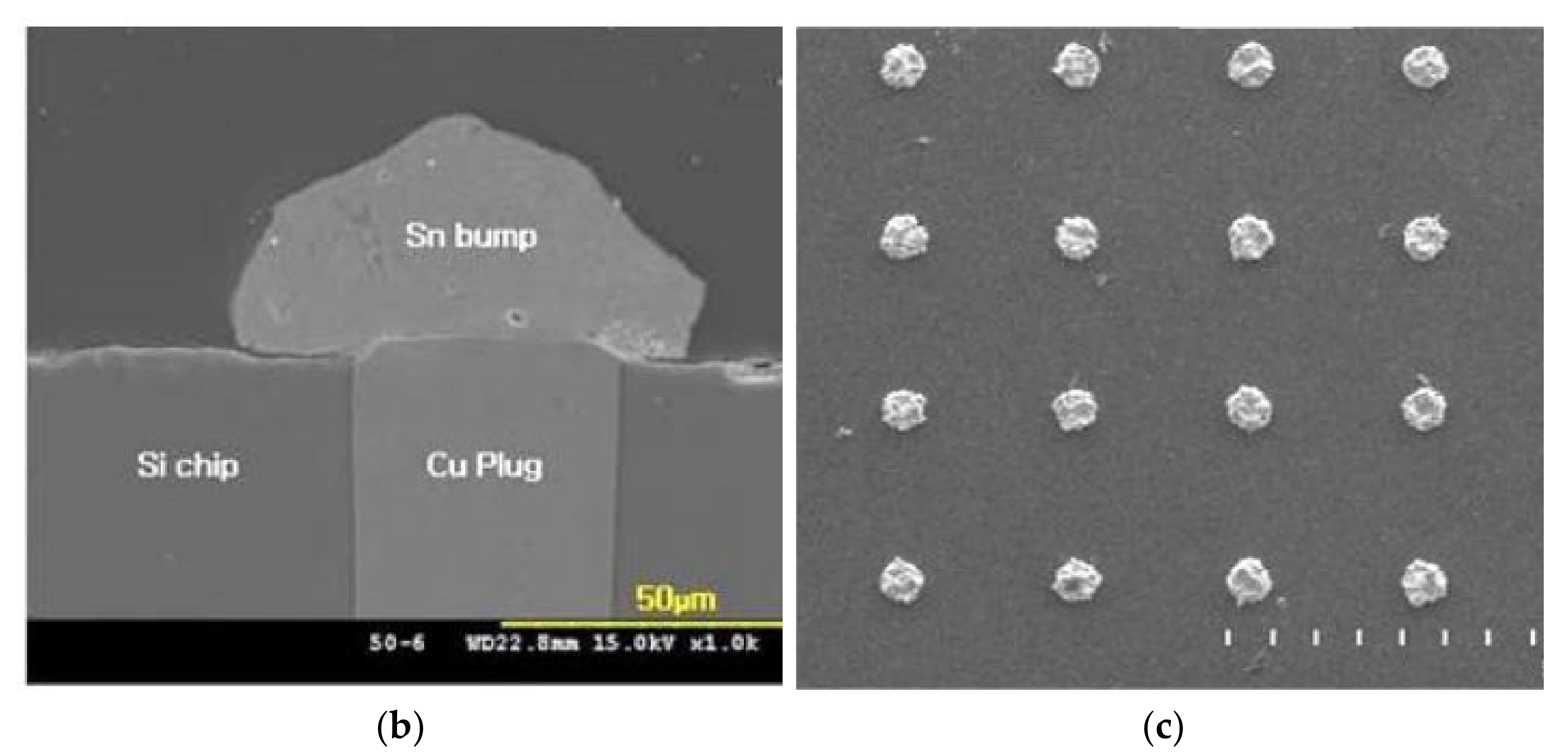
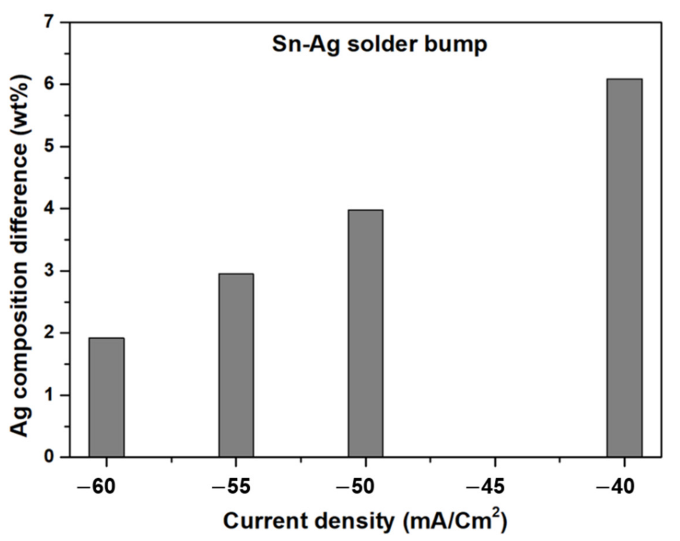
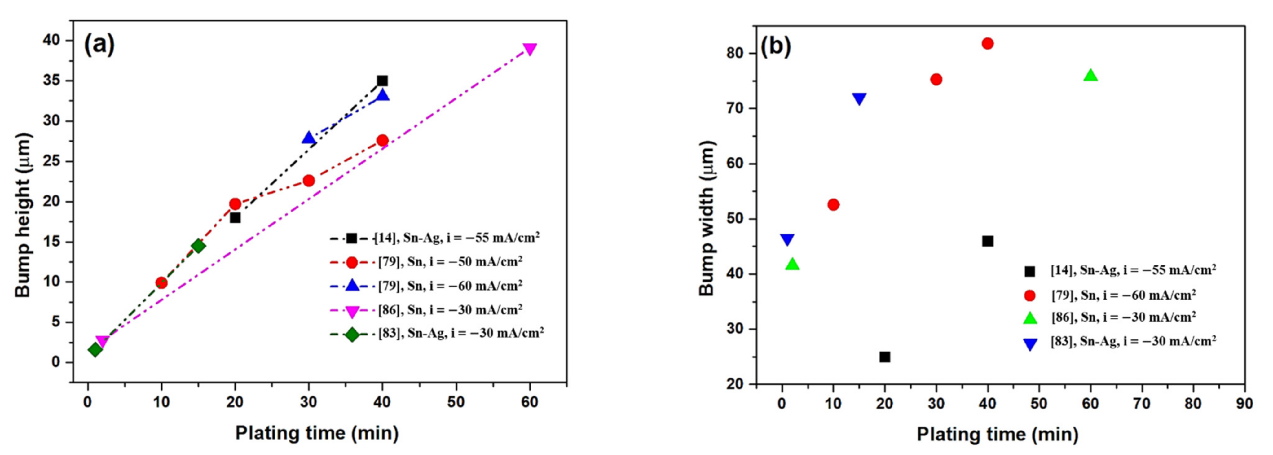
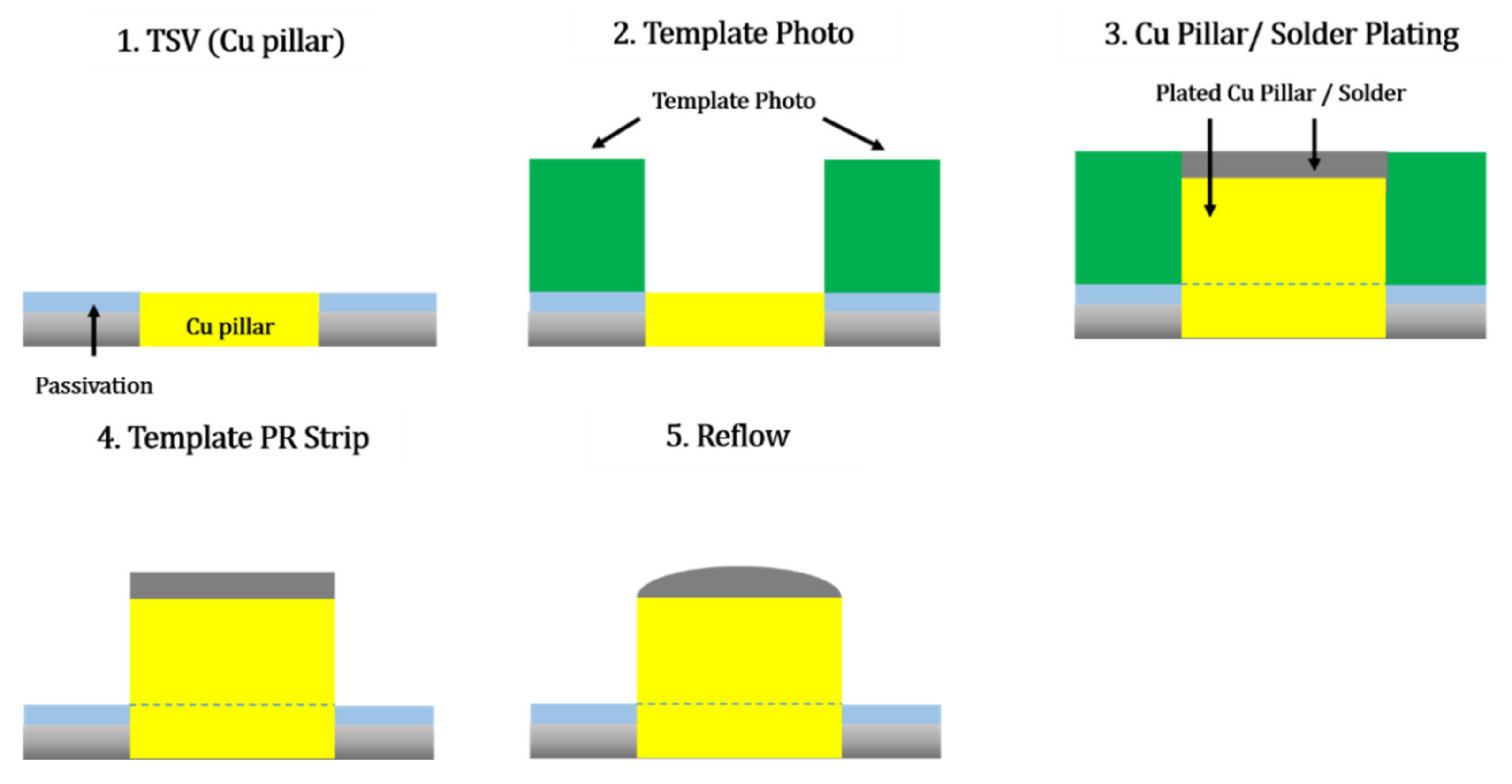
3.1.1. Solder Bump Plating on TSV

Sharma et al. [14] successfully electroplated Sn-3.5 Ag solder bumps on the Cu-filled TSV from an acidic electroplating bath composed of SnSO4, H2SO4, Ag2SO4, thiourea, and some additives. The eutectic composition was obtained for a plating time of 40 min and a current density of −55 mA/cm2. The plated solder bump was reflowed at 260 °C for 20 s. The reflowed Sn-3.5 Ag solder bump was a spherical shape with a dimension of ≈35 × 46 µm. The shear strength test results show that shear strength rises from 75 to 110 MPa with increasing shear speeds from 0.5 to 10 mm/s. However, higher shear speed decreased the shear strength and resulted in a brittle intermetallic (IMC) fracture mode.
For the 3D stacking of silicon chips, a solder bump is formed on a Cu-plug in TSV, which connects every Cu-filled TSV electrically and mechanically with upper or lower TSVs. In this case, it is important to control the bump size to achieve desirable stacking. Hence, during electroplating, a photoresist (PR) is generally used on Si to control the exact bump size [76]. The bumping with a PR mold consists of lithography processes such as PR coating on a wafer, film masking, UV lightening, patterning, and PR stripping to produce a PR mold. Tanida et al. [77] obtained a tiny sized bump with fine pitch using a PR mold. Sn or solder capping on the Cu-plug in TSV can also be adopted to keep a gap between the Si chip and avoid bridging a solder between the neighboring solder. Meanwhile, a bumping process on a Cu-plug without a lithography process (non-PR mold) to reduce the cost and number of steps is shown in Figure 14a. Using this process, Sn- and Sn-Ag bumps were produced on the Cu-TSV [78].
Figure 14a shows process steps for bumps formed on the Cu plugs by DC electroplating without the PR mold. For electroplating conditions, −55 mA/cm2 current density, and 30 min time, Sn-3.5Ag solder bumps were successfully plated using the non-PR bumping Figure 14b,c. The solder is a low alpha solder of Sn-3.5Ag, which emits low alpha radiation particles. The as-plated solder bump diameter is around 50 μm, and after reflow, the hemispherical bump diameter became approximately 30 μm. However, the deposition of a non-PR bump depends on the uniformity of TSV. For instance, defects in TSV such as seam, cavity, or incomplete filling of Cu in TSV results in irregular solder bumps based on the defect type. Figure 15 shows the appearance of irregular and non-uniform Sn-3.5 wt % Ag bumps formed on the Cu plug in TSV having 30 μm in diameter and 60 um in depth. The plating condition was −55 mA/cm2 current density for 20 min by the non-PR bumping method. It is attributed to the non-uniform Cu filling height in the TSV and results in the poor bonding during TSV stacking [44].
Hong et al. [36] successfully fabricated Sn bumps on Cu plugs in TSVs using a simplified process without any serious defects. Cu was electroplated and filled in via holes without PR, where the lithography process is not used for Sn bumping. In this process, a Cu plug is exposed on one side of Si surface where a Sn bump will be produced by electroplating. The other Si surface side is coated by a seed metal such as Cu or Au to supply current for Sn bumping through a Cu plug in TSV, as shown schematically in Figure 16a. Sn bumps were formed by DC current electroplating with a current density of 3 A/dm2 for 15 min. The Cu plug diameter in TSV is 35 μm, and the Sn bump diameter in the bump bottom is 64 μm. In another study by Hong et al. [36], decreasing the current density of DC to 0.05 A/cm2 and increasing the plating time for 30 min, Sn bumps about 22 μm in height and 68 μm in diameter were produced by the DC plating, and the bump was similar to a mushroom head shape without a columnar part. The bump surface was relatively facet-rich, but it was not connected with the neighbor ones. The size of the bump is primarily uniform, and none of the bumps showed serious defects, as shown in Figure 16b. Bumping without the lithography method has advantages such as omitting the following steps: PR (photoresist) coating, film masking, UV (ultraviolet) exposure, patterning, and PR stripping processes [76,80]. The author also uses the non-PR process in various studies [9,78,79].
The standard equilibrium potential of Ag is more positive than that of Sn. Hence, during electroplating, precise control in plating current density and time is required to achieve a uniform composition throughout the solder bump [81]. A Sn–3.55 wt % Ag solder bump with a height and diameter of 18 and 92 μm, respectively, was obtained by electroplating at a current density of −55 mA/cm2 for 20 min [9]. During the electrodeposition of Sn-3.5Ag on a Cu-filled TSV, the circumferential edge part on top of TSV deposited more preferentially than the center part of TSV, because the current density along the edge is higher than the center part of TSV [82]. Figure 17 shows the difference in Ag composition deposited at the top and bottom of the bump for different current densities. The compositional difference decreased by varying the current density from −40 to −60 mA/cm2. In addition, it was observed that the Ag content at the bottom of the Sn–Ag bump is generally higher than that at the top. Since the Ag ion is nobler than Sn and deposited at a lower current density, Ag is deposited earlier than Sn [83].
The electroplating thickness is dependent on the plating current density and time and can be expressed using Equation (9) [82]:
X = E c i ε t 60 ρ
where X is the deposition thickness, t is the electroplating time, Ec is the electrochemical equivalent of the deposit, i is the current density, ε is the cathodic current efficiency, and ρ is the deposit density. In Sn-3.5Ag bumping, using Equation (9), Jun et al. [83] reported the cathodic current efficiency (ε) for the Sn-3.5Ag bump as 45.05% [Ec = 0.04358494 g/C, i = 30 mA/cm2, ρ = 7.412 g/cm3 for Sn-3.5Ag].
Park et al. [84] studied the Sn-Cu solder bump height variation by increasing the deposition time from 1 to 35 min for a current density ranging from 1 to 5 A/dm2. The plating rate of the near-eutectic Sn-Cu bump increased linearly from 0.27 to 2.28 μm/min by increasing the current density from 1 to 5 A/dm2. For a constant plating time of 10 min, the bump height increased 10 times from 2.3 to 21.9 μm by increasing the current density up to 5 A/dm2. The theoretical bump height was calculated using Equation (10) [84]:
h = A wt nF i ad t
where Awt is the atomic weight, n is the number of electrons, F is the Faraday constant, i is the current density, t is the deposition time, a is the plated surface area, and d is the deposit density. From Equation (10), it is clear that the bump height is directly proportional to the current density and deposition time. However, in reality, other factors might deviate the bump height from the linear dependence in (10). It is confirmed by comparing the theoretical and the experimental bump height for varying time and current density. The linear increase in bump height is observed only up to a current density of 4 A/dm2, after which the bump height remains constant. In addition, the maximum plating efficiency is obtained for 3 A/dm2. Similarly, for a constant current density of 1 A/dm2, a linear increase in bump height is observed up to 25 min plating time. Unlike the theoretical results, for further increases in plating time, the bump height remained constant. This shows that optimizing the electroplating factors such as current density and time is important to obtain the maximum efficient solder bump. Similar studies were carried out for Sn and Sn-Ag solder bumps [3,4,5,6,7,8,9,10,11,12,13,14,15,16,17,18,19,20,21,22,23,24,25,26,27,28,29,30,31,32,33,34,35,36,37,38,39,40,41,42,43,44,45,46,47,48,49,50,51,52,53,54,55,56,57,58,59,60,61,62,63,64,65,66,67,68,69,70,71,72,73,74,75,76,77,78,79,80,81,82,83,84,85,86]. For all the bumps, the bump height and width increased with increased plating time, as shown in Figure 18a and b respectively. Similarly, in Sn-Cu bumping, by electroplating in the condition of 2.5 A/dm2 for 10 min, bumps 20 × 20 × 10 μm3 in size with 50 μm of bump pitch were formed [84]. A near eutectic Sn–0.72 wt % Cu bump was produced in the plating condition of a reduction current density of 1 A/dm2 for 23 min. Hence, the precise optimization of plating current and time is necessary to obtain the solder bump of desired dimensions.
For fine pitch electrodes, a Cu pillar with the electroplated solder method is the most popular. However, the electroplating of a solder bump on the Cu plug in TSV has some drawbacks. For example, the plating solder composition is practically limited to dual systems such as Sn-Ag and Sn-Cu. Plating thickness is varied depending on the wafer position. Maintenance of plating solution, condition, and equipment is quite complicated, and investment cost is relatively high.

3.1.2. Cu Pillar Bump with Solder Cap

Micro-bumping is important for the vertical connection of stacked chips in 3D electronic packaging, including TSV technology. When the micro solder bumps are formed on TSV by the electrolytic plating method, the pitch between the bumps usually has a range of 70–140 μm. However, for smaller pitch size < 70 μm, there is a possibility of connections (bridging) between neighboring solder bumps during reflow. In order to improve this problem, Cu Pillar Bump (CPB) technology was introduced. The schematic illustration of the CPB process is shown in Figure 19.
In CPB, a higher Cu bump is formed on TSV by electrolytic plating, and a thin solder film is plated directly on the top of the Cu bump [87]. In CPB, a finer pitch can be achieved without bridging [88,89]. Ma et al. [90] fabricated an ultra-fine pitch bump consisting of a 6 μm Cu pillar, a 0.5 μm Ni layer, and a 5 μm Sn layer on the top of the Cu pillar that was produced by electroplating on the Si die with a photoresist mold. The diameter of CPB micro-bumps was 20–7 μm, and the micro-bumps were reflowed at 230 °C for 80 s. After aging treatment at 190 °C, they found that Cu3Sn was formed around the Cu pillar sidewall. The growth rate of the Cu3Sn sidewall increased with the decrease in micro-bump diameter. The growth rate of the Cu3Sn sidewall is given in (11):
d IMC = d 0 + K t 1 / 2
where dIMC and d0 are the thickness of IMC, t is the thermal treatment hours, and k is the growth rate constant.
From the experimental results, the growth rate constants of sidewall Cu3Sn were calculated as 0.066 μm2/h1/2, 1.237 μm2/h1/2, and 2.641 μm2/h1/2 respectively for 20 μm, 10 μm, and 7 μm diameter solder bumps. Similarly, Koh et al. [88] fabricated ultra-fine pitch bumps of 30 μm diameter using CPB. In addition, due to the higher joint gap in CPB, excellent heat dissipation and excellent electrical and thermal conductivity and high mechanical yield strength can be achieved.
Tanida et al. [77] also achieved 20 μm pitch using CPB in 10 μm sq. TSVs, namely a Cu bump with 10.4 μm sq. and 5 μm height, and they electroplated a 1.5 μm thick Sn-2.5Ag solder film on the top of the Cu bump. Multilayered IMCs of Cu6Sn5 and Cu3Sn and a single layer of Cu3Sn were formed at the interface at the bonding temperatures of 240 °C and 350 °C, respectively. Lee et al. [87], fabricated a Cu pillar bump capped with Sn-Ag by electroplating for bonding chip stacking with TSV. The size of the micro-bumps was 10 and 20 μm. SiC nanoparticle composite solder was filled into TSV instead of Cu for low-cost and high-speed filing. The addition of 1.0 wt % SiC nanoparticles showed a lower CTE value of 15.0 ppm/°C, which is expected to reduce delamination from the TSV wall.

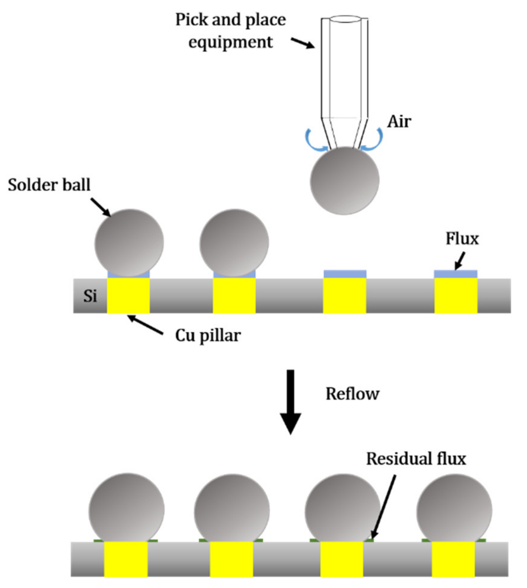
3.2. Solder Ball Bumping

Micro-ball bumping of Sn-Ag and Sn-Cu-Ag solder on the TSV by the pick and place process is shown schematically in Figure 20. It is the most cost-effective process of establishing solder bumps on TSV. It has advantages such as enabling the various sizes of solder bumps and various compositions of solder balls such as Sn-Ag, Sn-Ag-Cu, and Sn-Cu. However, a well-precise assembly setup is required to pick and place the micro solder balls on a fine-pitch Si chip.
Jung et al. [91] reported Sn3.5Ag solder ball bumping on a Cu-filled TSV having dimensions of 60 μm diameter and 120 μm depth. A low-alpha Sn-1Ag-0.5Cu (SAC105) solder ball of diameter 80 μm was placed on the Cu-filled TSV and reflowed at 245 °C peak temperature for 10 s. Low alpha solder is helpful to avoid soft error in high-density electronics and semiconductor packaging. After reflow, at the interface between Cu in TSV and solder bumps intermetallic compounds of Cu6Sn5 were produced. The interfacial IMC of Cu6Sn5 in low alpha solder is similar to that of ordinary solder, and its thickness was 1.71 μm and 4.05 μm before and after aging at 85°C for 150 h, respectively.
Khorramdel et al. [5] used solder paste jetting technology to form a solder ball on the TSV. The authors studied the possibility of developing solder balls directly on the top of TSV to facilitate a finer pitch between the solder ball and an increased density of the I/O connections. The solder ball formation was performed by ink-jetting technology, and jetting solder was Sn-Ag-Cu solder paste. The diameter of jetted solder ball was 227 μm, and to form a ball connection, the solder paste was reflowed at 230 °C. The authors reported that solder paste jetting can be used for pad sizes as small as 200 μm and pitch sizes as small as under 350 μm, which results in four times higher I/O density than the conventional approach while retaining identical TSV dimensions. The reliability of the TSV interposers was investigated by a temperature cycling stress test (−40 °C to +125 °C). Electrical testing up to 1000 cycles did not cause any open circuits or significantly affect the electrical resistance.
In solder ball bumping, flux is used during the solder ball reflow to prevent oxidation. Extreme care should be given during the reflow because the activation of flux can change the alignment of the solder balls and result in a bump to bump bridging during the reflow.

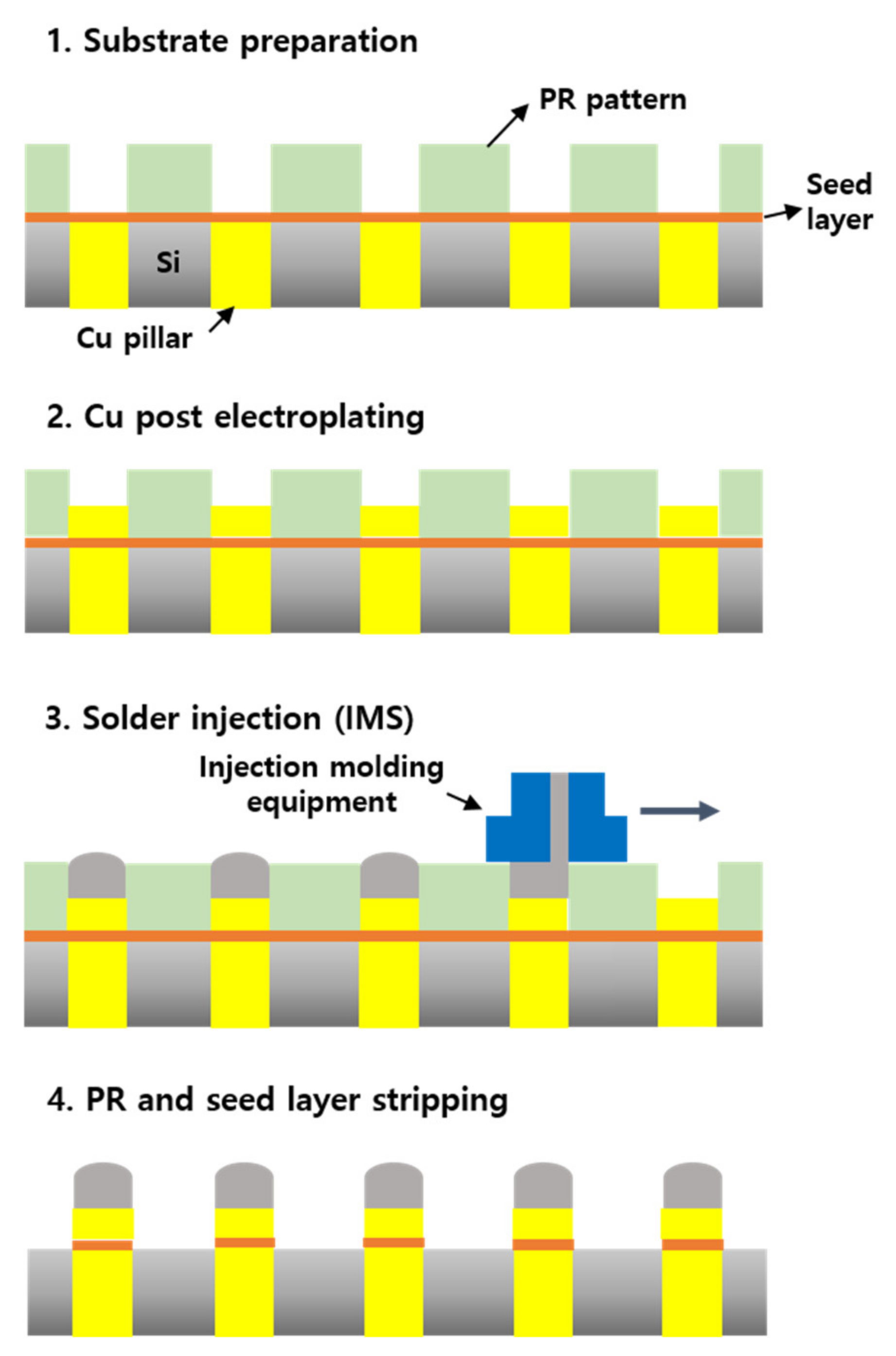
3.3. Solder Injection on Cu-Pillar

The process of solder injection on Cu-pillar, also named injection molded solder (IMS). In this process, molten solder metal is squeezed out from the nozzle tip on the Cu-pillar. [92,93]. This IMS process consists of the following steps: 1. seed layer preparation and photoresist patterning on a Si wafer, 2. Cu pillar (post) plating, 3. solder bumping by IMS, 4. photoresist & seed layer stripping [92]. The schematic illustration is shown in Figure 21.
The advantage of the IMS process can be that a ternary system solder such as Sn-Ag-Cu can be easily supplied. The process is simple, and the bump size is independent of wafer location compared to electroplating. In addition, it is a flux-less process, and solder bumps of various sizes can be formed. The disadvantage is that high-temperature PR is needed because it acts as a dam for the molten solder reservoir until solidification.

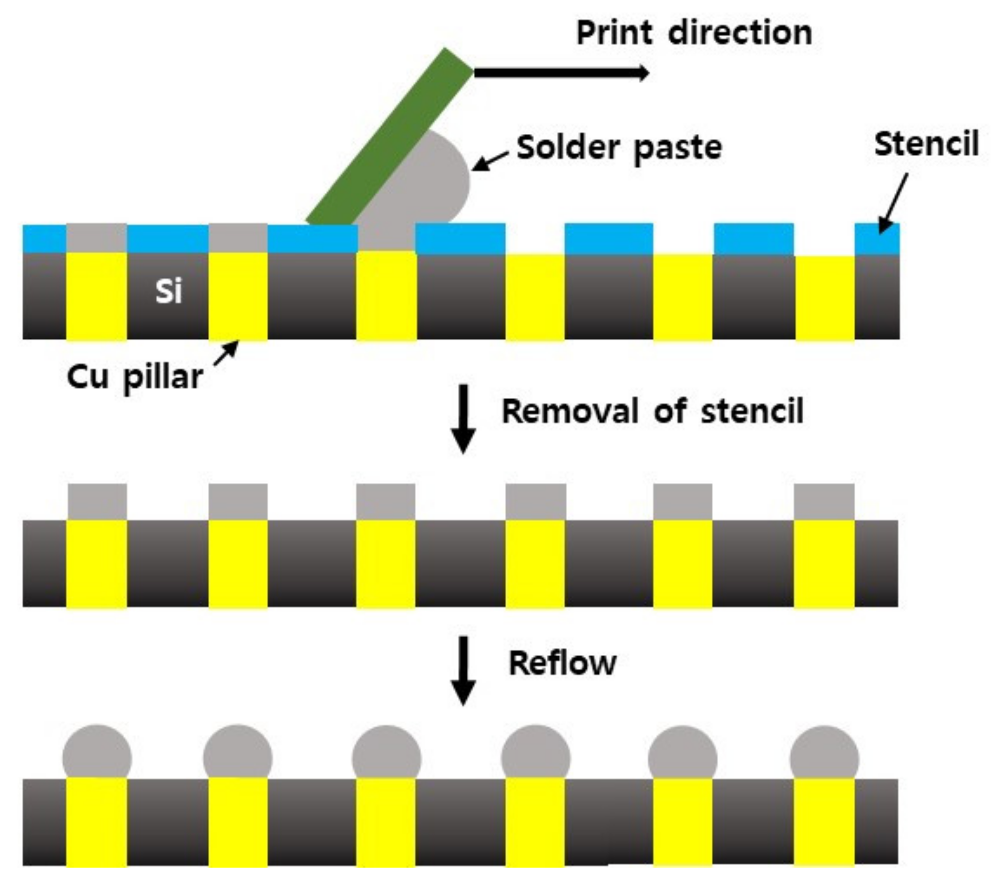
3.4. Solder Paste Printing

In this process, a solder bump is formed by printing solder paste on TSV using a fine-pitch stencil followed by reflow. The process flow for solder paste printing on a TSV is schematically illustrated in Figure 22. In paste printing, various parameters such as the surface condition of substrates, the substrate–stencil ratio (stencil opening size, pitch size, stencil thickness), the printing speed, and the pressure need specific attention to successfully perform paste printing and solder bump formation [94].
Generally, paste printing was not used for ultra-fine pitch TSV substrates. However, recent laser edge technologies for ultra-fine pitch stencil and type-7 solder paste have eased the solder paste-printing process in 3D ICs. In addition, paste printing has beneficial aspects such as simplification of the manufacture process and cost-effectiveness. Today, research is focused on solder paste printing for ultra-fine pitch interconnects. Kim et al. [95] succeeded in bonding a flip-chip scale package with a Cu pillar and solder bump. Optimization studies showed that appropriate printing could be achieved for type-5 and type-7 solder paste for a metal mask having a thickness of 30 μm and 50 μm, respectively, and an opening ratio of 70%. In addition, decreasing the mask thickness to 30 μm and increasing the opening ratio to 100% resulted in a fitting print for type 7 solder paste. The solder bump is successfully formed by printing type-7 SAC 305 solder paste on a substrate with a width of 150 μm using a metal mask with a thickness of 30 μm. Similarly, a wafer-level bump was achieved with type 7 SAC 305 solder paste using the paste-printing process by Kumar et al. [96]. A 100 μm sized solder bump was fabricated using a Ni-Co stencil having an opening and pitch size of 30 μm and 120 μm, respectively. The design of experiments (DOE) approach was used to study the optimum printing parameters. For defect-free printing, the optimum squeeze pressure and print speed was found to be 7 kg and 20 mm/s. Finally, the advantages and disadvantages associated with the various solder bumping processes are summarized in Table 1.

3.5. Reliability of Solder Bump and Future Directions

Solder bump reliability is dependent on the type of the solder alloy system and the IMC formed at the interface. Solder ball bumping, solder injection, and paste printing processes offer solder alloy flexibility on TSV. Although the Sn3.0Ag0.5Cu (SAC 305) system is the standard lead-free solder used in bumping, other systems such as Sn58Bi and Sn57.6Bi0.4Ag are widely used for low-temperature bumping. Depiver et al. [97] studied the fatigue life of Sn37Pb, SAC 305, Sn3.8Ag0.7Cu (SAC 387), Sn3.9Ag0.6Cu (SAC 396), and Sn4.0Ag, 0.5Cu (SAC 405) solder bumps on Cu substrates. The authors reported the highest and lowest fatigue life in the SAC 405 and SAC 387 compositions, respectively. It shows that even a small change in composition in the SnAgCu eutectic system has a significant effect on reliability. The bonding of stacked TSVs and solder bumps is achieved by reflow of the solder bumps. After reflow, the reliability of the solder bump mainly depends on the microstructure and the Cu-Sn IMC formed at the interface. The metallurgical reaction of Cu and Sn results in the formation of Cu6Sn5 and Cu3Sn IMC at the solder bump/Cu pillar interface. After reflow, Cu6Sn5 is formed in accordance with the reactions (12) and (13) [98]:
6 Cu + 5 Sn Cu 6 Sn 5
2 Cu 3 Sn + 3 Sn Cu 6 Sn 5 .
Under thermal conditions, due to the solid-state diffusion of Sn and Cu, the growth of Cu6Sn5 IMC increases. However, Ni atoms substitute the Cu atom in the Cu6Sn5 lattice and form (Cu, Ni)6Sn5 IMC when Ni is present in the soldering system. Later, Cu6Sn5 at the copper interface transforms to Cu3Sn in accordance with the reaction (14) [98]:
Cu 6 Sn 5 + 9 Cu Cu 3 Sn .
Cu3Sn is prone to the formation of Kirkendall voids and hence has a lower fracture toughness compared to Cu6Sn5 IMC. The higher volume of IMC in the bump/Cu interface significantly affects the reliability of the solder joint. Ni has higher activation energy than Cu and has been used as a diffusion layer on Cu substrates. Pure Ni reacts with Sn from the solder and forms Ni3Sn4 IMC. The IMC thickness is directly proportional to the reflow temperature and time. Hence, to optimize and control the IMC thickness, a lower reflow temperature should be used for the optimal time. In addition, an important design parameter that significantly influences IMC volume is the pitch size. For high-density I/O packages, the solder bump size decreases simultaneously with the pitch size continuously decreasing. With the reducing bump size, the ratio of the IMC/solder volume increases. Sn, Sn-Ag, or Sn-Ag-Cu solder is generally ductile, whereas the IMC at the interface is brittle and has low fracture toughness and decreases the reliability of the TSV/solder joints [96].
Su et al. [99] researched the effect of solder composition and IMC growth rate on the reliability of Cu pillar UBM with the solder cap. Different reliability performance was observed for Sn1Ag, Sn2Ag, and Sn3Ag alloy systems after a high-temperature storage (HTS) test. Post assembly and reflow, a Sn1Ag solder micro-bump exhibited a large amount of UBM IMC such as AuSn4 and PdSn4. However, Sn2Ag and Sn3Ag micro-bumps revealed a large amount of Cu6Sn5 IMC and a minor amount of UBM IMC. After HTS, the IMC thickness increased and numerous voids were observed within Sn1Ag micro-bumps. The Sn2.0Ag bump showed thick Cu3Sn IMC with numerous Kirkendall voids at the Cu/Cu6Sn5 interface. Sn3.0Ag displayed void-free Cu6Sn5 IMC with excellent reliability. The addition of nanoparticles in the solder effectively reduces the growth of Cu6Sn5 IMC at the interface [100]. Nanoparticles have a high surface-to-volume ratio and hence get adsorbed on the Cu6Sn5 IMC during reflow. After the adsorption, the nanoparticles reduce the surface energy of growing plane k by decreasing the growth rate of crystal plane k as given from the Equation (15) [100]:
k γ c k A k = k γ 0 k A k R T k A k 0 c Γ k c d c m a x
where γ c k and γ 0 k are the surface tension of the IMC crystal plane k with and without nanoparticles, c is the concentration of the nanoparticles, A k is the area of the plane k, and Γ k is the amount of nanoparticles adsorbed at the plane k. Shin et al. [101] have fabricated a SiC-dispersed Sn58Bi solder bump on Si wafer through electroplating. SiC nanoparticles were added into the electroplating bath, dispersed using ultrasonic homogenizer, and electroplated at the current density of 10 A/dm2. SiC nanoparticles decreased the Sn and Bi lamellar spacing in the microstructure and Cu6Sn5 IMC thickness at the interface of the solder bump. Correspondingly, the shear strength of the SiC-added solder bump is increased by 6% and 10% in as-reflow and 400 h aged condition. The addition of nanoparticles in solder paste is widely used in research. Nanoparticles such as ZrO2 [100], Al2O3 [102], ZnO [103], and CNT [104] have been successfully added to the Sn-Ag-Cu and Sn-Bi solders to reduce the Cu6Sn5 IMC at the interface and enhance the mechanical properties. Additionally, optimum nanoparticle addition is found to improve the spreading and wetting characteristics as well. Tsao et al. [103] reported enhanced wettability in the Al2O3 nanoparticles-added solder as compared to the monolithic solder. The main drawback of utilizing nanoparticles-added solder paste for the fine-pitch solder bump is the segregation of nanoparticles after reflow. Hence, the addition level should be maintained at optimum in order to achieve satisfactory wetting property and IMC growth suppression. In case of a nanoparticle-added solder bump through electroplating, the proper dispersion of nanoparticles in the solder bump needs to be controlled by the accurate control of plating current density and time.
The reliability of the solder bump is also affected by the TSV structure as the stress distribution by the formation of IMC at the interface. Chang et al. [105] studied the stress simulation of the μ-bump structure stack up and metallic reaction for the 3D μ-bump interface in TSV. They adopted Cu-bump/Sn-solder (CS), Cu/Ni-bump/Sn-solder (CNS), and Cu/Ni/Cu-bump/Sn-solder (CNCS) with less than 30 um pitch. At the interface between the Ni μ-bump and solder, Ni3Sn4 was produced. At the solder location under the test of TCT (Thermal Cycle Test), a CNCS structure and CNS with thinner Cu thickness of 15 μm reduced stress effectively in simulation. Additionally, after five reflow times, a μ-bump with CNS exhibited defects such as voids and cracks, but the μ-Bump with CNCS has no defects. After 300 h at 175 °C, the CS structure showed a slow metallic reaction to produce Cu6Sn5 and not much reduction of the solder volume. As a result, there are no defects in the solder. On the other hand, the μ-bump with a CNS structure failed at 200 °C and 300 h, and consequently, void and crack defects were found in the solder. These results can be related to the type of IMC formed at the interface of the solder bump. For instance, Chung et al. [106] observed that the formation of the Cu6Sn5 IMC reaction layer is slow and the Sn volume shrinks approximately 5%. Meanwhile, the reaction rate is fast for the Ni3Sn4 IMC formation, and the Sn volume shrinks around 11%. Volume shrinkage dissipation occurs mostly in the vertical direction. IMC also affects the electrical properties of the bump/TSV joint. Bashir et al. [107] reported that Cu6Sn5 IMC increased the electrical resistance of SAC 305/Cu after 400h of electro-migration. Whereas (Cu, Ni)6Sn5 IMC in SAC-305 (Ni)/Cu maintained a uniform electrical resistance for 600 h. Whereas, the addition of CNT nanoparticles 0.03 wt % of CNT in SAC 305 increased the electrical resistivity of SAC 305 from 1.04 × 10⁻⁶ Ωm to 1.34 × 10⁻⁶ Ωm [108]. Considering the effect of IMC in the electrical and mechanical properties of the solder joint, it is important to control the processing parameters to achieve minimum IMC growth. The addition of nanoparticles is beneficial to inhibit the growth of IMC and control the electrical and mechanical properties of the solder joint. Hence, methods to incorporate nanoparticle in the solder bump have promising scope. However, nanoparticle addition by paste mixing is widely used in surface mount technology, ball grid arrays (BGA), and flip chip. Incorporating nanoparticles in solder bump by electroplating has potential scope in 3D integration technology.

4. Bumpless Joining of Stacked TSV

Bumpless joining is the most recent joining technology used for 3D interconnections in the present day. Sakui et al. [16] reported the WOW (wafer-on-wafer) interconnection technology using TSVs without bumps. Bumpless TSVs can be connected directly between the upper and lower Cu plugs by self-alignment, and resultantly, the package thickness can be reduced. The thickness of 3D stacked structures TSVs having six dies for a memory core and one multicore microprocessor was calculated as 600 μm for bumped dies and 60 μm for bumpless interconnections. The thickness of the die can be reduced by a factor of 10. Another advantage is that bumpless joining showed only 5.8 °C temperature rise for eight stacked dies. Meanwhile, eight stacked dies with micro-bumps on TSVs showed a temperature rise as high as 20 °C. Due to bumpless technology, the eight-die stacked HBM (High Bandwidth Memory) can be designed without bumps on TSVs, while the conventional TSVs having micro-bumps have a problem with temperature increment. In addition, the authors suggested that bumpless technology usage in a modern AI robotic bee, which has a CPU, ultra-small enterprise, HBM, and sensors, can be realized in the volume of 50 mm3 with 0.5 mW power.

5. Conclusions

Future electronic technologies’ need for high-density and high-performance 3D integrated technologies for electronic packaging is continuously increasing. In this paper, the research trends of 3D interconnection technologies such as TSV on Si wafers and solder bumps have been investigated and reported. For the 3D stacking of Si chips, TSV is achieved by forming vertical holes on a Si wafer by the DRIE process, Cu is filled using electroplating, and a solder bump is formed on TSV and reflowed for metallurgical bonding. An effort is put to address the TSV fabrication and Cu filling onto the via. In addition, the problems associated with the high-density packaging such as insulation breakdown of TSVs due to Cu migration, electrical issues of TSVs, and mutual interference of TSV have been discussed. In TSV reliability, delamination, protrusion, and Cu extrusion due to the CTE mismatch of Cu plating have been addressed. For solder bumping, although the electroplating process has been established in the industries, recent technologies such as ball bumping, paste printing, and solder injection can bring new scope to reduce the cost of 3D packaging. Finally, the reliability of the 3D interconnection is discussed in terms of the IMC formed at the interface and the efforts to reduce it. We anticipate that the incorporation of recent technologies in solder bumping can improve the packaging reliability.

Author Contributions

Conceptualization and methodology, D.H.C., S.M.S., J.B.K., S.H.R.; formal analysis and validation, S.H.R.; resources and supervision, J.P.J.; writing—original draft preparation, D.H.C., S.M.S., J.B.K., S.H.R.; writing—review and editing, S.H.R., J.P.J. All authors have read and agreed to the published version of the manuscript.

Funding

This work was supported by the National Research Foundation of Korea (NRF) grant funded by the Korea government (MEST) (No. NRF-2020R1A2C1009851).

Institutional Review Board Statement

Not applicable.

Informed Consent Statement

Not applicable.

Data Availability Statement

The data presented in this study are available on request from the corresponding author.

Conflicts of Interest

The authors declare no conflict of interest.

References

  1. Kikuchi, K. 3D—IC Technology for Contribution to the IoT Society. J. Japan Inst. Electron. Packag. 2019, 22, 501–506. [Google Scholar] [CrossRef]
  2. Jiang, T.; Im, J.; Huang, R.; Ho, P.S. Through-silicon via stress characteristics and reliability impact on 3D integrated circuits. MRS Bull. 2015, 40, 248–256. [Google Scholar] [CrossRef] [Green Version]
  3. Shi, H.; Poonjolai, E. Fundamentals and Failures in Die Preparation for 3D Packaging. In 3D Microelectronic Packaging, 1st ed.; Li, Y., Deepak, G., Eds.; Springer International Publishing: New York, NY, USA, 2017; Volume 57, pp. 101–128. [Google Scholar] [CrossRef]
  4. Shen, Y.; Meng, X.; Chen, Q.; Rumley, S.; Abrams, N.; Gazman, A.; Manzhosov, E.; Glick, M.S.; Bergman, K. Silicon Photonics for Extreme Scale Systems. J. Light. Technol. 2019, 37, 245–259. [Google Scholar] [CrossRef]
  5. Khorramdel, B.; Liljeholm, J.; Laurila, M.M.; Lammi, T. Inkjet printing technology for increasing the I/O density of 3D TSV interposers. Microsyst. Nanoeng. 2017, 3, 17002. [Google Scholar] [CrossRef] [Green Version]
  6. Annuar, S.; Mahmoodian, R.; Hamid, M.; Tu, K.N. Intermetallic compounds in 3D integrated circuits technology: A brief review. Sci. Technol. Adv. Mater. 2017, 18, 693–703. [Google Scholar] [CrossRef] [PubMed] [Green Version]
  7. Li, L.; Ton, P.; Nagar, M.; Chia, P. Reliability challenges in 2.5D and 3D IC integration. In Proceedings of the 2017 IEEE 67th Electronic Components and Technology Conference (ECTC), Orlando, FL, USA, 30 May–2 June 2017; pp. 1504–1509. [Google Scholar] [CrossRef]
  8. Watanabe, Y.; Kato, M.; Yahagi, T.; Murayama, H.; Yoshida, K.; Sashida, K.; Ikeda, K.; Ikeda, K.; Takemori, T. MEMS Rogowski Coil Current Sensor with TSV Structural Wiring. J. Jpn. Inst. Electron. Packag. 2021, 24, 101–106. [Google Scholar] [CrossRef]
  9. Hong, S.C.; Jung, D.H.; Lee, W.G.; Kim, W.J.; Jung, J.P. Non-PR Sn-3.5Ag Bumping on a Fast Filled Cu-Plug by PPR Current. IEEE Trans. Compon. Packag. Manuf. Technol. 2013, 3, 574–580. [Google Scholar] [CrossRef]
  10. Zare, Y.; Sasajima, Y.; Onuki, J. Evaluation of Cu-TSV Barrier Materials as a Solution to Copper Protrusion. J. Electron. Mater. 2019, 49, 2076–2085. [Google Scholar] [CrossRef]
  11. Zhang, Z.; Ding, Y.; Xiao, L.; Cai, Z.; Yang, B.; Wu, Z.; Su, Y.; Chen, Z. Development of cu seed layers in ultra-high aspect ratio through-silicon-vias (TSVs) with small diameters. In Proceedings of the 2021 IEEE 71st Electronic Components and Technology Conference (ECTC), San Diego, CA, USA, 1 June–4 July 2021; pp. 1904–1909. [Google Scholar] [CrossRef]
  12. Murugesan, M.; Koyanagi, M.; Fukushima, T. Impact of electroless-Ni seed layer on cu-bottom-up electroplating in high aspect ratio (>10) TSVs for 3D-IC packaging applications. In Proceedings of the 2020 IEEE 70th Electronic Components and Technology Conference (ECTC), Orlando, FL, USA, 3–30 June 2020; pp. 1736–1741. [Google Scholar] [CrossRef]
  13. Sung, M.; Lee, A.; Kim, T.; Yoon, Y.; Lim, T.; Kim, J.J. Sulfur-Containing Additives for Mitigating Cu Protrusion in Through Silicon Via (TSV). J. Electrochem. Soc. 2019, 166, D514–D520. [Google Scholar] [CrossRef]
  14. Sharma, A.; Jung, D.H.; Roh, M.H.; Jung, J.P. Fabrication and Shear Strength Analysis of Sn-3.5Ag/Cu-Filled TSV for 3D Microelectronic Packaging. Electron. Mater. Lett. 2016, 12, 856–863. [Google Scholar] [CrossRef]
  15. Jung, D.H.; Agarwal, S.; Kumar, S.; Jung, J.P. High Shear Speed Characteristics of Sub-100 mm Low Alpha SAC105 Solder Bump Directly Fabricated on Cu Filled Through Si Via for 3D Integration. J. Microelectron. Electron. Packag. 2015, 12, 161–169. [Google Scholar] [CrossRef]
  16. Sakui, K.; Ohba, T. Three-dimensional integration (3DI) with bumpless interconnects for tera-scale generation: High speed, low power, and ultra-small operating platform. In Proceedings of the 2019 IEEE Custom Integration Circuits Conference (CICC), Austin, TX, USA, 14–17 April 2010. [Google Scholar] [CrossRef]
  17. Laermer, F.; Schilip, A. Method of Anisotropically Etching Silicon. U.S. Patent 5,501,893, 1996. [Google Scholar]
  18. Laermer, F.; Schilip, A. Method of Anisotropic Etching of Silicon. U.S. Patent 6,531,068 B2, 2003. [Google Scholar]
  19. MacDonald, R.J.; Goswami, S.; Ruffalo, R.; Edmond, M.; Szymanski, C. Influence of resist profile on DRIE sidewall morphology. In Proceedings of the 2021 32nd Annual SEMI Advanced Semiconductor Manufacturing Conference (ASMC), Milpitas, CA, USA, 10–12 May 2021; pp. 1–4. [Google Scholar] [CrossRef]
  20. Rudy, A.S.; Morozov, O.V.; Kurbatov, S.V. A Modernized Bosch Etching Process for the Formation of Tapered Structures on a Silicon Surface. J. Synch. Investig. 2021, 15, 461–466. [Google Scholar] [CrossRef]
  21. Yoon, T.; Kim, T.S. Thermo-Mechanical Reliability of TSV based 3D-IC. J. Microelectron. Packag. Soc. 2017, 24, 35–43. [Google Scholar] [CrossRef]
  22. Beak, K.H.; Kim, D.P.; Park, K.S.; Kang, J.Y.; Lee, K.; Do, L.M. DRIE Technology for TSV Fabrication. J. Korean Soc. Precis. Eng. 2009, 26, 32–40. [Google Scholar]
  23. Park, J.S.; Kang, D.H.; Kwak, S.M. Low-temperature smoothing method of scalloped DRIE trench by post-dry etching process based on SF6 plasma. Micro Nano Syst. Lett. 2020, 14, 1–8. [Google Scholar] [CrossRef]
  24. Frasca, S.; Leghziel, R.C.; Arabadzhiev, I.N.; Pasquier, B.; Tomassi, G.F.; Carrara, S.; Charbon, E. The Michelangelo step: Removing scalloping and tapering effects in high aspect ratio through silicon vias. Sci. Rep. 2021, 11, 1–6. [Google Scholar] [CrossRef] [PubMed]
  25. Shi, Z.; Jefimovs, K.; Romano, L.; Stampanoni, M. Towards the Fabrication of High-Aspect-Ratio Silicon Gratings by Deep Reactive Ion Etching. Micromachines 2020, 11, 864. [Google Scholar] [CrossRef]
  26. Baklykov, D.A.; Andronic, M.; Sorokina, O.S.; Avdeev, S.S.; Buzaverov, K.A.; Ryzhikov, I.A.; Rodionov, I.A. Self-Controlled Cleaving Method for Silicon DRIE Process Cross-Section Characterization. Micromachines 2021, 12, 534. [Google Scholar] [CrossRef] [PubMed]
  27. Wang, X.; Wang, Q.; Zhou, J. Inverse RIE micro-loading in deep etching of silicon via array. In Proceedings of the 2019 IEEE 13th International Conference on ASIC (ASICON), Chongquig, China, 29 October–1 November 2019; pp. 1–3. [Google Scholar] [CrossRef]
  28. Gerlt, M.S.; Läubli, N.F.; Manser, M.; Nelson, B.J.; Dual, J. Reduced etch lag and high aspect ratios by deep reactive ion etching (DRIE). Micromachines 2021, 12, 542. [Google Scholar] [CrossRef]
  29. Chen, Y.; Zhang, P.; Xia, K.; Huang, H. Boundary Layers Defect Diagnosis and Analysis of Through Silicon Via (TSV). Int. J. Perform. Eng. 2019, 15, 97. [Google Scholar] [CrossRef]
  30. Ren, Y.; Geng, F.; Sung, P.; Sun, Y.; Sima, G. Etching process development for 3D wafer level via last TSV package. In Proceedings of the 2017 18th International Conference on Electronic Packaging Technology (ICEPT), Harbin, China, 16–19 August 2017; pp. 296–300. [Google Scholar] [CrossRef]
  31. Jung, M.W.; Kim, K.T.; Koo, Y.S.; Lee, J.H. The Effects of Levelers on Electrodeposition of Copper in TSV filling. J. Microelectron. Packag. Soc. 2012, 19, 55–59. [Google Scholar] [CrossRef]
  32. Roh, M.H.; Sharma, A.; Lee, J.H.; Jung, J.P. Extrusion Suppression of TSV Filling Metal by Cu-W Electroplating for Three-Dimensional Microelectronic Packaging. Metall. Mater. Trans. A 2015, 46A, 2051–2062. [Google Scholar] [CrossRef]
  33. Lin, N.; Miao, J.; Dixit, P. Void formation over limiting current density and impurity analysis of TSV fabricated by constant-current pulse-reverse modulation. Microelectron. Reliab. 2013, 53, 1943–1953. [Google Scholar] [CrossRef]
  34. Ahmed, W.; Ahmed, E.; Dost, A. Chemical Vapor Deposition (CVD) of Borophosphosilicate Glass Films. J. Mater. Sci. Mater. Electron. 1996, 7, 127–131. [Google Scholar] [CrossRef]
  35. Murugesan, M.; Mori, K.; Kojima, T.; Hashimoto, H.; Bea, J.C.; Fukushima, T.; Koyanagi, M. Nano Ni/Cu-TSVs with an improved reliability for 3D-IC integration application. In Proceedings of the 2020 31st Annual SEMI Advanced Semiconductor Manufacturing Conference (ASMC), Saratoga Springs, NY, USA, 24–26 August 2020; pp. 1–5. [Google Scholar] [CrossRef]
  36. Hong, S.J.; Hong, S.C.; Kim, W.J.; Jung, J.P. Copper Filling to TSV(Through-Si-Via) and Simplification of Bumping Process. J. Microelectron. Packag. Soc. 2010, 17, 79–84. [Google Scholar] [CrossRef] [Green Version]
  37. Kim, B.H.; Kim, H.C.; Chun, J.K.; Ki, J.H.; Tak, Y.S. Cantilevert-type microelectromechanical systems probe card with through-wafer interconnects for fine pitch and high-speed testing. Japan. J. Appl. Phys. 2004, 43, 3877. [Google Scholar] [CrossRef]
  38. Kee, S.H.; Kim, W.J.; Jung, J.P. Copper-silicon carbide composite plating for inhibiting the extrusion of through silicon via (TSV). Microelectron. Eng. 2019, 214, 5–14. [Google Scholar] [CrossRef]
  39. Knaut, M.; Junige, M.; Neumann, V.; Wojcik, H.; Henke, T.; Hossbach, C.; Hiess, A.; Albert, M.; Bartha, J.W. Atomic layer deposition for high aspect ratio through silicon vias. Microelectron. Eng. 2013, 107, 80–83. [Google Scholar] [CrossRef]
  40. Matsudaira, T.; Shindo, S.; Shimizu, T.; Ito, T.; Shinguhara, S.; Shimizu, S. Cu diffusion barrier properties of various CoWB electroless plated films on SiO 2/Si substrate for via-last TSV application. In Proceedings of the 2019 International 3D Systems Integration Conference (3DIC), Sendai, Japan, 8–10 October 2019; pp. 1–4. [Google Scholar] [CrossRef]
  41. Murugesan, M.; Fukushima, T.; Mori, K.; Nakamura, A.; Lee, Y.; Motoyoshi, M.; Koyanagi, M. Fully-Filled, highly-reliable fine-pitch interposers with TSV aspect ratio >10 for future 3D-LSI/IC packaging. In Proceedings of the 2019 IEEE 69th Electronic Components and Technology Conference (ECTC), Las Vagas, NV, USA, 28–31 May 2019; pp. 1047–1051. [Google Scholar] [CrossRef]
  42. Murugesan, M.; Fukushima, T.; Koyanagi, M. 500 nm-sized Ni-TSV with Aspect Ratio 20 for Future 3D-LSIs_A Low-Cost Electroless-Ni Plating Approach. In Proceedings of the 2019 30th Annual SEMI Advanced Semiconductor Manufacturing Conference (ASMC), Saratoga Springs, NY, USA, 6–9 May 2019; pp. 1–5. [Google Scholar] [CrossRef]
  43. Hong, S.C.; Jung, D.H.; Jung, J.P.; Kim, W.J. Effective Cu filling method to TSV for 3-dimensiional Si chip stacking. Korean J. Met. Mater. 2012, 50, 152–158. [Google Scholar] [CrossRef]
  44. Hong, S.C.; Kim, W.J.; Jung, J.P. High-speed Cu filling into TSV and non-PR bumping for 3D chip packaging. J. Microelectron. Packag. Soc. 2011, 18, 49–53. [Google Scholar] [CrossRef]
  45. Lee, K.Y.; Oh, T.S. Cu Via-Filling Characteristics with Rotating-Speed Variation of the Rotating Disc Electrode for Chip-stack-package Applications. J. Microelectron. Packag. Soc. 2007, 14, 65–71. [Google Scholar]
  46. Lee, S.J.; Jang, Y.J.; Lee, J.H.; Jung, J.P. Cu-Filling Behavior in TSV with Positions in Wafer Level. J. Microelectron. Packag. Soc. 2014, 21, 91–96. [Google Scholar] [CrossRef]
  47. Hofmann, L.; Ecke, R.; Schulz, S.E.; Gessner, T. Investigations regarding through silicon via filling for 3D integration by periodic pulse reverse plating with and without additives. Microelectron. Eng. 2011, 88, 705–708. [Google Scholar] [CrossRef]
  48. Kim, I.R.; Hong, S.C.; Jung, J.P. High speed Cu filling into tapered TSV for 3-dimensional Si chip stacking. Korean J. Met. Mater. 2011, 49, 388–394. [Google Scholar] [CrossRef]
  49. Gabrielli, C.; Mocoteguy, P.; Perrot, H.; Nieto, S.D.; Zdunek, A. A Model for Copper Deposition in the Damascene Process. Electrochim. Acta 2006, 51, 1462–1472. [Google Scholar] [CrossRef]
  50. Jin, S.; Wang, G.; Yoo, B. Through-Silicon-Via (TSV) Filling by Electrodeposition of Cu with Pulse Current at Ultra-Short Duty Cycle. J. Electrochem. Soc. 2013, 160, D3300–D3305. [Google Scholar] [CrossRef]
  51. Hong, S.C.; Kumar, S.; Jung, D.H.; Kim, W.J.; Jung, J.P. High speed Cu-Ni filling in to TSV for 3-Dimensional Si chip stacking. Met. Mater. Int. 2013, 19, 123–128. [Google Scholar] [CrossRef]
  52. Kim, H.C.; Kim, M.J.; Kim, J.J. Communication—Acceleration of TSV Filling by Adding Thiourea to PEG-PPG-SPS-I. J. Electrochem. Soc. 2018, 165, D91–D93. [Google Scholar] [CrossRef]
  53. Sung, M.; Yoon, Y.; Hong, J.; Kim, M.J.; Kim, J.J. Bromide Ion as a Leveler for High-Speed TSV Filling. J. Electrochem. Soc. 2019, 166, D546–D550. [Google Scholar] [CrossRef]
  54. Dinh, V.Q.; Kondo, K.; Hoang, V.H.; Hirato, T. Communication—Bottom-Up TSV Filling Using Sulfonated Diallyl Dimethyl Ammonium Bromide Copolymer as a Leveler. J. Electrochem. Soc. 2019, 166, D505–D507. [Google Scholar] [CrossRef]
  55. Ha, H.V.; Kondo, K. Extreme fast filling of conical shape through-silicon vias in 3 minutes and additive optimization. Electrochim. Acta 2016, 212, 270–276. [Google Scholar] [CrossRef]
  56. Shin, S.H.; Kim, T.Y.; Park, J.H.; Suh, S.J. Optimization of Additive and Current Conditions for Void-Free Filled Through-Silicon Via. Appl. Sci. 2018, 8, 2135. [Google Scholar] [CrossRef] [Green Version]
  57. Wu, H.; Wang, Y.; Li, Z.; Zhu, W. Investigations of the electrochemical performance and filling effects of additives on electroplating process of TSV. Sci. Rep. 2020, 10, 9204. [Google Scholar] [CrossRef]
  58. Tomie, M.; Akita, T.; Irita, M.; Hayase, M. Transitional Additive Adsorption with Co-Addition of Suppressor and Leveler for Copper TSV Filling. J. Electrochem. Soc. 2020, 167, 082513. [Google Scholar] [CrossRef]
  59. Wang, F.; Le, Y. Experiment and simulation of single inhibitor SH110 for void-free TSV copper filling. Sci. Rep. 2020, 11, 12108. [Google Scholar] [CrossRef] [PubMed]
  60. Le, Y.; Wang, F. Void free TSV copper filling using single additive 3-(1-pyridinio)-1-propanesulfonate (PPS). In Proceedings of the 2020 3rd International Conference on Advanced Electronic Materials, Computers and Software Engineering (AEMCSE), Shenzhen, China, 24–26 April 2020; pp. 636–640. [Google Scholar] [CrossRef]
  61. Xiao, H.; Wang, F.; Wang, Y.; He, H.; Zhu, W. Effect of Ultrasound on Copper Filling of High Aspect Ratio Through-Silicon Via (TSV). J. Electrochem. Soc. 2017, 164, 126–129. [Google Scholar] [CrossRef]
  62. Wang, F.; Zeng, P.; Wang, Y.; Ren, X.; Xiao, H.; Zhu, W. High-speed and high-quality TSV filling with the direct ultrasonic agitation for copper electrodeposition. Microelectron. Eng. 2017, 180, 30–34. [Google Scholar] [CrossRef]
  63. Zeng, P.; Ren, X. The influence of pulse and ultrasonic agitation on TSV filing. In Proceedings of the 2017 18th International Conference on Electronic Packaging Technology (ICEPT), Harbin, China, 16–19 August 2017; pp. 432–435. [Google Scholar] [CrossRef]
  64. Jeong, I.H.; Kee, S.H.; Jung, J.P. A study on Electrical Characteristic and Thermal Shock Property of TSV for 3-Dimensional Packaging. J. Microelectron. Electron. Packag. 2014, 21, 23–29. [Google Scholar] [CrossRef]
  65. Majd, A.E.; Jeong, I.H.; Jung, J.P.; Ekere, N.N. Cu Protrusion of Different through-Silicon via Shapes under Annealing Process. J. Mater. Eng. Perform. 2021, 30, 4712–4720. [Google Scholar] [CrossRef]
  66. Jeong, I.H.; Majd, A.E.; Jung, J.P.; Ekere, N.M. Electrical and Mechanical Analysis of Different TSV Geometries. Metals 2020, 10, 467. [Google Scholar] [CrossRef] [Green Version]
  67. Pak, J.S.; Ryu, C.; Kim, J. Electrical characterization of trough silicon via (TSV) depending on structural and material parameters based on 3D full wave simulation. In Proceedings of the 2007 International Conference on Electronic Materials and Packaging, Daejeon, Korea, 19–22 November 2007; pp. 1–6. [Google Scholar] [CrossRef]
  68. Belaid, K.A.; Belahrach, H.; Ayad, H. Numerical laplace inversion method for through-silicon via (TSV) noise coupling in 3D-IC design. Electronics 2019, 8, 1010. [Google Scholar] [CrossRef] [Green Version]
  69. Ko, Y.K.; Fujii, H.T.; Sato, Y.S.; Lee, C.W.; Yoo, S. High-speed TSV filling with molten solder. Microelectron. Eng. 2012, 89, 62–64. [Google Scholar] [CrossRef]
  70. Jung, H.S.; Jang, Y.J.; Choa, S.H.; Jung, J.P. Lower Protrusion of a Copper-Nickel Alloy in a Through-Silicon via and Its Numerical Simulation. Mater. Trans. 2015, 56, 2034–2041. [Google Scholar] [CrossRef] [Green Version]
  71. Sable, K.; Sahoo, M. Electrical and thermal analysis of cu-CNT composite TSV and GNR interconnects. In Proceedings of the 2020 International Symposium on Devices, Circuits and Systems (ISDCS), Howrah, India, 4–6 March 2020; pp. 1–6. [Google Scholar] [CrossRef]
  72. Chen, G.; Sundaram, R.; Sekiguchi, A.; Hata, K.; Futaba, D.N. Through-Silicon-Via Interposers with Cu-Level Electrical Conductivity and Si-Level Thermal Expansion Based on Carbon Nanotube-Cu Composites for Microelectronic Packaging Applications. ACS Appl. Nano Mater. 2021, 4, 869–876. [Google Scholar] [CrossRef]
  73. Lwo, B.J.; Lin, M.S.; Huang, K.H. TSV reliability model under various stress tests. In Proceedings of the 2014 IEEE 64th Electronic Components and Technology Conference (ECTC), Orlando, FL, USA, 27–30 May 2014; pp. 620–624. [Google Scholar] [CrossRef]
  74. Merrit, S.A.; Heim, P.J.S.; Cho, S.H.; Dagenais, M. Controlled solder interdiffusion for high power semiconductor laser diode die bonding. IEEE Trans. Compon. Packag. Manufac. Technol. Part. B 1997, 20, 141–145. [Google Scholar] [CrossRef]
  75. Busby, J.; Hawken, D.; Perfecto, E.; Dang, B.; Shah, J.; Ruhmer, K.; Cruber, P.; Weisman, R.; Buchwalter, S. C4NP lead free solder bumping and 3D micro bumping. In Proceedings of the 2008 IEEE/SEMI Advanced Semiconductor Manufacturing Conference, Cambridge, MA, USA, 5–7 May 2008; pp. 333–339. [Google Scholar] [CrossRef]
  76. Dixit, P.; Tan, C.W.; Xu, L.; Lin, N.; Miao, J.; Pang, J.; Backus, P.; Preisser, R. Fabrication and characterization of fine pitch on-chip copper interconnects for advanced wafer level packaging by a high aspect ratio through AZ9260 resist electro-plating. J. Micromech. Microeng. 2007, 17, 1078. [Google Scholar] [CrossRef]
  77. Tanida, K.; Umemoto, M.; Tanaka, N.; Tomita, Y.; Takahashi, K. Micro Cu Bump Interconnection on 3D Chip Stacking Technology. Jpn. J. Appl. Phys. 2004, 43, 2264–2270. [Google Scholar] [CrossRef]
  78. Hong, S.J.; Jun, J.H.; Jung, J.P.; Mayer, M.; Zhou, Y. Sn Bumping Without Photoresist Mould and Si Dice Stacking for 3-D Packaging. IEEE Trans. Adv. Packag. 2010, 33, 912–917. [Google Scholar] [CrossRef]
  79. Jun, J.; Kim, I.; Mayer, M.; Zhou, Y.N.; Jung, S.; Jung, J.P. A New Non-PRM Bumping Process by Electroplating on Si Die for Three Dimensional Packaging. Mater. Trans. 2010, 51, 1887–1892. [Google Scholar] [CrossRef] [Green Version]
  80. Pham, N.P.; Tezcan, D.S.; Majeed, B.; Moor, P.D.; Baert, K.; Swinnen, B.; Ruythooren, W. Lithography for patterning inside through-Si vias. In Proceedings of the 2007 9th Electronics Packaging Technology Conference, Singapore, 10–12 December 2007; pp. 120–124. [Google Scholar] [CrossRef]
  81. Fukuda, M.; Imayoshi, K.; Matsumoto, Y. Effects of thiourea and polyoxyethylene lauryl ether on electrodeposition of Sn-Ag-Cu alloy as a Pb-free solder. J. Electrochem. Soc. 2002, 149, C244–C249. [Google Scholar] [CrossRef]
  82. Jun, J.H.; Park, J.K.; Jung, J.P. Fabrication of Electroplate Sn-Ag Bumps Without a Lithography Process for 3D Packaging. Met. Mater. Int. 2012, 18, 487–491. [Google Scholar] [CrossRef]
  83. Hong, S.C. High-Speed Filling into TSV by Electroplating and 3-Dimensional Chip Stacking Using Sn-3.5Ag Bumps Formed Without Photoresist. Ph.D. Thesis, University of Seoul, Seoul, Korea, 2012. [Google Scholar]
  84. Park, J.K.; Lee, K.J.; Jung, J.P. Electroplating characteristics of eutectic Sn-Cu ions for micro-solder bump on a Si chip. J. Nanosci. Nanotechnol. 2012, 12, 3582–3588. [Google Scholar] [CrossRef] [PubMed]
  85. Ding, M.Z.; Chen, Z.; Lim, S.P.S.; Rao, V.S.; Lin, J. Mitigation of warpage for large 2.5D through silicon interposer (TSI) package assembly. In Proceedings of the 2015 IEEE 17th Electronics Packaging and Technology Conference (EPTC), Singapore, 2–4 December 2015; pp. 1–6. [Google Scholar] [CrossRef]
  86. Jun, J.H.; Lee, W.G.; Jung, J.P.; Zhou, Y.N. Characteristics of electroplated Sn bumps fabricated without a PR mould on a Si chip for 3D packaging. Microelectron. Eng. 2021, 93, 85–90. [Google Scholar] [CrossRef]
  87. Lee, C.W.; Ko, Y.K.; Ko, Y.H.; Bang, J.H. Advanced TSV Filling Technology for 3-Dimensional Electronic Packaging. Mater. Sci. Forum. 2014, 783–786, 2758–2764. [Google Scholar] [CrossRef]
  88. Koh, W.; Lin, B.; Tai, J. Copper pillar bump technology progress overview. In Proceedings of the 2011 12th International Conference on Electronic Packaging Technology and High Density Packaging, Shanghai, China, 8–11 August 2011; pp. 1–5. [Google Scholar] [CrossRef]
  89. Gerber, M.; Craig, B.C.; Shawn, O.S.; Yoo, M.; Lee, M.J.; Kang, D.B.; Park, S.S.; Zwenger, C.; Darveaux, R.; Lanzone, R.; et al. Next generation fine pitch cu pillar technology—Enabling next generation silicon nodes. In Proceedings of the 2011 IEEE 61st Electronic Components and Technology Conference, Lake Buena Vista, FL, USA, 31 May–3 June 2011; pp. 612–618. [Google Scholar] [CrossRef]
  90. Ma, M.; Ren, S.; Wang, J.; Hu, A.; Li, M. Influence of bump diameter on the growth of intermetallic compounds in Cu/Ni/Sn copper pillar bump during aging process. In Proceedings of the 2020 21st International Conference on Electronic Packaging Technology (ICEPT), Guangzhou, China, 12–15 August 2020; pp. 1–4. [Google Scholar] [CrossRef]
  91. Jung, D.H.; Sharma, A.; Kim, K.H.; Choo, Y.C.; Jung, J.P. Effect of Current Density and Plating Time on Cu Electroplating in TSV and Low Alpha Solder Bumping. J. Mater. Eng. Perf. 2015, 24, 1107. [Google Scholar] [CrossRef]
  92. Nah, J.; Gelorme, J.; Sorce, P.; Lauro, P.; Perfecto, E.; Mcleod, M.; Yoriyama, K.; Orii, Y.; Brofman, P.; Nauchi, T.; et al. Wafer IMS (injection molded solder)—A new fine pitch solder bumping technology on wafers with solder alloy composition flexibility. In Proceedings of the 2014 IEEE 64th Electronic Components and Technology Conference (ECTC), Orlando, FL, USA, 27–30 May 2014; pp. 1308–1313. [Google Scholar] [CrossRef]
  93. AoKi, T.; Toriyama, K.; Mori, H.; Orii, Y.; Nah, J.; Takahashi, S.; Mukawa, J.; Hasegawa, K.; Kusumoto, S.; Inomata, K. IMS (injection molded solder) technology with liquid photoresist for ultra fine pitch bumping. In Proceedings of the International Symposium on Microelectronics, San Diego, CA, USA, 13–18 October 2014; pp. 713–717. [Google Scholar] [CrossRef]
  94. Hyang, C.Y.; Lin, Y.H.; Ying, K.C.; Ku, C.L. The solder paste printing process: Critical parameters, defect scenarios, specifications, and cost reduction. Solder. Surf. Mt. Technol. 2011, 23, 211–223. [Google Scholar] [CrossRef]
  95. Kim, M.S.; Hong, W.S.; Kim, M.G. Flip Chip—Chip Scale Package Bonding Technology with Type 7 Solder Paste Printing. J. Weld. Join. 2021, 39, 1–9. [Google Scholar] [CrossRef]
  96. Kumar, S.; Mallik, S.; Ekere, N.; Jung, J.P. Stencil Printing Behavior of Lead-Free Sn-3Ag-0.5Cu Solder Paste for Wafer Level Bumping for Sub-100 µm Size Solder Bumps. Met. Mater. Int. 2013, 19, 1083–1090. [Google Scholar] [CrossRef]
  97. Depiver, A.; Mallik, S.; Amalu, E.H. Thermal fatigue life of ball grid array (BGA) solder joints made from different alloy compositions. Eng. Fail. Anal. 2021, 125, 105447. [Google Scholar] [CrossRef]
  98. Tikale, S.; Prabhu, N.K. Bond shear strength of Al2O3 nanoparticles reinforced 2220-capacitor/SAC305 solder interconnects reflowed on bare and Ni-coated copper substrate. J. Mater. Sci. Mater. Electron. 2021, 32, 2865–2886. [Google Scholar] [CrossRef]
  99. Su, M.; Black, B.; Hsiao, Y.; Changchien, C.; Lee, C.; Chang, H. 2.5D IC micro-bump materials characterization and IMCs evolution under reliability stress conditions. In Proceedings of the 2016 IEEE 66th Electronic Components and Technology Conference (ECTC), Las Vegas, NV, USA, 31 May–3 June 2016; pp. 322–328. [Google Scholar] [CrossRef]
  100. Rajendran, S.H.; Hwang, S.J.; Jung, J.P. Shear Strength and Aging Characteristics of Sn-3.0Ag-0.5Cu/Cu Solder Joint Reinforced with ZrO2 Nanoparticles. Metals 2020, 10, 1295. [Google Scholar] [CrossRef]
  101. Shin, Y.S.; Ko, Y.K.; Kim, J.K.; Yoo, S.H.; Lee, C.W. SiC-nanoparticle dispersed composite solder bumps fabricated by electroplating. Surf. Rev. Lett. 2010, 17, 201–205. [Google Scholar] [CrossRef]
  102. Tsao, L.C.; Chang, S.Y.; Lee, C.I.; Sun, W.H.; Huang, C.H. Effects of Nano-Al2O3 additions on microstructure development and hardness of Sn3.5Ag0.5Cu solder. Mater. Des. 2010, 31, 4831–4835. [Google Scholar] [CrossRef]
  103. Rajendran, S.H.; Kang, H.; Jung, J.P. Ultrasonic-Assisted Dispersion of ZnO Nanoparticles to Sn-Bi Solder: A Study on Microstructure, Spreading, and Mechanical Properties. J. Mater. Eng. Perform. 2021, 30, 3167–3172. [Google Scholar] [CrossRef]
  104. Bukat, K.; Sitek, J.; Koscielski, M.; Miedzwiedz, W.; Mlozniak, A.; Jakubowska, M. SAC solder paste with carbon nanotubes. Part II: Carbon nanotubes ‘effect on solder joints’ mechanical properties and microstructure. Solder. Surf. Mt. Technol. 2013, 25, 195–208. [Google Scholar] [CrossRef]
  105. Chang, N.; Chung, C.K.; Wang, Y.-P.; Lin, C.F.; Su, P.J.; Shih, T.; Kao, N.; Joe, H. 3D micro bump interface enabling top die interconnect to true circuit through silicon via wafer. In Proceedings of the 2020 IEEE 70th Electronic Components and Technology Conference (ECTC), Lake Buena Vista, FL, USA, 26–29 May 2020; pp. 1888–1893. [Google Scholar] [CrossRef]
  106. Chuang, H.Y.; Yang, T.L.; Kuo, M.S.; Chen, Y.J.; Yu, J.J.; Li, C.C.; Kao, C.R. Critical Concerns in Soldering Reactions Arising from Space Confinement in 3-D IC Packages. IEEE Trans. Device Mater. Reliab. 2012, 12, 233–240. [Google Scholar] [CrossRef]
  107. Bashir, M.N.; Haseeb, A.S.M.A. Improving mechanical and electrical properties of Cu/SAC305/Cu solder joints under electromigration by using Ni nanoparticles doped flux. J. Mater. Sci. Mater. Electron. 2018, 29, 3182–3188. [Google Scholar] [CrossRef]
  108. Ismail, N.; Jalar, A.; Atiqah, A.; Abu, B.M. Electrical resistivity of Sn-3.0Ag-0.5Cu solder joint with the incorporation of carbon nanotubes. Nomaterials 2021, 11, 184798042199653. [Google Scholar] [CrossRef]
Figure 1. Literature review approach adopted in the present work.
Metals 11 01664 g001
Figure 2. The distribution of research publications from 2001 to 2021 for TSV and solder bumping.
Metals 11 01664 g002
Figure 3. Publishers included in the present work.
Metals 11 01664 g003
Figure 4. Research topics for TSV and solder bumping focused in the present work.
Metals 11 01664 g004
Figure 5. Schematic illustration of the Bosch DRIE process.
Metals 11 01664 g005
Figure 6. Schematic illustration of TSV shapes: (a) vertical shape; (b) inverted trapezoidal shape.
Metals 11 01664 g006
Figure 7. Schematic illustration of functional layers on TSV.
Metals 11 01664 g007
Figure 8. Schematic illustration of (a) sub-conformal [44], (b) conformal [45], and (c) super-conformal filling [46].
Metals 11 01664 g008
Figure 9. (a) Cu electro-deposition in TSV with additives; Molecular structure of levelers: (b) Methylene Violet; (c) Diazine Black; (d) Janus Green B.
Metals 11 01664 g009
Figure 10. Cu filing morphology achieved for various levelers: (a) Basic Solution; (b) Janus Green B; (c) Diazine Black; (d) Methylene Violet. [31].
Metals 11 01664 g010
Figure 11. Plating characteristics of periodic pulse reverse (PPR).
Metals 11 01664 g011
Figure 12. Molecular structure of single inhibitor material (a) SH110; (b) PPS.
Metals 11 01664 g012
Figure 13. Process of TSV filling with molten solder.
Metals 11 01664 g013
Figure 14. (a) Process flow for producing a non-PR bumping on a Si die by electroplating [79]; (b) Sn-3.5Ag bumps formed on the Cu plugs by non-PR bumping; (c) bump appearance after reflow.
Metals 11 01664 g014
Figure 15. Irregular bump on unevenly filled Cu via in non-PR pumping process.
Metals 11 01664 g015
Figure 16. (a) Schematic illustration of the metal layer on the Si wafer for the electrical connection of solder bump; (b) cross-section of a bump; (c) top view of bumps array [36].
Metals 11 01664 g016aMetals 11 01664 g016b
Figure 17. Ag composition difference on the top and bottom of the Sn-Ag solder bump, data adapted from Ref. [83].
Metals 11 01664 g017
Figure 18. The increase of (a) bump height; (b) bump width with increasing plating time for Sn and Sn-Ag in the literature.
Metals 11 01664 g018
Figure 19. Schematic illustration of the Cu pillar bump with a solder cap.
Metals 11 01664 g019
Figure 20. Schematic illustration of solder ball bumping.
Metals 11 01664 g020
Figure 21. Solder bumping by injection molded solder process.
Metals 11 01664 g021
Figure 22. Schematic illustration of solder paste printing on TSV.
Metals 11 01664 g022
Table 1. Comparison of solder bumping processes.
ProcessSolder Bump by ElectroplatingCu Pillar with Solder CapSolder Ball BumpingSolder Injection on Cu PillarPaste Printing
AdvantageMass production
Mass production
Applicable to fine-pitch TSV
Eco-friendly
Mass production
Solder alloy flexibility
Fluxless process
Eco-friendly
Applicable to fine-pitch TSV
Solder alloy flexibility
Cost-effective
Mass production
Solder alloy flexibility
DisadvantageLimited to dual alloy systems
Disposal hazardous to environment
Limited to dual alloy system
Disposal hazardous to environment
Expensive tool for fine pitch TSV
Flux residue
Requires high-temperature photoresist materialFlux residue
Bridging
Uniformity in bump height
Micro voids
Technical limitationMaintenance of electrolyte compositionMaintenance of electrolyte compositionBall size Fine-pitch stencil
Publisher’s Note: MDPI stays neutral with regard to jurisdictional claims in published maps and institutional affiliations.

