Abstract
The electrical resistivity of a material can provide information on the microstructure. However, this is usually limited to thin layers. In this study, an analytical model is derived that correlates the measured electrical resistance with the average grain size of the material for different grain shapes and orientations. Rolled steel sheets (material: DC04) are microstructurally characterized by X-ray diffraction and optical microscopy. Their electrical resistivity is measured using the four-point probe method. The sheets are utilized to validate the model. An excellent agreement between the model predictions and the experimental data is achieved. By using a calibration, unknown grain sizes can be determined. The model is applicable for materials with monomodal grain-size distributions.
1. Introduction
The grain size of a material has a massive impact on its properties. Among others, the grain size influences the mechanical properties, corrosion behavior, and crack propagation under cyclic load, e.g., [1,2]. Thus, it is important to determine the grain size of a material, e.g., after forming processes, non-destructively. For thin layers that were deposited by for example physical vapor deposition, the four-probe method is frequently used. The first model for the electrical resistivity of thin layers was proposed by Mayadas and Shatzkes under consideration of electron-scattering processes [3]. As the layer thickness (and the grain size) of thin layers is typically in the nm range, the electrical resistivity strongly increases due to grain-boundary, surface and interface scattering. The model has been extended, e.g., by Tellier [4] or Bedda et al. [5]. Based on [5], the electrical resistivity is expected to be almost constant above 200 nm. A similar result was found by Luo et al. in magnetic thin films [6].
The electrical resistivity of nanowires, e.g., [7], or thin films was experimentally shown to be dependent on the layer thickness (or grain size), e.g., for Cu [8,9,10], NiTi [11], Ti [12], TiN [13], or W [14]. Zeng et al. investigated nanocrystalline Gd bulk material with grain sizes between 15 nm and 1 µm [15]. The resulting electrical resistivity decreased by a factor of almost 2 when grain sizes of 100 nm and 1 µm were compared. The theoretically expected behavior (Mayadas and Shatzkes) could be validated in these studies. Thus, the models have been shown to be experimentally consistent across many studies. As a result, for microcrystalline bulk materials, the grain size is expected not to affect the electrical resistivity.
However, for friction-stir welded aluminum samples, it was shown by Santos et al. that the measured electrical resistance of fine-grained areas is larger than the bulk value [16]. Metan and Eigenfeld investigated Al–Si alloys prepared by electromagnetic stirring [17]. Local differences of the grain size could be produced by this method. They found that the grain size affects the electrical conductivity. Fine-grained areas showed a lower conductivity compared to non-refined areas. They attributed it to the larger fraction of grain boundaries but did not provide a model that correlates the grain size to the electrical conductivity. In wires of an Al–Fe alloy, Barghout et al. found a decrease of the electrical conductivity below a grain size of 10 µm, whereas it is almost constant above [18]. The increase was ascribed to the presence of grain boundaries. However, the maximum difference in their investigations is below 1%. Abbas et al. investigated Cu–Fe alloys that were produced by gas atomization [19]. After heat treatments were performed, the grain sizes and the electrical conductivity increased. The researchers concluded that high-angle grain boundaries largely contribute to the measured electrical resistance. The impact of low-angle grain boundaries is apparently small. However, the investigated ranges of grain sizes were very narrow.
Up until now, no model that correlates the electrical resistance with the average grain size of microcrystalline bulk materials can be found in the literature. In this paper, an analytical model that is capable of calculating the electrical resistance for different grain sizes and shapes is derived. It can be experimentally validated with the non-destructive four-point probe method.
2. Materials and Methods
The material used in the experimental investigations is the cold-rolled steel DC04 (mass fractions of alloying elements or impurities: C 0.042%, Mn 0.242%, Al 0.035%, S 0.013%, Si 0.011%, P 0.010%). In the initial state, the sheets were 100 mm long, 40 mm wide, and 2.0 mm thick. These sheets were cold-rolled along different processing routes:
- 2.0 mm → 1.7 mm → 1.5 mm →1.3 mm → 1.1 mm → 0.9 mm → 0.7 mm
- 2.0 mm → 1.5 mm → 1.3 mm → 1.1 mm → 0.9 mm → 0.7 mm → 0.5 mm
- 2.0 mm → 1.9 mm → 1.4 mm → 0.8 mm
The underlined sheet thicknesses ds indicate sheets that were investigated. Hence, different processing routes with the same final thickness were considered. After the rolling processes, the central part of the sheet (width 14 mm) was cut by water-jet cutting in order to avoid the inhomogeneous edge parts of the sheet.
A D8 diffractometer (Bruker, Billerica, MA, USA) with Co Kα radiation has been utilized for X-ray diffraction (XRD) in order to determine the crystallite sizes, microstrains, and textures in the center of the sheets. The evaluation was undertaken using the programs Topas (Bruker AXS) for crystallite sizes and microstrains under consideration of device-related line-broadening effects or Multex (Bruker AXS) for textures. The microstrain value corresponds to the full width at half maximum (FWHM) of the Gaussian part of the peak width divided by tanθ (2θ–diffraction angle). Average grain sizes were determined by optical microscopy using the line-intersection method on etched (alcoholic 2% nitridic acid) longitudinal sections. Up to three different sheets per sheet thickness (different processing routes) were analyzed.
The electrical resistance of the sheets was measured in the center of the sheets along as well as perpendicular to the rolling direction utilizing the four-point method with a LoRe nano-ohmmeter (theta Ingenieurbüro GmbH, Dresden, Germany). The measurement length of the probe is 1.5 mm. For each sheet and direction, 20 measurements were performed.
The uncertainties that are plotted in the graphs correspond to confidence intervals with a confidence level of 95%.
3. Results
In this section, an analytical model is derived that is based on the grain geometry. The following assumptions are made:
- The current is not passing through high-angle grain boundaries that are aligned parallel to the direction along which the current is flowing.
- All grains are identical in regards to shape and size (i.e., homogenous sample).
- The density and distribution of low-angle grain boundaries are uniform in the grains across the relevant volume.
- The grains are aligned in rows or can be considered aligned by theoretical relocation of the grains.
- Grain boundaries within a row (including both high- and low-angle grain boundaries) of grains are not explicitly considered. They only contribute to an offset of the measured resistance.
- The parameter N (see below) is constant for samples produced by a similar process (e.g., rolling).
- The electrical resistivity ρ is independent of the grain size in the considered grain-size range.
The equations that are shown in the next sections are based on the calculation of the electrical resistance of individual grains. The total resistance of one grain (Rtot, g) is subsequently connected in series with as many other identical grains as are expected to be present in the measurement length L. This resistance is referred to as Rtot, L. Lastly, a number N of these rows of grains are connected in parallel. This resistance, Rtot, calc, corresponds to the resistance Rexp that is experimentally measured with the four-point probe method. An additional superscript index indicates the directions: “CA”—along the cylinder axis or “perp”—perpendicular to the cylinder axis for cylindrical grains, and “sph” for spherical grains.
3.1. Electrical Resistance of Cylindrical Grains along the Cylinder Axis
Cylindrically shaped grains are characterized by the radius r of the circular base plane and the height h of the cylinder. Rtot, g can easily be calculated by:
with the x-direction being parallel to the cylinder axis with x = 0 at the base plane of the cylinder in the circle center and the integration constant c which is assumed to be 0 for an individual grain. As there are L/h grains in a row within the measurement length, the series resistance of one row of grains is given by:
R0 is a constant offset of the resistance caused by grain boundaries. As not only one row of grains is contributing to the electrical transport, N identical, parallel-connected rows of grains cause a resistance of:
As a result, the measured electrical resistance is expected to be inversely proportional to the square of the grain radius. In particular, the total electrical resistance does not depend on h.
3.2. Electrical Resistance of Cylindrical Grains Perpendicular to the Cylinder Axis
In order to calculate the electrical resistance of a cylindrical grain perpendicular to the cylinder axis, the geometry in Figure 1 is considered.
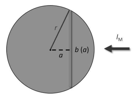
Figure 1.
View on the circular base plane of a cylindrically shaped grain for the determination of the length b(a). The measurement current IM passes through the cylindrical surface.
The relevant areas that must be integrated, consist of rectangles with an area of h·b(a).Using simple geometrical relations and under the consideration of symmetry, the electrical resistance of a single grain can be calculated by:
Thus, the radius of the grain does not influence its total resistance. This is caused by the fact that while on the one hand, the length b(a) increases with increasing r, on the other hand, the integration pathway becomes longer. Both effects compensate for each other, which causes an independence of the resistance from r. Using Equation (4), the total resistance of the L/(2·r) grains in one row is given by:
Finally, the electrical resistance of N rows of grains connected in parallel is calculated by:
As a result, the measured electrical resistance is expected to be inversely proportional to the maximal area r·h of the grain.
3.3. Electrical Resistance of Spherical Grains
Similar to the considerations in Figure 1, the integration area that is required for spherical grains can be determined. In contrast to Equation (4), these areas A(a) are circular:
For rmax = r, the integral diverges—the resistance of a one-point contact is infinite. Thus, a flattening of the contact area has to be assumed. By using rmax = q·r, the integral provides values that depend on the fraction q of the radius which is not affected by the flattening (Table 1). The flattening is only assumed to be present in the direction in which IM is flowing. Note that the area hyperbolic tangent is zero for a = 0.

Table 1.
Solution of the integral in Equation (7) for different values of q.
Depending on assumptions or microstructural images, q can be selected appropriately. The resistance of a row of grains can be determined by:
which leads to:
3.4. Microstructural Investigations of Rolled Sheets
The model described above is particularly suitable for rolling processes because the number of grains in the cross-sections of sheets that were rolled along different processing routes can be assumed to be constant (i.e., N = const.). Thus, the reduction of the cross-sectional area of the sheets due to rolling is implicitly included in the model.
Rolled sheets of the material DC04 were selected in order to provide homogenous microstructural properties across the entire cross-section. In addition, besides the average grain sizes, these properties should not vary strongly for the different sheet thicknesses. Both have been proven by the authors in a previous study [20]. The microstructural properties of crystallite size, microstrain (as a measure for the dislocation density), and texture of different DC04 sheets dependent on their von-Mises equivalent plastic strain φ are shown in Figure 2.
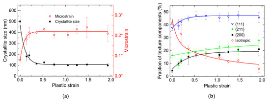
Figure 2.
Crystallite sizes and microstrains (a) as well as fraction of different texture components (b) for different DC04 sheets with different von-Mises equivalent plastic strains. The solid lines are exponential fitting functions.
The microstrain is of particular interest as it does influence the electrical resistivity of the material as lattice defects cause the scattering of electrons. In Figure 2, two additional measurements from a previous study are included for low plastic strains (0.200, 0.140) in order to outline the trend more precisely. Already the first rolling passes causes a rise of the microstrain. This value is almost constant for all further rolling passes. In absolute values, the microstrain does not rise strongly due to the first rolling processes. Thus, the electrical resistivity is expected not to be significantly different for all investigated sheets.
The grains present in the sheets can be approximated by a cylindrical shape (Figure 3).
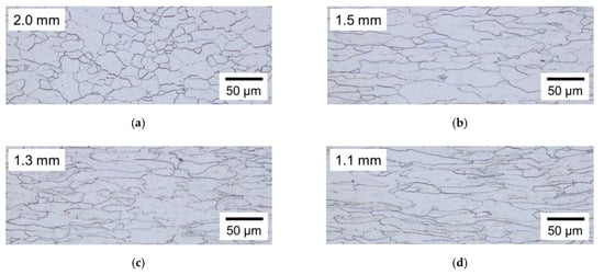
Figure 3.
Optical microscope images of longitudinal sections of DC04 sheets with sheet thicknesses of (a) 2.0 mm, (b) 1.5 mm, (c) 1.3 mm, as well as (d) 1.1 mm.
In Figure 4, the grain sizes across the cross-section of the sheet with ds = 1.3 mm are shown.
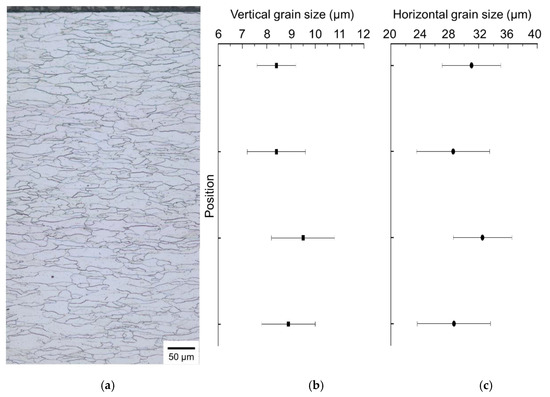
Figure 4.
(a) Optical microscope images of a cross-section of a DC04 sheet with ds = 1.3 mm as well as corresponding (b) vertical and (c) horizontal grain sizes across the sheet thickness. Due to symmetry, only one half of the cross-section of the sheet is shown.
For ds = 1.3 mm, the average grain size in the depth direction (vertical) is (8.7 ± 0.8) µm and in the rolling direction (horizontal) (30 ± 4) µm. Only minor variations occur in either direction. Similarly, no significant variations in the grain size across the sheet thickness could be observed for any of the sheets. Thus, a constant average grain size can be assumed across the entire sheet thickness.
The average grain sizes that were determined using the linear-intercept method as well as the measured electrical resistance are summarized in Table 2.
Table 2.
Average grain sizes (radius and height) and measured electrical resistance in () and perpendicular to () the rolling direction of different sheets. The sheets marked as test sheets serve the purpose of validation.
For the samples with the same final thickness that have been rolled along different processing routes, no significant differences of the average grain size or the electrical resistance were observed. Thus, the mean values include different processing routes for thicknesses of 1.1 mm and 0.9 mm. As expected, the grain elongation h increases with additional rolling passes (i.e., lower sheet thickness), whereas the grain radius r decreases. These changes cause the electrical resistance to rise with decreasing sheet thickness. This will be discussed in the next chapter.
4. Discussion
The different DC04 sheets used vary in their grain sizes, but not in their general grain shape and possess almost identical microstructural properties (with a slight exception for the initial-state 2.0 mm sheet). By using this system, the equations that were derived for cylindrical grains can be tested. Along the rolling direction, Equation (3) can be used. Perpendicular to the rolling direction, Equation (6) is expected be valid. In the following, the validity is proven and a method is shown as to how it can be used to determine grain sizes after a calibration.
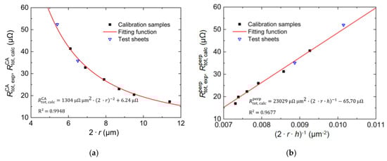
Figure 5.
Electrical resistance of DC04 sheets (a) along the rolling direction in dependence of the grain diameter and (b) perpendicular to the rolling direction in dependence of the reciprocal grain area.
As expected, based on the theoretical considerations, there is a 1/r2 decrease of the electric resistance along the rolling direction (Figure 5a). This decrease can be described well with Equation (3). The fit (R² = 0.9948) that is shown in Figure 5 was achieved using only the “calibration samples”. Nevertheless, the agreement between the fit and the test sheets is very good as well. Even the sheet with ds = 0.5 mm, which has a grain diameter that is smaller than the grain diameters that were used for calibration, shows a low deviation. In the direction perpendicular to the rolling direction of the sheets (Figure 5b), the inverse linear relation of the electrical resistance regarding the grain area (2·r·h) that is predicted by Equation (6) is confirmed with a very good agreement (R² = 0.9677) of the experimental data and the fit. The test sheets only slightly deviate from the fit. The values of N are 190,430 in the rolling direction and 13,288 perpendicular to the rolling direction. Due to their smaller cross-sectional area, the number of grains in the rolling direction with a relevant contribution to the measured resistance is larger than those perpendicular to the rolling direction. Even though the relevant area could be calculated from N, no statements can be made concerning its shape or the maximum information depth of the measurement in the course of the model.
These results prove the validity of the Equations (3) and (6). However, the grain sizes cannot be determined without a calibration as both equations contain two or three parameters (N, r, and h) that cause the measured resistance value. The determination of grain sizes of different samples that were produced by rolling is possible using the following approach under the assumption of (aligned) cylindrically shaped grains:
- Determination of the relevant grain sizes (r and h) of at least four to five calibration samples;
- Measurement of the electrical resistance along and perpendicular to the grain (cylinder) axis for these calibration samples;
- Fitting of the Equations (3) and (6) as shown in Figure 5a,b respectively. The fits do determine and fix N for the subsequent steps;
- Measurement of the electrical resistance along and perpendicular to the grain axis for samples with unknown grain sizes;
- By using the fitting function (along the grain axis), r can be determined;
- By using the fitting function (perpendicular to the grain axis) and r (step 5.), h can be calculated.
This approach as well as the underlying model were shown to be valid for constant grain sizes across the individual samples that had been produced by rolling processes. However, the model faces some limitations due to the assumptions that were made:
- Grain-size distributions cannot be determined. If a wide grain-size distribution is present, an average will be calculated that inaccurately describes the microstructure. In particular, bimodal grain-size distributions with very small and very large grains will cause the results to be inaccurate;
- The grain shape and orientation must be known;
- The grains in the sample can only be approximated by the idealized grain shape of a cylinder or sphere. Thus, the size of an equivalent cylinder or sphere will be determined when using the model;
- Depth gradients of the grain sizes or shapes cannot be analyzed. When measuring non-homogeneous samples, an average grain size will be determined, but due to the proportionality of the resistance to r−2, smaller grains will be stronger weighted;
- If the microstrain, i.e., the dislocation density, differs significantly across the sample, local differences in the specific resistance of the grains occur. Thus, the average specific resistance would differ from the assumed value in Equations (3), (6) and (9), which causes the calculated grain sizes to be shifted systematically. However, this effect is considered to be smaller than differences in the grain size because the equations only depend on the specific resistance linearly, and the relative change in the specific resistance of the grains is expected to be small.
5. Conclusions
An analytical model was developed that allows for the determination of grain sizes by the measurement of the electrical resistance by means of the four-point probe method. This model is specifically designed for bulk material with a constant grain size across the entire cross-section. The most common grain shapes, cylinder and sphere, were considered. Based on Equations (3), (6) and (9), a calibration with known grain sizes can be performed. Using this calibration, unknown grain sizes can be determined.
Due to the limitation that were mentioned in Section 4, the method is particularly appropriate for cold-rolling processes. In such processes, the assumption of constant grain sizes and grain shapes within each individual sample, as well as unaltered crystallite sizes and dislocation densities across the consecutively rolled samples, is true. In the cold-rolling process of DC04, different processing routes for achieving the same final thickness lead to the same microstructure and thus the same measured electrical resistance values.
The model can easily be extended to homogeneously distributed bimodal grain-size distributions if the number fractions of both grain sizes are known. Layer stacks, e.g., a surface layer with bulk material underneath, could be described by an extended model if additional assumptions concerning the resistance-impacting area are made.
Author Contributions
Conceptualization, T.M. and T.L.; methodology, T.M.; validation, T.M.; investigation, M.U.; writing—original draft preparation, T.M.; writing—review and editing, T.L. and M.U.; supervision, T.L. All authors have read and agreed to the published version of the manuscript.
Funding
The scientific work has been supported by the German Research Foundation (DFG) within the research priority program SPP 2086 (SCHU1484/26-1, LA 1274/49-1) grant number 401805994. The authors thank the DFG for this funding and intensive technical support.
Institutional Review Board Statement
Not applicable.
Informed Consent Statement
Not applicable.
Data Availability Statement
Data available on request due to restrictions eg privacy or ethical. The data presented in this study are available on request from the corresponding author. The data are not publicly available due to ongoing research activities.
Acknowledgments
The authors thank the Virtual Production Engineering group at the Chemnitz University of Technology for the provision of the materials used for the experiments.
Conflicts of Interest
The authors declare no conflict of interest.
References
- Turnbull, A.; De Los Rios, E.R. The Effect of Grain Size on the Fatigue of commercially pure Aluminium. Fatigue Fract. Eng. Mater. Struct. 1995, 18, 1455–1467. [Google Scholar] [CrossRef]
- Ralston, K.D.; Birbilis, N.; Davies, C.H.J. Revealing the relationship between grain size and corrosion rate of metals. Scr. Mater. 2010, 63, 1201–1204. [Google Scholar] [CrossRef]
- Mayadas, A.F.; Shatzkes, M. Electrical-Resistivity Model for Polycrystalline Films: The Case of Arbitrary Reflection at External Surfaces. Phys. Rev. B 1970, 1, 1382–1389. [Google Scholar] [CrossRef]
- Tellier, C.R. Size and Grain-Boundary Effects in the Electrical Conductivity of Thin Monocrystalline Films. Electrocompon. Sci. Technol. 1978, 5, 127–131. [Google Scholar] [CrossRef]
- Bedda, M.; Messaadi, S.; Pichard, C.R.; Tosser, A.J. Analytical expression for the total electrical conductivity of unannealed and annealed metal films. J. Mater. Sci. 1986, 21, 2643–2647. [Google Scholar] [CrossRef]
- Luo, W.; Zhu, L.-L.; Zheng, X.-J. Grain Size Effect on Electrical Conductivity and Giant Magnetoresistance of Bulk Magnetic Polycrystals. Chin. Phys. Lett. 2009, 26, 117502. [Google Scholar] [CrossRef]
- Durkan, C.; Welland, M.E. Size effects in the electrical resistivity of polycrystalline nanowires. Phys. Rev. B 2000, 61, 14215–14218. [Google Scholar] [CrossRef]
- Mannan, K.M.; Karim, K.R. Grain boundary contribution to the electrical conductivity of polycrystalline Cu films. J. Phys. F Met. Phys. 1975, 5, 1687–1693. [Google Scholar] [CrossRef]
- Lim, J.W.; Isshiki, M. Electrical resistivity of Cu films deposited by ion beam deposition: Effects of grain size, impurities, and morphological defect. J. Appl. Phys. 2006, 99, 094909. [Google Scholar] [CrossRef]
- Plombon, J.J.; Andideh, E.; Dubin, V.M.; Maiz, J. Influence of phonon, geometry, impurity, and grain size on Copper line resistivity. Appl. Phys. Lett. 2006, 89, 113124. [Google Scholar] [CrossRef]
- Kumar, A.; Singh, D.; Kaur, D. Grain size effect on structural, electrical and mechanical properties of NiTi thin films deposited by magnetron co-sputtering. Surf. Coat. Technol. 2009, 203, 1596–1603. [Google Scholar] [CrossRef]
- Day, M.E.; Delfino, M.; Fair, J.A.; Tsai, W. Correlation of electrical resistivity and grain size in sputtered titanium films. Thin Solid Film. 1995, 254, 285–290. [Google Scholar] [CrossRef]
- Moriyama, M.; Kawazoe, T.; Tanaka, M.; Murakamia, M. Correlation between microstructure and barrier properties of TiN thin films used Cu interconnects. Thin Solid Film. 2002, 416, 136–144. [Google Scholar] [CrossRef]
- Learn, A.J.; Foster, D.W. Resistivity, grain size, and impurity effects in chemically vapor-deposited tungsten films. J. Appl. Phys. 1985, 58, 2001–2007. [Google Scholar] [CrossRef]
- Zeng, H.; Wu, Y.; Zhang, J.; Kuang, C.; Yue, M.; Zhou, S. Grain size-dependent electrical resistivity of bulk nanocrystalline Gd metals. Prog. Nat. Sci. Mater. Int. 2013, 1, 18–22. [Google Scholar] [CrossRef]
- Santos, T.G.; Miranda, R.M.; Vilaça, P.; Teixeira, J.P. Modification of electrical conductivity by friction stir processing of aluminum alloys. Int. J. Adv. Manuf. Technol. 2011, 57, 511–519. [Google Scholar] [CrossRef]
- Metan, V.; Eigenfeld, K. Controlling mechanical and physical properties of Al-Si alloys by controlling grain size through grain refinement and electromagnetic stirring. Eur. Phys. J. Spéc. Top. 2013, 220, 139–150. [Google Scholar] [CrossRef]
- Barghout, J.Y.; Lorimer, G.W.; Pilkington, R.; Prangnell, P.B. The Effects of Second Phase Particles, Dislocation Density and Grain Boundaries on the Electrical Conductivity of Aluminium Alloys. Mater. Sci. Forum 1996, 217–222, 975–980. [Google Scholar] [CrossRef]
- Abbas, S.F.; Seo, S.-J.; Park, K.-T.; Kim, B.S.; Kim, T.-S. Effect of grain size on the electrical conductivity of copper–iron alloys. J. Alloys Compd. 2017, 720, 8–16. [Google Scholar] [CrossRef]
- Mehner, T.; Bauer, A.; Awiszus, B.; Lampke, T. Macromechanical finite-element simulations for predicting microstructures by experimental calibration. IOP Conf. Ser. Mater. Sci. Eng. 2017, 181, 12036. [Google Scholar] [CrossRef]
Publisher’s Note: MDPI stays neutral with regard to jurisdictional claims in published maps and institutional affiliations. |
© 2020 by the authors. Licensee MDPI, Basel, Switzerland. This article is an open access article distributed under the terms and conditions of the Creative Commons Attribution (CC BY) license (http://creativecommons.org/licenses/by/4.0/).