1. Introduction
With the increasing power dissipation and shrinking feature sizes of high-power devices (such as insulated gate bipolar translator, central processing unit, laser load devices, etc.), the heat generated is gradually increasing. High temperature has a bad impact on the performance of power devices. Research shows that the device failure rate doubles and the lifespan of the devices is halved for every 10 °C rise in the joining temperature [
1], and that more than 55% of the failures of electronic devices are caused by too-high temperatures [
2]. Therefore, high requirements for heat dissipation are established [
3], and some efficient heat sinks (such as heat pipe, microchannel, refrigeration chip, etc.) have been developed. As such, the interfacial heat transfer between heat source and heat sink is becoming a severe bottleneck, currently limiting the further scaling of performance. Meanwhile, the heat flux density through the interface is constantly increasing [
4], so interfacial heat transfer enhancement is essential for the development of high-power devices. The common methods used currently are as follows: adding thermally conductive particles (i.e., metals, ceramics) to nonmetallic thermal interface materials (TIM) [
5] and using low melting temperature alloy (LMTA) [
5], etc. However, the thermal conductivity of nonmetallic materials is lower than that of metallic materials, and thermal greases are easy to age. The LMTA and some nonmetallic TIM are in the liquid state in the service process, and are easy to flow out, which affects the reliability negatively [
6], and external pressure is needed for them [
5,
6]. Thus, the metallurgical bonding of mating surfaces is the best choice for interfacial heat transfer enhancement.
Considering the special working conditions of some power devices, they must be assembled at low temperatures. For example, the aluminum ammonia heat pipe must be assembled under 95 °C, and the laser generator cannot exceed 80 °C. At the same time, they often work at a temperature that is close to or even higher than the bonding temperature. Therefore, the reliability of the bonded surfaces will not decrease at higher temperatures. At present, the methods that can be used for low-temperature bonding with high reliability include nanoparticle sintering technology, transient liquid phase sintering (TLP) and solid-liquid inter-diffusion bonding (SLID), etc.
Nanoparticle sintering technology can meet the above requirements, and the electrical and thermal conductivity [
7,
8] and mechanical properties [
9,
10,
11] of the joints are excellent. However, its bonding temperature is generally higher than 200 °C [
12], which is still too high for many power chips or devices. The interfacial microstructure has significant porosity, which will reduce the thermal and mechanical properties of the joints [
13]. Besides, this technology costs a lot, given the high price of Ag. Its microstructure and properties cannot be improved under the action of high service temperature, and they will deteriorate at high temperatures and with long-term service.
Therefore, metallurgical bonding with a uniform interfacial microstructure is an important solution to this problem. The TLP sintering used mostly in the microelectronic packaging industry, also known as SLID [
14], is a good way to solve this problem. It uses a high melting point metal and a low melting point metal to form intermetallic compounds (IMC), which melt at higher temperatures than the bonding temperature during isothermal solidification [
15].
In this paper, the low temperature metallurgical bonding of copper substrates is investigated. The Cu substrates were successfully bonded with a self-made interlayer at 100 °C without any flux. Then, the microstructure, shear strength, temperature resistance and thermal contact conductance of the joints were studied, and the mechanism of Cu/Ga SLID bonding was discussed.
2. Materials and Methods
In this paper, we chose Ga as the low melting point metal, for the melting point of Ga (29.75 °C) is lower than Sn (231.9 °C) and In (156.6 °C), and the processing temperature of Ga-based solder is lower. Besides, gallium has excellent wetting properties and can decrease melting temperature, and so on. [
16,
17]. Although the eutectic points of Ga-Sn and Ga-In are lower than the melting point of Ga, the bonding temperature of Ga-based solder can completely meet our requirements. Besides, more work needs to be done on the interaction between Ga-based solder and components at low temperatures to fully utilize this kind of interesting material, and expedite its use in industry [
17].
Cu substrates are utilized via their widespread use as metallization materials [
18]. We chose Cu as the high melting point metal. The Au/Ga system has been investigated [
19], as has the very high diffusion speed of gold into liquid Ga during the process expediting the extreme formation of kirkendall voids. The solderability of the Ag/Ga system is poor. The inter-diffusion coefficient of Cu/Ga is appropriate [
20], but the Cu/Ga system has been rarely used, and they often introduce Au or Pt as a seed layer [
21,
22].
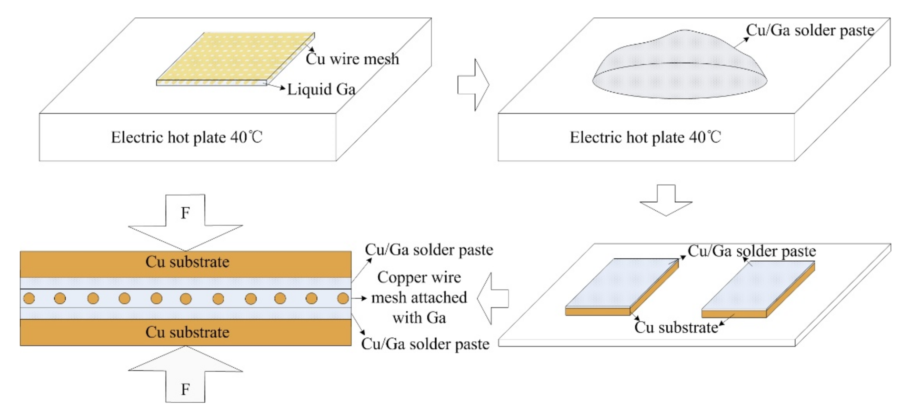
Cu/Ga solder paste and copper wire mesh attached with liquid Ga were used to prepare the self-made interlayer. Copper wire mesh plays the role of skeleton, which can help keep the thickness of the interlayer uniform. The Cu content in the interlayer was optimized to be about 33 wt. %, corresponding to the stoichiometry of the main reaction of copper with gallium at a small copper excess. In the whole bonding process, gallium is in the liquid state, and solid copper is surrounded by a liquid, which greatly shortens the atom diffusion distance and makes Cu/Ga inter-diffusion easy. The requirement of the substrate roughness and flatness is not high.
The copper wire mesh is pure copper, with a purity of 99.9%, 400 mesh and diameter of 40 μm. The particle size of the copper powder is 300 mesh. The purity of gallium is 99.9%. The size of the copper substrate is 60 mm × 10 mm × 1.5 mm. The materials were provided by the China General Research Institute of Nonferrous Metals. The copper substrate and copper wire mesh will be pretreated to remove the oil and oxide film on surface before joining.
Bonding process: (1) Coat the copper wire mesh with liquid Ga uniformly at 40 °C; (2) Prepare the Cu/Ga solder paste at 40 °C. Ga exists in a liquid state at 40 °C and has excellent wettability, so copper powder can be wetted by liquid Ga completely without any flux to obtain silver white Cu/Ga solder paste; (3) Apply Cu/Ga solder paste on the surface of the Cu substrates uniformly; (4) Place the copper wire mesh attached with liquid Ga between the two Cu substrates in fixture with pressure of 2 MPa; (5) Subsequently, the assembled samples are held in the furnace at 100 °C for 10 h, 20 h and 30 h respectively; (6) Take out the samples from the furnace for further observation and testing.
Figure 1 shows the schematic diagram of the bonding process.
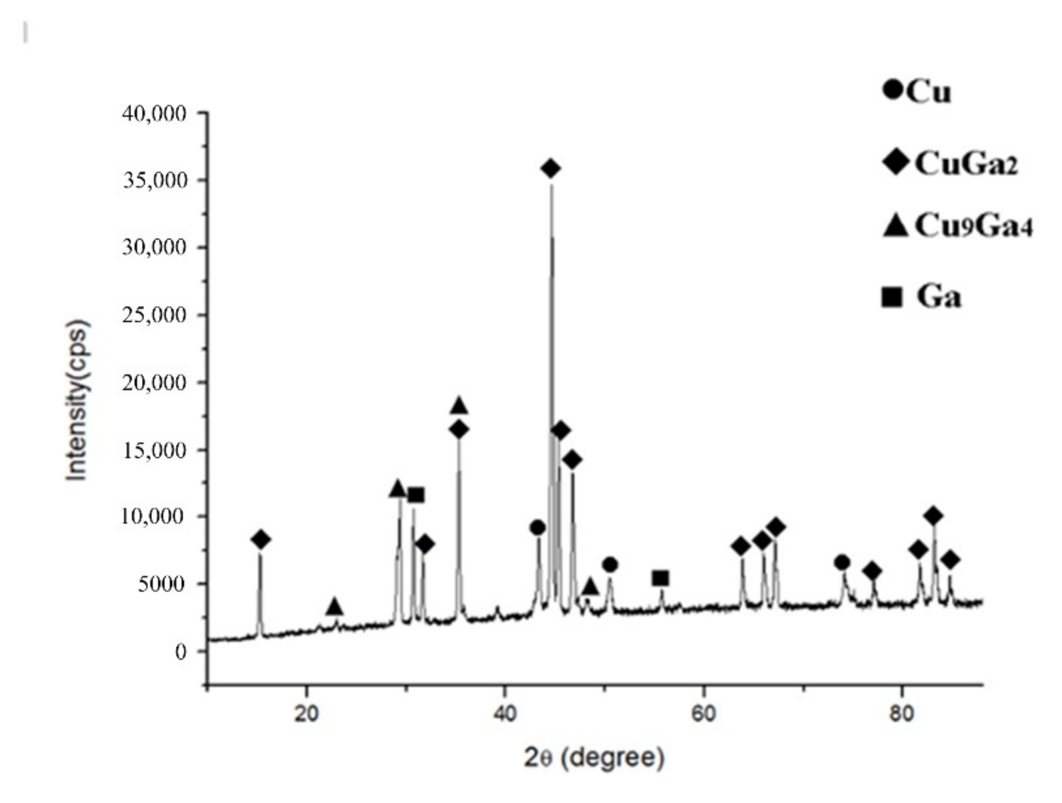
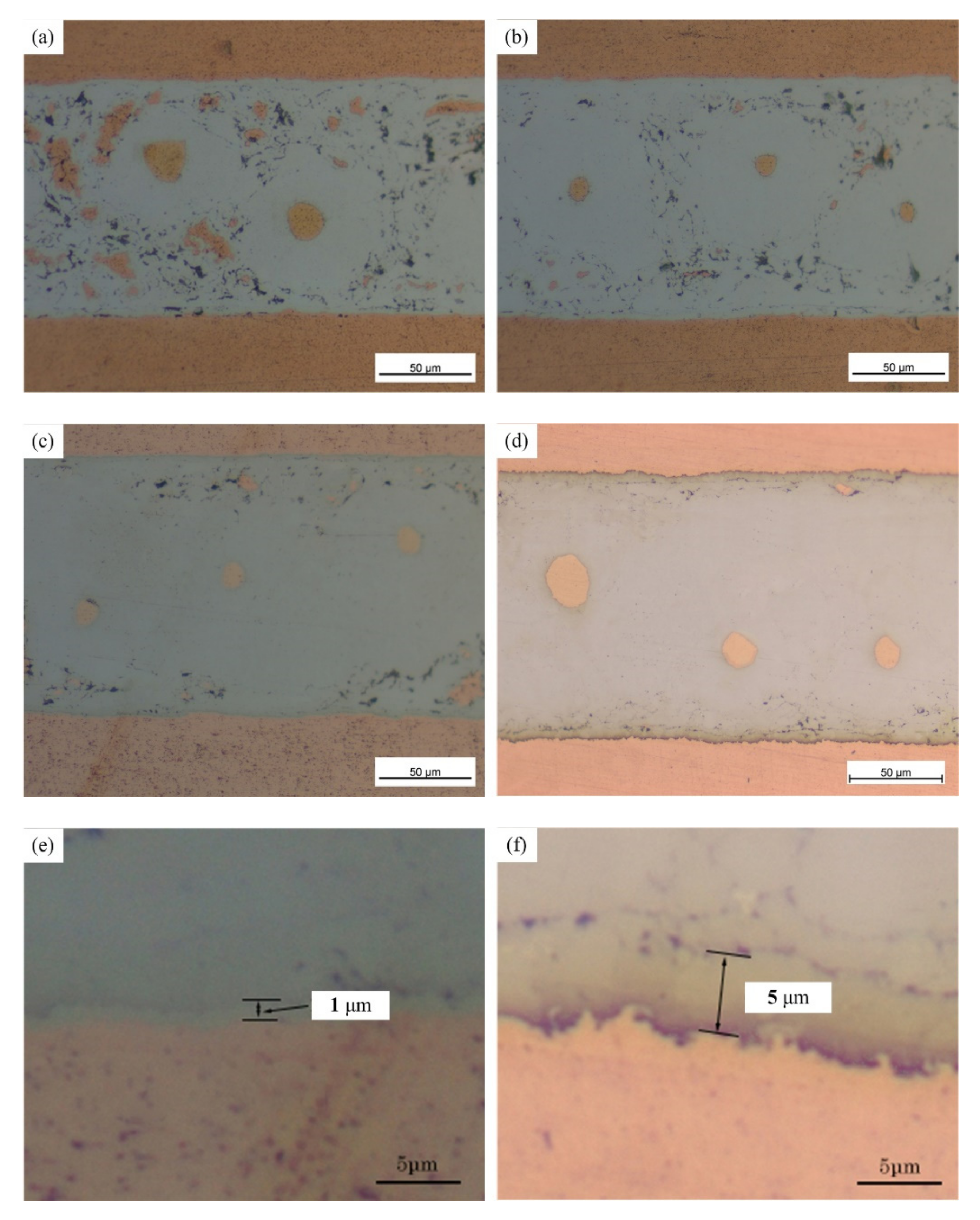
An optical microscope (OM) (Olympus B×5) and a scanning electron microscope (SEM) (JSM-7500) were used to investigate the interfacial microstructure of the joints. The phase constitutions of the intermediate layer were analyzed by X-ray diffraction (XRD) tests with with X-ray diffractometer (D/Max-2200pc). The X-ray source is excited by the copper target. The working voltage and current were 40 kV and 40 mA, respectively, and the scanning speed was set at 6 degrees per minute. Micro-area composition analysis was investigated via Energy dispersive spectrometry (EDS) detected with SEM. The EDS analysis was performed with an acceleration voltage of 20 kV. Firstly, the joints were cut and fixed with bakelite power to make metallographic specimens. The specimens were ground with 260, 800, 1200 and 2000 waterproof abrasive paper, and then polished with 2 μm and 0.5 μm diamond paste. The XRD and SEM tests were conducted first, and etching was performed before the OM tests.
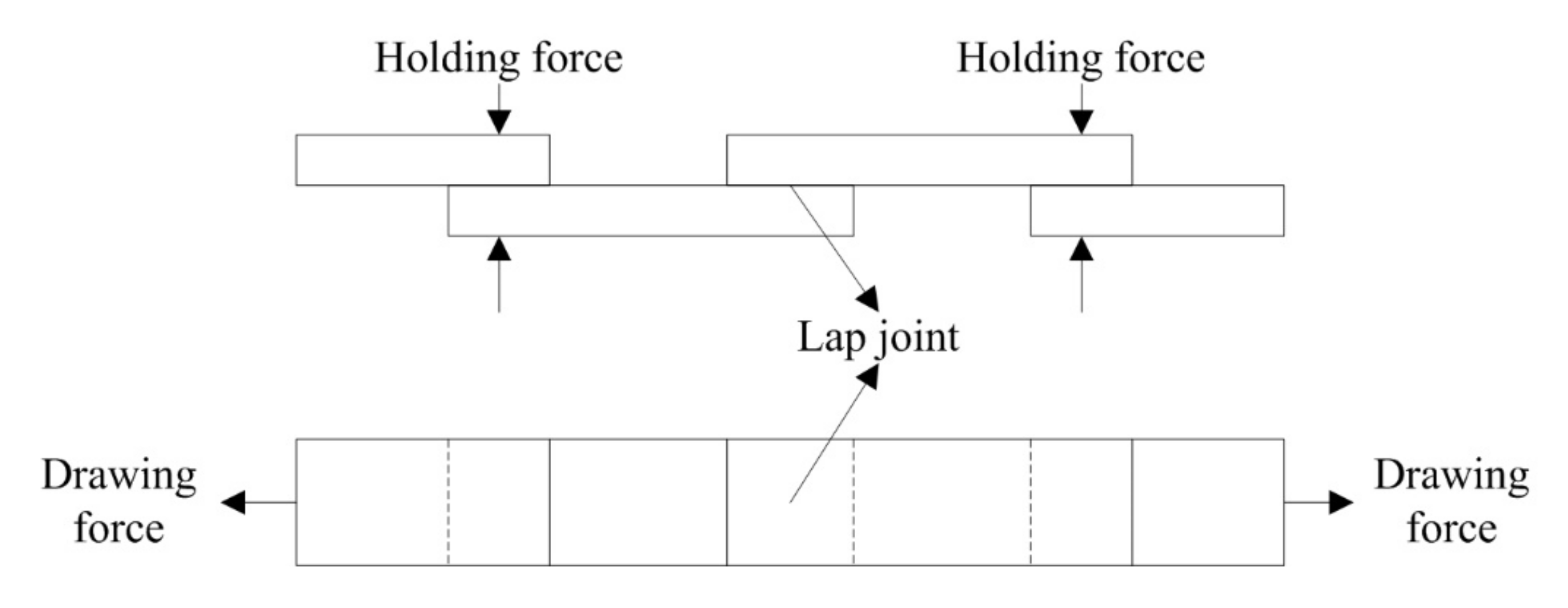
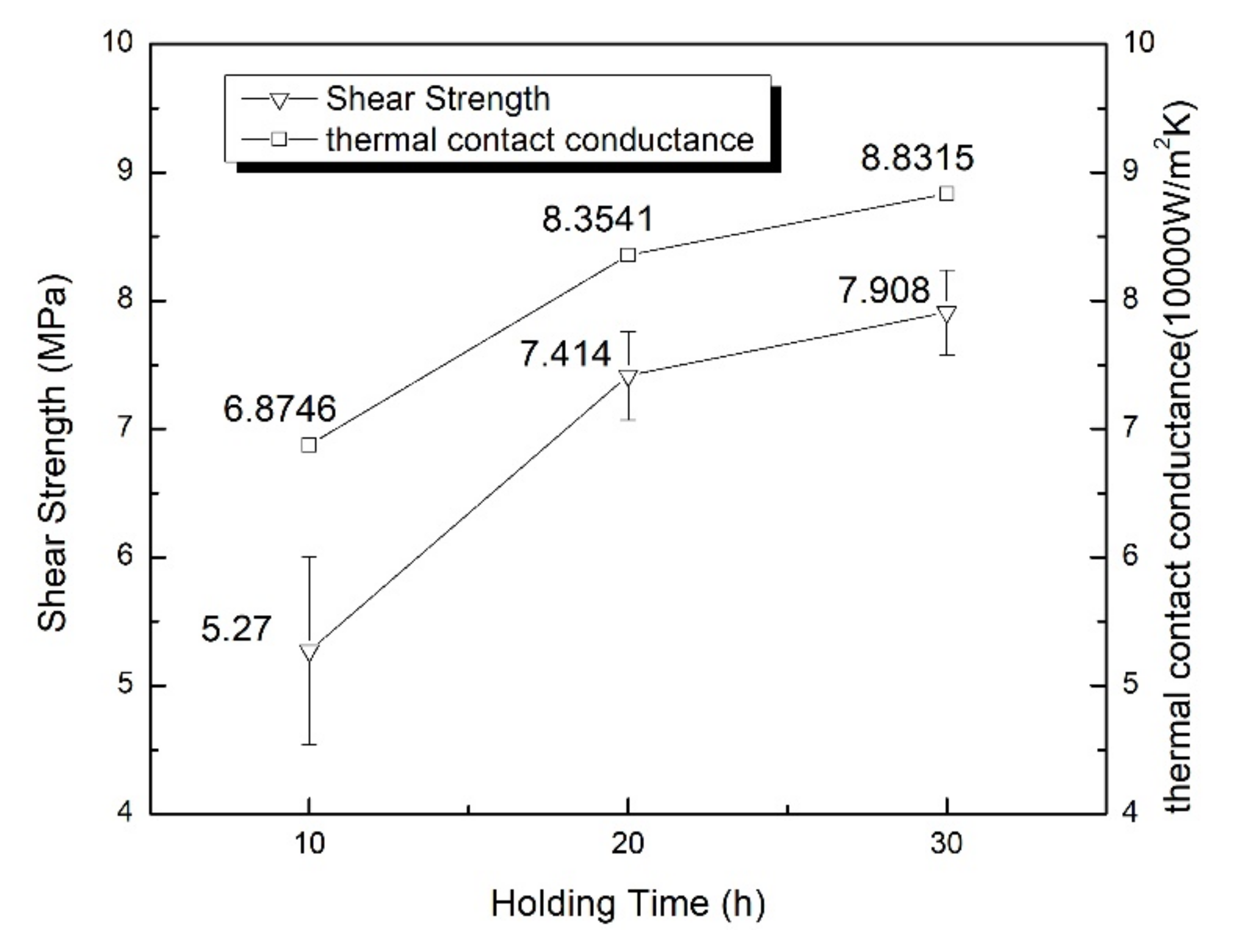
The mechanical properties of the joints were evaluated by shear testing at room temperature using a tensile testing machine (MTS50KN) with a machine displacement rate of 0.5 mm/min. The average shear strength of five joints was used to contrast the mechanical property. The joint used was the lap joint, and the lap length was 5 mm. If the tension center and the sample center are not in a straight line, the test results will be inaccurate. Two small pieces were bonded at both ends of the lap joint, as shown in
Figure 2. When holding the samples on the fixture of the testing machine, attention should be paid to the position of the samples so as to prevent eccentricity.
The method of the temperature resistance test is the weight method. A certain load is applied to the specimen, and then the specimen is heated to a predetermined temperature to observe whether the joint is remelted at this temperature. The test was carried out in a resistance furnace, and holes were punched on each piece of the lap joint respectively to hang the weight of 50 g, as shown in
Figure 3. After several minutes, the specimens reached the preset temperature of 200 °C. The specimens were hold at this temperature for 10 min to observe the joints.
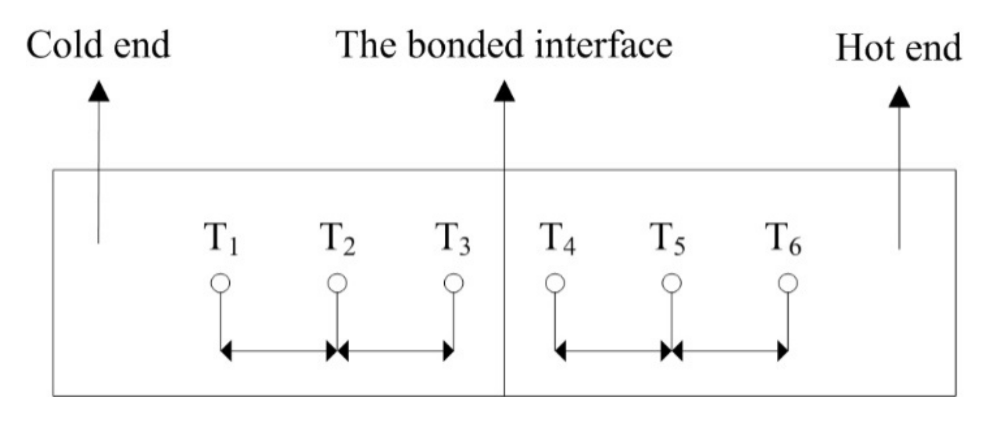
The thermal property is evaluated by the thermal contact conductance of the bonded interface, using infrared-assisted steady state temperature measurement of the vacuum thermocouple. The rated heat flux (q) was selected as 10, 50, 100, 200 and 300 W/cm
2, and the simulation device for the test was designed according to the basic law of heat conduction (Fourier law), as shown in
Figure 4. The material was copper, and the thermal conductivity of Cu is 427 W/(m·K) [
6]. The whole device was wrapped with multi-layer thermal insulation material and put into the vacuum tank on a special test bench for testing. The heat transfer from the hot end to the cold end can be regarded as one-dimensional axial heat conduction. From the three temperature measurement points of the cold end, the temperature value of the cold end at the bonded interface can be obtained by linear fitting. Similarly, the temperature value of the hot end at the bonded interface can be obtained. The difference between the two temperature values is the heat transfer temperature difference of the bonded interface △T. q/△T is the thermal contact conductance of the bonded interface.
4. Discussion
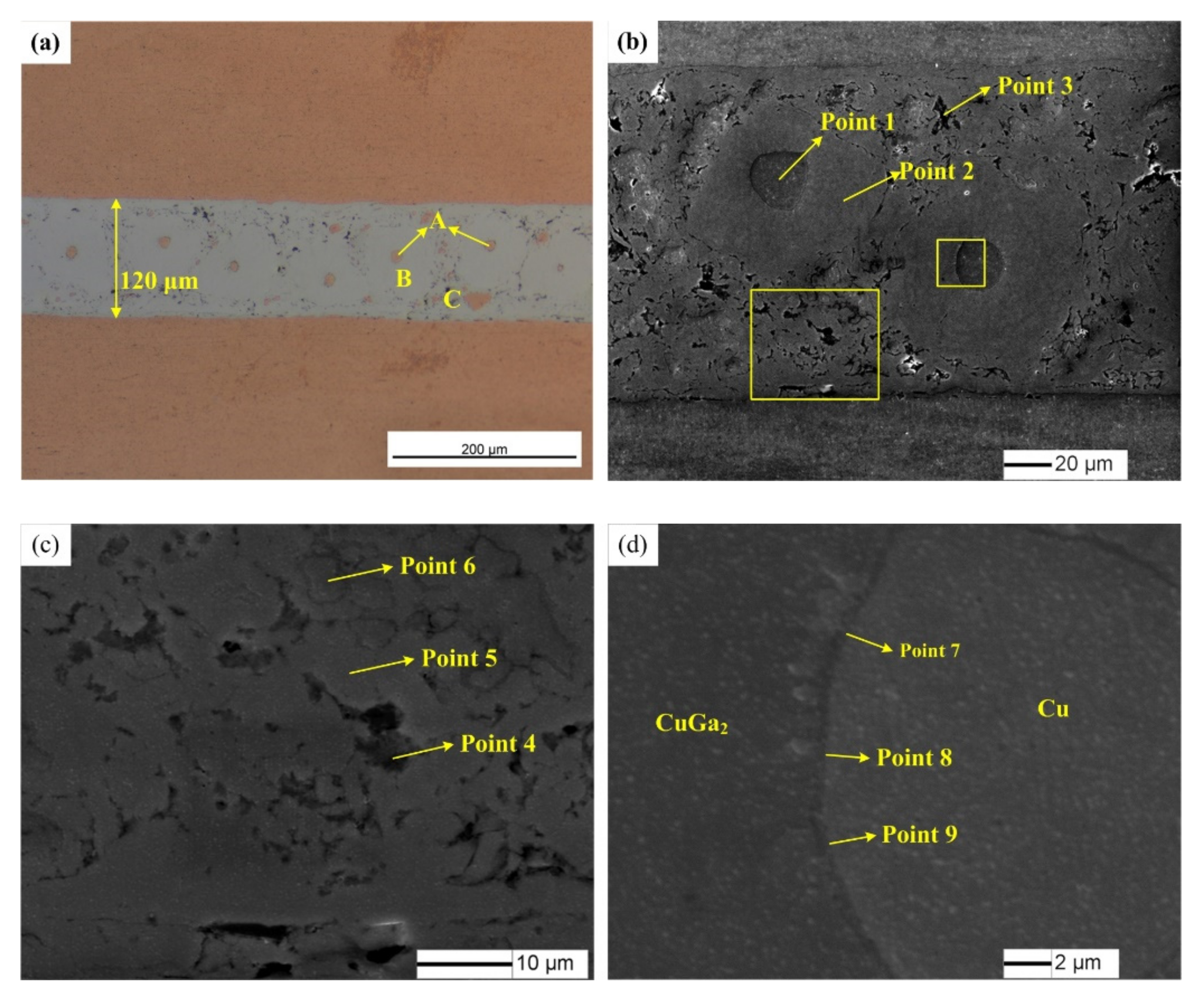
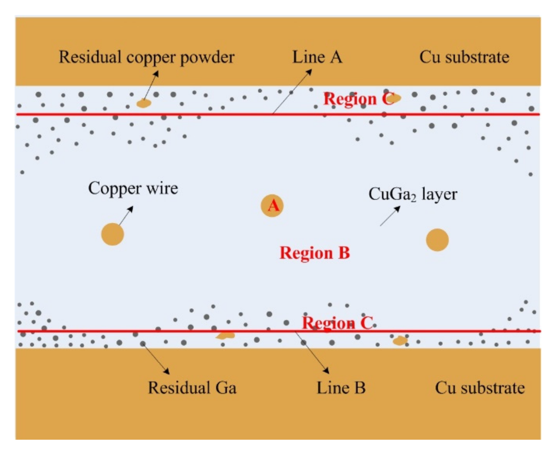
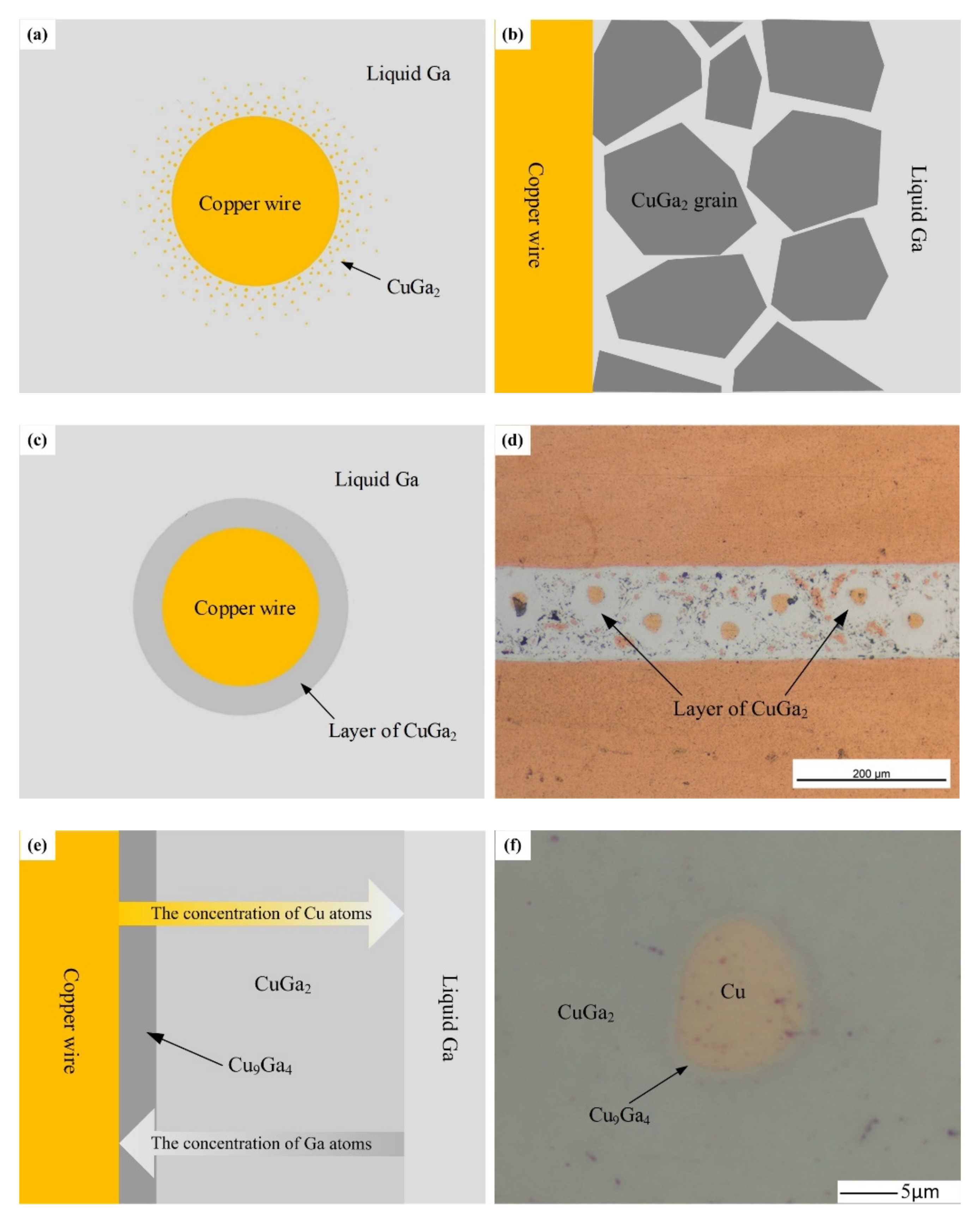
During the heat preservation process, liquid gallium and solid copper wire, and copper powder and copper substrate, interdiffuse and react with each other. The whole process of Cu/Ga SLID bonding is divided into the following three stages:
(1) Pressurization stage—Apply a certain amount of pressure to the joint in the heat preservation process. Liquid Ga is forced to flow into the gap in the copper wire mesh under the pressure to discharge the air mixed in the bonding process, thus the pressure in the interlayer tends to be the same. It can also increase the pressure of the solid/liquid interface, so that the contact between the solid copper and liquid gallium is more sufficient for subsequent diffusion;
(2) Reaction diffusion stage—Driven by a high temperature and concentration gradient, surface diffusion occurred rapidly at the solid Cu/liquid Ga interface to form θ-CuGa
2 phase. The θ-CuGa
2 phase formed due to the fast diffusion kinetics of Cu to liquid gallium [
35]. The copper atoms on the solid copper surface diffuse into the surrounding liquid Ga and react rapidly with it to form θ-CuGa
2, as shown in
Figure 10a. With the increase in the θ-CuGa
2 compound, θ-CuGa
2 crystals begin to precipitate, as shown in
Figure 10b. Then, the θ-CuGa
2 layer gradually forms, as shown in
Figure 10c. Above is the formation process of intermetallic compound θ-CuGa
2. After that, the solid copper and liquid gallium are separated by a θ-CuGa
2 layer, and the reaction diffusion will be hindered, as shown in
Figure 10d. At this time, the θ-CuGa
2 phase may contain a higher amount of Ga [
35].
Froemel thinks [
21] that the increased diffusion of the solid phase into the liquid phase leads to a rapid increase of the Cu atoms inside the liquid Ga. After reaching a saturation of solubility, intermetallic compounds are formed, and thus solidification happens. According to the Cu/Ga binary phase diagram [
23,
24], when the concentration of copper is more than 1%, the liquid’s temperature will exceed 100 °C. This means that there will be a solid phase when the concentration of copper is 1~33.3% at 100 °C if the Cu/Ga solution is formed first, which is contrary to the fact. Therefore, in the early stage of the diffusion, the copper atoms react immediately with Ga to form θ-CuGa
2 phase, and do not form the Cu/Ga solution;
(3) Isothermal solidification stage—This stage takes a long time. The main mode of the atoms passing through the θ-CuGa2 layer is grain boundary diffusion and vacancy diffusion. In the early stage of the θ-CuGa2 layer formation, the grains grow up gradually, the grain boundary gap is large, most of the grain boundaries are large angle grain boundaries, and the grain boundary energy is high. When the concentration gradient is certain, the activation energy required for copper atoms to cross the grain boundaries is low, which makes it easy to diffuse through the grain boundaries. At the same time, gallium atoms also move across the grain boundaries to the solid copper. At high temperatures, there is a certain concentration of vacancy in the θ-CuGa2 crystal. Driven by the concentration gradient, copper atoms can also migrate to liquid gallium through vacancy diffusion. In later stages of grain boundary diffusion, vacancy diffusion will play a more important role.
Copper atoms migrate from the solid copper surface, across the θ-CuGa
2 layer, to liquid gallium by grain boundary diffusion and vacancy diffusion. As shown in
Figure 10e, from left to right on the θ-CuGa
2 layer, the concentration of copper atoms decreases gradually, and the concentration of gallium atoms increases gradually. Because the copper atom content in the θ-CuGa
2 layer on the side of the copper wire is relatively high, a new intermetallic compound, γ
3-Cu
9Ga
4 (2θ-CuGa
2+7Cu = γ
3-Cu
9Ga
4), is gradually generated. The γ
3-Cu
9Ga
4 generated is located at the interface of the copper wire and θ-CuGa
2 layer. Then, a thin γ
3-Cu
9Ga
4 layer is gradually formed as time goes on, as shown in
Figure 10f. As the gallium atom content in the θ-CuGa
2 layer on the side of liquid gallium is high, Ga reacts with the diffused copper atom to form θ-CuGa
2. On the micro level, θ-CuGa
2 grains grow and the θ-CuGa
2 grain boundaries become more flat and narrower. On the macro level, the solid–liquid interface advances in the direction of liquid gallium. Ideally, all liquid Ga in the interlayer will be completely transformed into the solid phase if the holding time is long enough.
Author Contributions
Conceptualization, W.Q. and H.Z. (Hongshou Zhuang); methodology, W.Q. and G.M.; validation, W.Q. and Y.Z.; formal analysis, W.Q. and G.M.; investigation, G.M. and H.Z. (Haiyun Zhu); resources, G.M. and H.Z. (Haiyun Zhu); data curation, G.M.; writing—original draft preparation, G.M.; writing—review and editing, W.Q. and Y.Z.; supervision, W.Q. and Y.Z.; project administration, W.Q.; funding acquisition, W.Q. All authors have read and agreed to the published version of the manuscript.
Funding
This project was funded by key special projects of the national key R&D program (2017YFB0305700).
Acknowledgments
All the authors of this paper sincerely thank the teachers of the testing center of the school of materials science and engineering in Beihang university, and the China academy of space technology for their help in performance testing. This work was supported by key special projects of the national key R&D program (2017YFB0305700).
Conflicts of Interest
The authors declare no conflict of interest.
References
- Belhardja, S.; Mimounia, S.; Saidanea, A.; Benzohra, M. Using microchannels to cool microprocessors: A transmission-line-matrix study. Microelectron. J. 2003, 34, 247–253. [Google Scholar] [CrossRef]
- Yeh, L.T. Review of heat transfer technologies in electronic equipment. J. Electron. Packag. Trans. ASME 1995, 117, 333–339. [Google Scholar] [CrossRef]
- Moore, A.L.; Shi, L. Emerging challenges and materials for thermal management of electronics. Mater. Today 2014, 17, 163–174. [Google Scholar] [CrossRef]
- Ebadian, M.A.; Lin, C.X. A review of high-heat-flux heat removal technologies. J. Heat Transf. 2011, 133, 110801. [Google Scholar] [CrossRef]
- Gwinn, J.P.; Webb, R.L. Performance and testing of thermal interface materials. Microelectron. J. 2003, 34, 215–222. [Google Scholar] [CrossRef]
- Hansson, J.; Torbjörn, M.J.N.; Ye, L.L.; Liu, J. Novel nanostructured thermal interface materials: A review. Int. Mater. Rev. 2017, 63, 22–45. [Google Scholar] [CrossRef]
- Mei, Y.H.; Wang, T.; Cao, X.; Chen, G.; Lu, G.Q.; Chen, X. Transient Thermal Impedance Measurements on Low-Temperature-Sintered Nanoscale Silver Joints. J. Electron. Mater. 2012, 41, 3152–3160. [Google Scholar] [CrossRef]
- Bai, J.G.; Zhang, Z.Z.; Calata, J.N.; Lu, G. Low-Temperature Sintered Nanoscale Silver as a Novel Semiconductor Device-Metallized Substrate Interconnect Material. IEEE Trans. Compon. Packag. Technol. 2006, 29, 589–593. [Google Scholar] [CrossRef]
- Fu, S.C.; Mei, Y.H.; Lu, G.Q.; Li, X.; Chen, G.; Chen, X. Pressureless sintering of nanosilver paste at low temperature to join large area (≥100 mm2) power chips for electronic packaging. Mater. Lett. 2014, 128, 42–45. [Google Scholar] [CrossRef]
- Chen, G.; Yu, L.; Mei, Y.H.; Li, X.; Chen, X.; Lu, G.Q. Uniaxial ratcheting behavior of sintered nanosilver joint for electronic packaging. Mater. Sci. Eng. A 2014, 591, 121–129. [Google Scholar] [CrossRef]
- Yan, J.F.; Zou, G.S.; Wu, A.P.; Ren, J.L.; Yan, J.C.; Hu, A.M.; Zhou, Y. Pressureless bonding process using Ag nanoparticle paste for flexible electronics packaging. Scr. Mater. 2012, 66, 582–585. [Google Scholar] [CrossRef]
- Wang, S.A.; Li, M.Y.; Ji, H.J.; Wang, C.Q. Rapid pressureless low-temperature sintering of Ag nanoparticles for high-power density electronic packaging. Scr. Mater. 2013, 69, 789–792. [Google Scholar] [CrossRef]
- Youssef, T.; Rmili, W.; Woirgard, E.; Azzopardi, S.; Vivet, N.; Martineau, D.; Meuret, R.; Quilliec, G.L.; Richard, C. Power modules die attach: A comprehensive evolution of the nanosilver sintering physical properties versus its porosity. Microelectron. Reliab. 2015, 55, 1997–2002. [Google Scholar] [CrossRef]
- Sun, L.; Chen, M.H.; Zhang, L.; He, P.; Xie, L.S. Recent progress in SLID bonding in novel 3D-IC technologies. J. Alloys Compd. 2020, 818, 152825. [Google Scholar] [CrossRef]
- Jung, D.H.; Sharma, A.; Mayer, M.; Jung, J.P. A review on recent advances in transient liquid phase (TLP) bonding for thermoelectric power module. Rev. Adv. Mater. Sci. 2018, 53, 147–160. [Google Scholar] [CrossRef]
- Matsushita, M.; Sasaki, Y.; Ikuta, Y. Investigation of a New Sn–Cu–Ga Alloy Solder. Defect Diffus. Forum 2011, 312, 518–523. [Google Scholar] [CrossRef]
- Liu, S.; Sweatman, K.; McDonald, S.; Nogita, K. Ga-Based Alloys in Microelectronic Interconnects: A Review. Materials 2018, 11, 1384. [Google Scholar] [CrossRef]
- Ramm, P.; Lu, J.J.Q.; Taklo, M.M.V. Thermocompression Cu–Cu Bonding of Blanket and Patterned Wafers. In Handbook of Wafer Bonding; Wiley-VCH Verlag & Co. KGaA: Weinheim, Germany, 2012; pp. 161–163. [Google Scholar]
- Frömel, J.; Lin, Y.C.; Wiemer, M.; Gessner, T.; Esashi, M. Low temperature metal interdiffusion bonding for micro devices. In Proceedings of the 2012 3rd IEEE International Workshop on Low Temperature Bonding for 3D Integration, Tokyo, Japan, 22–23 May 2012; p. 163. [Google Scholar]
- Marinković, Ž.; Simić, V. Comparative analysis of interdiffusion in some thin film metal couples at room temperature. Thin Solid Film 1992, 217, 26–30. [Google Scholar] [CrossRef]
- Froemel, J.; Baum, M.; Wiemer, M.; Gessner, T. Low-temperature wafer bonding using solid-liquid inter-diffusion mechanism. J. Microelectromech. Syst. 2015, 24, 1973–1979. [Google Scholar] [CrossRef]
- Lin, S.K.; Chang, H.M.; Cho, C.L.; Liu, Y.C.; Kuo, Y.K. Formation of solid-solution Cu-to-Cu joints using Ga solder and Pt under bump metallurgy for three-dimensional integrated circuits. Electron. Mater. Lett. 2015, 11, 687–694. [Google Scholar] [CrossRef]
- Ma, C.; Xue, S.; Wang, B. Study on novel Ag-Cu-Zn-Sn brazing filler metal bearing Ga. J. Alloys Compd. 2016, 688, 854–862. [Google Scholar] [CrossRef]
- Li, J.B.; Ji, L.N.; Liang, J.K.; Zhang, Y.; Luo, J.; Li, C.R.; Rao, G.H. A thermodynamic assessment of the copper–gallium system. Calphad 2008, 32, 447–453. [Google Scholar] [CrossRef]
- Liu, S.; Zeng, G.; Yang, W.; McDonald, S.; Gu, Q.; Matsumura, S.; Nogita, K. Interfacial Reactions between Ga and Cu-10Ni Substrate at Low Temperature. ACS Appl. Mater. Interfaces 2020, 12, 21045–21056. [Google Scholar] [CrossRef] [PubMed]
- Lin, S.K.; Cho, C.L.; Chang, H.M. Interfacial Reactions in Cu/Ga and Cu/Ga/Cu Couples. J. Electron. Mater. 2013, 43, 204–211. [Google Scholar] [CrossRef]
- Ancharov, A.I.; Grigoryeva, T.F.; Barinova, A.P.; Boldyrev, V.V. Interaction between copper and gallium. Russ. Metall. (Met.) 2008, 2008, 475–479. [Google Scholar] [CrossRef]
- Ancharov, A.I.; Grigoryeva, T.F. Investigation of the mechanism of interaction between reagents in alloys based on Cu-Ga system. Nucl. Instrum. Methods Phys. Res. A 2005, 543, 139–142. [Google Scholar] [CrossRef]
- Froemel, J.; Baum, M.; Wiemer, M.; Gessner, T. Solid liquid inter-diffusion bonding at low temperature. In Proceedings of the 2014 4th IEEE International Workshop on Low Temperature Bonding for 3D Integration (LTB-3D), Tokyo, Japan, 15–16 July 2014; p. 62. [Google Scholar]
- Chen, S.W.; Lin, J.M.; Yang, T.C.; Du, Y.H. Interfacial Reactions in the Cu/Ga/Co and Cu/Ga/Ni Samples. J. Electron. Mater. 2019, 48, 3643–3654. [Google Scholar] [CrossRef]
- Cardellini, F.; Contini, V.; Mazzone, G.; Vittori, M. Phase Transformations and chemical reactions in mechanically alloyed Cu/Zn powders. Scr. Metall. Mater. 1993, 28, 1035–1038. [Google Scholar] [CrossRef]
- Pabi, S.K.; Joardar, J.; Murty, B.S. Formation of nanocrystalline phases in the Cu-Zn system during mechanical alloying. J. Mater. Sci. 1996, 31, 3207–3211. [Google Scholar] [CrossRef]
- Pretorius, R.; Theron, C.C.; Vantomme, A.; Mayer, J.W. Compound Phase Formation in Thin Film Structures. Crit. Rev. Solid State Mater. Sci. 1999, 24, 1–62. [Google Scholar] [CrossRef]
- Liu, S.; Yang, W.; Kawami, Y.; Gu, Q.; Matsumura, S.; Qu, D.; McDonald, S.; Nogita, K. Effects of Ni and Cu Antisite Substitution on the Phase Stability of CuGa2 from Liquid Ga/Cu-Ni Interfacial Reaction. ACS Appl. Mater. Interfaces 2019, 11, 32523–32532. [Google Scholar] [CrossRef] [PubMed]
- Hong, S.J.; Suryanarayana, C. Mechanism of low-temperature θ-CuGa2 phase formation in Cu-Ga alloys by mechanical alloying. J. Appl. Phys. 2004, 96, 6120–6126. [Google Scholar] [CrossRef]
© 2020 by the authors. Licensee MDPI, Basel, Switzerland. This article is an open access article distributed under the terms and conditions of the Creative Commons Attribution (CC BY) license (http://creativecommons.org/licenses/by/4.0/).


