Gold–Silver Electroless Plating on Laser Powder-Bed Fusion Additively Printed AlSi10Mg Parts


 ,
,  and
and
Abstract
1. Introduction
1.1. Additive Manufacturing
1.2. Electroless Plating of Gold–Silver Alloy
1.3. Electrum Alloy
2. Materials and Experimental Methods
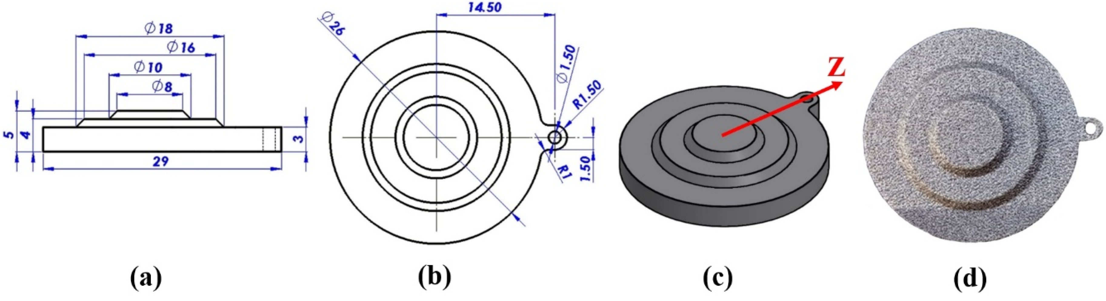
2.1. Specimens
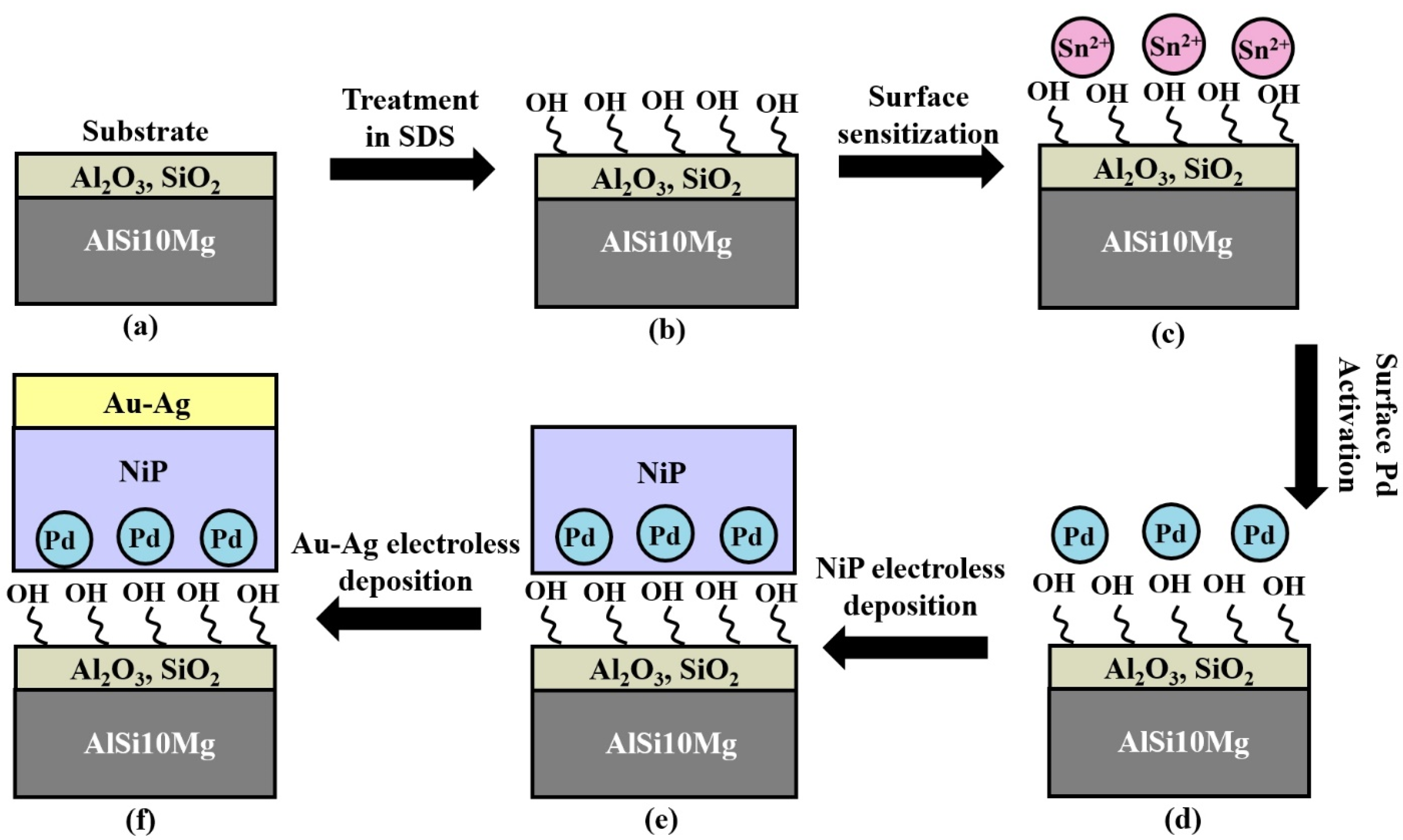
2.2. Electroless Coating of Au–Ag on Top of 3D Printed AlSi10Mg
2.3. Characterization of the Au–Ag Coating
- (a)
- A qualitative pilling test was applied to all coated specimens with transparent vinyl tape to estimate the quality of the electrum coating adhesion.
- (b)
- Optical light microscopy (Zeiss, Oberkochen, Germany) was used to observe the overall quality of the printed surface and to detect microscopic level discontinuities and defects.
- (c)
- Roughness measurements were performed with Alpha-Step D-500 Stylus Profilometer optical profilometer (OP, KLA Tencor Ltd., Milpitas, CA, USA), with 0.1 nm vertical high-resolution profiling. Average value of surface roughness (7–10 measurements) was taken into consideration.
- (d)
- The thickness of the NiP interlayer and electrum layer was measured by a calibrated high-resolution XRF (FISCHERSCOPE XRAY XDL 230, Fischer Technology Inc., Windsor, CT, USA) instrument (Table 3). The examined area in each measurement was a ~1 mm circle in diameter. Each measurement was performed for 30 s.
- (e)
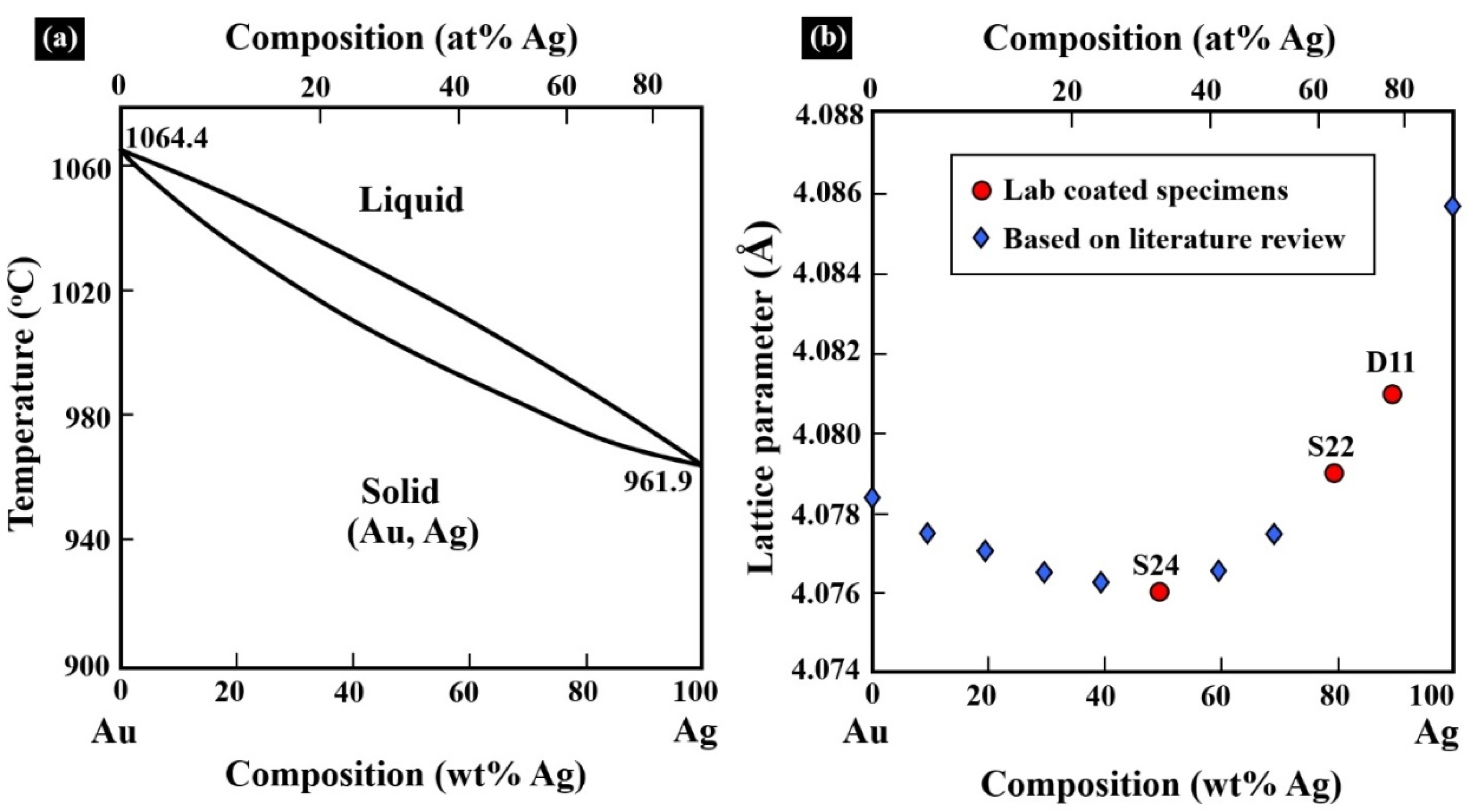
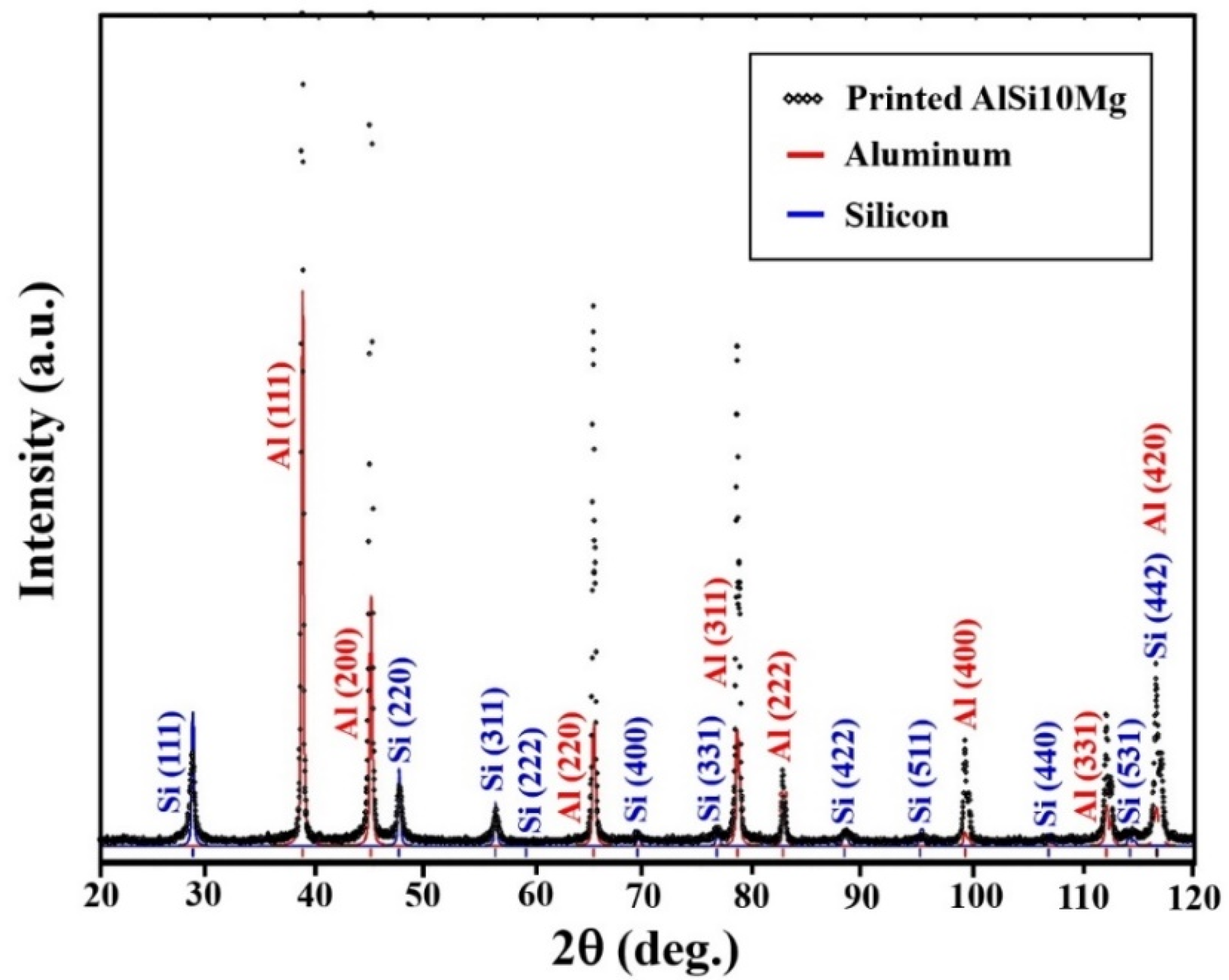
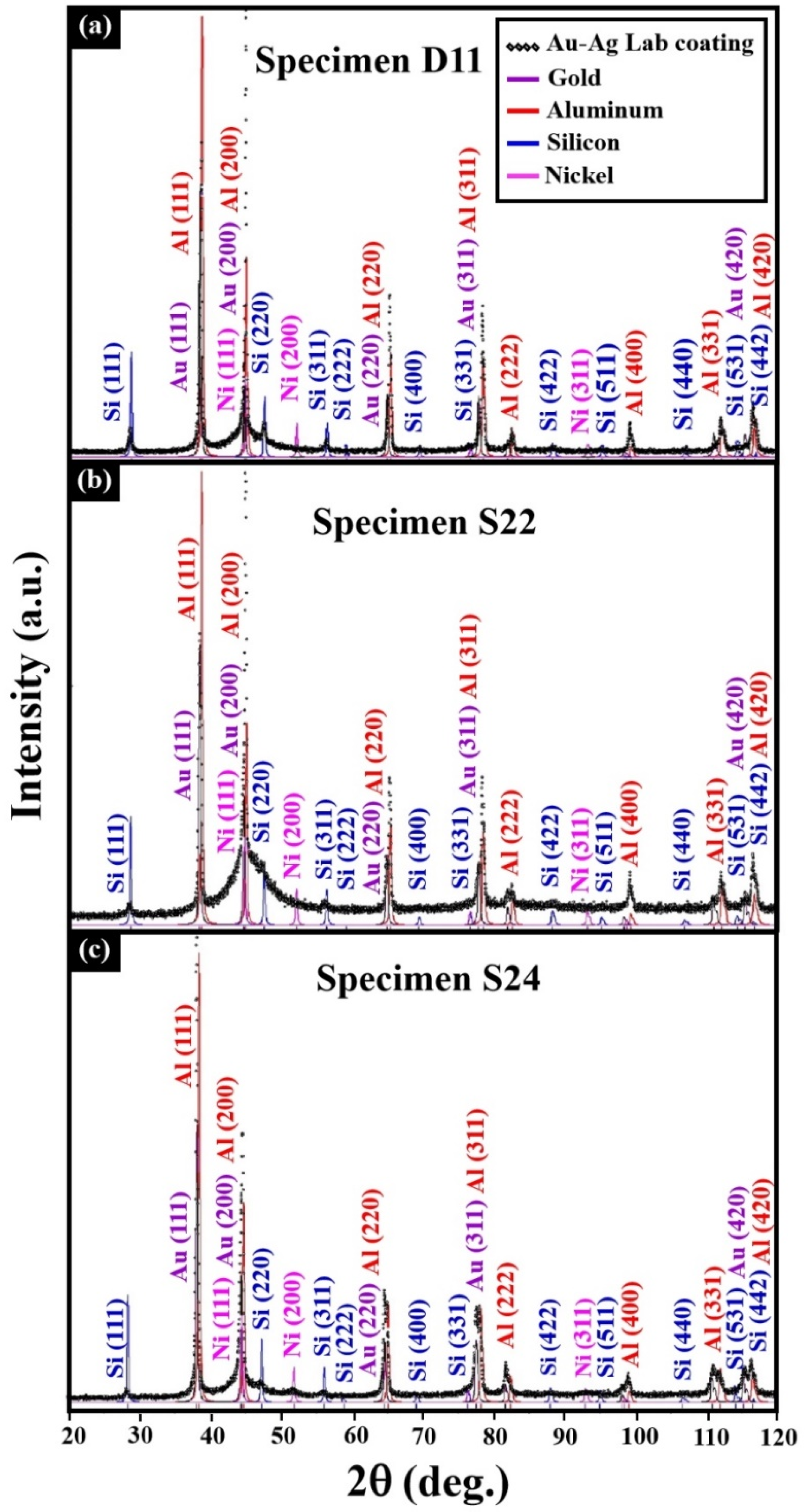
- X-ray diffraction (XRD) analysis was performed with a powder PANalytical Empyrean X-ray diffractometer (Malvern Panalytical Ltd, Malvern, UK) to determine the crystal structure of the films. Data was collected in the conventional symmetrical Bragg–Brentano configuration (θ/θ) by means of Cu Kα radiation (λ = 1.541 Å) at 40 kV and 30 mA. Phase identification from the received XRD data was made using Pearson’s handbook and ICDD data bases [47,48]. The evaluation of microstructure was done with the assistance of a Powder Cell Program [49].
- (f)
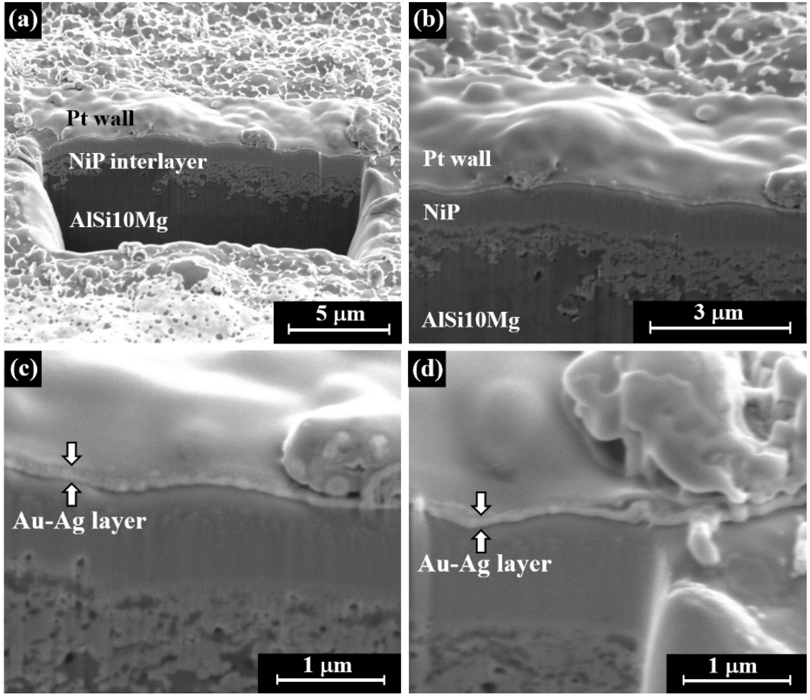
- Focused ion beam (FIB) technology was applied with machine equipped with a high-resolution scanning electron microscope (SEM) in order to detect the cross-section of the electrum-plated specimen. Before excavating into the metal layers, a platinum wall was deposited by SEM (with voltage of 2.0 kV and current of 2.7 nA). The FIB digging was performed with a high voltage of 30.0 kV and a beam current of 21.0 nA, followed by etching the wall with a beam current of 6.5 nA. The FIB’s cut dimensions are: 15 µm × 15 µm with a depth of about 7 µm.
- (g)
- X-ray photoelectron spectroscopy (XPS) measurements were performed in an ultra-high vacuum (UHV) of 2.5 × 10⁻¹⁰ Torr base pressure, using 5600 Multi-Technique System (Physical Electronics (PHI), Chanhassen, MN, USA). The specimen was irradiated with an Al Kα monochromatic source (1486.6 eV). The outcome electrons were analyzed by a spherical capacitor analyzer using the slit aperture of 0.8 mm. The specimens were not charged during measurements. The sputtering of the specimens was done using a 4 kV Ar + Ion Gun (sputter rate was 17 Å/min on SiO2/Si and was supposed to be about three times higher on Au–Ag).
3. Results and Discussion
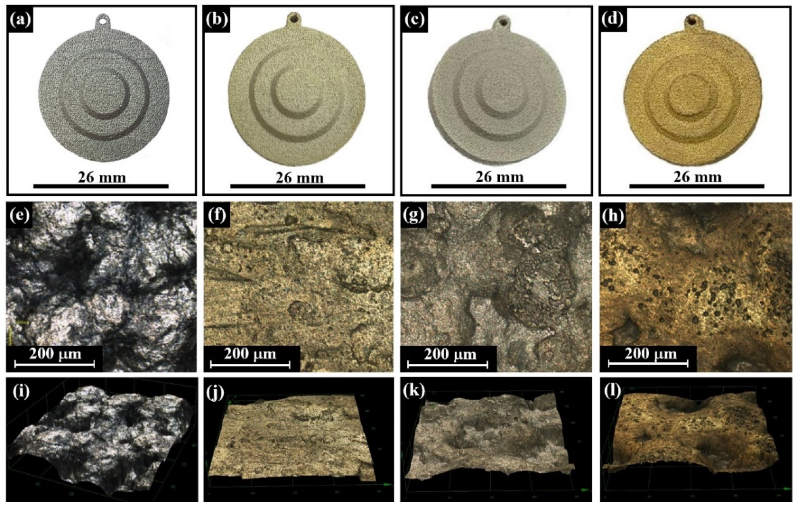
3.1. AM-LPBF AlSi10Mg Disk-Shaped Specimens
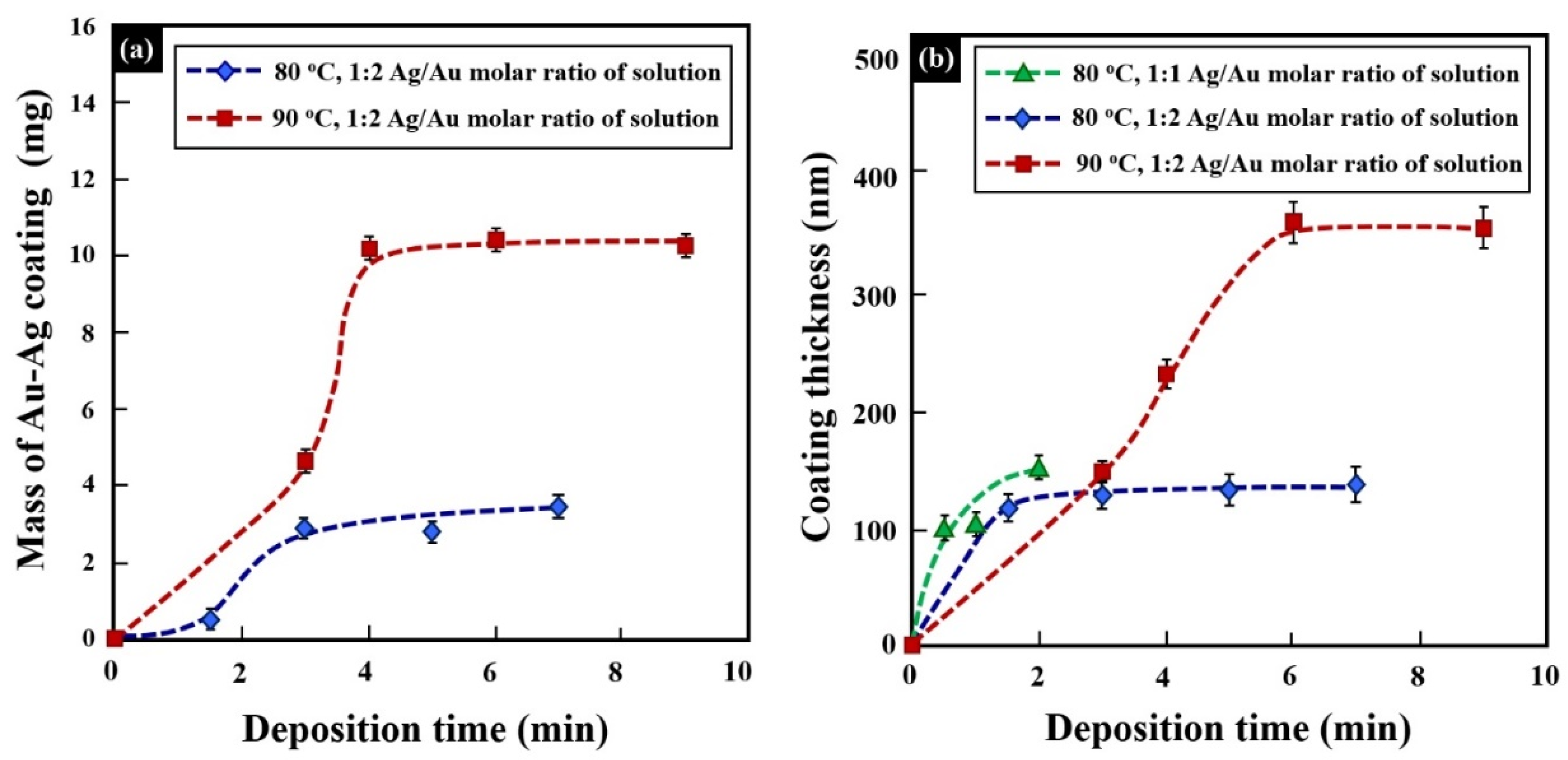
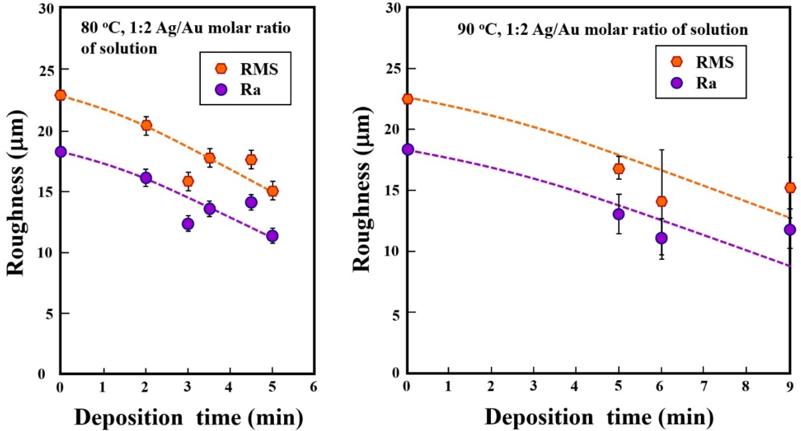
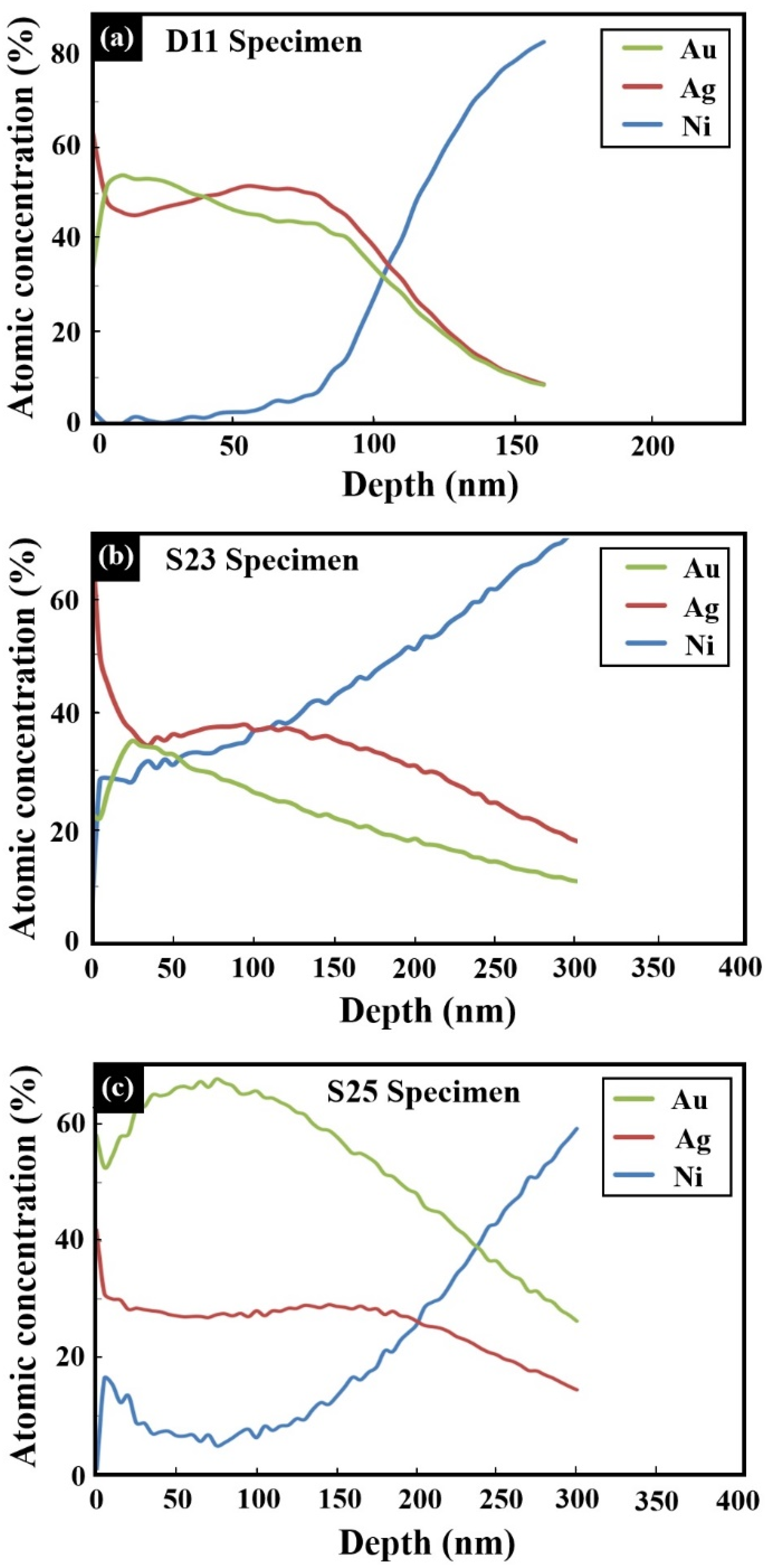
3.2. Electroless Coating of Electrum on Top of AM-LPBF AlSi10Mg Disk-Shaped Specimens
4. Conclusions
Author Contributions
Funding
Acknowledgments
Conflicts of Interest
References
- Herzog, D.; Seyda, V.; Wycisk, E.; Emmelmann, C. Additive manufacturing of metals. Acta Mater. 2016, 117, 371–392. [Google Scholar] [CrossRef]
- Steuben, J.C.; Birnbaum, A.J.; Michopoulos, J.G.; Iliopoulos, A.P. Enriched analytical solutions for additive manufacturing modeling and simulation. Add. Manuf. 2019, 25, 437–447. [Google Scholar] [CrossRef]
- Han, Q.; Gu, H.; Soe, S.; Setchi, R.; Lacan, F.; Hill, J. Manufacturability of AlSi10Mg overhang structures fabricated by laser powder bed fusion. Mater. Des. 2018, 160, 1080–1095. [Google Scholar] [CrossRef]
- Whip, B.; Sheridan, L.; Gockel, J. The effect of primary processing parameters on surface roughness in laser powder bed additive manufacturing. Int. J. Adv. Manuf. Technol. 2019, 103, 4411–4422. [Google Scholar] [CrossRef]
- Sagbas, B. Post-processing effects on surface properties of direct metal laser sintered AlSi10Mg parts. Met. Mater. Int. 2020, 26, 143–153. [Google Scholar] [CrossRef]
- Russell, R.; Wells, D.; Waller, J.; Poorganji, B.; Ott, E.; Nakagawa, T.; Sandoval, H.; Shamsaei, N.; Seifi, M. Qualification and Certification of Metal Additive Manufactured Hardware for Aerospace Applications. In Additive Manufacturing for the Aerospace Industry, 1st ed.; Froes, F., Boyer, R., Eds.; Elsevier: Amsterdam, The Netherlands, 2019; pp. 33–66. [Google Scholar]
- DebRoy, T.; Wei, H.L.; Zuback, J.S.; Mukherjee, T.; Elmer, J.W.; Milewski, J.O.; Beese, A.M.; Wilson-Heid, A.; De, A.; Zhang, W. Additive manufacturing of metallic components–process, structure and properties. Prog. Mater. Sci. 2018, 92, 112–224. [Google Scholar] [CrossRef]
- Zhang, D.; Sun, S.; Qiu, D.; Gibson, M.A.; Dargusch, M.S.; Brandt, M.; Qian, M.; Easton, M. Metal alloys for fusion-based additive manufacturing. Adv. Eng. Mater. 2018, 20, 1700952. [Google Scholar] [CrossRef]
- Hitzler, L.; Merkel, M.; Hall, W.; Öchsner, A. A review of metal fabricated with laser-and powder-bed based additive manufacturing techniques: Process, nomenclature, materials, achievable properties, and its utilization in the medical sector. Adv. Eng. Mater. 2018, 20, 1700658. [Google Scholar] [CrossRef]
- Fiegl, T.; Franke, M.; Körner, C. Impact of build envelope on the properties of additive manufactured parts from AlSi10Mg. Opt. Laser Technol. 2019, 111, 51–57. [Google Scholar] [CrossRef]
- Cabrini, M.; Lorenzi, S.; Pastore, T.; Testa, C.; Manfredi, D.; Lorusso, M.; Calignano, F.; Pavese, M.; Andreatta, F. Corrosion behavior of AlSi10Mg alloy produced by laser powder bed fusion under chloride exposure. Corros. Sci. 2019, 152, 101–108. [Google Scholar] [CrossRef]
- Kok, Y.; Tan, X.P.; Wang, P.; Nai, M.L.S.; Loh, N.H.; Liu, E.; Tor, S.B. Anisotropy and heterogeneity of microstructure and mechanical properties in metal additive manufacturing: A critical review. Mater. Des. 2018, 139, 565–586. [Google Scholar] [CrossRef]
- Cabrini, M.; Lorenzi, S.; Testa, C.; Pastore, T.; Manfredi, D.; Lorusso, M.; Calignano, F.; Fino, P. Statistical approach for electrochemical evaluation of the effect of heat treatments on the corrosion resistance of AlSi10Mg alloy by laser powder bed fusion. Electrochim. Acta 2019, 305, 459–466. [Google Scholar] [CrossRef]
- Cabrini, M.; Calignano, F.; Fino, P.; Lorenzi, S.; Lorusso, M.; Manfredi, D.; Testa, C.; Pastore, T. Corrosion behavior of heat-treated AlSi10Mg manufactured by laser powder bed fusion. Materials 2018, 11, 1051. [Google Scholar] [CrossRef] [PubMed]
- Li, B.Q.; Li, Z.; Bai, P.; Liu, B.; Kuai, Z. Research on surface roughness of AlSi10Mg parts fabricated by laser powder bed fusion. Metals 2018, 8, 524. [Google Scholar] [CrossRef]
- Maamoun, A.; Xue, Y.; Elbestawi, M.; Veldhuis, S. The effect of selective laser melting process parameters on the microstructure and mechanical properties of Al6061 and AlSi10Mg alloys. Materials 2019, 12, 12. [Google Scholar] [CrossRef]
- Shukla, S.; Gomathi, N.; George, R. Autocatalytic silver-plating of aluminum radio frequency waveguides with autocatalytic nickel as the undercoat for space applications. Surf. Topogr. Metrol. Prop. 2014, 2, 045004. [Google Scholar] [CrossRef]
- Rosenthal, I.; Shneck, R.; Stern, A. Heat treatment effect on the mechanical properties and fracture mechanism in AlSi10Mg fabricated by additive manufacturing selective laser melting process. Mater. Sci. Eng. A 2018, 729, 310–322. [Google Scholar] [CrossRef]
- Casati, R.; Hamidi Nasab, M.; Coduri, M.; Tirelli, V.; Vedani, M. Effects of platform pre-heating and thermal-treatment strategies on properties of AlSi10Mg alloy processed by selective laser melting. Metals 2018, 8, 954. [Google Scholar] [CrossRef]
- Peverini, O.A.; Addamo, G.; Lumia, M.; Virone, G.; Calignano, F.; Lorusso, M.; Manfredi, D. Additive manufacturing of Ku/K-band waveguide filters: A comparative analysis among selective-laser melting and stereo-lithography. IET Microw. Antennas Propag. 2017, 11, 1936–1942. [Google Scholar] [CrossRef]
- Dresler, N.; Inberg, A.; Ashkenazi, D.; Shacham-Diamand, Y.; Stern, A. Silver electroless finishing of selective laser melting 3D-printed AlSi10Mg artifacts. Metallogr. Microstruct. Anal. 2019, 8, 678–692. [Google Scholar] [CrossRef]
- Paunovic, M.; Schlesinger, M. Fundamentals of Electrochemical Deposition, 2nd ed.; John Wiley & Sons: Hoboken, NJ, USA, 2006; pp. 140–145. [Google Scholar]
- Asher, T.; Inberg, A.; Glickman, E.; Fishelson, N.; Shacham-Diamand, Y. Formation and characterization of low resistivity sub-100 nm copper films deposited by electroless on SAM. Electrochim. Acta 2009, 54, 6053–6057. [Google Scholar] [CrossRef]
- Inberg, A.; Livshits, P.; Zalevsky, Z.; Shacham-Diamand, Y. Electroless deposition of silver thin films on gold nanoparticles catalyst for micro and nanoelectronics applications. Microelectron. Eng. 2012, 98, 570–573. [Google Scholar] [CrossRef]
- Shacham-Diamand, Y.; Osaka, T.; Okinaka, Y.; Sugiyama, A.; Dubin, V. 30 years of electroless plating for semiconductor and polymer micro-systems. Microelectron. Eng. 2015, 132, 35–45. [Google Scholar] [CrossRef]
- Fishelson, N.; Inberg, A.; Croitoru, N.; Shacham-Diamand, Y. Highly corrosion resistant bright silver metallization deposited from a neutral cyanide-free solution. Microelectron. Eng. 2012, 92, 126–129. [Google Scholar] [CrossRef]
- Duhin, A.; Inberg, A.; Eliaz, N.; Gileadi, E. Electroless plating of rhenium-based alloys with nickel, cobalt and iron. Electrochim. Acta 2015, 174, 660–666. [Google Scholar] [CrossRef]
- Wang, J.; Wu, Q. The effects of anodic interlayer on the morphology and mechanical performances of electroless Ni–P coating on Al alloy. Appl. Phys. A 2017, 123, 435. [Google Scholar] [CrossRef]
- Szklarska-Smialowska, Z. Pitting corrosion of aluminum. Corros. Sci. 1999, 41, 1743–1767. [Google Scholar] [CrossRef]
- Marquez, K.; Staikov, G.; Schultze, J.W. Electrochemical deposition of Ag, Au and Ag–Au alloys on Si(111). Trans. IMF 2002, 80, 73–78. [Google Scholar] [CrossRef]
- Huang, T. Electrodeposited silver-gold alloys as a sensor for paracetamol determination. Int. J. Electrochem. Sci. 2017, 12, 11419–11427. [Google Scholar] [CrossRef]
- Akben, K.; Timur, S. A study of gold–silver alloy electrodeposited from pyrophosphate-cyanide electrolyte using polyethylenimine-KSeCN additives. Int. J. Electrochem. Sci. 2018, 13, 3855–3873. [Google Scholar] [CrossRef]
- Link, S.; Wang, Z.L.; El-Sayed, M.A. Alloy formation of gold–silver nanoparticles and the dependence of the plasmon absorption on their composition. J. Phys. Chem. B 1999, 103, 3529–3533. [Google Scholar] [CrossRef]
- Shibata, T.; Bunker, B.A.; Zhang, Z.; Meisel, D.; Vardeman, C.F.; Gezelter, J.D. Size-dependent spontaneous alloying of Au–Ag nanoparticles. J. Am. Chem. Soc. 2002, 124, 11989–11996. [Google Scholar] [CrossRef] [PubMed]
- Liu, S.; Chen, G.; Prasad, P.N.; Swihart, M.T. Synthesis of monodisperse Au, Ag, and Au–Ag alloy nanoparticles with tunable size and surface plasmon resonance frequency. Chem. Mater. 2011, 23, 4098–4101. [Google Scholar] [CrossRef]
- Zhang, Q.; Jing, H.; Li, G.G.; Lin, Y.; Blom, D.A.; Wang, H. Intertwining roles of silver ions, surfactants, and reducing agents in gold nanorod overgrowth: Pathway switch between silver underpotential deposition and gold–silver codeposition. Chem. Mater. 2016, 28, 2728–2741. [Google Scholar] [CrossRef]
- Ahn, J.; Wang, D.; Ding, Y.; Zhang, J.; Qin, D. Site-selective carving and co-deposition: Transformation of Ag nanocubes into concave nanocrystals encased by Au–Ag alloy frames. ACS Nano 2018, 12, 298–307. [Google Scholar] [CrossRef]
- Okamoto, H.; Massalski, T.B. The Ag–Au (silver-gold) system. Bull. Alloy Phase Diagr. 1983, 4, 30–38. [Google Scholar] [CrossRef]
- Ashkenazi, D.; Gitler, H.; Stern, A.; Tal, O. Archaeometallurgical characterization and manufacturing technologies of fourth century BCE silver jewelry: The Samaria and Nablus hoards as test case. Metallogr. Microstruct. Anal. 2018, 7, 387–413. [Google Scholar] [CrossRef]
- Bond, G.C.; Thompson, D.T. Catalysis by gold. Catal. Rev. 1999, 41, 319–388. [Google Scholar] [CrossRef]
- Krupp, R.E.; Weiser, T. On the stability of gold–silver alloys in the weathering environment. Miner. Depos. 1992, 27, 268–275. [Google Scholar] [CrossRef]
- Lubarda, V.A. On the effective lattice parameter of binary alloys. Mech. Mater. 2003, 35, 53–68. [Google Scholar] [CrossRef]
- Elliott, R.P.; Shunk, F.A. The Ag–Au (silver-gold) system. Bull. Alloy Phase Diagr. 1980, 1, 45–47. [Google Scholar] [CrossRef]
- Hough, R.M.; Butt, C.R.; Fischer-Bühner, J. The crystallography, metallography and composition of gold. Elements 2009, 5, 297–302. [Google Scholar] [CrossRef]
- Troalen, L.G.; Tate, J.; Guerra, M.F. Goldwork in Ancient Egypt: Workshop practices at Qurneh in the 2nd Intermediate Period. J. Archaeol. Sci. 2014, 50, 219–226. [Google Scholar] [CrossRef]
- Guisbiers, G.; Mendoza-Cruz, R.; Bazán-Díaz, L.; Velázquez-Salazar, J.J.; Mendoza-Perez, R.; Robledo-Torres, J.A.; Rodriguez-Lopez, J.L.; Montejano-Carrizales, J.M.; Whetten, R.L.; José-Yacamán, M. Electrum, the gold–silver alloy, from the bulk scale to the nanoscale: Synthesis, properties, and segregation rules. ACS Nano 2015, 10, 188–198. [Google Scholar] [CrossRef] [PubMed]
- File, P.D. Powder Diffraction Data; International Centre for Diffraction Data: Newtown Square, PA, USA, 1986. [Google Scholar]
- Villard, P.; Calvert, L.D. Pearson’s Handbook of Crystallographic Data for Intermetallic Phases; American Society for Metals: Cleveland, OH, USA, 1985. [Google Scholar]
- Kraus, W.; Nolze, G. Power Cell—A program for the representation and manipulation of crystal structures and calculation of the resulting X-ray powder patterns. J. Appl. Crystallogr. 1996, 29, 301–303. [Google Scholar] [CrossRef]
- Reiher, T.; Lindemann, C.; Jahnke, U.; Deppe, G.; Koch, R. Holistic approach for industrializing AM technology: From part selection to test and verification. Prog. Addit. Manuf. 2017, 2, 43–55. [Google Scholar] [CrossRef]
- Boschetto, A.; Bottini, L.; Veniali, F. Roughness modeling of AlSi10Mg parts fabricated by selective laser melting. J. Mater. Proc. Technol. 2017, 241, 154–163. [Google Scholar] [CrossRef]
- Frenkel, A.I.; Machavariani, V.S.; Rubshtein, A.; Rosenberg, Y.; Voronel, A.; Stern, E.A. Local structure of disordered Au-Cu and Au–Ag alloys. Phys. Rev. B 2000, 62, 9364. [Google Scholar] [CrossRef]
- Younes, O.; Zhu, L.; Rosenberg, Y.; Shacham-Diamand, Y.; Gileadi, E. Electroplating of amorphous thin films of tungsten/nickel alloys. Langmuir 2001, 17, 8270–8275. [Google Scholar] [CrossRef]
- Sade, W.; Proença, R.T.; Moura, T.D.D.O.; Branco, J.R.T. Electroless Ni–P coatings: Preparation and evaluation of fracture toughness and scratch hardness. ISRN Mater. Sci. 2011, 1–6. [Google Scholar] [CrossRef]
- Sudagar, J.; Lian, J.; Sha, W. Electroless nickel, alloy, composite and nano coatings—A critical review. J. Alloy. Compd. 2013, 571, 183–204. [Google Scholar] [CrossRef]
- Rajabalizadeh, Z.; Seifzadeh, D. The effect of copper ion on microstructure, plating rate and anticorrosive performance of electroless Ni–P coating on AZ61 magnesium alloy. Prot. Met. Phys. Chem. Surf. 2014, 50, 516–523. [Google Scholar] [CrossRef]
- Inberg, A.; Bogush, V.; Croitoru, N.; Dubin, V.; Shacham-Diamand, Y. Novel highly conductive silver-tungsten thin films electroless deposited from benzoate solution for microelectronic applications. J. Electrochem. Soc. 2003, 150, C285–C291. [Google Scholar] [CrossRef]
- Linstrom, P.J.; Mallard, W.G. NIST Chemistry WebBook: NIST Standard Reference Database Number 69; NIST: Gaithersburg, MD, USA, 2003. [Google Scholar]
- Luo, Y.R.; Kerr, J.A. Bond Dissociation Energies. In CRC Handbook of Chemistry and Physics; CRC Press: Boca Raton, FL, USA, 2010; p. 89. Available online: https://notendur.hi.is/agust/rannsoknir/papers/2010-91-CRC-BDEs-Tables.pdf (accessed on 1 January 2019).


| Component | Concentration (g/l) |
|---|---|
| NiSO4·6H2O | 30 |
| NaCH3COO | 5 |
| 3-Na-citrate | 12.6 |
| NaH2PO2 | 10 |
| Component | Concentration |
|---|---|
| KAu(CN)2 | 7 mM |
| KAg(CN)2 | 3.5 mM |
| 3-Na-citrate (3Na3C6H5O7) | 170 mM |
| Hydrazine hydrate | 15 mM |
| PEG 1500 | 0.5 g/l |
| Sodium saccharin | 0.5 g/l |
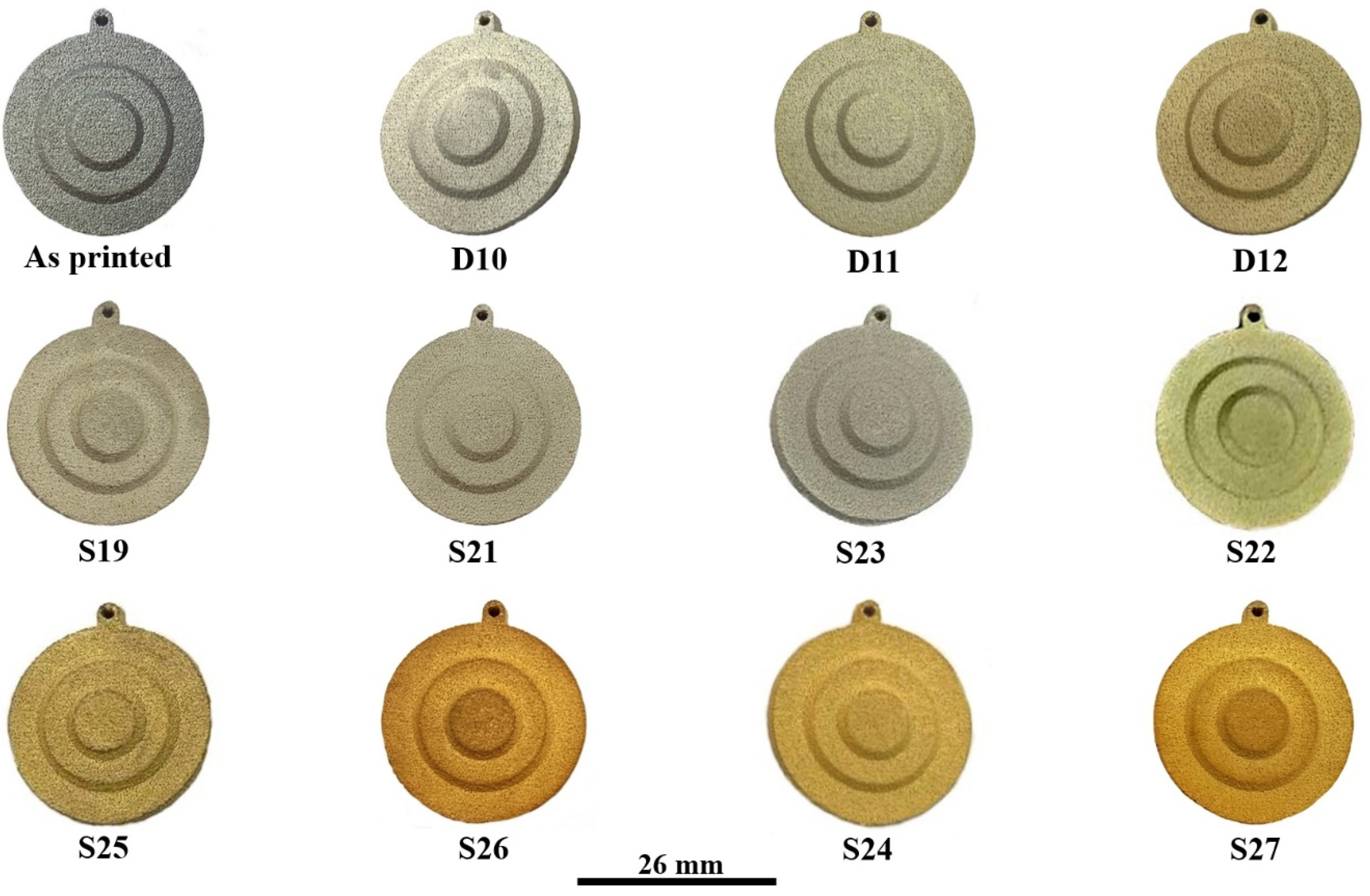
| Specimen No. | Ag/Au Molar Ratio of Solution | ELD Temperature (°C) | ELD Time (min) | Average Thickness (µm) XRF Measurement | |
|---|---|---|---|---|---|
| NiP Interlayer | Au–Ag Layer | ||||
| D12 | 1:1 | 80 | 0.5 | 2.6 | 0.10 |
| D11 | 1:1 | 80 | 1 | 2.3 | 0.11 |
| D10 | 1:1 | 80 | 2 | 3.1 | 0.15 |
| S19 | 1:2 | 80 | 1.5 | 5.7 | 0.12 |
| S21 | 1:2 | 80 | 3 | 5.7 | 0.13 |
| S23 | 1:2 | 80 | 5 | 5.4 | 0.13 |
| S22 | 1:2 | 80 | 7 | 5.7 | 0.14 |
| S25 | 1:2 | 90 | 3 | 4.1 | 0.15 |
| S26 | 1:2 | 90 | 4 | 4.7 | 0.23 |
| S24 | 1:2 | 90 | 6 | 4.2 | 0.36 |
| S27 | 1:2 | 90 | 9 | 4.8 | 0.36 |
| Specimen | Lattice Parameter (Å) | Characteristics of the Electrum (Au–Ag) Coating | Characteristics of the Ni–P Interlayer | Characteristics of the Printed Substrate |
|---|---|---|---|---|
| D11 | 4.080 (±0.001) | Rich in Ag, solid-solution crystalline phase | Quasi-amorphous | Major crystalline phase Al Minor crystalline phase Si |
| S22 | 4.079 (±0.001) | |||
| S24 | 4.076 (±0.001) | Rich in Au, solid-solution crystalline phase | Mix of quasi-amorphous and nanocrystalline |
© 2020 by the authors. Licensee MDPI, Basel, Switzerland. This article is an open access article distributed under the terms and conditions of the Creative Commons Attribution (CC BY) license (http://creativecommons.org/licenses/by/4.0/).
Share and Cite
Inberg, A.; Ashkenazi, D.; Kimmel, G.; Shacham-Diamand, Y.; Stern, A. Gold–Silver Electroless Plating on Laser Powder-Bed Fusion Additively Printed AlSi10Mg Parts. Metals 2020, 10, 557. https://doi.org/10.3390/met10050557
Inberg A, Ashkenazi D, Kimmel G, Shacham-Diamand Y, Stern A. Gold–Silver Electroless Plating on Laser Powder-Bed Fusion Additively Printed AlSi10Mg Parts. Metals. 2020; 10(5):557. https://doi.org/10.3390/met10050557
Chicago/Turabian StyleInberg, Alexandra, Dana Ashkenazi, Giora Kimmel, Yosi Shacham-Diamand, and Adin Stern. 2020. "Gold–Silver Electroless Plating on Laser Powder-Bed Fusion Additively Printed AlSi10Mg Parts" Metals 10, no. 5: 557. https://doi.org/10.3390/met10050557
APA StyleInberg, A., Ashkenazi, D., Kimmel, G., Shacham-Diamand, Y., & Stern, A. (2020). Gold–Silver Electroless Plating on Laser Powder-Bed Fusion Additively Printed AlSi10Mg Parts. Metals, 10(5), 557. https://doi.org/10.3390/met10050557