Article

Gallium Nitride Inverter Design with Compatible Snubber Circuits for Implementing Wireless Charging of Electric Vehicle Batteries

by
Fatemeh Rahmani
,
Payam Niknejad
,
Tanushree Agarwal
and
Mohammadreza Barzegaran
*
Department of Electrical Engineering, Lamar University, Beaumont, TX 77710, USA
*
Author to whom correspondence should be addressed.
Machines 2020, 8(3), 56; https://doi.org/10.3390/machines8030056
Submission received: 12 August 2020 / Revised: 8 September 2020 / Accepted: 12 September 2020 / Published: 15 September 2020

Abstract

:
High-frequency wireless power transfer (WPT) technology provides superior compatibility in the alignment with various WPT standards. However, high-efficiency and compact single-phase power switching systems with ideal snubber circuits are required for maximum power transfer capability. This research aims to develop an inverter using Gallium Nitride (GaN) power transistors, optimized RCD (resistor/capacitor/diode) snubber circuits, and gate drivers, each benefitting WPT technology by reducing the switching and conduction loss in charging electric vehicle batteries. A full-bridge GaN inverter was simulated and instituted as part of the wireless charging circuit design. The RCD circuits were adjusted by transferring maximum power from the power supply to the transmitter inductor. For verification of the simulated output, lab-scale experiments were implemented for two half-bridges controlled by gate drivers with corresponding snubber circuits. After authenticating the output results, the GaN inverter was tested with an input range of 30 V to deduce the success of charging electric vehicle batteries within an efficient time frame. The developed inverter, at 80 kHz frequency, was applied in place of a ready-to-use evaluation board, fully reducing less harmonic distortion and greatly increasing WPT system efficiency (~93%). In turn, the designed GaN inverter boasts considerable energy savings, resulting in a more cost-effective solution for manufacturers.

1. Introduction

1.1. Motivation

Gallium Nitride (GaN) power switches were selected because of their reasonable prices, higher efficiency, maximum power density, and outstanding reliability. Commercially available GaN transistors are developed by various manufacturers, namely Efficient Power Conversion (EPC), Panasonic, and Transphorm. While prior studies [1,2,3,4,5] evinced that a high-frequency H-bridge GaN inverter with compact size, lower-price, and high-performance is rarely found in the market, this project was designed to fulfill the indicated demand. Previously, scientists have designed GaN inverters using the dual-frequency programmed harmonic modulation method at ~26–991.6 kHz with totem-pole rectifiers operating in a discontinuous conduction mode at 6.78 MHz [6,7]. However, in this article, the proposed GaN inverter with optimized snubber circuits at 80 kHz reduces the size of the overall system design, and minimizes the associated cost of installation and maintenance for wireless charging of electric vehicle batteries. Aiming to limit harmonic content in the output waveform, this research specifically introduced the H-bridge GaN inverter operating with pulse-width-modulation (PWM). Thus, the PWM signal to the Silicon Labs gate drivers converts the undesired frequency content to the switching frequency (80 kHz).

1.2. Literature Review

Latest evaluations of wireless power transfer (WPT) technologies require high-efficiency power converters. High-power converters possess the capability to charge the battery wirelessly in static and dynamic charging technologies [8,9]. Considering the fast advancement of high-frequency converters and the resulting boom in modern machinery, this charging technology is critical for electric vehicles (EVs). While the operating frequency ranges from tens of kilohertz to several megahertz, increasing the frequency for the WPT in electric vehicles extends the wireless power distance, decreases cost, and reduces the size of the coupling circuit design [10]. High-stress voltage and power rate limitations of the high-frequency switching components presents complexities in maximizing the output power of the WPT system. Therefore, applying half/full-bridge inverters allows the output power to reach the maximum level safely [8,11].
High-frequency WPT applications lead to an increased loss on semiconductor switching devices, which may adversely affect comprehensive system efficiency. Several of these power electronics issues can be resolved in the following ways.
The first solution rests in applying wide-bandgap (WBG) devices, particularly a GaN heterojunction field effect transistors (HFETs), to design the electrical inverters [12,13]. GaN transistors with superior features and small input/output capacitance (CGS+CGD) reduce losses for WPT converters at the kilohertz band frequency with a lower gate charge (QG). Additionally, the reduction of switching device losses warrants the utilization of lower-cost heat dissipation components to charge the EV batteries [14]. While silicon carbide (SiC) transistor technology has been the most heavily used for several decades due to a maximum critical breakdown field and thermal conductivity features with wider bandgap, GaN transistors with increased efficiency are steadily popularising [15]. Lower parasitic losses, high electron mobility, and a high-temperature coefficient in the GaN layout promise faster switching transistors, optimized PWM resolution, less harmonic distortion, and higher power density compared to silicon or silicon carbide power transistors for eventual power conversion applications. Although GaN switches perform at an accelerated rate when smaller in size, they are sensitive to the layout area and slightly more costly than SiC transistors. The outstanding performance of the GaN transistor’s gate driver enables high-frequency operation with straightforward and accessible snubber configuration and passive filter components [16,17,18,19]. Controlling the GaN FET with a gate driver is similar to the function of a nonlinear capacitor. Charging the gate capacitor turns the power device on and allows current flow through its drain and source terminations. For operating a GaN switch, a voltage sufficiently larger than VTH, the minimum voltage required to charge the gate capacitor, should be applied between the gate and source of a transistor [20]. The lab-scale simulation and implementation of the GaN inverter and its gate driver have to follow the approved standard to utilize their design on a global scale. SAE J2954 and SAE J1772 are well-known standards of industry guidelines for establishing wireless power transfer between infrastructures, vehicle suppliers, and original equipment manufacturers for light-duty EVs. Applied in all light-duty vehicle systems, a common frequency band according to SAE J2954 is ~85 kHz, and 80 kHz for SAE J1772. In addition, the four classes of wireless power transfer levels for the above standards are defined as 3.7 kW, 7.7 kW, 11 kW, and 22 kW [21]. In this study, the simulated WPT system with an invented single-phase GaN inverter was constructed considering the characteristics of the existing GaN transistor and its gate driver in the industrial marketplaces. Thus, this project aims to meet SAE J1772 standard by isolated AC-DC stage, cost-optimized converters, and linear regulators at ~80 kHz to achieve ENERGY STAR® certification for EV charging stations [22]. Next, this research provides answers for the following queries: How does a full-bridge GaN inverter play a major role in the wireless charging of EV batteries? Further, which parameters are particularly essential for designing the single-phase inverter using GaN switches?
Secondly, employing the active and passive snubber or energy absorbing circuits reduces voltage spikes [5]. Voltage spikes occur when the parasitic capacitance of the inductors and the junction capacitance of the rectifier converts the resonance to leakage inductance. To address this issue in the WPT system, it is imperative that the snubber circuits are adjusted, improving the output voltage and current waveforms, providing opportunities for EV charging applications [23,24]. Other advantages include the reduction of the electromagnetic interference (EMI) and power dissipation of WPT circuits [25]. In spite of designing the snubber circuit, in order to obtain the high-efficiency output, the series-series (SS) compensation circuits should be attached to the transmitter/receiver magnetic coupling, allowing them to resonate at the same frequency. When the WPT system operates at the resonant frequency, the capacitive compensator reduces the transmitter reactive power (Q) of power source and increases receiver power transfer (PT) to charge the car battery [26]. This study proposed SS compensation capacitors for magnetic transmitter/receiver and resistor, capacitor, and diode (RCD) snubber circuits for GaN inverter and rectifiers to boost the power efficiency, minimize the voltage spikes, and improve the output system waveforms.
However, this research addressed the shortcomings presented in former studies, namely, overcoming higher conduction and switching losses by implementing neutral point clamping, low operating switching frequencies, narrow-bandgap, low electron mobility, excessive thermal conductivity, being susceptible to noise, and overpriced inverter execution.

1.3. Contributions

This paper demonstrates an H/full-bridge inverter, implemented by GaN power switches, operating at a high-frequency of 80 kHz based off of the SAE J1772 standard for wireless charging of EV batteries. This finding proves that on a real-world scale, the proposed GaN inverter configuration will remarkably exhibit perfect output in terms of power density and efficiency (~93%), contrary to Si-based power inverters. Moreover, applying the simulated and adjusted RCD snubber circuits for each inverter’s half-bridge boosts efficiency and output power. All simulated results were tested in lab-scale experiments to verify that the invented GaN inverter will be overwhelmingly applicable in the wireless charging of electric vehicle batteries, as well as highly effective in prospective WPT system implementations.
More specifically, the acquired methodological technique was carried out in four objectives:
First objective: Simulating the H/full-bridge inverter, consisting of GaN transistors, at 80 kHz, along with compatible and optimized RCD snubber circuits for each half-bridge (Section 2).
Second objective: Simulating power supply, transmitter/receiver coils and rectifiers, and battery of the WPT system followed by overall system testing via the designed GaN inverter (Section 2).
Third objective: Comparing designed wireless charging systems with/without snubber circuits in the simulated and experimental results (Section 3.1 and Section 3.2).
Final objective: Authenticating all objectives through experimental lab-tested results, anticipating that the innovative design of the high-frequency GaN inverter with ideal snubber circuits in a compact size is lucrative in EV applications (Section 3.3).

2. System Design and Modeling

2.1. Methods and Materials

This section explains the employed methods and materials behind the designed wireless charging system using copper transmitter and receiver coils. The mentioned circuit will eliminate the need to plug-in when charging electric vehicle batteries. In this project, an advanced method is utilized at a high-frequency via a full-bridge GaN inverter and corresponding snubber circuits to improve output results, enabling a consistent AC signal to be delivered to the transmitter coil. Though the simulation is functional at a higher voltage and with increased current, the Microgrid Lab presented voltage/current limitations for the components. Therefore, the project was designed and tested with variable voltage, around 30 V (VP–P).
The proposed WPT system transferred 100 W of power across a pair of circular coils with a 0.63 coupling coefficient and Ferrite cores placed under the transmitter coil and on the top of the receiver coil. The outer diameter is 32.26 cm, and the inner diameter is 10.76 cm for the transmitter/receiver coils. The inverter switches in this system are TPH3006PS GaN FETs from Transphorm Inc. and two Si8231AB-1616DFL073 gate drivers from Silicon Labs. The rectifier diodes are F1E35AA-R1560G2, 0.8 V Schottky diodes. The rest of the method description and component characteristics will be thoroughly addressed in further subsections.

2.2. Simulated Wireless Charging Circuit with GaN Inverter

As mentioned above, the final objective of this research is to charge EV batteries wirelessly using the innovative GaN inverter, which was simulated in ANSYS Simplorer and MATLAB Simulink. Figure 1a exhibits detailed internal connections of the designed full-bridge GaN inverter with their gate controllers that optimize the AC voltage at high-frequency for the transmitter inductor. The gate driver for each half-bridge is designed with 16 pin connections to transfer the input PWM signal from Analog Discovery to the transistor gates. These gate controllers are fed by 5 VDC and 7.2 VDC supplies.
Moreover, Figure 1b depicts the second portion of the wireless charging circuit, including the receiver coil, the receiver rectifier, and the battery. Table 1 also displays the specifications of the wireless charging components.
According to Figure 1a and Figure 2, the transmitter rectifier converts the supplied 30 VAC (green waveform) to 28 VDC (red waveform), which is then transferred to the full-bridge GaN inverter. The efficiency of the designed GaN inverter is ~93%, proving that all selected components were simulated accurately to obtain the maximum output voltage to transfer to the receiver coil underneath the electric car. Accordingly, the battery is charged in an efficient time.
As depicted in Figure 1b and Figure 3, the receiver coil wirelessly transfers AC voltage (red waveform) from the transmitter coil to the receiver rectifier in order to charge the 336 W (48 V) battery. The receiver coil receives 21 V of the 28 V supplied from the transmitter coil. Voltage reduction emerges due to power loss from nonconductive mediums, such as air between the transmitter coil in the ground and the receiver coil underneath the EV. Figure 4 illustrates that the battery with 5 V initial voltage can be charged 0.19 V in 9 s. Consequently, the designed WPT system charges the 48 V battery in ~39 min, which is precisely the optimum amount of time needed to charge the lab-scale EV battery.

2.3. Optimization of Snubber Circuits for Simulated GaN Inverter

Optimized snubber circuits of a GaN inverter have a crucial role in charging a car battery. Without an intrinsic body diode, GaN switches have zero recovery, yet, IGBT transistors are still required to apply anti-parallel diodes. Hence, GaN transistors are naturally capable of reversing conduction, indicating that various characteristics depend on the voltage of the transistor gate without any anti-parallel diodes [27]. According to this specific feature of the GaN switches, the proposed snubber circuit should be designed with a diode connected in parallel to the snubber elements, rather than the GaN transistor, to achieve the desirable receiver current. This project consequently applied the resistor and diode, connected in parallel, in conjunction with the capacitor design, connected in series, for designing the GaN inverter.
Leakage inductance between transmitter and receiver inductors is a significant concern in various types of inverter structures, specifically because the parasitic capacitance of the inductors and junction capacitance of the rectifier initiates leakage inductance causing voltage spikes. Leakage inductance, shown in Equation (1), clarifies why optimized RCD snubber circuits should be added to each switch of the inverter, to remove spikes from output power waveforms [5].
L L K ( H ) = μ 0 N 2 L w M 2 B w [ 1 3 h p + h Δ ]
where N is the number of turns, μ 0   ( H m ) is the permeability of air surrounding the conductors, M   ( H ) is the mutual inductance, L w   ( m ) is the coil length, B w   ( m m ) is the breadth of winding, h p   ( m m ) is the height of pth winding, and h Δ   ( m m ) is the distance between the transmitter and receiver inductors.
With the goal of decreasing the leakage inductance ( L L K ) and voltage spikes, this project designed and attached snubber circuits to the GaN inverter to increase M and B w in Equation (1). Hence, according to Table 1, the leakage inductance values were compared in the wireless charging circuit system with and without snubber circuits through ANSYS Maxwell. Applying the snubber circuits incredibly reduced leakage inductance from 100 nH to a final value of 1 nH for the overall system.
On the other hand, when the GaN switches in Figure 1a experience great amounts of stress, from functioning at a high-frequency, increased power dissipation is generated. Compatible snubber circuits provide the solution for minimizing power dissipation in the wireless charging system while controlling the peak current of the switches in the inverter. The power dissipation value was acquired from Equation (2) and Table 1, which is inversely related to the output current ( I O ) . In other words, when the snubber circuits are added, ( I O ) increases, and a reduction of power dissipation ( P d i s s ) occurs. In this research, after applying the snubber circuits to the inverter, the power dissipation of the WPT system (Figure 1) was reduced from 2 mW to 0.8 mW.
P d i s s ( W ) = ( N I O + 1 2 N ) × V i n V d i s s × π 2 C I ( L 1 + L 2 ) I i n I O 2 N + 2 L 2 L 1 × I i n cos ( 2 π f t ) I
where N is the number of turns, L 1   ( H ) and L 2   ( H ) are the transmitter/receiver inductances, V i n   ( V ) and I i n   ( A ) are the input voltage and current, C I   ( F ) is the input capacitance, f   ( H z ) is the switching frequency, and t   ( s ) is the battery charging time.
The remaining of this section discusses how the RCD snubber circuits were optimized to reduce voltage spikes, prevent overheating, and increase the overall system efficiency. This project applied the optimization Bubble Sort algorithm to determine the ideal capacitance and resistance at a high inverter efficiency, ~93%. In addition, the same snubber circuits were simulated for all of the GaN transistors in the inverter. In order to achieve 93% inverter efficiency with minimum loss, the resistance range of 530–560 Ω and capacitance range of 150–250 PF with 0.8 mW power dissipation was determined, as presented in Figure 5.
After discovering the resistance range, the inverter, coils, and rectifier efficiencies were confirmed for the wireless charging of EVs, highlighted in Figure 6. Those efficiencies displayed their maximum values in the resistance range of 545–560 Ω. Therefore, the achieved resistance value in Figure 5 was verified and applied in the WPT system shown in Figure 1.
Lastly, the RCD snubber circuit was subsequently instituted in the GaN inverter circuit to investigate the effects of the designed snubber circuits on output simulated results. Figure 7 demonstrates that the designed snubber circuits in this research eliminate AC voltage spikes in the waveform output of the GaN inverter.

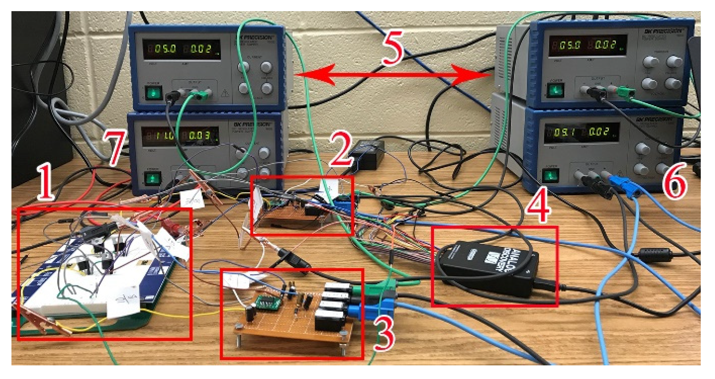
3. Experimental Process

Three processes are comprehensively defined for the implementation of the GaN inverter. As the project progressed, each step had to be meticulously checked for accuracy. All courses of action will be further explained below, along with the experimental results.

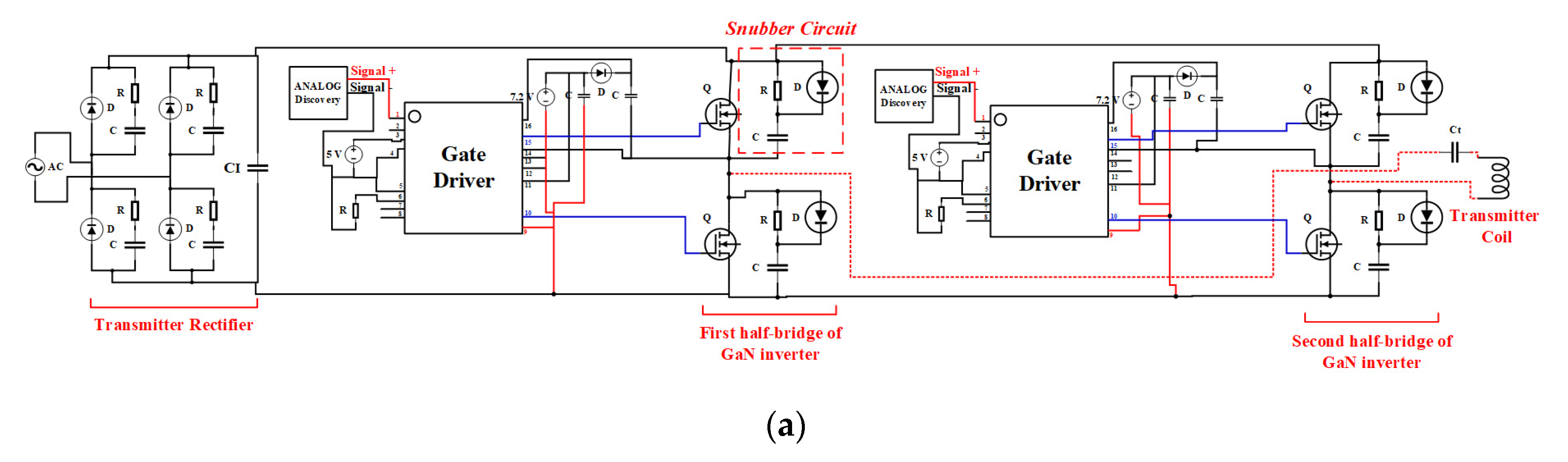
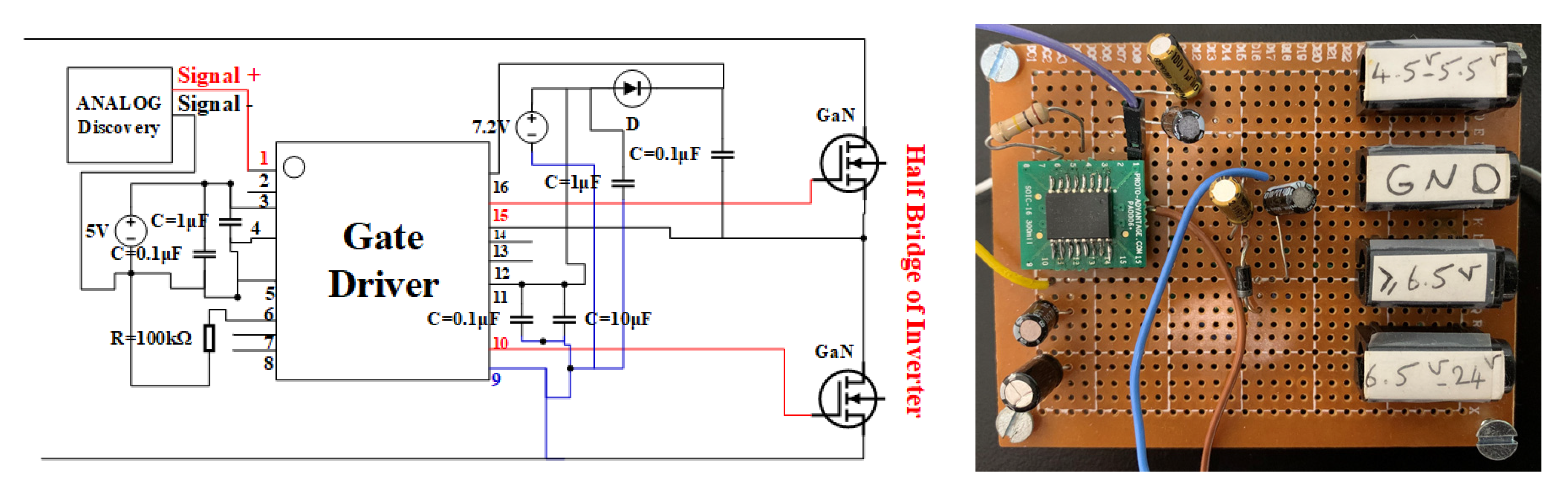
3.1. Full-Bridge GaN Inverter without Snubber Circuits—Experimental Tests and Results

Putting the GaN inverter into experimental practice proved to be much more complex than the simulation circuits. The PWM from the simulation section was already defined in the software and did not require a particular corresponding inverter transistor model. However, the experimental testing of the full-bridge GaN inverter necessitates an individually matched gate driver for each switch. Hence, this issue was addressed by contacting the manufacturing specialists.
In this experiment, four TPH3006PS GaN transistors from Transphorm Inc. and two Si8231AB-1616DFL073 gate drivers from Silicon Labs were purchased to construct an H/full-bridge GaN inverter. Two gate drivers were implemented based on the spec sheet to control each half-bridge of the inverter, as illustrated in Figure 8. Afterward, output results of the half-bridges were checked for inverse signals (ON/OFF), which were sent in-turn to the GaN switches. As displayed in Figure 1, both gate drivers applied in the full-bridge inverter circuit possess identical designs, were executed identically, and proved identical outcomes. Thus, only one of the gate drivers will continue to be discussed for the remainder of this section.
The following significant points were considered for connecting the above gate driver model to the switches:
  • The ultra-fast diode (D) fed by 7.2 VDC with high-breakdown voltage must be able to withstand the DC bus voltage.
  • A low capacitance value is crucial for connection to the diode because the capacitor must generate low voltage to initiate a gate signal without any startup delay.
  • Pins 1–8 of the gate driver are supplied by exactly 5 V, and pins 9–16 are fed by > 7.2 V (9.1 V in this project).
Before sending the signal to the inverter, the gate drivers were checked individually in order to confirm their output signals. According to Figure 9, the yellow signals demonstrate gate driver input received from Analog Discovery, and the blue signals show the high/low-level signals of the gate driver output at 79.62 kHz that control the top and bottom transistors of the half-bridge GaN inverter. In other words, when the gate driver received +/− pulses from Analog Discovery, it generated a signal identical to the original input when in “ON” mode, along with an inverse signal when in “OFF” mode. Figure 9 proves that the experimental gate drivers were ideally implemented because the acquired output signal mirrored the simulated pulse wave.
According to Figure 10, all output results of the gate drivers were validated, as previously explicated, and the full-bridge GaN inverter was then analyzed with both gate drivers. The implemented inverter with no designed snubber circuits converted VDC to VAC (11.15 V) and included some spikes, as delineated in Figure 11. This inverter required modification. Compatible snubber circuits were added to prevent overvoltage and overcurrent while charging the EV batteries. Thus, the upcoming section will analyze the superiority of the optimized snubber circuits when applied to the full-bridge GaN inverter to improve the output waveforms.

3.2. Full-Bridge GaN Inverter Including Snubber Circuits—Experimental Tests and Results

The snubber circuits were attached to each inverter switch, explained in the simulated design section, to remove voltage spikes and enhance the output waveforms. The GaN transistors and the microcontrollers located in the gate drivers are delicate elements. Temperature and voltage variation causes the circuit components to burn. Therefore, achieving the desired waveforms is complicated. Accordingly, before full-bridge GaN inverter completion, each half-bridge was tested individually with the snubber circuits, as shown in Figure 12, to eliminate potential electrical breakdown in the circuits.
In Figure 13, the blue half-waves illustrate gate controller output results with 10 VDC (>7.2 V) supply in order to send signals to the half-bridge GaN inverter while in “OFF” mode. Moreover, the yellow waveforms demonstrate the half-waves VAC of the GaN inverter output, supplied by 6~7 VDC input. The waveform figures for the 1st and 2nd half-bridge inverters proved that the lab-scale inverter with snubber circuits was accurately designed and implemented, as well as precisely controlled by its gate drivers. Small differences are observed in Figure 13a,b due to the presence of resistance, reactivity and thermal effects, physical interference, degradation or failure of control devices, and electrical instability. Moreover, neutron flux is the total length travelled by all magnetic neutrons and electric charges per unit time and volume. Neutron flux caused inconsistencies in the magnetic circuit from electromagnetic induction and coupling due to the choice of wide-band substrates, which allows a higher tolerance of deep-level defects in particular SiC and GaN semiconductors.
Two half-bridges were connected to form the final H/full-bridge GaN inverter with RCD snubber circuits to enhance efficiency in the wireless charging circuits. Figure 14 depicts the complete lab-scale circuit of the inverter controlled by two gate drivers and Analog Discovery at high-frequency (80 kHz). While the existence of a nonconductive medium (air) between transmitter and receiver coils increases harmonic distortions, which effects the transferred power, designing a high-frequency inverter allows for favorable power efficiency to be achieved. Hence, the proposed and cost-effective GaN inverter is a viable option for industrialists for whom boosting the wireless power efficiency in electric vehicle applications is outstandingly necessary.
The final output results of the full-bridge GaN inverter is displayed in Figure 15: converting 11.15 VDC input to full-wave VAC, minimizing voltage spikes, and reducing harmonic distortions. Therefore, by comparing Figure 11 with Figure 15, the optimization bubble sort algorithm for designing the snubber circuits, reviewed in the prior section, was reliably selected to significantly surpass the previous output voltage waveform.

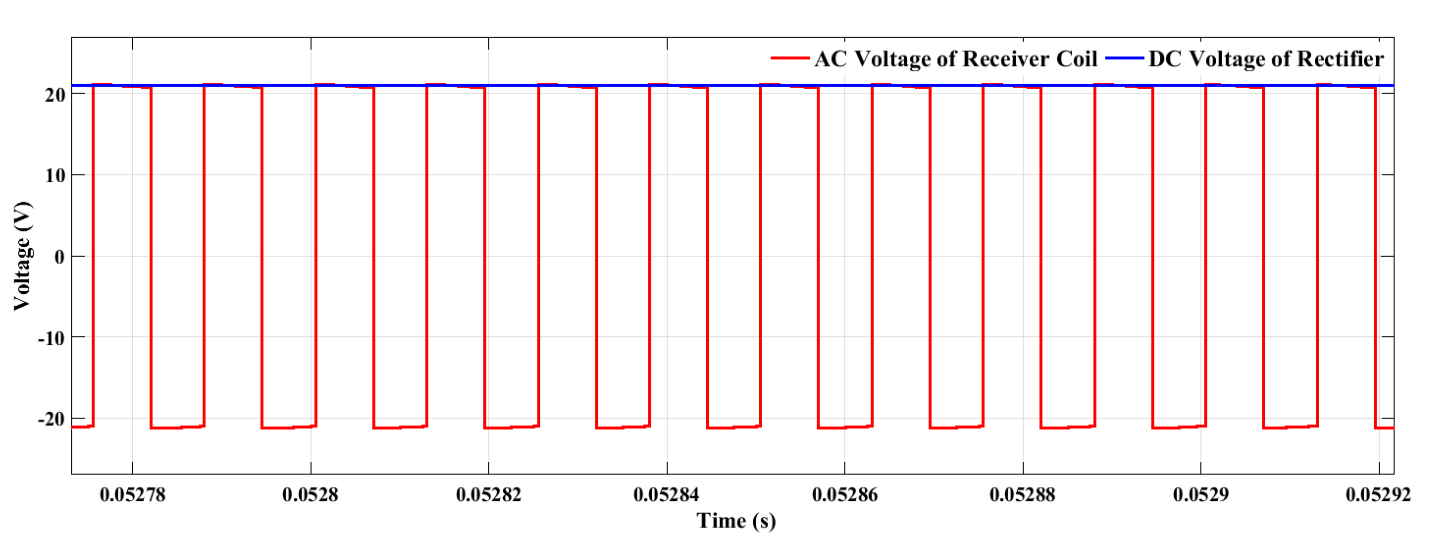
3.3. Charging the EV Battery with Invented GaN Inverter—Experimental Tests and Results

To achieve the last goal of the project, the implemented GaN inverter was tested for lab-scale wireless charging of the EV battery. The whole circuit system was assembled according to Figure 16, and all parts/components in the system were implemented based on the simulated design in Figure 1. While the inverter output results on the transmitter side were thoroughly discussed in the previous subsections, this segment will specifically consider the output waveforms of the receiver side, as well as the charging of the battery.
After receiving AC voltage from the receiver coil, the rectifier converts the VAC (yellow waveform) to VDC for charging the EV battery (blue waveform), as demonstrated in Figure 17. A small dissimilarity between the simulated results (Figure 3) and experimental waveforms (Figure 17) verified that all parts of the WPT systems were validly simulated and constructed in the research laboratory, and able to be adjusted and developed for real-world manufacturing.
The battery applied in the wireless charging system with an initial ~5 V boasts a more reasonable charging time than the original simulation. In the experiment, the 48 V battery was charged in 11.04 min as displayed in Figure 18, while the simulation results indicated 39 min to charge the same battery as demonstrated in Figure 4. This significant discrepancy arises from limitations in the MATLAB Simulink software, as the software lacks enough setting options to input all of the features that the GaN switches have to offer. Hence, the purchased GaN switches out-performed the simulation at high frequencies. Likewise, controlling the half-bridge GaN inverter with Silicon Lab’s gate drivers proved to be more precise than the simulation pattern suggested. Therefore, by implementing the proposed WPT system, a real-world EV battery (~400–800 V) will charge in 1.5–3.0 h, which is an effectual charging time for next-generation, lower-cost, and longer lasting electric vehicle batteries.

4. Conclusions

Currently, charging the batteries of electric vehicles wirelessly can be achieved in a remarkable amount of time by generating high-power efficiency. A high-frequency inverter with optimized snubber circuits is required to boost the power output and increase the transferred power between transmitter and receiver coils in the wireless charging system. All listed objectives from the “contributions” section are reflected respectively with their outcomes:
  • After simulating the invented high-frequency H/full-bridge GaN inverter designed with compatible snubber circuits, power dissipation was reduced by 1.2 mW, as well as leakage inductance, by 90 nH.
  • Following the simulation of wireless power transfer in EVs, the developed GaN inverter was tested, resulting in ~93% efficiency at high switching frequencies (80 kHz). This energy-efficient inverter technology is, therefore, accurate and applicable in the proposed EV circuit system.
  • By comparing the simulated and experimental results of the EV wireless charging system with/without the designed snubber circuits, it was confirmed that RCD snubber circuits and Series-Series compensators are imperative for reducing voltage spikes and harmonic distortions by 11 V, increasing coil efficiency by ~4%, improving inverter output function, and preventing excess current. To achieve these results, the following ranges were optimized: resistor 545–560 Ω and capacitor 150–250 PF.
  • The wireless charging system, along with a single-phase GaN inverter controlled by the Si8231AB gate drivers, was implemented. Results were authenticated by lab-scale experiments of the designed inverter for charging the EV batteries. Consequently, a decrease in the required charging time for 48 V EV batteries was achieved (11.04 min).
The innovative GaN inverter will benefit well-known EV manufacturers, such as Tesla Inc., Chevrolet, BMW®, and Nissan, by boasting significantly lower production costs. Additionally, with respect to the established WPT system, a realistic EV battery (~400–800 V) will reach a full charge in 1.5–3.0 h. This achievement in charging time is operative for next-generation and million-mile electric vehicle batteries. Future projects should focus on simulating and constructing a real-world GaN inverter at Megahertz frequencies, adhering to the approach framed in this article.

Author Contributions

Conceptualization: F.R. and M.B.; Methodology: F.R. and P.N.; Software: F.R. and P.N.; Validation: F.R. and M.B.; Investigation: F.R.; Writing—original draft preparation: F.R.; Writing—review and editing: M.B. and T.A.; Supervision: M.B. All authors have read and agreed to the published version of the manuscript.

Funding

This research received no external funding.

Acknowledgments

Authors acknowledge support from Lamar University’s Center of Midstream Management and Science (CMMS) and Transphorm Inc.

Conflicts of Interest

The authors declare no conflict of interest.

References

  1. Martinez, W.; Odawara, S.; Fujisaki, K. Sampling frequency influence on magnetic characteristic evaluation under high frequency GaN inverter excitation. In Proceedings of the 2017 IEEE 3rd International Future Energy Electronics Conference and ECCE Asia (IFEEC 2017-ECCE Asia), Kaohsiung, Taiwan, 3–7 June 2017. [Google Scholar]
  2. Wang, B.; Monti, A.; Riva, M. A high-speed H-bridge circuit based on GaN HFETs and custom resonant gate drivers. In Proceedings of the 2009 IEEE Energy Conversion Congress and Exposition, San Jose, CA, USA, 20–24 September 2009. [Google Scholar]
  3. Kawai, Y.; Nagai, S.; Tabata, O.; Fujiwara, H.; Negoro, N.; Ueno, H.; Ishida, M.; Otsuka, N. An isolated DC power supply free compact GaN inverter module. In Proceedings of the 2015 IEEE 11th International Conference on Power Electronics and Drive Systems, Sydney, Australia, 9–12 June 2015. [Google Scholar]
  4. Li, H.; Li, X.; Zhang, Z.; Yao, C.; Wang, J. Design consideration of high power GaN inverter. In Proceedings of the 2016 IEEE 4th Workshop on Wide Bandgap Power Devices and Applications (WiPDA), Fayetteville, AR, USA, 7–9 November 2016. [Google Scholar]
  5. Ramachandran, R.; Nymand, M. An energy recovery clamp circuit for an isolated DC-DC GaN converter. In Proceedings of the 2016 IEEE International Telecommunications Energy Conference (INTELEC), Austin, TX, USA, 23–27 October 2016. [Google Scholar]
  6. Jiang, L.; Costinett, D. A high-efficiency GaN-based single-stage 6.78 MHz transmitter for wireless power transfer applications. IEEE Trans. Power Electron. 2018, 34, 7677–7692. [Google Scholar] [CrossRef]
  7. Wu, J.; Li, Y.; Jin, N.; Deng, W.; Tang, H.; Snášel, V. A GaN-based wireless power and information transmission method using Dual-frequency Programmed Harmonic Modulation. IEEE Access 2020, 8, 49848–49856. [Google Scholar] [CrossRef]
  8. Trung, N.K.; Akatsu, K. Design 13.56 MHz 10 kW resonant inverter using GaN HEMT for wireless power transfer systems. In Proceedings of the 2017 IEEE Energy Conversion Congress and Exposition (ECCE), Cincinnati, OH, USA, 1–5 October 2017; pp. 955–960. [Google Scholar]
  9. Agamloh, E.; Jouanne, A.V.; Yokochi, A. An Overview of Electric Machine Trends in Modern Electric Vehicles. Machines 2020, 8, 20. [Google Scholar] [CrossRef] [Green Version]
  10. Seo, D.-W.; Lee, J.-H.; Lee, H.-S. Optimal coupling to achieve maximum output power in a WPT system. IEEE Trans. Power Electron. 2015, 31, 3994–3998. [Google Scholar] [CrossRef]
  11. Zhao, C.; Costinett, D. GaN-based dual-mode wireless power transfer using multifrequency programmed pulse width modulation. IEEE Trans. Ind. Electron. 2017, 64, 9165–9176. [Google Scholar] [CrossRef]
  12. Cai, A.; Pereira, A.; Tanzania, R.; Tan, Y.K.; Siek, L. A high frequency, high efficiency GaN HFET based inductive power transfer system. In Proceedings of the 2015 IEEE Applied Power Electronics Conference and Exposition (APEC), Charlotte, NC, USA, 15–19 March 2015; pp. 3094–3100. [Google Scholar]
  13. Puukko, J.; Xu, J.; Liu, L. Consideration of flyback converter using GaN devices. In Proceedings of the 2015 IEEE 3rd Workshop on Wide Bandgap Power Devices and Applications (WiPDA), Blacksburg, VA, USA, 2–4 November 2015; pp. 196–200. [Google Scholar]
  14. Niknejad, P.; Agarwal, T.; Barzegaran, M. Utilizing Sequential Action Control Method in GaN-Based High-Speed Drive for BLDC Motor. Machines 2017, 5, 28. [Google Scholar] [CrossRef] [Green Version]
  15. De Pinto, S.; Mantriota, G. Power Flows in Compound Transmissions for Hybrid Vehicles. Machines 2019, 7, 19. [Google Scholar] [CrossRef] [Green Version]
  16. Lei, Y.; Barth, C.; Qin, S.; Liu, W.-c.; Moon, I.; Stillwell, A.; Chou, D.; Foulkes, T.; Ye, Z.; Liao, Z. A 2 kW, single-phase, 7-level, GaN inverter with an active energy buffer achieving 216 W/in3 power density and 97.6% peak efficiency. In Proceedings of the 2016 IEEE Applied Power Electronics Conference and Exposition (APEC), Long Beach, CA, USA, 20–24 March 2016; pp. 1512–1519. [Google Scholar]
  17. Morita, T.; Tamura, S.; Anda, Y.; Ishida, M.; Uemoto, Y.; Ueda, T.; Tanaka, T.; Ueda, D. 99.3% efficiency of three-phase inverter for motor drive using GaN-based gate injection transistors. In Proceedings of the 2011 Twenty-Sixth Annual IEEE Applied Power Electronics Conference and Exposition (APEC), Fort Worth, TX, USA, 6–11 March 2011; pp. 481–484. [Google Scholar]
  18. Shirabe, K.; Swamy, M.; Kang, J.-K.; Hisatsune, M.; Wu, Y.; Kebort, D.; Honea, J. Advantages of high frequency PWM in AC motor drive applications. In Proceedings of the 2012 IEEE Energy Conversion Congress and Exposition (ECCE), Raleigh, NC, USA, 15–20 September 2012; pp. 2977–2984. [Google Scholar]
  19. Rahmani, F.; Quispe, D.; Agarwal, T.; Barzegaran, M. Speed control of brushless DC motor by DC-DC boost and buck converters using GaN and SiC transistors for implementing the electric vehicles. Comput. Res. Prog. Appl. Sci. Eng. 2020, 6, 40–45. [Google Scholar]
  20. Blumenfeld, A.; Cervera, A.; Ben-Yaakov, S. Analysis and design of DC-isolated gate drivers. In Proceedings of the 2012 IEEE 27th Convention of Electrical and Electronics Engineers in Israel, Eilat, Israel, 14–17 November 2012; pp. 1–5. [Google Scholar]
  21. SAE International. Wireless Power Transfer for Light-Duty Plug-In/Electric Vehicles and Alignment Methodology; SAE International: Warrendale, PA, USA, 2016. [Google Scholar]
  22. Instruments, T. SAE J1772-Compliant Electric Vehicle Service Equipment Reference Design for Level 1 and 2 EV Charger. Available online: https://www.ti.com/lit/ug/tiduer6/tiduer6.pdf?ts=1598717673960&ref_url=https%253A%252F%252Fwww.google.com%252F (accessed on 1 October 2019).
  23. Todd, P.C. Snubber circuits: Theory, design and application. In Proceedings of the Unitrode-Power Supply Design Seminar, Dallas, TX, USA, 18 January 2001; p. 1993. [Google Scholar]
  24. Traxler, J.C.; Whitham, I.R.C. Switching Power Supply. Google Patents 4,916,599, 10 April 1990. [Google Scholar]
  25. Mohan, N.; Robbins, W.P.; Undeland, T. Power electronics: Converters, applications and design. Microelectron. J. 2003. [Google Scholar] [CrossRef]
  26. Vázquez, J.; Roncero-Sánchez, P.; Parreño Torres, A. Simulation model of a 2-kW IPT charger with phase-shift control: Validation through the tuning of the coupling factor. Electronics 2018, 7, 255. [Google Scholar] [CrossRef] [Green Version]
  27. Posthuma, N.; You, S.; Stoffels, S.; Wellekens, D.; Liang, H.; Zhao, M.; De Jaeger, B.; Geens, K.; Ronchi, N.; Decoutere, S. An industry-ready 200 mm p-GaN E-mode GaN-on-Si power technology. In Proceedings of the 2018 IEEE 30th International Symposium on Power Semiconductor Devices and ICs (ISPSD), Chicago, IL, USA, 13–17 May 2018; pp. 284–287. [Google Scholar]
Figure 1. Wireless charging circuit contains: (a) AC voltage source, transmitter rectifier, GaN inverter with gate drivers, and transmitter coil; (b) Receiver coil, receiver rectifier, and battery.
Machines 08 00056 g001aMachines 08 00056 g001b
Figure 2. Simulation results of power supply, transmitter rectifier, and GaN inverter.
Machines 08 00056 g002
Figure 3. Simulated voltage output of receiver coil and rectifier.
Machines 08 00056 g003
Figure 4. Simulation of electric vehicle battery charging in 10 s.
Machines 08 00056 g004
Figure 5. The snubber capacitance and resistance optimization based on the inverter efficiency.
Machines 08 00056 g005
Figure 6. Checking the maximum efficiency of different elements in the WPT system to verify the optimized snubber resistance.
Machines 08 00056 g006
Figure 7. Improving the output waveform of the GaN inverter using corresponding snubber circuits.
Machines 08 00056 g007
Figure 8. Simulated and experimental design of SI8231AB-D-IS gate driver to control GaN half-bridge inverter.
Machines 08 00056 g008
Figure 9. Yellow signals: Gate driver input signal, Blue signals: (a) High-level voltage of gate driver output in ON mode, controlling the top transistor of the half-bridge inverter; (b) low-level voltage of gate driver output in OFF mode, controlling the bottom transistor of the half-bridge inverter.
Machines 08 00056 g009
Figure 10. Prototype of GaN inverter without snubber circuits; 1: GaN inverter, 2: 1st gate driver, 3: 2nd gate driver, 4: Sending signals to the gate drivers, 5: 5 VDC of the gate drivers, 6: 9.1 VDC of the gate drivers, 7: Input VDC of GaN inverter.
Machines 08 00056 g010
Figure 11. Output VAC and input VDC of full-bridge GaN inverter without snubber circuits; Excel spreadsheet is extracted from Analog Discovery.
Machines 08 00056 g011
Figure 12. Testing the half-bridge GaN inverter with RCD snubber circuits; 1: Half-bridge inverter, 2: Gate Driver, 3: Load.
Machines 08 00056 g012
Figure 13. (a) 1st and (b) 2nd half-bridge outputs of GaN inverters, controlled by their respective gate drivers.
Machines 08 00056 g013
Figure 14. Prototype of GaN inverter including RCD snubber circuit; 1: Full-bridge GaN inverter, 2: 1st gate driver, 3: 2nd gate drive, 4: Sending signals to the gate drivers.
Machines 08 00056 g014
Figure 15. Output VAC and input VDC of full-bridge GaN inverter with snubber circuits; Excel spreadsheet is extracted from Analog Discovery.
Machines 08 00056 g015
Figure 16. Lab-scale prototype of dynamic wireless charging for EV battery; 1: AC Power Supply, 2: Transmitter Rectifier, 3: GaN Inverter with its gate drivers, 4: Transmitter Coil, 5: Receiver Coil, 6: Receiver Rectifier, and 7: Batteries.
Machines 08 00056 g016
Figure 17. Receiver coil and rectifier output waveforms to charge the EV battery.
Machines 08 00056 g017
Figure 18. Experimental charging of electric vehicle battery in 90 s; Excel spreadsheet is extracted from Analog Discovery.
Machines 08 00056 g018
Table 1. Characteristics of WPT system components.
Transmitter Side of WPT SystemReceiver Side of WPT System
Transmitter Rectifier Resistances100 kΩReciever Rectifier Resistances10 kΩ
Transmitter Rectifier Capacitances100 μFReciever Rectifier Capacitances0.1 μF
Input Capacitance (CI)100 μFInput Capacitance (CL)100 μF
Transmitter compensator (Ct)190 nFReciever compensator (Cr)190 nF
Power Supply30 VBattery Size336 W/48 V
Transmitter Inductance36.01 μHReciever Inductance34.81 μH
Transformer Turns Ratio1:1Transformer CoilCopper 0.99
Number of Turns (N)10Transformer CoreFerrite 1000
Mutual Inductance (M)21.99 μHPermeability of Air (μo) 1 H/m
Total Air Gap148.36 mmCoil Length (LW)7.9 m
Switching Frequency80 kHzBreadth of Winding (BW)35 mm

