
Review

Multispectral Sensor Fusion and YOLO-Family Benchmarking in PCB Component Detection: Challenges, State of the Art, and Future Directions

1
The Graduate Center, City University of New York, New York, NY 10016, USA
2
Computer Science Department, Graduate Center, College of Staten Island (CSI), City University of New York, New York, NY 10314, USA
*
Author to whom correspondence should be addressed.
Machines 2026, 14(7), 730; https://doi.org/10.3390/machines14070730
Submission received: 22 May 2026 / Revised: 21 June 2026 / Accepted: 23 June 2026 / Published: 28 June 2026
(This article belongs to the Special Issue Design and Manufacturing for Lightweight Components and Structures)

Abstract

The worldwide spread of semiconductor devices has driven a surge in electronic waste (e-waste), which reached 62 million metric tons in 2022 and is projected to exceed 80 million metric tons by 2030. E-waste contains hazardous substances such as cadmium and mercury, yet also represents a $57 billion annual opportunity through the recovery of valuable and critical raw materials (CRMs). However, formal recycling rates remain stagnant at 22.3%, largely due to limitations of current automated sorting methods. These systems primarily rely on visible-light (RGB) imaging, which lacks the spectral resolution needed to distinguish chemically similar polymers, complex metal alloys, and composite substrates on printed circuit boards (PCBs). This paper presents a multidisciplinary synthesis of AI-driven detection and classification for e-waste, bridging materials science and computer vision through three interconnected themes. 1. Material and Economic Context: The toxicological risks and economic drivers of semiconductor recycling are characterized, framing fine-grained material identification as essential for a circular economy. 2. Multispectral Sensing & Fusion: Sensing modalities such as near-infrared (NIR), hyperspectral imaging (HSI), and X-ray fluorescence (XRF) are assessed, and sensor fusion strategies, including early, late, and intermediate fusion, are reviewed for high-throughput industrial settings. 3. Deep Learning Benchmarking: 11 publicly available PCB datasets are analyzed, and the YOLO series (YOLOv3–YOLOv12) is compared with leading non-YOLO detectors, including Faster R-CNN, RT-DETR-L, and RetinaNet. The results show that while YOLOv9s achieves a peak mAP@0.5 of 56.5% and YOLOv11s offers an optimal industrial profile (37.2% mAP@0.5:0.95 at 115 ms edge inference), all RGB-based models fail to detect visually ambiguous surface-mount devices (SMDs), with mAP values below 12%. This confirms a performance ceiling for purely visual systems. The review concludes that transitioning from RGB-centric to multispectral fusion architectures is the primary research frontier and proposes a roadmap for standardized multimodal datasets and edge-deployable fusion models to enable next-generation, high-recovery automated recycling.

1. Introduction

Semiconductors underpin almost all modern technologies—from smartphones and electric vehicles to medical and aerospace systems. However, this progress comes with a high environmental cost: e-waste is now one of the fastest-growing waste streams worldwide [1]. E-waste includes discarded devices powered by batteries or electricity, such as laptops, mobile phones, lab instruments, and their components [2]. Many devices are discarded well before reaching the end of their useful lives, driven by declining electronics costs, rapid product cycles, and consumer upgrade habits [3,4]. The issue is multidisciplinary, affecting technology supply chains, waste management, human health, policy, and global environmental sustainability [5].
In 2022, the world produced 62 million tons of e-waste [1], enough to encircle the Earth if loaded onto 40-ton trucks, yet only 22.3% was officially recycled [6]. Recycling rates specific to semiconductors are even lower, well below the global average of 17.4% [7]. Urgency is driven by three factors:
  • E-waste toxicity: e-waste contains arsenic, lead, cadmium, and gallium arsenide, which contaminate soil and water when mishandled [8,9]. Children and pregnant women are especially at risk; an estimated 16.5 million children worked in waste-processing sectors in 2020 [6].
  • Resource loss: e-waste contains about $57 billion in recoverable materials each year—such as gold, silver, copper, palladium, and rare earth elements—but less than $10 billion is actually recovered [10,11].
  • Materials scarcity: efficient recovery—driven by critical minerals with unreliable supply chains—is a key economic and geopolitical concern.
Despite these stakes, traditional recycling methods rely on labor-intensive manual sorting, low-precision mechanical separation, and informal recycling practices, leading to low recovery rates, worker health risks, and environmental contamination [12]. PCBs pose particular challenges: their multi-material, microscale composition makes accurate identification nearly impossible using RGB imaging alone, especially when components are overlapped, degraded, or contaminated. Although substantial research has addressed general e-waste management, three core gaps persist in semiconductor-specific recycling.

1.1. Limitations of Current AI-Based Approaches

Gap 1: Laboratory-only PCB component detection. Most studies on PCB component detection focus on manufacturing quality control under controlled conditions with pristine boards [13,14,15]. While accuracies often exceed 95%, these models degrade in real recycling facilities, where lighting variability, dust, corrosion, and broken components dramatically reduce performance—especially for small surface-mount devices (SMDs), ICs, and polymer types.
Gap 2: Overreliance on RGB imaging. Current AI-based waste classifiers rely heavily on visible RGB images [16,17,18], which cannot distinguish visually similar materials. PCB substrates, plastics (ABS, PVC, PC), and metal alloys often appear indistinguishable under visible light. Advanced sensing, including hyperspectral imaging (HSI), near-infrared (NIR) spectroscopy, and thermal imaging, enables material-level differentiation [19]. Yet no field-ready framework integrates these modalities into real-time sorting systems capable of fusing spatial, spectral, and thermal signatures.
Gap 3: Lack of closed-loop automation and small datasets. Most systems function only as isolated detectors, without connection to robotic actuators or adaptive sorting controls. Variability in component streams cannot be compensated for in real time. A further barrier is the scarcity of labeled PCB datasets: annotating hundreds of fine-grained device types is expensive and highly specialized, restricting robust deep learning model training.

1.2. Scope and Contributions of This Review

Prior reviews of AI in e-waste focus on high-level trends rather than semiconductor-specific waste streams:
  • Circular Economy frameworks: Bressanelli et al. [20] and Goyal & Gupta [21] analyze lifecycle strategies across the WEEE ecosystem, but do not address material-level AI classification.
  • Traditional recycling processes: Wu et al. [22] examine disassembly, pyrolysis, hydrometallurgy, and bioleaching for metals recovery but overlook intelligent sorting automation.
  • Recovery-rate prediction: Choubey et al. [23] use AI to estimate recovery efficiencies, but do not tackle component-level PCB recognition.
  • Manufacturing defect detection: Roy et al. [24], Ghelani [25], and Alyammahi [26] focus on quality control, not waste variability.
  • Selective disassembly: Mohsin et al. [27] highlight the use of deep learning to locate high-value PCB components, but note the absence of integrated robotic, spectral, or economic decision-making tools.
To address these challenges, this review provides the first comprehensive synthesis across three tightly connected domains:
(i)
AI-driven PCB detection and fine-grained recognition (Section 5): covering CNNs, transformers, hierarchical models, small-object detection, and the full YOLO family for contaminated waste environments.
(ii)
Multispectral material classification (Section 3): evaluating fusion of RGB, HSI, NIR, and XRF data to distinguish polymers, metals, and substrate materials with high spectral sensitivity.
(iii)
Systematic benchmark and real-time sorting (Section 6): seven YOLO variants and three non-YOLO detectors (Faster R-CNN, RT-DETR-L, and RetinaNet) are evaluated on a common PCB dataset, hardware, and training protocol. All detectors are used in their unmodified, published form, so that performance differences can be attributed to the architectural family itself rather than to model-specific tuning. The results are interpreted architecturally and linked to actuator control and value estimation for automated recycling lines.
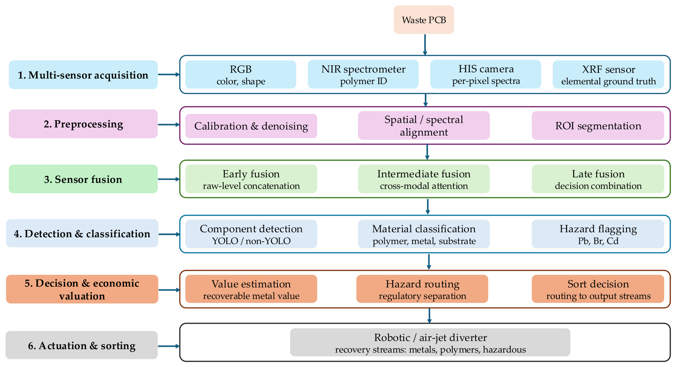
Unlike prior reviews, this work targets semiconductor-specific waste streams, addresses deployment constraints, and emphasizes industrial readiness in terms of speed, robustness, and cost. The aim is not to propose a new detector but to map how existing architectures behave under realistic PCB-recycling conditions and to identify multispectral fusion as the most promising direction for future architectural work. Figure 1 illustrates the end-to-end conceptual framework that organizes the remainder of the paper.

2. E-Waste Composition, Toxicity, and Metal Value

PCBs are simultaneously the most economically valuable and the most hazardous component of the e-waste stream. Their heterogeneous mixture of precious metals, toxic heavy metals, and halogenated polymers creates a fundamental tension: the same board that contains recoverable gold also harbors lead, cadmium, and brominated flame retardants. This section surveys the material composition of PCBs (Section 2.1), their hazardous constituents and health consequences (Section 2.2), and the three established metallurgical pathways for metal recovery—along with the case for why intelligent upstream sorting improves all three (Section 2.3).

2.1. Material Composition of E-Waste and PCBs

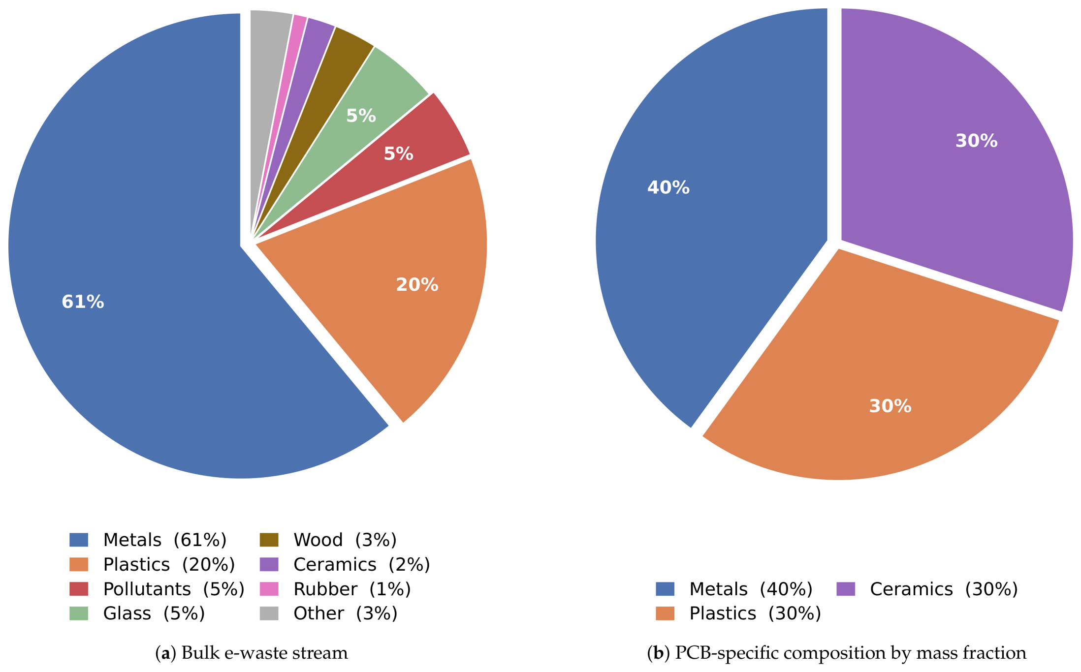
A typical e-waste stream contains up to 69 distinct metals, with bulk fractions distributed as metals 61%, plastics 20%, glass 5%, ceramics 2%, and residual pollutants 5% [10]. Although PCBs represent only 3–7% of total e-waste by mass, they are its most economically valuable component [10,28]. A discarded PCB (DPCB) consists of three main elements: a polymer-resin substrate reinforced with glass-fiber and laminated copper foil, tin-based solder alloys, and a population of surface-mounted and through-hole electronic components [28]. At the macroscopic level, DPCBs contain a metal fraction of 30–50% and a non-metal fraction of 50–70% by weight, with ratios varying substantially by device type (Table 1). Figure 2 shows the bulk and PCB-specific mass fractions.
High-grade boards from smartphones and CPUs additionally carry precious metals: gold (250–2050 ppm), silver (110–4500 ppm), and palladium (40–4000 ppm) [10]—concentrations 50 times higher in Au and 26 times higher in Cu than equivalent masses of primary ore [28]. Wu et al. [22] showed that electronic components (ICs, capacitors, connectors) account for approximately 77% of the total metal weight of a DPCB, with each component type carrying a characteristic metal signature: MLCCs concentrate barium, palladium, and gold; tantalum capacitors concentrate tantalum; and ICs are the principal reservoir of copper and gold wire-bonds. Coarse mechanical shredding destroys this spatial segregation, simultaneously diluting precious-metal concentrations and releasing toxic substances into process media [22,28]. Intelligent component-level detection before metallurgical treatment is, therefore, a necessary condition for maximizing recovery yield.

2.2. Hazardous Substances and Health Consequences

Semiconductor manufacturing involves hazardous materials, including arsenic, gallium, lead, and doping chemicals, which are embedded in complex component matrices, making their extraction and disposal challenging [30,31]. Gallium arsenide (GaAs), used in high-frequency chips, is highly toxic and requires specialized recycling. Arsenic causes breathing and liver disease as well as bladder cancer [8]. Research by Chalana et al. [9] found high levels of Ni (0.4%), Pb (1.5%), Zn (2.1%), Ba (0.3%), and Cd (310 mg/kg) in soil at CRT storage sites, with lead concentrations 50 times above background levels (1580 vs. 30 mg/kg). When PCBs are processed through informal recycling, such as open burning or uncontrolled acid leaching, these substances are released into soil, water, and air in persistent, bioaccumulative forms [28,32]. Children and pregnant women are especially vulnerable, as lead, mercury, and cadmium cross the placental barrier and accumulate in developing neural tissue [6,9]. Table 2 summarizes the principal toxic substances and their health consequences.
An important observation for this review is that many of the most hazardous substances listed in Table 2 are visually indistinguishable from their benign counterparts under conventional RGB cameras: lead-based solder (Sn–Pb) and lead-free solder (Sn–Ag–Cu) are nearly identical in color and surface reflectance; polyvinyl chloride (PVC) and acrylonitrile butadiene styrene (ABS) share the same visible-light appearance despite dramatically different combustion chemistry; and brominated and non-brominated FR4 laminates are visually indistinguishable [38,39]. This spectral blindness of RGB imaging is not merely an inconvenience; it is a structural limitation that prevents AI-based sorting systems operating on visible-light data alone from identifying and segregating hazardous materials before downstream processing. The multispectral sensing modalities reviewed in Section 3 directly address this gap.

2.3. Economic Value and Metal Recovery Pathways

The recoverable raw-material value of global e-waste is approximately $57 billion annually [10,28], yet less than $10 billion is reclaimed through formal recycling [1]. This disparity results from upstream inefficiencies, heterogeneous feedstock, insufficient sorting, and contamination by co-mingled hazardous materials, rather than limitations in metallurgical technology [22]. As shown in Table 3, the 2019 global e-waste stream contained an estimated 1808 kt of copper, 0.2 kt of gold, and 0.1 kt of palladium, with a combined recoverable value exceeding $48 billion [10]. These figures establish discarded electronics as one of the richest urban mining resources.
Three principal metallurgical pathways recover metals from waste PCBs, and all three benefit directly from improved upstream sorting.
Pyrometallurgy uses high-temperature smelting or pyrolysis to separate metals from non-metallic matrices and is the most industrially mature route [10]. The Umicore smelter in Hoboken, Belgium, processes 350,000 tons of e-waste annually, recovering over 100 tons of gold and 2400 tons of silver per year [10]. Its key limitation is that plastics cannot be recovered, and brominated materials generate toxic dioxin emissions (PCDD/PCDF) during combustion, making pre-removal of halogenated laminates a direct operational requirement [22,32].
Hydrometallurgy dissolves target metals into aqueous solution using acids, cyanide, or thiosulfate lixiviants, followed by electrowinning or solvent extraction for high-purity recovery [10,22]. It offers better metal selectivity and lower infrastructure cost than pyrometallurgy, but halogenated organics inhibit leaching efficiency and poison catalyst surfaces [22]. NIR spectroscopy and HSI can identify brominated polymers in real time, providing exactly the upstream intelligence hydrometallurgical plants need (Section 3).
Biohydrometallurgy uses acidophilic bacteria, such as Acidithiobacillus ferrooxidans, to solubilize metals at ambient temperature and pressure, thereby avoiding toxic reagents and producing minimal secondary waste [32,40]. It is the most environmentally attractive route but the slowest (days to weeks), and microbial activity is strongly inhibited by heavy metals and halogenated compounds, requiring clean, sorted feedstock to achieve viable leaching rates [10].
The three pathways described above are not mutually exclusive. Industrial practice increasingly integrates them in hybrid sequences (mechanical pre-treatment, pyrometallurgy, hydrometallurgical refining of recovered metals) [22,41]. All three approaches share a critical dependence on feedstock quality: the purity, metal concentration, and absence of inhibitory contaminants in the input material directly determine process efficiency and ultimate recovery yield.
Oke and Potgieter [28] and Wu et al. [22] both emphasize that disassembly and sorting are the first and most impactful steps in the recycling chain. Mohsin et al. [27] showed that deep-learning-based component detection can locate and classify high-value electronic components on waste PCBs with near 99% precision under controlled conditions. Lu et al. [42] demonstrated an automated sorting system for detached components that achieved industrial throughput. As demand for copper is projected to increase by 275–300% by 2050, a level unlikely to be met through virgin mining alone [10], economic incentives to recover every possible gram from secondary sources are expected to intensify. This establishes the central motivation for this review: AI-driven multispectral component detection is not an academic exercise but a necessary step toward closing the ∼US $47 billion annual gap between the recoverable and recovered value of the global e-waste stream.

3. Multispectral and Hyperspectral Imaging for Material Identification

As established in Section 2, many of the most hazardous and valuable materials in waste PCBs are visually indistinguishable under conventional RGB imaging. Leaded and lead-free solders share similar surface reflectance; brominated and non-brominated laminates cannot be separated by color alone; and copper, tin, and nickel plating appear nearly identical in visible light [38,39]. These limitations are not incidental deficiencies of individual systems but structural constraints of the visible spectrum: the 380–700 nm window simply does not carry the molecular and elemental information needed for reliable material discrimination in a heterogeneous waste stream.
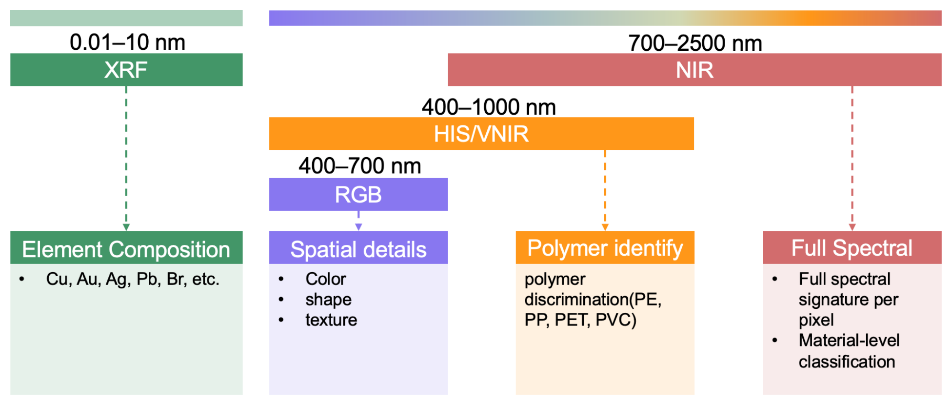
This section reviews four sensing modalities that extend beyond visible light and that are relevant to PCB recycling: RGB imaging (Section 3.1), near-infrared spectroscopy and hyperspectral imaging (Section 3.2), and X-ray fluorescence (Section 3.3). Each modality is characterized by its operating wavelength range, physical principle, detection capability, and practical limitations. Section 3.4 then examines strategies for combining multiple modalities to overcome the limitations of individual sensors. Table 4 and Figure 3 present a consolidated comparison.

3.1. RGB

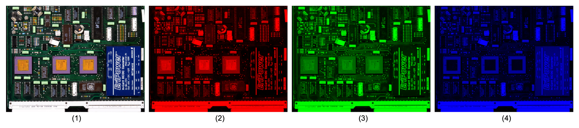
Color representation in digital imaging uses the RGB color space model, where the color of a pixel consists of three channels: red (R), green (G), and blue (B). It is possible to reproduce all colors by combining various intensities of the three channels. Figure 4 shows the original PCB image and images of the three channels in the RGB color space.
While RGB is the standard, most intuitive way to map colors on a PCB, it has a major weakness: it is highly sensitive to changes in lighting and environment. Because the Red, Green, and Blue channels are deeply intertwined, changing just one channel shifts the overall brightness and alters how the other two are perceived. This high correlation means that even a tiny fluctuation in light intensity can make two entirely different components look identical. This becomes a real headache when a system is trying to distinguish between similarly colored parts, such as surface-mount resistors and inductors [47].

3.2. NIR and Hyperspectral Sensing

The main limitation of visual object sorting using RGB cameras is the requirement for controlled lighting and a limited workspace. To overcome this obstacle and classify recyclables, thermographic and spectral imaging approaches are used [48]. Near-infrared (NIR) spectroscopy (wavelength range 700–2500 nm) and hyperspectral imaging (HSI, capturing 100–200+ spectral bands) provide material-specific signatures based on molecular vibrations and electronic transitions [38,39].
In polymer sorting, NIR has demonstrated greater than 95% accuracy for distinguishing polyethylene (PE), polypropylene (PP), polyethylene terephthalate (PET), and polyvinyl chloride (PVC) [39]. For e-waste specifically, Picón et al. [46] combined hyperspectral imaging (400–1000 nm) with CNNs, achieving approximately 23% improvement in classification accuracy over RGB-only methods for PCB component identification, from approximately 74% with RGB alone to approximately 97% with HSI, confirming the critical value of spectral information for fine-grained component discrimination.
Recent work continues to confirm this advantage: Hussein et al. [49] applied a deep learning model to hyperspectral images of e-waste using only three selected spectral bands and reported a 23% accuracy gain over an RGB-only baseline, underscoring that even a small number of well-chosen spectral bands carries material information unavailable in the visible range. Similarly, Moroni et al. [50] used hyperspectral sensing with machine learning to sort plastic waste into individual polymer types, demonstrating the polymer-level discrimination that visible imaging cannot provide and that is directly relevant to separating the polymer fractions of waste PCBs.

3.3. X-Ray Fluorescence (XRF) for Ground Truth Validation

X-ray fluorescence (XRF) is a fast, non-destructive, and versatile technique used to identify the elemental composition of materials from sodium (Na) to uranium (U). The method works by exposing a sample to X-rays, which prompts the material to emit characteristic secondary (fluorescent) X-rays that serve as a fingerprint for each element, enabling both qualitative and quantitative analysis [43]. Key operational advantages include non-destructive testing with the sample remaining intact, near-instant field results without complex chemical preparation, and the ability to detect and quantify elements in solids, liquids, and powders from ppm up to 100% concentration.
In e-waste research, portable XRF has been used to analyze the bromine content of plastic scraps [38], but its use as a ground-truth labeling tool for training supervised deep learning models remains largely unexplored. Beyond brominated flame retardant detection, XRF has proven valuable for comprehensive PCB characterization: Ichikawa et al. [44] employed wavelength-dispersive XRF with a standardless fundamental parameter method to quantify major elements (Al, Si, Ca, Fe, Ni, Cu, Br, Sn, Ba, and Pb) across different particle-size fractions of cryo-milled PCBs, revealing that Cu concentration increased from 2.3% to 45% with particle size, achieving 86.6% Cu recovery from fractions > 250 μm. Similarly, Ferreira et al. [45] combined energy-dispersive XRF with LIBS and multivariate calibration methods (PLS, PCR, MLPCR, ECPR) for quantifying Al, Cu, and Fe in e-waste, achieving limits of detection ranging from 0.001–0.2% w/w and relative errors of 2–33% for Cu and Fe, demonstrating XRF’s capability for both rapid elemental screening and accurate quantification to support automated sorting systems. However, data fusion between LIBS and ED-XRF provided only marginal improvements (3–16%) over single-technique approaches.
The principal limitations of XRF relevant to sorting system design are its surface-only analysis depth (a few micrometers to millimeters), inability to distinguish between different chemical compounds of the same element (e.g., organic vs. inorganic lead), no molecular or isotopic data, sensitivity to sample heterogeneity, and limited detection of light elements (Z < 11). These characteristics mean XRF is best positioned as a complementary modality for elemental ground-truth validation and sorting of metal-rich fractions, rather than as a standalone real-time classifier.

3.4. Sensor Fusion Strategies

Multimodal fusion has emerged as a cornerstone of modern machine learning, enabling systems to integrate information from heterogeneous data sources. Three primary fusion architectures have been established: Early fusion (concatenating raw multispectral inputs before feature extraction), late fusion (combining predictions from separate single-modality networks), and intermediate fusion (merging mid-level features) [51]. Recent advances in transformer-based architectures have further revolutionized this field, with models like CLIP [52,53] and Flamingo demonstrating remarkable cross-modal understanding capabilities. Liang et al. [54] provides a comprehensive analysis of emerging trends, highlighting that the choice of fusion strategy critically impacts model performance, with intermediate fusion often achieving superior results in vision-language tasks by balancing early feature integration with modality-specific representations.
However, multispectral fusion for e-waste classification remains significantly underexplored, with no published research systematically comparing fusion strategies for RGB-NIR e-waste sorting under industrial constraints (inference latency, edge hardware limitations). The critical gap is the absence of optimized fusion architectures that balance classification accuracy, inference speed, and computational efficiency for real-time industrial deployment.
From an industrial-deployment standpoint, the three strategies present distinct trade-offs on a PCB recycling line, where dismantled fractions are carried past an inline imaging stage on a moving conveyor belt and sorted by a robotic manipulator [48]. Late fusion runs an independent network per modality and combines only the final predictions [51]. It is the most deployment-friendly option because it is modular, tolerant of frame-level sensor desynchronization, and easily distributed across edge accelerators. Its drawback is that it discards cross-modal correlations, thereby limiting accuracy for visually ambiguous surface-mount devices [19]. Intermediate fusion merges mid-level features through cross-modal attention and yields the highest accuracy [54]. However, it carries the heaviest computational overhead and the most demanding requirements, namely pixel-level co-registration and sub-frame synchronization between the RGB and NIR/HSI streams. Both are difficult to maintain under mechanical vibration and variable conveyor illumination [38,39]. Early fusion concatenates raw multispectral inputs before feature extraction. Once the inputs are fused, it adds little inference overhead, but it is the most fragile to spatial and spectral misalignment of heterogeneous sensors and to illumination drift. For real-time, vibration-prone, and edge-constrained sorting, late fusion or a lightweight intermediate fusion is the most practicable choice, whereas full intermediate fusion is better suited to slower, controlled inspection stations [13]. Table 5 summarizes these trade-offs.

4. Database

This section reviews the publicly available datasets relevant to PCB component detection and e-waste recycling. Table 6 summarizes and compares them by board count, data volume, modality, inspected components, sensor type, and open-source availability; each dataset is then described in turn below.

4.1. V-PCB

The dataset was acquired using an Arducam 12.4 MP camera, which is connected to an NVIDIA Jetson Nano under diverse recycling conditions. Images were captured with variations in lighting, orientation, camera distance, cast shadows, viewpoints, and resolution. The dataset consists of high-resolution images of waste printed circuit boards (WPCBs), with all images annotated with labeled components such as capacitors, integrated circuits (ICs), electrolytic capacitors, resistors, diodes, transistors, coils, and transformers.
Mohsin et al. [13] utilized this dataset with multiple variants of YOLO models (v8, v9, v10, v11), achieving an impressive average precision of 99.8% and F1-score of 99.5%. It is also observed to have better detection performance with YOLOv11 on high-resolution images ( 1920 × 1920 ).

4.2. PCB-Defect

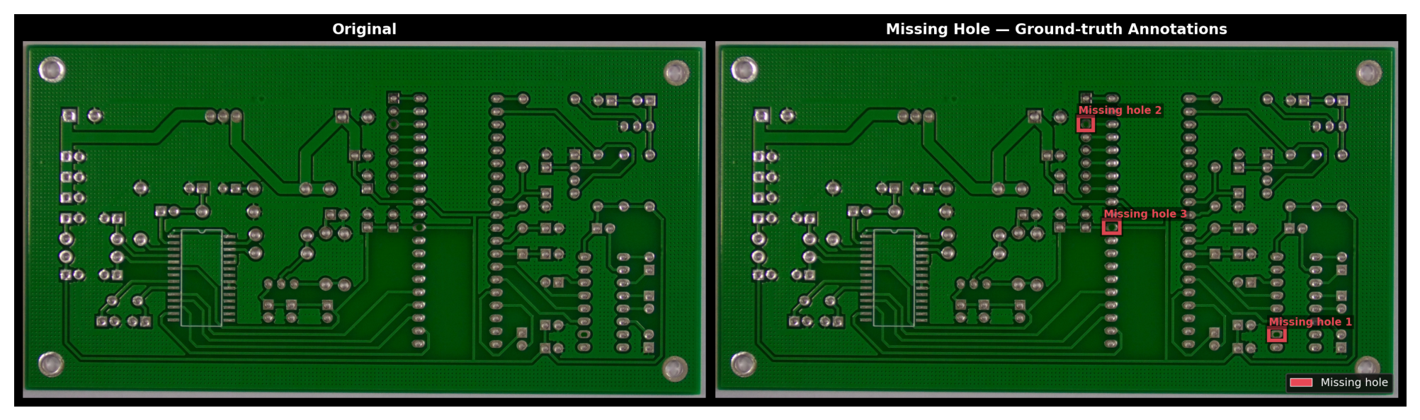
The PCBA-Defect dataset was custom-created by capturing high-resolution images (4608 × 3456 pixels) of PCB template boards using a 16-megapixel industrial camera equipped with adjustable zoom lenses and optimized LED lighting to reduce distortions and shadows [55]. The images are annotated with labels of six defect types, such as missing hole, mouse bite, open circuit, short circuit, spur, and spurious copper, which were manually introduced using Photoshop. Each defect is annotated with bounding boxes and its coordinates pointing to the defect location. Figure 5 shows a sample image along with ground-truth bounding boxes for three missing hole defects. To simulate real-world conditions and support algorithm evaluation for inspection processes, the images were captured in various orientations to improve defect detection performance.

4.3. PCB-Vision

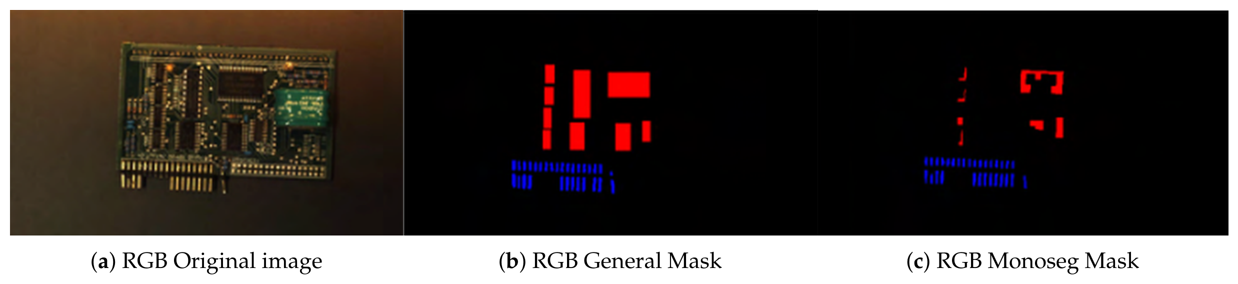
The PCB-Vision dataset includes 53 Printed Circuit Boards (PCBs) captured in RGB format on a conveyor belt using a Teledyne Dalsa C4020 camera, and hyperspectral images (HSI) captured using a Specim FX10 spectrometer. The HSI data spans 224 bands within the VNIR range (400–1000 nm) [19]. Masks are provided for segmentation tasks with the following classes: Others (0), IC (1), Capacitors (2), and Connectors (3). However, these classes are not balanced—object-wise and pixel-wise—across the dataset. These masks are available in both ‘General’ and ‘Monoseg’ formats for segmentation analysis. Figure 6c shows a sample image with the General mask and Monoseg mask.
Arbash et al. [19] achieved a high precision (0.97/0.98) with U-Net and Attention U-Net on a small PCB-Vision dataset (53 images), utilizing RGB-HSI processing despite its challenges.

4.4. PCB-Metal

The PCB-Metal dataset consists of high-resolution PCB images captured with a Canon EOS 5D Mark II DSLR camera under professional lighting conditions, ensuring consistent image quality. It includes bounding box annotations for 5844 IC chips, 3175 capacitors, 2679 resistors, and 542 inductors across 123 PCB boards at varying rotations of 0°, 90°, 180°, and 270° [59]. These annotations help automated systems for component detection and reverse engineering processes that are traditionally manual. Additionally, baseline evaluations of deep learning-based object detection techniques are also included to demonstrate their effectiveness in detecting the IC chips.

4.5. PCB-DSLR

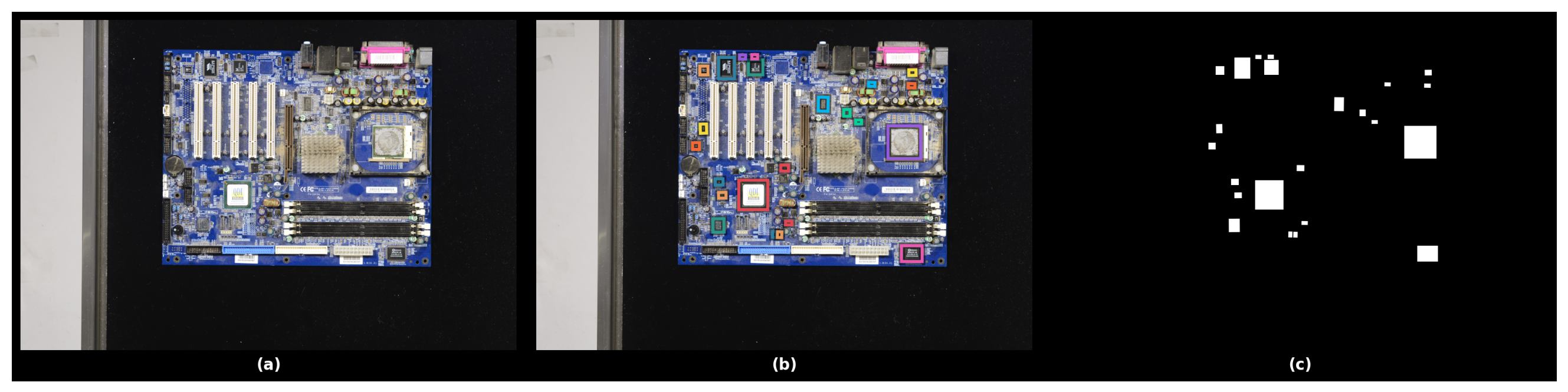
The PCB-DSLR dataset provides high-resolution images (4928 × 3280 pixels at 222 ppi) of 165 PCBs captured using a Nikon D4 DSLR camera with a 60 mm f/2.8 lens mounted above a black conveyor belt to simulate real-world recycling conditions [58]. Also, under conditions with controlled illumination with polarized light, opaque curtains minimize reflections. Each PCB is represented by 3–5 images taken from varying orientations and positions, resulting in the precise detection of components under varying angles, as there are plenty of PCB layers organized differently. The dataset includes segmentation information, bounding box annotations for 9313 IC chips, and textual data for 1740 chips supporting applications such as automatic segmentation, component detection, and text recognition in recycling processes. Figure 7 shows an example of the ground-truth annotations from the dataset.

4.6. FPIC Component

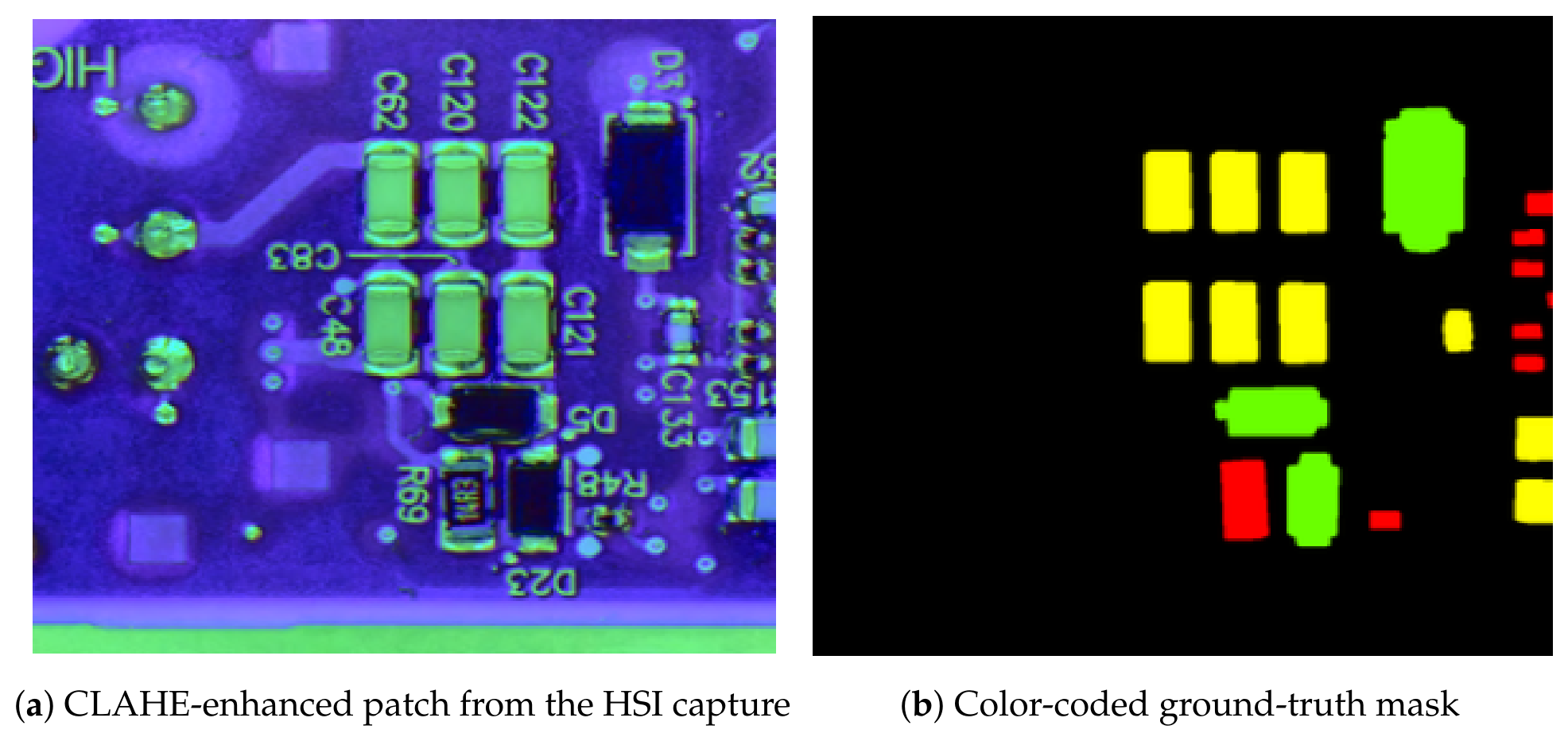
The FPIC Component dataset [63] is derived from high-resolution PCB images captured with a Nikon D850 DSLR across multiple settings. The original dataset contains 93 PCB images with resolutions ranging from 2266 × 1832 to 8291 × 6929 pixels [63]. Considering the computational capabilities, the FPIC-Component subset was focused on images cropped into patches of 768 × 768 pixels on individual components. The images in the dataset are also enhanced using HSI + CLAHE (Contrast Limited Adaptive Histogram Equalization). Figure 8 presents the original patch image along with the mask image for the sample.
This dataset is designed for instance segmentation, semantic segmentation, and object detection tasks relevant to the waste recycling industry. It features 6260 images containing 29,639 labeled objects distributed across 25 classes, such as Resistor (R), Capacitor (C), Integrated Circuit (U), Connector (J), Discrete Transistor (Q), Plug (P), Diode (D), Integrated Circuit (IC), and more. The dataset also provides pixel-level instance segmentation annotations alongside training (5008 images) and validation splits (1252 images).

4.7. WACV PCB Dataset

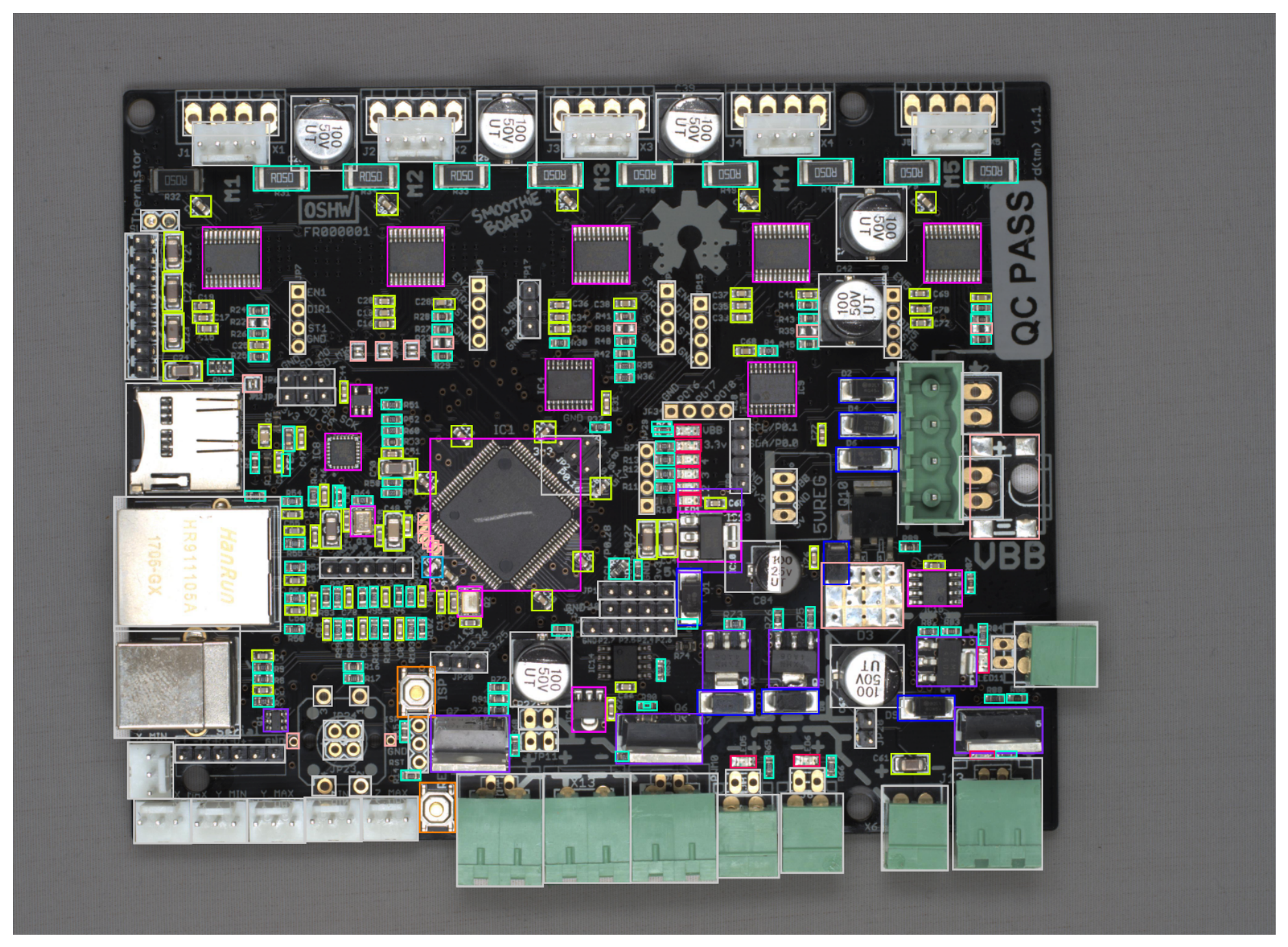
The WACV PCB dataset contains 47 high-resolution images and approximately 62,000 labeled component instances across 31 distinct types [60]. A large proportion of the components are resistors, capacitors, and connectors, resulting in a skewed distribution across classes. It also contains Pixel-level annotations for instance segmentation tasks aimed at detecting individual PCB components. The images following high-resolution imaging standards (15 megapixels or more) were given alongside dense annotations (500 components per PCB). The dataset aims to address challenges such as high intra-class variance and low inter-class variance while supporting automated PCB component analysis. Figure 9 displays two sample images with bounding boxes by component classes.

4.8. Deep PCB

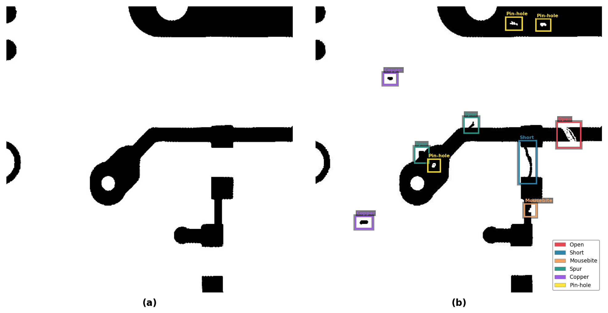
The DeepPCB dataset consists of 1500 image pairs curated for printed circuit board (PCB) defect detection, covering six defect categories: open circuits, short circuits, mouse bites, spurs, pinholes, and spurious copper traces. Each pair contains a defect-free template image and a defective test image, both segmented into sub-images of 640 × 640 pixels from original scans with a resolution of 16,000 × 16,000 pixels, acquired using linear scan CCD technology at 48 pixels per millimeter [56]. Of these, 1000 image pairs are allocated for training and 500 for testing. The images are aligned using a template matching technique to minimize offset errors; binarization is also applied to reduce illumination disturbances. The images with defects are annotated with axis-aligned bounding boxes containing class IDs for localization and classification tasks. Figure 10 depicts an example image with all six defect classes.

4.9. FICS PCB

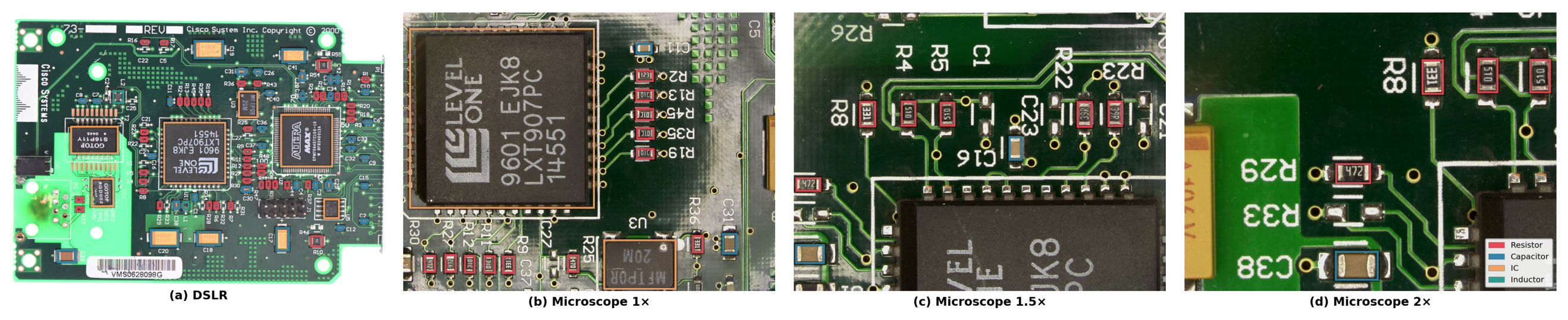
The dataset used is known as FICS-PCB [61], developed by the Security and Assurance (SCAN) lab at the University of Florida, and is a comprehensive resource that is designed to aid research on automated Printed Circuit Board (PCB) visual inspection systems. The dataset has a total of 9912 PCB component images captured using DSLR cameras with large CCD sensors and digital optical microscopes at various subsets, including 1×, 1.5×, and 2× ranges. These images are annotated with information on 77,347 components across six classes: capacitors, resistors, transistors, diodes, inductors, and integrated circuits (ICs). The annotations are then stored in CSV-formatted files, providing detailed metadata about components, their location, and type. Figure 11 provides a sample PCB image at full size, along with microscope tile images at 1×, 1.5×, and 2× magnification.

4.10. RF100 PCB

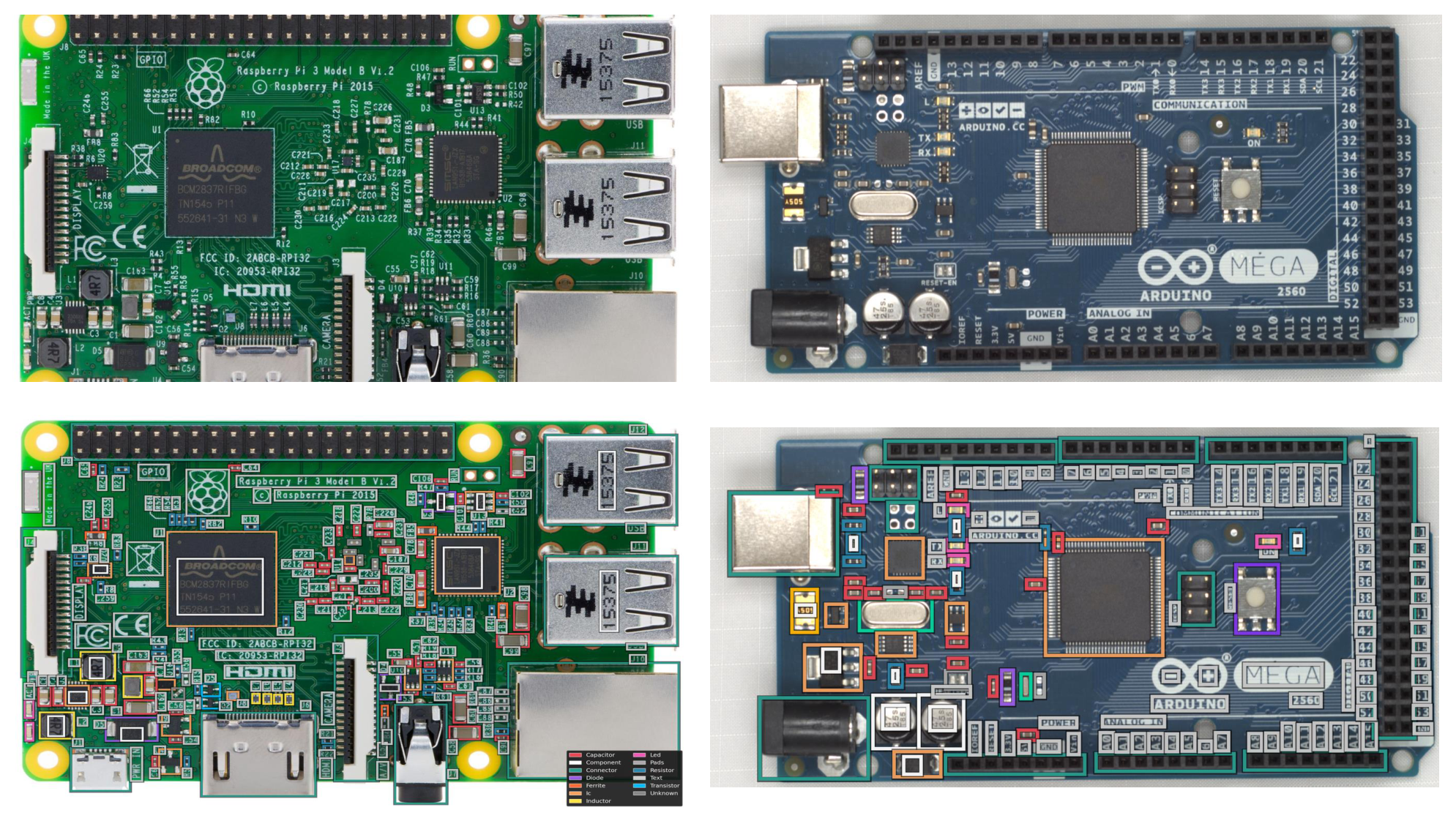
The dataset [62] belongs to the Roboflow 100 project, which contains 100 datasets covering multiple categories for object detection. The dataset has a total of 632 PCB component images, and is split into 82% training set, 12% validation set, and 7% test set. The dataset labels components into 34 classes. Figure 12 exhibits a sample image with bounding boxes for component classes.

5. AI and Computer Vision in Waste Sorting

Recent advances in artificial intelligence (AI) and computer vision have transformed the classification, management, and recycling of waste materials. Over the past decade, deep learning methods have evolved from prototype systems tested on small, controlled datasets to robust, real-time solutions capable of addressing the complexity of industrial environments. These advancements enable more accurate sorting and recycling processes, minimize human error, and support the global transition toward sustainable waste management. This section reviews the principal technical approaches that have driven progress in this field, including convolutional neural networks (CNNs), transformer-based architectures, real-time detection systems, and hybrid models.

5.1. Deep Learning for Waste Classification

At the core of most automated waste-sorting systems are convolutional neural networks (CNNs), which can automatically learn spatial and texture-based features from input images without requiring manual feature design. These networks identify patterns such as color, edges, and surface texture, which are essential cues for distinguishing between plastics, metals, paper, and glass.
Early efforts, such as those by Adedeji and Wang [64], achieved more than 85% accuracy on municipal solid waste datasets, demonstrating that CNNs could effectively categorize materials based on visual cues. Later, more advanced CNN architectures such as VGGNet, Inception, and ResNet further advanced network architectures and leveraged transfer learning to achieve accuracy above 90% on benchmark datasets, including TrashNet and Waste Classification Data [65]. CNNs remain the workhorse of computer vision-based waste classification, valued for their computational efficiency, straightforward training, and ability to deliver high performance even with modest data volumes.
However, the reliance of CNNs on local feature extraction limits the ability to understand context or relationships between distant regions within an image. This limitation becomes critical when sorting overlapping or visually similar materials.
To address these limitations, transformer-based architectures have been introduced. Unlike CNNs, transformers employ self-attention mechanisms that analyze global relationships across the entire image, capturing long-range dependencies and subtle interconnections that CNNs might overlook. Vision Transformer (ViT), for example, treats an image as a sequence of small patches and analyzes their relationships, similar to how natural language processing models interpret words in a sentence. Its improved context awareness makes it especially valuable for complex industrial waste environments. The Swin Transformer further refines this concept with a hierarchical shifted-window architecture that balances global reasoning with efficient computation, making it effective for both detection and segmentation tasks.
Transformer-based models generally outperform CNNs on complex recognition tasks, but their high computational cost and substantial data requirements make them less practical for low-power edge devices used in real-time sorting. CNN frameworks such as YOLOv5 provide a middle ground: they combine the efficiency of convolutional operations with sufficient contextual awareness for accurate detection. Hybrid models that integrate CNN backbones with transformer attention mechanisms, such as DETR variants, are emerging as a balance between performance and deployability.

5.1.1. Real-Time Object Detection Networks

While CNNs are effective for classification tasks, practical sorting systems must also localize objects within a scene. Real-time object detectors such as YOLO (You Only Look Once), SSD (Single Shot Multibox Detector), and Faster R-CNN achieve this by combining classification and localization in a single forward pass. Kumar et al. [66] demonstrated a YOLOv3 model that distinguishes biodegradable from non-biodegradable waste in real time at approximately 90% precision. Similarly, Huang and Wei [55] used YOLOv3 with MobileNet to identify PCB components, achieving 95.21% precision and processing each image in 0.079 s, demonstrating real-time capability for industrial applications.
However, real-time systems face challenges when recognizing very small or partially hidden items. Performance can drop when components overlap or when labeling quality is inconsistent. Despite these limitations, YOLO-based detectors have become integral to robotic waste sorting systems because of their responsiveness, scalability, and suitability for embedded computing.

5.1.2. Hybrid and Hierarchical Architectures

Recent studies have explored hybrid models that combine CNN-based feature extraction with hierarchical classification or attention modules. These architectures are particularly useful for fine-grained e-waste sorting tasks, where different PCB layouts, materials, or hazardous components must be identified. Chen et al. [67] proposed a hierarchical YOLOv5 model that improved recognition accuracy by 38% compared to the YOLOv5 baseline, using a coarse-to-fine strategy that first detects component regions and then resolves fine-grained subtype distinctions.
Although these systems enhance precision, their main drawbacks include increased computational cost and large annotation requirements. The multi-stage logic can also introduce cascading errors, where early-stage misclassifications affect later decisions. Nevertheless, they represent a step toward more intelligent, adaptive systems capable of learning relationships between materials and their functional or economic value. Table 7 summarizes representative deep learning architectures for waste and PCB classification discussed above, comparing their model category, dataset, classification granularity, reported accuracy, and principal trade-offs.

5.1.3. Evolution Toward Modern Architectures

The shift from traditional CNN-based pipelines to one-stage detectors signifies a major advancement in waste classification research. Modern models strive to better handle fine details, changing lighting conditions, and occlusions. Attention-based architectures such as ViT and Swin Transformer have emerged, offering global relational reasoning that goes beyond the local receptive fields of CNNs. Table 8 contrasts CNN-based and transformer-based models across the criteria most relevant to waste classification, including feature extraction, data requirements, robustness to occlusion, and real-time inference.
In summary, AI-driven computer vision systems are redefining the future of waste management. Traditional CNNs provide robust, efficient foundations for material recognition, while transformers introduce a new era of intelligent context modeling. Real-time detectors like YOLO bridge the gap between theoretical research and industrial deployment, and hybrid architectures promise more precise and scalable solutions. Together, these innovations are transforming manual, error-prone sorting into an intelligent, automated process that supports both environmental sustainability and the circular economy.

5.2. Vision Systems for E-Waste

Research focused specifically on e-waste detection and classification remains limited compared with research on general waste management. Yet the complex composition of electronic waste offers significant incentives for advanced vision systems to identify recyclable components, precious metals, and other recoverable materials.
Wang et al. [16] used a transfer-learning approach to classify broad e-waste categories—including PCBs, cables, and plastic housings—achieving 91% accuracy. Their method effectively separated macro-level categories but lacked intra-category sensitivity to PCB grade or composite type. Bose et al. [68] fused deep InceptionV4 features with color-histogram descriptors, reduced them via PCA, and classified ten device-level e-waste categories with a random forest, reaching 98.96% accuracy. The fused model outperformed its deep-only (96.79%) and histogram-only (94.46%) variants, confirming that color cues complement learned CNN features. Notably, the residual errors occurred between visually similar categories, reinforcing that RGB appearance alone is insufficient for fine-grained discrimination, which is the same barrier that motivates component-level and multispectral approaches for waste PCBs.
Reza et al. [17] developed a CNN approach for identifying small integrated circuits (ICs) on PCBs, exploring combinations of object detection strategies and loss-boosting methods to improve recognition of small objects. Zhao et al. [47] extended this work by systematically analyzing color, shape, and texture features for PCB component detection, finding that color-based features provided the highest generalization across diverse datasets and lighting conditions. More recent work continues to refine detector architectures for these small, densely packed targets. Elsharkawy [69] augmented YOLOv11 with multiscale attention and a refined IoU loss for high-precision defect detection on printed circuit boards, and Meng et al. [70] similarly improved YOLOv11 for surface-defect detection on electronic products. Together, these illustrate the ongoing adaptation of YOLO-family detectors to the recognition challenges of electronic components and PCBs.
Silva et al. [18] contributed the PCB-DSLR dataset of 748 RGB images from 165 waste boards and proposed the WPCB-EFA method, combining YOLOv3-based component recognition with economic assessment. It yielded a mean average precision (mAP) of 0.965 for IC detection. It introduced a financial-gain estimation model based on recoverable metals per board—the only published system that connects computer vision output directly to recycling economics.
Table 9 draws the representative studies into a single frame of reference, comparing model, dataset, objective, reported performance, and limitations. Despite these promising results, RGB-only vision systems remain fundamentally limited. The spectral range of visible light cannot reveal chemical composition differences between optically similar materials—copper traces versus aluminum, or FR4 substrates versus polymers. Consequently, integrating multispectral modalities with deep neural networks is critical to enable material-level classification, as reviewed in Section 3.

5.3. YOLO Family: A Comparative Analysis

The You Only Look Once (YOLO) family, introduced by Redmon et al. [71] in 2015, has become the de facto standard for real-time object detection in industrial applications. YOLO reframes detection as a single regression problem: an input image is divided into a grid, and a unified network simultaneously predicts bounding box coordinates, objectness scores, and class probabilities for all grid cells in a single forward pass. This single-stage design achieves inference speeds one to two orders of magnitude faster than two-stage detectors such as Faster R-CNN, at an accuracy cost that has narrowed substantially with each generation [72].
All YOLO architectures share a three-component structure: a backbone for hierarchical feature extraction; a neck for multiscale feature aggregation (FPN, PAN, or BiFPN); and a head for bounding-box regression and classification. The evolution from YOLOv1 to YOLOv12 represents continuous refinement of each component—from anchor-based to anchor-free designs, from NMS-dependent to NMS-free inference, and from pure convolutional to attention-augmented backbones [72]. Table 10 summarizes the key architectural innovations for each major version. The seven variants evaluated in Section 6 are marked with †.

5.4. Gaps and Limitations in Current Approaches

Despite progress in CNNs, transfer learning, and modern detection architectures, several critical challenges remain, preventing deep learning-based waste classification systems from achieving robust performance in industrial environments.
  • Dataset Quality and Real-World Variability: Most reported accuracies come from clean, laboratory-based datasets such as TrashNet or simulated PCB samples. These collections lack the environmental variability found in real recycling facilities, where lighting, angles, and surface contamination vary greatly. Additionally, class imbalances, where common but high-value materials such as PCBs are under-represented relative to bulk plastics, hinder generalization to industrially relevant scenarios.
  • Limitations of RGB-Based Imaging: Most current methods depend solely on RGB images, which offer limited information about material composition. Visually similar items—different polymer types, colored glass, or non-ferrous metal alloys—can appear nearly identical in the visible spectrum. Even advanced architectures cannot reliably distinguish such materials without additional spectral information. The Capacitor class in our benchmark (Section 6) achieves less than 9% mAP@0.5 across all tested models, providing direct empirical evidence that this is a structural input limitation rather than a model deficiency. Future systems must incorporate NIR, hyperspectral, or XRF modalities, as reviewed in Section 3.
  • Fine-Grained Recognition and Occlusion: Most models handle waste classification broadly and struggle with detailed recognition—identifying polymer subtypes or individual PCB component classes—particularly when objects overlap or are partially obscured. In recycling facilities, where components arrive fragmented and mixed, this limitation significantly reduces sorting reliability.
Taken together, these gaps motivate the structure of this review. The existing literature is fragmented: individual studies report different models on different datasets, under inconsistent evaluation protocols, and seldom distinguish the limitations of the sensing modality from those of the detector itself. This fragmentation makes it difficult to determine which architecture is genuinely suited to PCB recycling, or whether a given performance ceiling originates from the model or from the input data. Two elements of this review address that difficulty directly. The benchmark in Section 6 then places ten detectors under one common protocol, which isolates modality-driven limits, such as the persistent difficulty of the Capacitor class, from architecture-driven differences. A consolidated and empirically grounded synthesis of this kind is precisely what the current state of the field requires.

5.5. Model Interpretability and Generalization

Most current CNN and YOLO models act as black boxes, offering little insight into their decision-making processes. This lack of explainability reduces trust in critical systems that handle hazardous e-waste or must adhere to regulatory separation rules. Their ability to generalize across datasets or regions is also limited; a model trained on municipal waste in one region often performs poorly on datasets from another, owing to variations in material composition and packaging styles. Addressing these issues remains an open research direction rather than a solved capability. Explainable AI (XAI) methods such as Grad-CAM, SHAP, and attention rollout could expose which spectral or spatial features drive a prediction, and physics-informed networks that incorporate material properties, reflectance behavior, and degradation conditions could improve both transparency and cross-domain generalization. Establishing standardized XAI protocols for hazardous-material sorting is therefore identified here as a priority direction for future work.

5.6. Computational and Industrial Deployment Constraints

Industrial recycling systems require fast, energy-efficient, and high-capacity image processing. Most transformer-based and deep CNN architectures remain computationally intensive, making them difficult to deploy on embedded hardware or mobile robotic units. Even with high accuracy, inference latency can exceed acceptable real-time limits for conveyor-based sorting or robotic manipulation. Practical deployment requires compressed and quantized models that maintain accuracy while reducing computational load. Lightweight options such as YOLO, MobileNet, and EfficientNet show promise, but their performance across degraded real-world conditions still requires thorough validation.
In summary, current deep learning-based waste classification systems exhibit promising results under controlled conditions but continue to face major challenges in industrial adaptation. Addressing these gaps will require collaboration across disciplines, combining machine learning with materials science, optics, and embedded hardware design, to advance real-world waste-sorting automation and enable sustainable, data-driven recycling systems.

6. Benchmark: YOLO Family vs. State-of-the-Art Detectors

The review presented in Section 3, Section 4 and Section 5 establishes that the most critical open question in AI-driven PCB recycling is whether current detectors can achieve the precision and throughput required for industrial deployment on a challenging, class-imbalanced dataset. To address this question directly, seven YOLO variants are benchmarked, spanning YOLOv3 to YOLOv12s, against three representative state-of-the-art non-YOLO architectures: Faster R-CNN [82], RT-DETR-L [83], and RetinaNet [84]. All models are evaluated on the same dataset, hardware, and training protocol to ensure a fair comparison. A preliminary study in this direction explored ensemble combinations of YOLO models for semiconductor e-waste PCB detection [85]; the present benchmark broadens that scope to a like-for-like comparison of individual YOLO variants against representative non-YOLO detectors under a common protocol.

6.1. Experimental Setup

The Roboflow RF100 PCB dataset [62] is used, a publicly available benchmark comprising 620 RGB images of printed circuit boards at 640 × 640 pixel resolution. The dataset is split 80/20 into training and validation subsets. It contains four component classes that reflect the most economically and operationally significant categories in PCB recycling: integrated circuits (IC), capacitors, connectors, and electrolytic capacitors. Table 11 reports the instance-level class distribution. The dataset is severely class-imbalanced: the Capacitor class accounts for 65.6% of all instances (3630 out of 5536), while the Electrolytic Capacitor class accounts for only 3.0% (166 instances). This imbalance, combined with the high visual similarity among component types, constitutes a realistic and challenging evaluation setting for industrial recycling applications. All detectors were implemented in PyTorch (version 2.2.2) and trained and evaluated using the Ultralytics framework (version 8.4.14) on the hardware described above.
To ensure full reproducibility and a fair cross-architecture comparison, every model was trained under a common protocol: 100 epochs, an input resolution of 640 × 640 pixels, a batch size of 16, and initialization from COCO-pretrained weights. Rather than tuning each network individually, each model family was trained with its officially published default hyperparameters. The complete training configuration for all ten models is summarized in Table 12.
The YOLO variants share an identical configuration, optimized with SGD (initial learning rate 0.01, momentum 0.937, weight decay 5 × 10 4 ) under a linear schedule with a three-epoch warm-up, and the standard Ultralytics augmentation pipeline (Mosaic, HSV jitter, scaling, translation, horizontal flipping, RandAugment, and random erasing). The non-YOLO baselines follow their respective reference recipes: Faster R-CNN and RetinaNet use ResNet-50-FPN backbones trained with SGD, while RT-DETR-L uses the AdamW optimizer with a lower learning rate ( 1 × 10 4 ), as recommended for transformer-based detectors. Two configuration differences are noted for transparency: Faster R-CNN was trained at the torchvision default input resolution (shorter side 800 pixels) rather than 640 × 640, and the convolutional baselines use their native augmentation transforms. Both differences are conservative with respect to the central finding, as the higher input resolution favors Faster R-CNN. All reported inference-speed measurements were obtained on the same Apple M4 hardware to keep the efficiency comparison consistent. No test-time augmentation is applied. Model size is reported as the on-disk weight file in megabytes (MB). Inference speed is measured as single-image latency in milliseconds (ms) on the same hardware, and frames per second (FPS) is computed as 1000 divided by latency. No architecture received per-model hyperparameter tuning; all model families were trained with their published defaults under identical epochs, resolution, and protocol to ensure a fair comparison.
Five standard object detection metrics are reported: Formally, a predicted box B p is matched to a ground-truth box B g t through the Intersection over Union,
IoU ( B p , B g t ) = | B p B g t | | B p B g t | .
A prediction is a true positive (TP) when its IoU with a ground-truth box exceeds the evaluation threshold, a false positive (FP) otherwise, and an unmatched ground-truth box is a false negative (FN). Precision and recall are then
P = T P T P + F P ,   R = T P T P + F N .
The average precision (AP) of a class is the area under its precision–recall curve, and the mean average precision averages AP over the C classes,
AP = 0 1 P ( R )   d R ,   mAP = 1 C c = 1 C AP c .
mAP@0.5 evaluates this at a fixed IoU threshold of 0.5, whereas mAP@0.5:0.95 averages it over ten thresholds from 0.5 to 0.95 in steps of 0.05,
mAP @ [ 0.5 : 0.95 ] = 1 10 t { 0.50 ,   0.55 ,   ,   0.95 } mAP IoU = t .
Throughput is reported as FPS = 1000 / τ , where τ is the single-image latency in milliseconds.
The benchmarked detectors are trained with characteristic objectives. The YOLO one-stage detectors minimize a multi-task loss combining bounding-box regression, objectness, and classification terms,
L YOLO = λ box L box + λ obj L obj + λ cls L cls ,
in which the localization term uses the complete IoU (CIoU) loss
L box = 1 IoU + ρ 2 ( b , b g t ) c 2 + α v ,
where ρ ( b , b g t ) is the Euclidean distance between the predicted and ground-truth box centers, c is the diagonal length of the smallest box enclosing both, and v measures aspect-ratio consistency. Faster R-CNN, a two-stage detector, adds a region-proposal objectness loss to box-regression (smooth- L 1 ) and classification (cross-entropy) heads, while RetinaNet addresses foreground–background imbalance through the focal loss:
FL ( p t ) = α t ( 1 p t ) γ log ( p t ) ,
where p t is the predicted probability of the true class and γ down-weights well-classified examples. The transformer-based RT-DETR replaces anchors and non-maximum suppression with a set-prediction formulation built on multi-head self-attention,
Attention ( Q , K , V ) = softmax   Q K d k V ,
where Q, K, and V are the query, key, and value projections and d k is the key dimension; predicted and ground-truth objects are matched one-to-one by Hungarian assignment.

6.2. YOLO Family Results

Table 13 reports the full results for the seven YOLO variants evaluated on the RF100 PCB dataset.
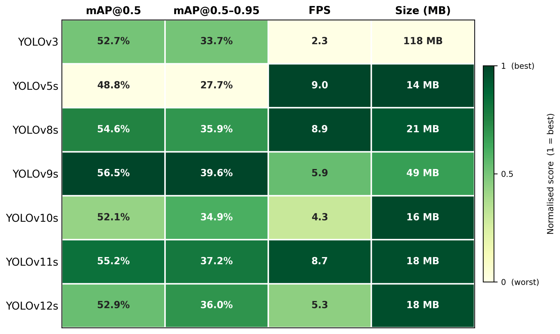
  • Accuracy. YOLOv9s achieves the highest mAP@0.5 (56.5%) and mAP@0.5–0.95 (39.6%) of all YOLO variants, as well as the highest precision (69.9%) and recall (54.4%). Its programmable gradient information (PGI) mechanism and GELAN backbone [72] appear to provide the most effective feature representation for the heterogeneous PCB component classes in this dataset. YOLOv11s achieves the second-best mAP@0.5 (55.2%) and mAP@0.5–0.95 (37.2%), making it the strongest candidate for deployment scenarios that prioritize both accuracy and efficiency. YOLOv8s ranks third on mAP@0.5 (54.6%) but achieves the highest recall among the mid-tier models (53.2%), making it preferable in applications that penalize false negatives.
  • Efficiency. YOLOv5s is the fastest model at 9.0 FPS and the smallest at 14 MB, but this comes at a significant accuracy cost: its mAP@0.5–0.95 of 27.7% is the lowest in the YOLO cohort, a 30% relative drop from YOLOv9s. YOLOv10s is paradoxically the slowest YOLO model evaluated (232 ms, 4.3 FPS) despite its NMS-free dual-assignment design, which was intended to improve inference speed. On this M4 CPU platform, the NMS-free inference graph does not yield lower latency than anchor-free models such as YOLOv8s and YOLOv11s.
  • Overall Performance. YOLOv11s represents the best accuracy–efficiency trade-off: at 115 ms (8.7 FPS) and only 18 MB, it delivers 55.2% mAP@0.5 and 37.2% mAP@0.5–0.95. Its compact footprint and competitive throughput make it the most viable candidate for edge-deployed conveyor sorting systems, where model size and real-time performance are primary constraints. YOLOv9s is the superior choice when peak accuracy is the priority and inference latency is less critical.
Figure 13 shows a normalized performance matrix across all seven YOLO models on the four evaluated dimensions (mAP@0.5, mAP@0.5–0.95, FPS, and model size).

6.3. State-of-the-Art Comparison

Across all evaluated configurations, the YOLO family consistently outperforms the SOTA baselines on most metrics, with faster detection speeds and smaller sizes. In Table 14, the best-performing YOLO model (YOLOv9s) is listed alongside three SOTA models: Faster R-CNN, RT-DETR-L, and RetinaNet. YOLOv9s achieves the highest mAP@0.5 among all models at 56.5%, followed by Faster R-CNN (46.7%), RetinaNet (35.6%), and RT-DETR-L (25.6%). Faster R-CNN achieves a more competitive mAP@0.5, trailing YOLOv9s by 9.8%; however, Faster R-CNN is much larger (330.2 MB vs. 49 MB), and its detection speed is much slower (0.14 FPS vs. 5.9 FPS). The highlight is that Faster R-CNN achieves the highest recall, 59.4%, among all models, but its precision (34.1%) is lower than YOLO’s, indicating a high rate of false-positive detections.
The lower accuracy of RT-DETR-L (25.6% mAP@0.5) compared to the YOLO models may be explained by certain issues inherent to the detection-transformer paradigm. One issue is the lack of spatial inductive bias in RT-DETR: no anchor priors, no locality biases. Therefore, all spatial relations have to be learned end-to-end using object queries and encoder-decoder attention. As discussed earlier, the lack of prior spatial knowledge slows down convergence. DETR needed about 500 training epochs to reach competitive accuracy on the COCO dataset [86], and Deformable DETR was proposed to address exactly this issue – slow convergence and low data efficiency [87]. Under the 100-epoch budget adopted here for parity with the YOLO models, the transformer is therefore far from convergence. Second, RT-DETR is trained end-to-end with a Hungarian bipartite matching loss that assigns exactly one query per ground-truth object. This one-to-one assignment provides far fewer positive learning signals per image than the dense grid assignment used by the YOLO detectors, and it becomes unstable when annotated instances are scarce, as in the 620-image RF100 PCB dataset. The per-class breakdown in Table 15 makes the effect clear. RT-DETR-L falls below YOLOv9s on every class, including the otherwise well-detected Electrolytic Capacitor class, where YOLOv9s reaches 91.6% but RT-DETR-L attains only 36.3%. This points to a global optimization and undertraining deficit rather than a single-class failure. Third, the advantages of RT-DETR over YOLO reported in the original work [83] were established on COCO-scale data, with roughly 118,000 training images. The benefits of global attention emerge only once tens of thousands of domain-specific images are available. The PCB-recycling domain currently lacks a dataset of this scale. This both explains the observed result and reinforces the central argument of this review, that realizing the potential of modern detection architectures in PCB recycling depends on the development of large-scale, standardized datasets.

6.4. Per-Class Performance Analysis

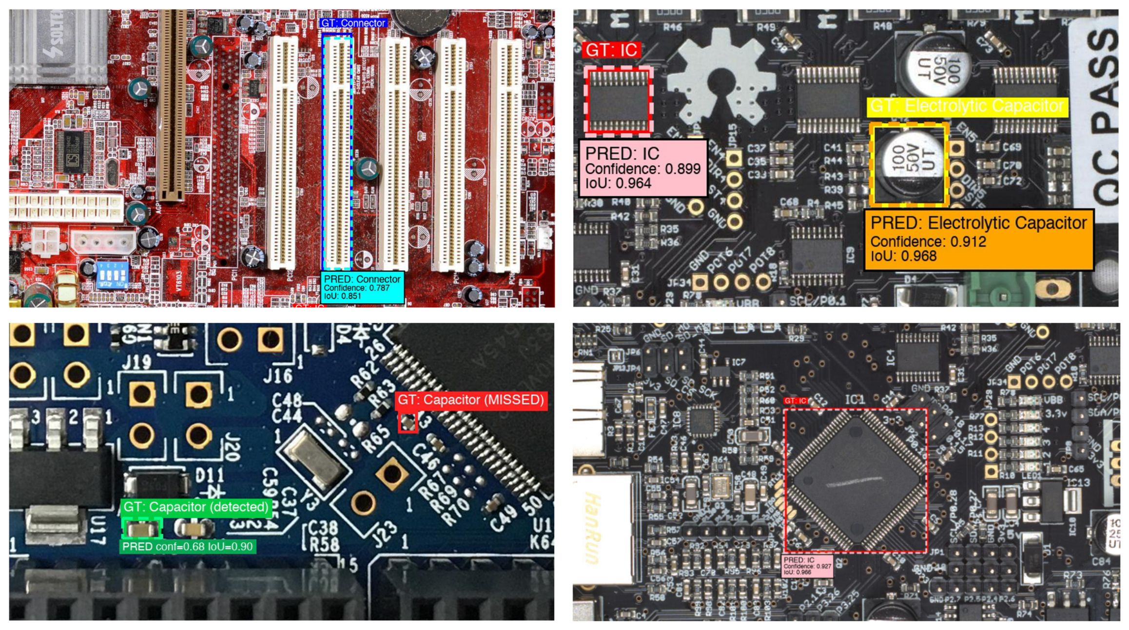
Table 16 reports the per-class mAP@0.5 for all seven YOLO models, and Table 15 extends the comparison to the three non-YOLO baselines using the best-performing YOLO variant (YOLOv9s) as a reference. Figure 14 shows sample detection results for YOLOv11s on the validation set.
For IC detection, YOLOv9s achieves the best mAP@0.5, with Faster R-CNN following closely at 59.4%. RetinaNet performs reasonably at 53.0%, suggesting that larger, visually distinctive components such as ICs are detectable across multiple architectures when trained appropriately. RT-DETR-L falls considerably further behind at 36.7%, consistent with transformer-based detectors struggling to generalize on small, domain-specific datasets.
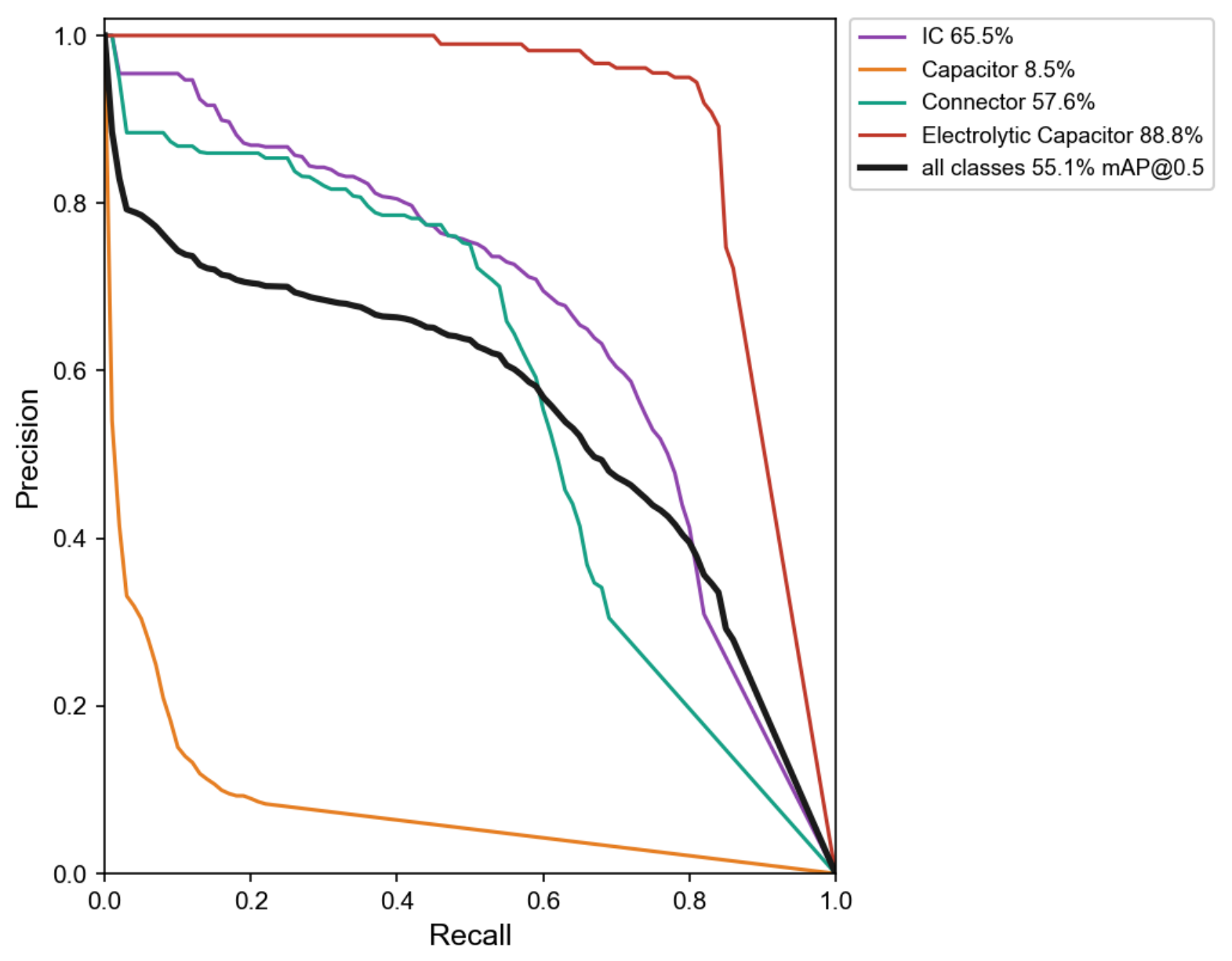
Detecting capacitors remains the most challenging across all models. Faster R-CNN outperforms YOLOv9s with 11.1% against 9.8%. Yet both predictions remain low for real-world practice. The performance of RT-DETR-L and RetinaNet is even worse. The difficulty stems from severe class imbalance: capacitors account for roughly two-thirds of all annotations, and they are also small in physical size and visually similar to PCB background textures. No evaluated architecture comes close to reliable detection on this class. Figure 15 shows the per-class Precision-Recall curves for YOLOv11s, illustrating the sharp divergence between the well-detected Electrolytic Capacitor and IC classes and the near-random performance on the Capacitor class.

7. Conclusions

This paper has presented a comprehensive review of AI-driven multispectral detection and classification for semiconductor e-waste recycling, organized around three distinct contributions that together map the current state of the field and the most critical directions for future work.
  • Contribution I: Material and Toxicological Context.
Section 2 established the material stakes of the recycling problem. Waste printed circuit boards contain up to 1000 times the gold concentration of primary ore and carry a recoverable value estimated at $57 billion per year globally, of which less than $10 billion is currently reclaimed. They simultaneously contain hazardous substances—lead, cadmium, hexavalent chromium, brominated flame retardants, and polychlorinated biphenyls—that contaminate recovery pathways and impose serious health risks for informal recycling workers. This dual character of value and hazard makes material-level sorting, rather than bulk shredding, the economically and environmentally necessary approach. It also establishes the upstream motivation for the sensing and detection technologies reviewed in the remainder of the paper.
  • Contribution II: Multispectral Sensing Review.
Section 3 reviewed four sensing modalities—RGB imaging, NIR spectroscopy, hyperspectral imaging (HSI), and X-ray fluorescence (XRF)—and characterized each by its operating principle, material discrimination capability, acquisition speed, and current state of integration with PCB recycling research. The central finding is that no single modality satisfies all requirements of an industrial sorting system. RGB provides the spatial resolution and throughput needed for conveyor deployment, but cannot resolve material composition at the molecular or elemental level. NIR and HSI extend material discrimination to polymer types and substrate chemistry but generate either insufficient information (NIR, for metals) or prohibitive data volumes (HSI, for real-time inference). XRF delivers quantitative elemental ground truth but is too slow for inline use. The reviewed literature contains no published system that fuses multiple modalities in a real-time PCB sorting pipeline—identifying this as the most significant open research gap in the field, and calling for the development of standardized multispectral PCB datasets as the prerequisite infrastructure.
  • Contribution III: Systematic Benchmark.
Section 6 reported the first systematic comparison of seven YOLO variants (YOLOv3 to YOLOv12s) against three representative non-YOLO detectors—Faster R-CNN, RT-DETR-L, and RetinaNet—on the RF100 PCB dataset under identical hardware and training conditions. YOLOv9s achieved the highest overall accuracy (mAP@0.5: 56.5%; mAP@0.5–0.95: 39.6%), while YOLOv11s provided the best balance of accuracy and efficiency (mAP@0.5: 55.2%, 115 ms, 18 MB) and is the most viable candidate for edge deployment. All non-YOLO baselines were substantially outperformed on both accuracy and throughput, confirming that, under default-hyperparameter training at this dataset scale, YOLO-family one-stage detectors are the appropriate architectural choice for resource-constrained industrial recycling applications. Transformer-based detection (RT-DETR-L) achieved only 25.6% mAP@0.5, indicating that transformer architectures require significantly larger domain-specific datasets before their architectural advantages are realized in the PCB recycling domain. It should be noted that all baselines were evaluated under their published default settings without per-architecture hyperparameter optimization; dedicated tuning, particularly for the transformer-based RT-DETR-L, which is sensitive to learning rate, warm-up, and schedule length, was beyond the scope of this benchmark and may narrow the reported gap. A fully tuned cross-architecture comparison is left to future work.
The single most consequential empirical finding of this review is the universal failure of all ten evaluated architectures on the Capacitor class: mAP@0.5 remains below 12% regardless of model family, parameter count, or training budget. Because the Capacitor class has 3630 annotated instances—the most abundant class in the dataset—this failure cannot be attributed to data scarcity. The root cause is a fundamental constraint of the visible spectrum: RGB imaging does not carry the molecular or elemental information needed to distinguish ceramic dielectric surfaces from epoxy substrates and metallic features at the PCB scale. This finding closes the loop between the sensing review and the benchmark: the path to industrially viable PCB recycling AI requires better sensors, not just better algorithms.
The transition from RGB-only to multispectral detection for PCB recycling is technically possible given the current sensor and fusion architectures. The key barriers are access to a large-scale multispectral database of PCBs obtained in realistic recycling settings, along with an engineering effort to build co-registered sensing equipment capable of being used on a conveyor belt. In such circumstances, it is likely that intermediate fusion approaches, like those described in Section 3.4, which combine spatial RGB information with NIR polymer characteristics or HSI spectral profiles through cross-modal attention, will provide a direct route toward detectors that can resolve the material classes that current systems cannot. Achieving this potential would substantially close the gap between the $57 billion in annually recoverable e-waste value and the less than $10 billion currently reclaimed, while simultaneously improving the safe identification and isolation of hazardous materials in global recycling streams.

Funding

This research received no external funding.

Data Availability Statement

The raw data supporting the conclusions of this article will be made available by the authors on request.

Conflicts of Interest

The authors declare no conflicts of interest.

Abbreviations

The following abbreviations are used in this manuscript:
ABSAcrylonitrile Butadiene Styrene
AIArtificial Intelligence
APAverage Precision
CCDCharge-Coupled Device
CLAHEContrast Limited Adaptive Histogram Equalization
CNNConvolutional Neural Network
CPUCentral Processing Unit
CRMCritical Raw Material
CRTCathode-Ray Tube
CSPCross Stage Partial (network)
DETRDetection Transformer
DPCBDiscarded Printed Circuit Board
DSLRDigital Single-Lens Reflex
ELANEfficient Layer Aggregation Network
FPNFeature Pyramid Network
FPSFrames Per Second
FR4Flame Retardant 4 (glass-reinforced epoxy laminate)
GELANGeneralized Efficient Layer Aggregation Network
HSIHyperspectral Imaging
ICIntegrated Circuit
IoUIntersection over Union
LIBSLaser-Induced Breakdown Spectroscopy
mAPmean Average Precision
MBMegabyte
NIRNear-Infrared
NMSNon-Maximum Suppression
PCBPrinted Circuit Board
PCBAPrinted Circuit Board Assembly
PEPolyethylene
PETPolyethylene Terephthalate
PGIProgrammable Gradient Information
PPPolypropylene
PVCPolyvinyl Chloride
R-CNNRegion-based Convolutional Neural Network
RF100Roboflow 100 (benchmark)
RGBRed, Green, Blue
RT-DETRReal-Time Detection Transformer
SMDSurface-Mount Device
SOTAState of the Art
VNIRVisible and Near-Infrared
WACVWinter Conference on Applications of Computer Vision
WEEEWaste Electrical and Electronic Equipment
WPCBWaste Printed Circuit Board
XAIExplainable Artificial Intelligence
XRFX-ray Fluorescence
YOLOYou Only Look Once

References

  1. United Nations University. The Global E-Waste Monitor 2024; United Nations University: Tokyo, Japan, 2024. [Google Scholar]
  2. Dzah, C.; O. Agyapong, J.; W. Apprey, M.; T. Agbevanu, K.; K. Kagbetor, P. Assessment of perceptions and practices of electronic waste management among commercial consumers in Ho, Ghana. Sustain. Environ. 2022, 8, 2048465. [Google Scholar] [CrossRef]
  3. Ramanayaka, S.; Keerthanan, S.; Vithanage, M. Urban mining of E-waste: Treasure hunting for precious nanometals. In Handbook of Electronic Waste Management; Elsevier: Amsterdam, The Netherlands, 2020; pp. 19–54. [Google Scholar]
  4. Olufokunbi, K.C.; Odejobi, O.A. A Computational Model For Electronic-Waste Dynamics. Ife J. Technol. 2018, 25, 39–44. [Google Scholar]
  5. Mir, M.A.; Chang, S.K. Saudi Arabia E-waste management strategies, challenges and opportunities, effect on health and environment: A strategic review. Emerg. Contam. 2024, 10, 100357. [Google Scholar] [CrossRef]
  6. World Health Organization. Electronic Waste (E-Waste); World Health Organization: Geneva, Switzerland, 2024. [Google Scholar]
  7. Bhattacharjee, J.; De, A.; Kamila, B.; Mandal, A. Recent scenario of e-waste recycling: Chemical engineering. Int. J. Chem. React. Eng. 2025, 23, 675–700. [Google Scholar] [CrossRef]
  8. Cabrera, R. Electronic Devices and Circuits; Scientific e-Resources: Delhi, India, 2019. [Google Scholar]
  9. Chalana, A.; Singh, K.; Sharma, S.; Bhardwaj, V.; Rai, R.K. E-waste Management: Prospects and Strategies. In Microbial Technology for Sustainable E-Waste Management; Debbarma, P., Kumar, S., Suyal, D.C., Soni, R., Eds.; Springer: Cham, Switzerland, 2023. [Google Scholar] [CrossRef]
  10. Van Yken, J.; Boxall, N.J.; Cheng, K.Y.; Nikoloski, A.N.; Moheimani, N.R.; Kaksonen, A.H. E-Waste Recycling and Resource Recovery: A Review on Technologies, Barriers and Enablers with a Focus on Oceania. Metals 2021, 11, 1313. [Google Scholar] [CrossRef]
  11. El-Sherif, D.M.; Abouzid, M.; Saber, A.N.; Hassan, G.K. A raising alarm on the current global electronic waste situation through bibliometric analysis, life cycle, and techno-economic assessment: A review. Environ. Sci. Pollut. Res. 2024, 31, 40778–40794. [Google Scholar] [CrossRef] [PubMed]
  12. Perfectson Oise, G.; Konyeha, S. Optimization of E-Waste Sorting Process Using Deep Learning. Radinka J. Sci. Syst. Lit. Rev. 2025, 3, 612–622. [Google Scholar] [CrossRef]
  13. Mohsin, M.; Rovetta, S.; Masulli, F.; Cabri, A. Automated Disassembly of Waste Printed Circuit Boards: The Role of Edge Computing and IoT. Computers 2025, 14, 62. [Google Scholar] [CrossRef]
  14. Shen, M.; Liu, Y.; Chen, J.; Ye, K.; Gao, H.; Che, J.; Wang, Q.; He, H.; Liu, J.; Wang, Y.; et al. Defect detection of printed circuit board assembly based on YOLOv5. Sci. Rep. 2024, 14, 70176. [Google Scholar] [CrossRef] [PubMed]
  15. Glučina, M.; Anđelić, N.; Lorencin, I.; Car, Z. Detection and classification of printed circuit boards using YOLO algorithm. Electronics 2023, 12, 667. [Google Scholar] [CrossRef]
  16. Wang, Y.; Deng, Y.; Zheng, Y.; Chattopadhyay, P.; Wang, L. Vision transformers for image classification: A comparative survey. Technologies 2025, 13, 32. [Google Scholar] [CrossRef]
  17. Reza, M.A.; Chen, Z.; Crandall, D.J. Deep neural network–based detection and verification of microelectronic images. J. Hardw. Syst. Secur. 2020, 4, 44–54. [Google Scholar] [CrossRef]
  18. Silva, L.H.d.S.; Júnior, A.A.; Azevedo, G.O.; Oliveira, S.C.; Fernandes, B.J. Estimating recycling return of integrated circuits using computer vision on printed circuit boards. Appl. Sci. 2021, 11, 2808. [Google Scholar] [CrossRef]
  19. Arbash, E.; Fuchs, M.; Rasti, B.; Lorenz, S.; Ghamisi, P.; Gloaguen, R. PCB-vision: A multiscene rgb-hyperspectral benchmark dataset of printed circuit boards. IEEE Sens. J. 2024, 24, 17140–17158. [Google Scholar] [CrossRef]
  20. Bressanelli, G.; Saccani, N.; Pigosso, D.C.; Perona, M. Circular Economy in the WEEE industry: A systematic literature review and a research agenda. Sustain. Prod. Consum. 2020, 23, 174–188. [Google Scholar] [CrossRef]
  21. Goyal, S.; Gupta, S. A comprehensive review of current techniques, issues, and technological advancements in sustainable E-waste management. E-Prime Electr. Eng. Electron. Energy 2024, 9, 100702. [Google Scholar] [CrossRef]
  22. Wu, C.; Awasthi, A.K.; Qin, W.; Liu, W.; Yang, C. Recycling value materials from waste PCBs focus on electronic components: Technologies, obstruction and prospects. J. Environ. Chem. Eng. 2022, 10, 108516. [Google Scholar] [CrossRef]
  23. Choubey, S.; Goswami, P.; Gautam, S. AI based sustainable approach for metal extraction from e-waste: A comprehensive literature review. In Proceedings of the 2020 3rd International Conference on Intelligent Sustainable Systems (ICISS); IEEE: New York, NY, USA, 2020; pp. 1445–1449. [Google Scholar]
  24. Roy, A.; Al Hasan, M.M.; Ghosh, S.; Varshney, N.; Julia, J.; Forghani, R.; Asadizanjani, N. Applications and challenges of ai in pcb x-ray inspection: A comprehensive study. ACM J. Emerg. Technol. Comput. Syst. 2025, 21, 1–28. [Google Scholar] [CrossRef]
  25. Ghelani, H. AI-Driven quality control in PCB manufacturing: Enhancing production efficiency and precision. Val. Int. J. Digit. Libr. 2024, 12, 1549–1564. [Google Scholar] [CrossRef]
  26. Alyammahi, H.S.M. The Role and the Limitation of AI Implementations in PCB Defect Detection. Master’s Thesis, Zayed University, Dubai, United Arab Emirates, 2025. [Google Scholar]
  27. Mohsin, M.; Rovetta, S.; Masulli, F.; Cabri, A. Artificial Intelligence Approach for Waste-Printed Circuit Board Recycling: A Systematic Review. Computers 2025, 14, 304. [Google Scholar] [CrossRef]
  28. Oke, E.A.; Potgieter, H. Discarded e-waste/printed circuit boards: A review of their recent methods of disassembly, sorting and environmental implications. J. Mater. Cycles Waste Manag. 2024, 26, 1277–1293. [Google Scholar]
  29. Kaya, M. Recovery of metals and nonmetals from electronic waste by physical and chemical recycling processes. Waste Manag. 2016, 57, 64–90. [Google Scholar] [CrossRef] [PubMed]
  30. Zarshenas, P.; AmirBeygi, M.; Haghbin, E.; Abdoos, M. A Review Study On A Polymer Optical Nanosensor Named» Pourya-Zar Sensor «For Detection Of ((As)) Heavy Metal Ions In Aquatic Environments. Int. J. Clin. Med. Case Rep. 2023, 7, 1–40. [Google Scholar]
  31. Patwa, J.; Sharma, A.; Flora, S.J.S. Arsenic, Cadmium, and Lead. In Reproductive and Developmental Toxicology, 3rd ed.; Gupta, R.C., Ed.; Academic Press: Cambridge, MA, USA, 2022; Chapter 29; pp. 547–571. [Google Scholar] [CrossRef]
  32. Nithya, R.; Sivasankari, C.; Thirunavukkarasu, A. Electronic waste generation, regulation and metal recovery: A review. Environ. Chem. Lett. 2021, 19, 1347–1368. [Google Scholar]
  33. Omondi, E.A.; Ndiba, P.K.; Koech, G.C. Complexity of E-Waste and Its Management Challenges in Developing Countries—A Review. Int. J. Environ. Sci. Nat. Resour. 2022, 31, 556309. [Google Scholar] [CrossRef]
  34. Nyeko, S.J.; Mlay, S.V.; Amerit, B.; Abima, B.; Among, J.; Nyero, A.I.; Odiya, J.; Ogen, C. The Impact of Electronic-Electrical Waste on Human Health and Environment: A Systematic Literature Review. J. Eng. Technol. Res. 2023, 15, 1–16. [Google Scholar] [CrossRef]
  35. Abdelbasir, S.M.; Kamel, A.H. Status of Electronic Waste Recycling Techniques: A Review. Environ. Sci. Pollut. Res. 2018, 25, 16533–16547. [Google Scholar] [CrossRef] [PubMed]
  36. Charitopoulou, M.A.; Kalogiannis, K.G.; Lappas, A.A.; Achilias, D.S. Novel Trends in the Thermo-Chemical Recycling of Plastics from WEEE Containing Brominated Flame Retardants. Environ. Sci. Pollut. Res. 2021, 28, 59190–59213. [Google Scholar] [CrossRef] [PubMed]
  37. Leung, A.O.W. Environmental contamination and health effects due to E-waste recycling. In Electronic Waste Management and Treatment Technology; Butterworth-Heinemann: Oxford, UK, 2019; pp. 335–362. [Google Scholar]
  38. Bonifazi, G.; Fiore, L.; Gasbarrone, R.; Hennebert, P.; Serranti, S. Detection of brominated plastics from e-waste by short-wave infrared spectroscopy. Recycling 2021, 6, 54. [Google Scholar]
  39. Serranti, S.; Bonifazi, G. Techniques for separation of plastic wastes. In Use of Recycled Plastics in Eco-Efficient Concrete; Elsevier: Amsterdam, The Netherlands, 2019; pp. 9–37. [Google Scholar]
  40. Ilyas, S.; Srivastava, R.R.; Kim, H.; Das, S.; Singh, V.K. Circular bioeconomy and environmental benignness through microbial recycling of e-waste: A case study on copper and gold restoration. Waste Manag. 2021, 121, 175–185. [Google Scholar] [CrossRef] [PubMed]
  41. Ruan, J.; Xu, Z. Constructing environment-friendly return road of metals from e-waste: Combination of physical separation technologies. Renew. Sustain. Energy Rev. 2016, 54, 745–760. [Google Scholar]
  42. Lu, Y.; Yang, B.; Gao, Y.; Xu, Z. An automatic sorting system for electronic components detached from waste printed circuit boards. Waste Manag. 2022, 137, 1–8. [Google Scholar] [CrossRef] [PubMed]
  43. Ravansari, R.; Wilson, S.C.; Tighe, M. Portable X-ray fluorescence for environmental assessment of soils: Not just a point and shoot method. Environ. Int. 2020, 134, 105250. [Google Scholar] [CrossRef] [PubMed]
  44. Ichikawa, S.; Hirokawa, Y.; Kurisaki, T.; Nakamura, T. Characterization of a printed-circuit board by X-ray fluorescence and X-ray diffraction analyses for metal recovery. Spectrochim. Acta Part B At. Spectrosc. 2023, 210, 106819. [Google Scholar]
  45. Ferreira, D.S.; Pereira, F.M.; Olivieri, A.C.; Pereira-Filho, E.R. Electronic waste analysis using laser-induced breakdown spectroscopy (LIBS) and X-ray fluorescence (XRF): Critical evaluation of data fusion for the determination of Al, Cu and Fe. Anal. Chim. Acta 2024, 1303, 342522. [Google Scholar] [PubMed]
  46. Picón, A.; Ghita, O.; Whelan, P.F.; Iriondo, P.M. Fuzzy spectral and spatial feature integration for classification of nonferrous materials in hyperspectral data. IEEE Trans. Ind. Inform. 2009, 5, 483–494. [Google Scholar] [CrossRef]
  47. Zhao, W.; Gurudu, S.R.; Taheri, S.; Ghosh, S.; Mallaiyan Sathiaseelan, M.A.; Asadizanjani, N. PCB component detection using computer vision for hardware assurance. Big Data Cogn. Comput. 2022, 6, 39. [Google Scholar] [CrossRef]
  48. Gundupalli, S.P.; Hait, S.; Thakur, A. Classification of metallic and non-metallic fractions of e-waste using thermal imaging-based technique. Process Saf. Environ. Prot. 2018, 118, 32–39. [Google Scholar]
  49. Hussein, A.F.; Hamanah, W.M.; Abido, M.A. Harnessing hyperspectral imaging and deep learning for advanced e-waste classification using three spectral bands. Results Eng. 2025, 27, 106110. [Google Scholar] [CrossRef]
  50. Moroni, M.; Balsi, M.; Bouchelaghem, S. Plastics detection and sorting using hyperspectral sensing and machine learning algorithms. Waste Manag. 2025, 203, 114854. [Google Scholar] [CrossRef] [PubMed]
  51. Ramachandram, D.; Taylor, G.W. Deep multimodal learning: A survey on recent advances and trends. IEEE Signal Process. Mag. 2017, 34, 96–108. [Google Scholar] [CrossRef]
  52. Radford, A.; Kim, J.W.; Hallacy, C.; Ramesh, A.; Goh, G.; Agarwal, S.; Sastry, G.; Askell, A.; Mishkin, P.; Clark, J.; et al. Learning transferable visual models from natural language supervision. In Proceedings of the International Conference on Machine Learning, PMLR, Virtual, 18–24 July 2021; pp. 8748–8763. [Google Scholar]
  53. Alayrac, J.B.; Donahue, J.; Luc, P.; Miech, A.; Barr, I.; Hasson, Y.; Lenc, K.; Mensch, A.; Millican, K.; Reynolds, M.; et al. Flamingo: A visual language model for few-shot learning. Adv. Neural Inf. Process. Syst. 2022, 35, 23716–23736. [Google Scholar] [CrossRef]
  54. Liang, P.P.; Zadeh, A.; Morency, L.P. Foundations & trends in multimodal machine learning: Principles, challenges, and open questions. ACM Comput. Surv. 2024, 56, 1–42. [Google Scholar] [CrossRef]
  55. Huang, W.; Wei, P. A PCB dataset for defects detection and classification. arXiv 2019, arXiv:1901.08204. [Google Scholar]
  56. Tang, S.; He, F.; Huang, X.; Yang, J. Online PCB defect detector on a new PCB defect dataset. arXiv 2019, arXiv:1902.06197. [Google Scholar]
  57. Makwana, D.; Teja R., S.C.; Mittal, S. PCBSegClassNet—A light-weight network for segmentation and classification of PCB component. Expert Syst. Appl. 2023, 225, 120029. [Google Scholar]
  58. Pramerdorfer, C.; Kampel, M. A dataset for computer-vision-based PCB analysis. In Proceedings of the 2015 14th IAPR International Conference on Machine Vision Applications (MVA); IEEE: New York, NY, USA, 2015; pp. 378–381. [Google Scholar]
  59. Mahalingam, G.; Gay, K.M.; Ricanek, K. Pcb-metal: A pcb image dataset for advanced computer vision machine learning component analysis. In Proceedings of the 2019 16th International Conference on Machine Vision Applications (MVA); IEEE: New York, NY, USA, 2019; pp. 1–5. [Google Scholar]
  60. Kuo, C.W.; Ashmore, J.D.; Huggins, D.; Kira, Z. Data-efficient graph embedding learning for PCB component detection. In Proceedings of the 2019 IEEE Winter Conference on Applications of Computer Vision (WACV); IEEE: New York, NY, USA, 2019; pp. 551–560. [Google Scholar]
  61. Lu, H.; Mehta, D.; Paradis, O.; Asadizanjani, N.; Tehranipoor, M.; Woodard, D.L. Fics-pcb: A Multi-Modal Image Dataset for Automated Printed Circuit Board Visual Inspection. Cryptology ePrint Archive, Paper 2020/366. 2020. Available online: https://eprint.iacr.org/2020/366 (accessed on 22 June 2026).
  62. Roboflow 100. Printed Circuit Board Dataset. 2024. Available online: https://universe.roboflow.com/roboflow-100/printed-circuit-board (accessed on 14 November 2025).
  63. Jessurun, N.; Dizon-Paradis, O.P.; Harrison, J.; Ghosh, S.; Tehranipoor, M.M.; Woodard, D.L.; Asadizanjani, N. FPIC: A novel semantic dataset for optical PCB assurance. ACM J. Emerg. Technol. Comput. Syst. 2023, 19, 1–21. [Google Scholar] [CrossRef]
  64. Adedeji, O.; Wang, Z. Intelligent waste classification system using deep learning convolutional neural network. Procedia Manuf. 2019, 35, 607–612. [Google Scholar] [CrossRef]
  65. Yang, M.; Thung, G. Classification of trash for recyclability status. CS229 Proj. Rep. 2016, 2016, 3. [Google Scholar] [CrossRef]
  66. Kumar, S.; Yadav, D.; Gupta, H.; Verma, O.P.; Ansari, I.A.; Ahn, C.W. A novel yolov3 algorithm-based deep learning approach for waste segregation: Towards smart waste management. Electronics 2020, 10, 14. [Google Scholar] [CrossRef]
  67. Chen, J.; Bao, E.; Pan, J. Classification and positioning of circuit board components based on improved YOLOv5. Procedia Comput. Sci. 2022, 208, 613–626. [Google Scholar] [CrossRef]
  68. Bose, N.S.C.; Kumaraswamy, I.; Krishna, N.H.; Reddy, T.R.S.; Sudhakar, P.; Krishnan, G.H. Integrating InceptionV4 and Color Histogram for Scalable E-Waste Classification Framework. In Proceedings of the 2025 International Conference on Innovative Trends in Information Technology (ICITIIT); IEEE: New York, NY, USA, 2025; pp. 1–4. [Google Scholar]
  69. Elsharkawy, Z.F. Enhanced YOLOv11 framework for high precision defect detection in printed circuit boards. Sci. Rep. 2025, 15, 42550. [Google Scholar] [CrossRef] [PubMed]
  70. Meng, J.; Guo, L.; Hao, W.; Jain, D.K. A surface defect detection method for electronic products based on improved YOLOv11. PLoS ONE 2025, 20, e0334333. [Google Scholar] [CrossRef] [PubMed]
  71. Redmon, J.; Divvala, S.; Girshick, R.; Farhadi, A. You only look once: Unified, real-time object detection. In Proceedings of the IEEE Conference on Computer Vision and Pattern Recognition; IEEE: New York, NY, USA, 2016; pp. 779–788. [Google Scholar]
  72. Jegham, N.; Koh, C.Y.; Abdelatti, M.; Hendawi, A. Yolo evolution: A comprehensive benchmark and architectural review of yolov12, yolo11, and their previous versions. arXiv 2024, arXiv:2411.00201. [Google Scholar]
  73. Redmon, J.; Farhadi, A. YOLO9000: Better, faster, stronger. In Proceedings of the IEEE Conference on Computer Vision and Pattern Recognition; IEEE: New York, NY, USA, 2017; pp. 7263–7271. [Google Scholar]
  74. Redmon, J.; Farhadi, A. Yolov3: An incremental improvement. arXiv 2018, arXiv:1804.02767. [Google Scholar]
  75. Bochkovskiy, A.; Wang, C.Y.; Liao, H.Y.M. Yolov4: Optimal speed and accuracy of object detection. arXiv 2020, arXiv:2004.10934. [Google Scholar]
  76. Li, C.; Li, L.; Jiang, H.; Weng, K.; Geng, Y.; Li, L.; Ke, Z.; Li, Q.; Cheng, M.; Nie, W.; et al. YOLOv6: A single-stage object detection framework for industrial applications. arXiv 2022, arXiv:2209.02976. [Google Scholar]
  77. Wang, C.Y.; Bochkovskiy, A.; Liao, H.Y.M. YOLOv7: Trainable bag-of-freebies sets new state-of-the-art for real-time object detectors. In Proceedings of the IEEE/CVF Conference on Computer Vision and Pattern Recognition; IEEE: New York, NY, USA, 2023; pp. 7464–7475. [Google Scholar]
  78. Wang, C.Y.; Yeh, I.H.; Mark Liao, H.Y. Yolov9: Learning what you want to learn using programmable gradient information. In Proceedings of the European Conference on Computer Vision; Springer: Berlin/Heidelberg, Germany, 2024; pp. 1–21. [Google Scholar]
  79. Wang, A.; Chen, H.; Liu, L.; Chen, K.; Lin, Z.; Han, J.; Ding, G. Yolov10: Real-time end-to-end object detection. Adv. Neural Inf. Process. Syst. 2024, 37, 107984–108011. [Google Scholar] [CrossRef]
  80. Khanam, R.; Hussain, M. Yolov11: An overview of the key architectural enhancements. arXiv 2024, arXiv:2410.17725. [Google Scholar]
  81. Tian, Y.; Ye, Q.; Doermann, D. Yolov12: Attention-centric real-time object detectors. arXiv 2025, arXiv:2502.12524. [Google Scholar]
  82. Ren, S.; He, K.; Girshick, R.; Sun, J. Faster r-cnn: Towards real-time object detection with region proposal networks. Adv. Neural Inf. Process. Syst. 2015, 28, 1–9. [Google Scholar]
  83. Zhao, Y.; Lv, W.; Xu, S.; Wei, J.; Wang, G.; Dang, Q.; Liu, Y.; Chen, J. Detrs beat yolos on real-time object detection. In Proceedings of the IEEE/CVF Conference on Computer Vision and Pattern Recognition; IEEE: New York, NY, USA, 2024; pp. 16965–16974. [Google Scholar]
  84. Lin, T.Y.; Goyal, P.; Girshick, R.; He, K.; Dollár, P. Focal loss for dense object detection. In Proceedings of the IEEE International Conference on Computer Vision; IEEE: New York, NY, USA, 2017; pp. 2980–2988. [Google Scholar]
  85. Zhou, X.; Agaian, S. Ensemble Learning Using YOLO Models for Semiconductor E-Waste Recycling. Information 2026, 17, 322. [Google Scholar] [CrossRef]
  86. Carion, N.; Massa, F.; Synnaeve, G.; Usunier, N.; Kirillov, A.; Zagoruyko, S. End-to-end object detection with transformers. In Proceedings of the European Conference on Computer Vision; Springer: Berlin/Heidelberg, Germany, 2020; pp. 213–229. [Google Scholar]
  87. Zhu, X.; Su, W.; Lu, L.; Li, B.; Wang, X.; Dai, J. Deformable detr: Deformable transformers for end-to-end object detection. arXiv 2020, arXiv:2010.04159. [Google Scholar]
Figure 1. End-to-end conceptual framework for AI-driven multispectral PCB e-waste sorting. The pipeline runs through six stages: multi-sensor acquisition (RGB, NIR, HSI, XRF; Section 3), preprocessing and co-registration, sensor fusion (Section 3.4), detection and classification (Section 5 and Section 6), economic decision and output streams, and robotic actuation.
Machines 14 00730 g001
Figure 2. Material composition of (a) a representative bulk e-waste stream and (b) PCB-specific composition by mass fraction. Data from [10,29].
Machines 14 00730 g002
Figure 3. Comparison of sensing modalities for e-waste PCB recycling. The visible RGB window (400–700 nm) provides spatial resolution but cannot resolve material composition. NIR and VNIR bands (400–2500 nm) identify polymer types via molecular bond vibrations. Hyperspectral imaging extends NIR to full per-pixel spectral maps. XRF operates on X-ray excitation to deliver quantitative elemental composition independent of surface reflectance. No single modality satisfies all requirements; sensor fusion is the necessary next step.
Machines 14 00730 g003
Figure 4. (1) The Original PCB Image; (2) R Channel of the Image; (3) G Channel of the Image; (4) B Channel of the Image.
Machines 14 00730 g004
Figure 5. PCB defect detection example from the PCB-Defect dataset [55]. (Left): original RGB image. (Right): ground-truth bounding boxes for three missing hole defects.
Machines 14 00730 g005
Figure 6. Sample image from the PCB-Vision dataset and its respective masks: (a) RGB original image; (b) RGB general mask; (c) RGB monoseg mask [19].
Machines 14 00730 g006
Figure 7. Ground-truth annotations from dataset [58]: (a) original image; (b) rotated bounding boxes color-coded by component class; (c) binary segmentation mask rendered as solid white regions on a black background.
Machines 14 00730 g007
Figure 8. FPIC component dataset with a 768 × 768 patch sample [57]. (a) CLAHE-enhanced HSI capture; (b) ground-truth mask with colors denoting component classes.
Machines 14 00730 g008
Figure 9. Ground-truth component annotations on two representative PCBs. (Top row): original RGB images. (Bottom row): color-coded bounding boxes by component class [60].
Machines 14 00730 g009
Figure 10. Ground-truth annotations from the DeepPCB dataset: (a) defect-free template image; (b) corresponding test image with bounding boxes color-coded by defect class—Open, Short, Mousebite, Spur, Copper, and Pin-hole [56].
Machines 14 00730 g010
Figure 11. Sample annotations from the dataset: (a) full DSLR image with ground-truth bounding boxes (yellow, IC; blue, capacitors; red, resistors).; (bd) microscope tile images at 1×, 1.5×, and 2× magnification, demonstrating the dataset’s multiscale acquisition capability [61].
Machines 14 00730 g011
Figure 12. Sample RF100 PCB image with bounding boxes for component classes [62].
Machines 14 00730 g012
Figure 13. Normalized performance matrix for seven YOLO variants on the RF100 PCB dataset. Each metric is normalized to the [ 0 ,   1 ] range across the model cohort. Darker shading indicates better relative performance. YOLOv9s leads on accuracy metrics. YOLOv5s leads on speed and size; YOLOv11s achieves the most balanced profile.
Machines 14 00730 g013
Figure 14. Sample detection results for YOLOv11s on the RF100 PCB validation set. Solid boxes indicate ground-truth annotations; dashed boxes indicate model predictions.
Machines 14 00730 g014
Figure 15. Per-class Precision-Recall curves for YOLOv11s.
Machines 14 00730 g015
Table 1. Metal composition (wt%) of DPCBs from different device types. Dashes indicate values not reported. Data from [28].
Device TypeCuAlFeSnNiPbAgAuPd
Desktop computer14.5–52.41.0–9.60.1–3.41.0–10.30.03–0.260.07–5.00.010.0050.007
Desktop computer (CPU)30.59.49.41.83.60.830.13
Mobile phones27.8–47.91.4–3.70.4–2.30.02–3.20.6–2.90.3–1.60.01–0.470.02–0.140.007–0.04
Printers32.53.71.40.960.340.00.310.004
Televisions10.0–14.44.1–10.05.0–28.03.60.24–0.301.0–2.20.03–0.040.0020.001
Copy/fax machines21.0–21.35.1–6.14.8–6.62.5–3.00.35–0.571.3–1.80.13–0.14
Table 2. Common toxic substances in e-waste and their health impacts. Adapted from [30,31,33,34,35,36,37].
SubstanceSource in E-WasteHealth Consequences
Lead (Pb)Solder, semiconductor chips, PCBsNeurological damage, blood disorders, gastric ulcers; no safe threshold [30,31]
Mercury (Hg)Switch relays, fluorescent lampsBrain, liver, and kidney damage; bioaccumulates in aquatic food chains [33,34]
Cadmium (Cd)Semiconductor chips, batteriesIARC Group 1 carcinogen; kidney and bone damage; fetal neurodevelopmental defects [31,35]
Arsenic (As)Doping agent in semiconductors, LEDsBladder cancer, cardiovascular disease, liver, and renal disease [31]
Nickel (Ni)Batteries, PCBs, CRT tubesVomiting, convulsions, coma, or death [34]
Lithium (Li)Batteries, PCBs, CRT tubesGastrointestinal effects; chronic exposure linked to cancer [34]
BFRs, PBDEs, TBBPAFlame retardants in PCBs, plastic casingsHormonal disorders; endocrine and thyroid disruption on combustion [36]
POPsPrinted circuit boardsImmune suppression, neurodevelopmental issues, liver, and skin cancer [37]
Table 3. Potential values of key metals in e-waste generated globally in 2019 [10].
MetalAmount Present in E-Waste (kt)Potential Values (US $Million)
Gold (Au)0.29481
Iron (Fe)20,46624,645
Silver (Ag)1.2579
Palladium (Pd)0.13532
Copper (Cu)180810,960
Table 4. Comparison of sensing modalities for PCB e-waste sorting. Adapted from [19,39,43,44,45].
ModalityWavelength/RangeWhat It DetectsAdvantagesLimitations
RGB400–700 nm (visible)Color, shape, textureLow cost, fast, widely available; intuitive for spatial detectionCannot distinguish visually similar materials (solder types, polymer grades, FR4 variants); sensitive to lighting
NIR700–2500 nmMolecular bond vibrations; polymer types>95% polymer discrimination (PE, PP, PET, PVC); non-destructive; real-time capableLimited for metals and inorganic materials; requires controlled illumination
HSI400–1000 nm (VNIR); wider ranges availableFull spectral signature per pixel; material-level classification23% accuracy gain over RGB for PCB components [46]; pixel-level discriminationHigh data volume; computationally intensive; limited real-time deployment at conveyor speeds
XRFX-ray fluorescence (Na to U)Elemental composition (Cu, Au, Ag, Pb, Br, etc.)Non-destructive; quantitative; detects bromine in flame retardants; near-instant field resultsSurface-only analysis; no molecular/isotopic data; poor sensitivity for light elements (Z < 11); scan speed limits throughput
Table 5. Engineering practicability of the three sensor-fusion strategies under PCB-recycling industrial constraints.
StrategyConveyor-Speed ToleranceSynchronization RequirementIllumination/Vibration RobustnessEdge-Compute FootprintExpected Accuracy
Early fusionHighHigh (raw-level spatial/spectral alignment)LowLow–moderateModerate (alignment-limited)
Late fusionHigh (if parallelized)Low (tolerant of desynchronization)HighModerate–high (N full networks; distributable)Moderate (no cross-modal correlation)
Intermediate fusionLow–moderateHigh (pixel-level co-registration, sub-frame sync)Low–moderateHighHigh
Table 6. Summary of existing datasets.
DatasetPCB CountData VolumeData TypeDerivativesInspected ObjectsSensor TypeOpen-Source
V-PCB [13]--RGB Images (up to 1920 × 1920 )Lighting, orientation, distance, shadow, viewpoint, resolution variationsCapacitors, ICs, electrolytic capacitors, resistors, diodes, transistors, coils, transformersArducam 12.4 MP + NVIDIA Jetson NanoNo
PCBA-defect [55]-1386RGB Images-6 trace defectsDigital microscopeYes https://github.com/Ironbrotherstyle/PCB-DATASET?tab=readme-ov-file accessed on 22 June 2026
DeepPCB [56]-1500Binary Images-6 trace defectsLinear scan CCDYes https://github.com/tangsanli5201/DeepPCB accessed on 22 June 2026
FPIC [57]93 (261 total images)71,000+ annotationsRGB ImagesFront and back images; multiple settingsText annotations and mounted components (e.g., IC, resistors, SMDs)Nikon D850 DSLRYes https://physicaldb.ece.ufl.edu/index.php/fics-pcb-image-collection-fpic/ accessed on 22 June 2026
PCB-DSLR [58]165748RGB ImagesRotationPCB + (IC)DSLRYes https://cvl.tuwien.ac.at/research/cvl-databases/pcb-dslr-dataset/ accessed on 22 June 2026
PCB-Metal [59]123984RGB Images4 rotations + front and back scansIC, capacitors, resistors, inductorsDSLRNo
WACV PCB [60]4762,000 labelsRGB Images-31 distinct typesDSLRYes https://sites.google.com/view/chiawen-kuo/home/pcb-component-detection accessed on 22 June 2026
FICS-PCB [61]319912RGB ImagesIllumination, scale, sensorCapacitor, resistor, inductor, transistor, diode, ICDSLR + Digital microscopeNo
PCB-Vision [19]53106RGB Images + HyperspectralOptional derivatives providedPCB + (IC, capacitor, connectors)DSLR + Linescan SpectrometerYes https://rodare.hzdr.de/record/2704 accessed on 22 June 2026
RF100 PCB [62]632106RGB Images-IC, Electrolytic Capacitors, Tantalum Capacitors, Large MLCCs, Connector Blocks-Yes https://universe.roboflow.com/roboflow-100/printed-circuit-board accessed on 22 June 2026
Table 7. Representative deep learning architectures for waste classification.
CategoryModel/ReferenceDatasetClassification TypeAccuracy, (%)AdvantagesDisadvantages
CNN-basedAdedeji & Wang [64]Municipal wasteCoarse-grained87Simple, reliableSensitive to lighting
Transfer LearningYang & Thung [65]TrashNetCoarse-grained92–95Easy fine-tuningPoor real-world adaptation
Object DetectionKumar et al. [66]; YOLOv3Garbage datasetBinary (bio/non-bio)∼90Real-time accuracyMisses small objects
Object DetectionHuang et al. [55]; YOLOv3+MobileNetPCB datasetComponent detection95.21Fast inferenceIgnores occlusions
Hybrid/HierarchicalChen et al. [67]; YOLOv5+hierarchyPCB dismantlingFine-grained+38 over baselineHigh precisionHigh annotation demand
Table 8. Comparison between CNN-based and transformer-based waste classification models.
CriterionCNN Models (ResNet, YOLOv5)Transformer Models (ViT, Swin)
Feature ExtractionLocal texture and spatial filtersGlobal attention across patches
Data RequirementModerateHigh (requires large datasets)
Training ComplexityRelatively lowHigh; longer convergence time
Accuracy on Small DatasetsHighModerate
Robustness to OcclusionLimitedStrong contextual reasoning
Real-Time InferenceFast and efficientComputationally demanding
Adaptability to New CategoriesEasy transfer learningDepends on dataset diversity
Application to WasteOn-site sorting, defect detectionComplex scene understanding, fine-grained recognition
Table 9. Comparison of representative studies in e-waste and PCB detection.
StudyModelDatasetObjectiveAccuracy/mAPKey ContributionLimitation
Wang et al. [16]Transfer learning (ResNet)E-waste (mixed)Macro-category classification91%Broad sorting (PCB, cable, plastics)No intra-class differentiation
Reza et al. [17]Custom CNN + fast boostingPCB datasetTiny IC detection∼88%Enhanced small-object detectionNo material context
Zhao et al. [47]Feature-based detectionMulti-set PCB imagesFeature evaluationNot reportedColor features most informativeLimited spectral scope
Silva et al. [18]YOLOv3 (WPCB-EFA)PCB-DSLR (748 RGB)IC detection + value estimationmAP = 0.965Vision–economic model integrationRGB-only sensing
Mohsin et al. [27]YOLOv8/v9/v10/v11WPCB datasetComponent detection99.8% AP, 99.5% F1Multi-variant YOLO evaluationControlled setup; pristine boards
Bose et al. [68]InceptionV4 + color histogram + RFE-Waste (Kaggle, 10 classes)Device-level classification98.96%Fuses deep and hand-crafted color featuresDevice-level only; no component or spectral detail
Table 10. Comprehensive comparison of YOLO versions (v1–v12). Models benchmarked in Section 6 are marked with .
VersionYearBackboneKey InnovationRef.
YOLOv12015Darknet-24Single-stage grid regression; unified detection pipeline[71]
YOLOv22016Darknet-19Anchor boxes; batch normalization; multiscale training[73]
YOLOv3 2018Darknet-53Multiscale FPN predictions; residual backbone[74]
YOLOv42020CSPDarknet-53Mosaic augmentation; CIoU loss; PANet neck[75]
YOLOv5s 2020Modified CSPv7PyTorch framework; SPPF; auto-anchor; AutoML[72]
YOLOv62022EfficientRepRepVGG blocks; re-parameterization at inference[76]
YOLOv72022E-ELANExtended ELAN; auxiliary training heads[77]
YOLOv8s 2023Modified CSPv7Anchor-free decoupled head; C2f module[72]
YOLOv9s 2024GELANProgrammable gradient information (PGI)[78]
YOLOv10s 2024Modified CSPNMS-free dual-assignment; one-to-one inference head[79]
YOLO11s 2024C3k2 + C2PSACSP bottleneck with self-attention; GFLOPs-optimal[80]
YOLOv12s 2025R-ELANArea Attention (A2); residual ELAN[81]
Table 11. Class distribution in the RF100 PCB dataset. The severe imbalance between Capacitor (65.6%) and Electrolytic Capacitor (3.0%) reflects the challenge of real-world PCB component detection.
Component ClassInstancesPercentage (%)
IC (Integrated Circuit)102618.5
Capacitor363065.6
Connector71412.9
Electrolytic Capacitor1663.0
Total5536100.0
Table 12. Training configuration for all benchmarked models. The seven YOLO variants (YOLOv3, YOLOv5s, YOLOv8s, YOLOv9s, YOLOv10s, YOLOv11s, YOLOv12s) share an identical configuration. All models are initialized from COCO-pretrained weights.
ParameterYOLO Family (v3–v12s)Faster R-CNNRetinaNetRT-DETR-L
Backbone/frameworkCSP/ELAN (Ultralytics)ResNet-50-FPN (torchvision)ResNet-50-FPNv2 (torchvision)RT-DETR-L (Ultralytics)
OptimizerSGDSGDSGDAdamW
Initial learning rate0.010.005 (head); 0.0005 (backbone)0.001 1 × 10 4
Momentum0.9370.90.9— (AdamW)
Weight decay 5 × 10 4 5 × 10 4 5 × 10 4 1 × 10 4
LR scheduleLinear ( lrf = 0.01 )StepLR (step 30, γ = 0.1 )ReduceLROnPlateau (factor 0.5, patience 5)Linear
Warm-up3 epochs3 epochs
Batch size1616416
Input resolution 640 × 640 min. side 800 (default) 640 × 640 640 × 640
Epochs100100100100
Early-stop patience50–100101510
Mixed precision (AMP)YesYesYesYes
Seed0000
Data augmentationMosaic (closed last 10 ep.), HSV (0.015/0.7/0.4), translate 0.1, scale 0.5, h-flip 0.5, RandAugment, erasing 0.4ColorJitterResize onlyUltralytics default
Table 13. YOLO family benchmark results on the RF100 PCB dataset (100 epochs, Apple M4 CPU, 640 × 640 input). Best value in each column shown in bold.
ModelPrecisionRecallmAP@0.5mAP@0.5–0.95Speed (ms)FPSSize (MB)
YOLOv367.0%48.6%52.7%33.7%441.62.3118
YOLOv5s62.9%46.6%48.8%27.7%1109.014
YOLOv8s60.7%53.2%54.6%35.9%1128.921
YOLOv9s69.9%54.4%56.5%39.6%1685.949
YOLOv10s61.1%47.8%52.1%34.9%2324.316
YOLOv11s65.1%51.6%55.2%37.2%1158.718
YOLOv12s62.2%50.4%52.9%36.0%1895.318
Table 14. State-of-the-art comparison: YOLOv9s vs. Faster R-CNN, RT-DETR-L, and RetinaNet on the RF100 PCB dataset. Best value per column in bold.
ModelPrecisionRecallmAP@0.5mAP@0.5–0.95Speed (ms)FPSSize (MB)
YOLOv9s69.9%54.4%56.5%39.6%1685.949
Faster R-CNN34.1%59.4%46.7%27.1%7203.90.14330.2
RT-DETR-L26.0%47.3%25.6%15.1%4622.1766.2
RetinaNet24.9%21.8%35.6%19.3%10090.99139.1
Table 15. Per-class mAP@0.5 (%) for YOLOv9s vs. non-YOLO baselines. The Capacitor failure (<12% for all models) is structural rather than model-specific.
ModelICCapacitorConnectorElectrolytic Cap.
YOLOv9s64.1%9.8%60.4%91.6%
Faster R-CNN59.4%11.1%50.3%66.0%
RT-DETR-L36.7%3.9%25.5%36.3%
RetinaNet53.0%2.2%33.0%54.0%
Table 16. Per-class mAP@0.5 (%) for the seven YOLO variants on the RF100 PCB dataset. Best score per class in bold.
ModelICCapacitorConnectorElectrolytic Cap.
YOLOv364.9%7.5%56.0%82.3%
YOLOv5s60.6%4.3%51.8%78.8%
YOLOv8s63.8%7.0%61.6%85.3%
YOLOv9s64.1%9.8%60.4%91.6%
YOLOv10s63.9%6.7%52.4%85.5%
YOLOv11s65.5%8.5%57.6%88.8%
YOLOv12s62.7%4.0%54.8%83.9%
Disclaimer/Publisher’s Note: The statements, opinions and data contained in all publications are solely those of the individual author(s) and contributor(s) and not of MDPI and/or the editor(s). MDPI and/or the editor(s) disclaim responsibility for any injury to people or property resulting from any ideas, methods, instructions or products referred to in the content.