Article

Design of a High-Gain Common-Grounded ZVT DC-DC Converter with Sustained Soft Switching

1
The State Key Laboratory of Power Grid Environmental Protection, School of Electrical Engineering and Automation, Wuhan University, Wuhan 430072, China
2
Institute of Forestry and Engineering, Estonian University of Life Sciences, 51006 Tartu, Estonia
*
Authors to whom correspondence should be addressed.
Machines 2026, 14(5), 485; https://doi.org/10.3390/machines14050485
Submission received: 23 March 2026 / Revised: 16 April 2026 / Accepted: 24 April 2026 / Published: 26 April 2026
(This article belongs to the Special Issue Power Converters: Topology, Control, Reliability, and Applications)

Abstract

To address the performance requirements of power interface converters in fuel cell vehicles, a high-voltage gain DC–DC converter with a common-ground structure and zero-voltage-transition (ZVT) operation is proposed. The converter employs two interleaved boost cells in an input-parallel output-series (IPOS) configuration to achieve low input-current ripple and high voltage gain. A single auxiliary circuit enables soft-switching for all switches during turn-on and turn-off, while diodes operate under zero-current switching (ZCS), reducing switching and reverse-recovery losses. In addition, voltage stress across devices is limited to half of the output voltage, allowing the use of lower-rated components. A 1 kW prototype operating at 50 V input and 400 V output at 50 kHz is experimentally validated. The converter achieves efficiency above 92.5%, with a peak of 95.46% and up to 97.41% at higher input voltages, while maintaining stable output performance. These results demonstrate the suitability of the proposed converter for high-efficiency fuel cell-based applications.

1. Introduction

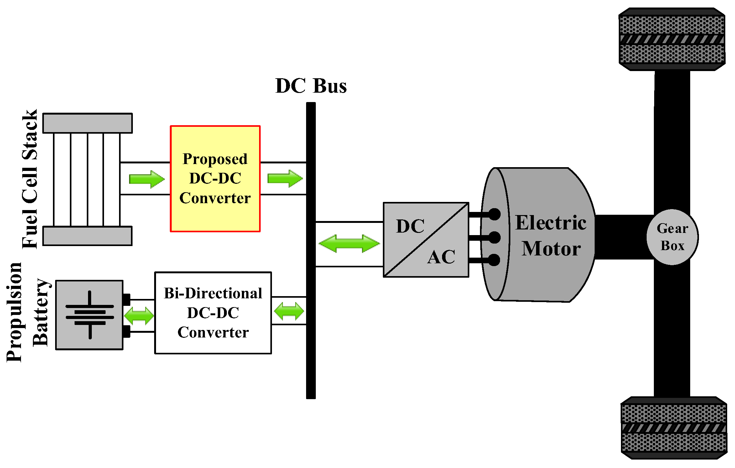
Due to the progressive depletion of conventional fossil fuel reserves and the deterioration of environmental quality, electrified transportation systems have attracted increasing interest. Fuel cells, recognized for their high efficiency and zero-emission characteristics, represent a promising energy source for electric vehicles [1,2]. However, their practical deployment is restricted by several inherent limitations. A single fuel cell generally provides a low output voltage of approximately 1.16 V, necessitating the series connection of many cells to obtain a usable voltage level, an arrangement that may compromise the long-term robustness and operational dependability of the stack [3,4]. Additionally, the output voltage of fuel cells fluctuates significantly with load variations due to their soft output characteristics [5]. Consequently, directly interfacing the fuel cell stack with a DC bus, which typically operates around 400 V in electric vehicle systems, is not feasible. To address this, a dc–dc converter with a high conversion ratio is therefore required to facilitate the connection between the fuel cell and the system’s DC bus [6], as depicted in Figure 1. Moreover, the converter must ensure minimal input-current ripple to prolong the fuel cell’s operational lifespan and incorporate the same ground to both input and output sides to mitigate electromagnetic interference (EMI) and enhance operational stability [7]. Isolated step-up DC–DC converters are capable of achieving high voltage gain primarily through an increase in the transformer turns ratio [8,9,10]. However, in applications such as electric vehicles, where system size and cost are critical considerations, non-isolated transformerless high-gain converters are often preferred. Their reduced hardware requirements and compact design make them more suitable as interface converters under such constraints. The conventional boost converter represents the most fundamental non-isolated topology [11]. While a sufficiently high duty cycle theoretically allows it to achieve large voltage gain, practical limitations such as parasitic effects restrict the achievable gain. Additionally, it is prone to extreme duty ratios, pronounced diode reverse-recovery losses, and hard-switching stress. These drawbacks make the conventional boost converter unsuitable for fuel cell applications.
To improve voltage gain, numerous boosting techniques have been explored [12]. One approach is the switched-inductor topology, as studied in [13,14]. The design in [13] provides a simple configuration with reduced input-current ripple, but the absence of a common ground between input and output can generate significant EMI issues. Conversely, the converter in [14] uses a shared ground but achieves only limited voltage gain. In [15], a switched-capacitor converter is proposed that doubles the output voltage and lowers voltage stress on diodes and capacitors; nevertheless, the switches operate under hard-switching, which constrains efficiency enhancement. Magnetically coupled structures provide another effective approach for boosting voltage, categorized into horizontal [16,17] and vertical [18,19] arrangements depending on the circuit layout. Coupled-inductor converters in [20,21] further enhance voltage gain without extreme duty cycles and enable soft-switching of main switches, though the soft-switching range is limited. In addition, these converters’ complex topologies increase overall size and cost.
For fuel cell vehicle applications, interface converters must exhibit minimal input-current ripple. By employing interleaved configurations, these converters effectively minimize input current variations and reduces current stress on switching elements by distributing the input current across multiple paths [22]. To enhance core utilization, a single coupled inductor with inverse [23] or direct [24] coupling can replace two separate inductors. Nevertheless, these designs still rely on hard switching for active switches. Auxiliary circuits are integrated in [25,26,27] to facilitate soft switching. In particular, the approach presented in [27] reduces the zero-crossing period of the current in the auxiliary circuit by connecting the auxiliary inductor to the primary inductor. However, despite this enhancement, the voltage step-up capacity of these converter designs is still inadequate to fulfill the operational demands of fuel cell systems.
The aforementioned non-isolated DC-DC converter topologies are incapable of simultaneously providing a high voltage conversion ratio, small input-current ripple, and complete soft-switching operation for all semiconductor devices. To address this limitation, this paper proposes a new interleaved converter that integrates the parallel-interleaved technique, flying-capacitor approach, switched-capacitor methodology, and ZVT cell. The proposed converter has the following advantages:
  • The main switches Sm1 and Sm2 turn on and off under ZVS, while the auxiliary switch turns on with ZCS and off with ZVS.
  • Main output diodes and auxiliary diodes turn off with ZCS, resulting in negligible reverse-recovery losses.
  • Voltage stress on all power semiconductors and capacitors is limited to half of the output voltage, reducing switching and conduction losses and improving efficiency and reliability.
  • Input-current ripple is minimized through interleaving of two inductors, lowering stress on the fuel cell and enhancing efficiency.
  • The converter shares a common ground between input and output, reducing EMI and simplifying system integration.
By combining these advantages in one compact topology, the converter offers an effective alternative to conventional designs that typically compromise between gain, efficiency, and switching performance. The structure of this paper is as follows: Section 2 details the circuit configuration and operational principles of the proposed converter. Section 3 provides a comprehensive analysis of the converter’s characteristics. Subsequently, Section 4 outlines the parameter design methodology and discusses the experimental results. Finally, the conclusion is summarized in Section 5.

2. Operating Principle of the Converter

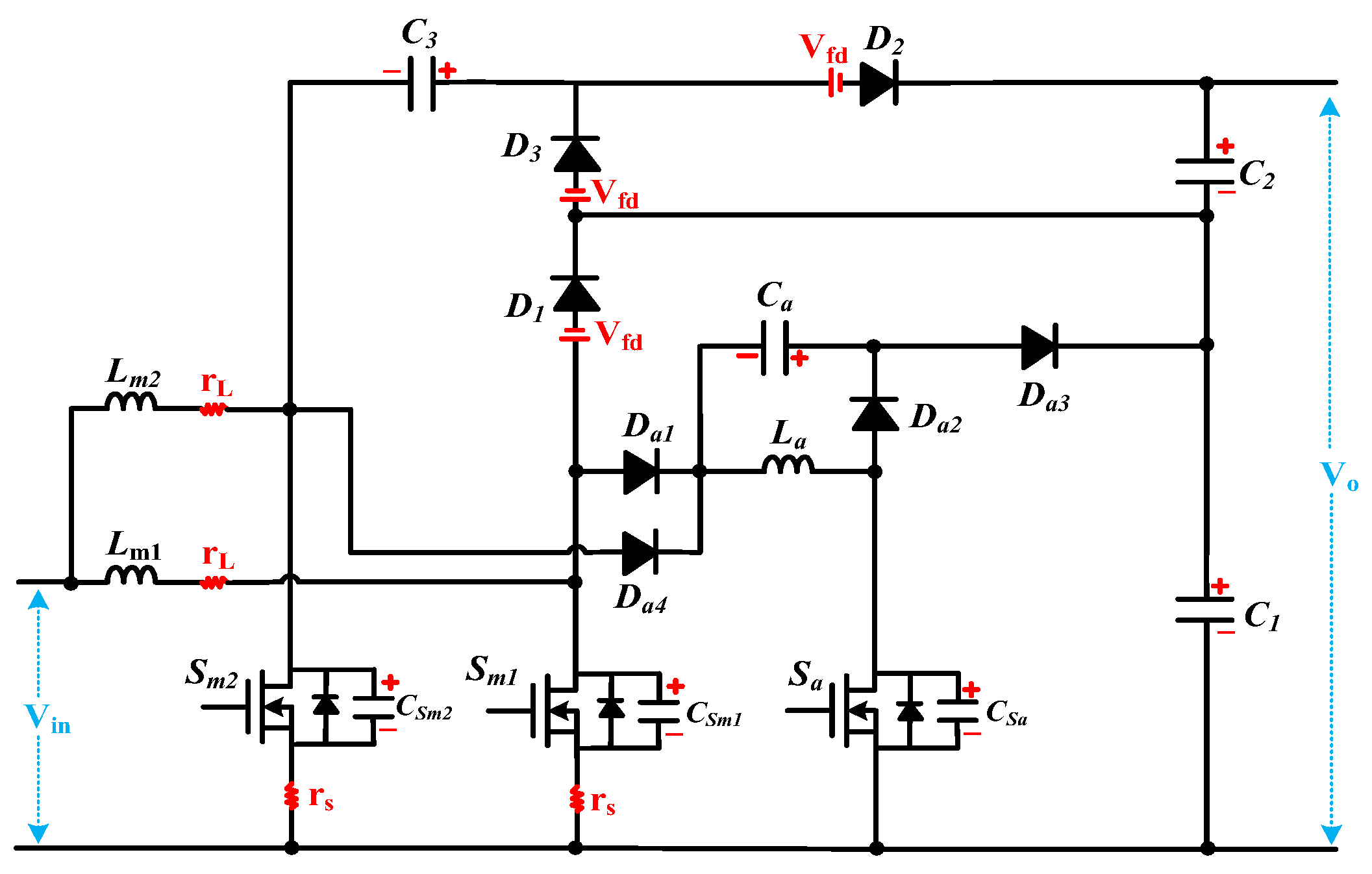
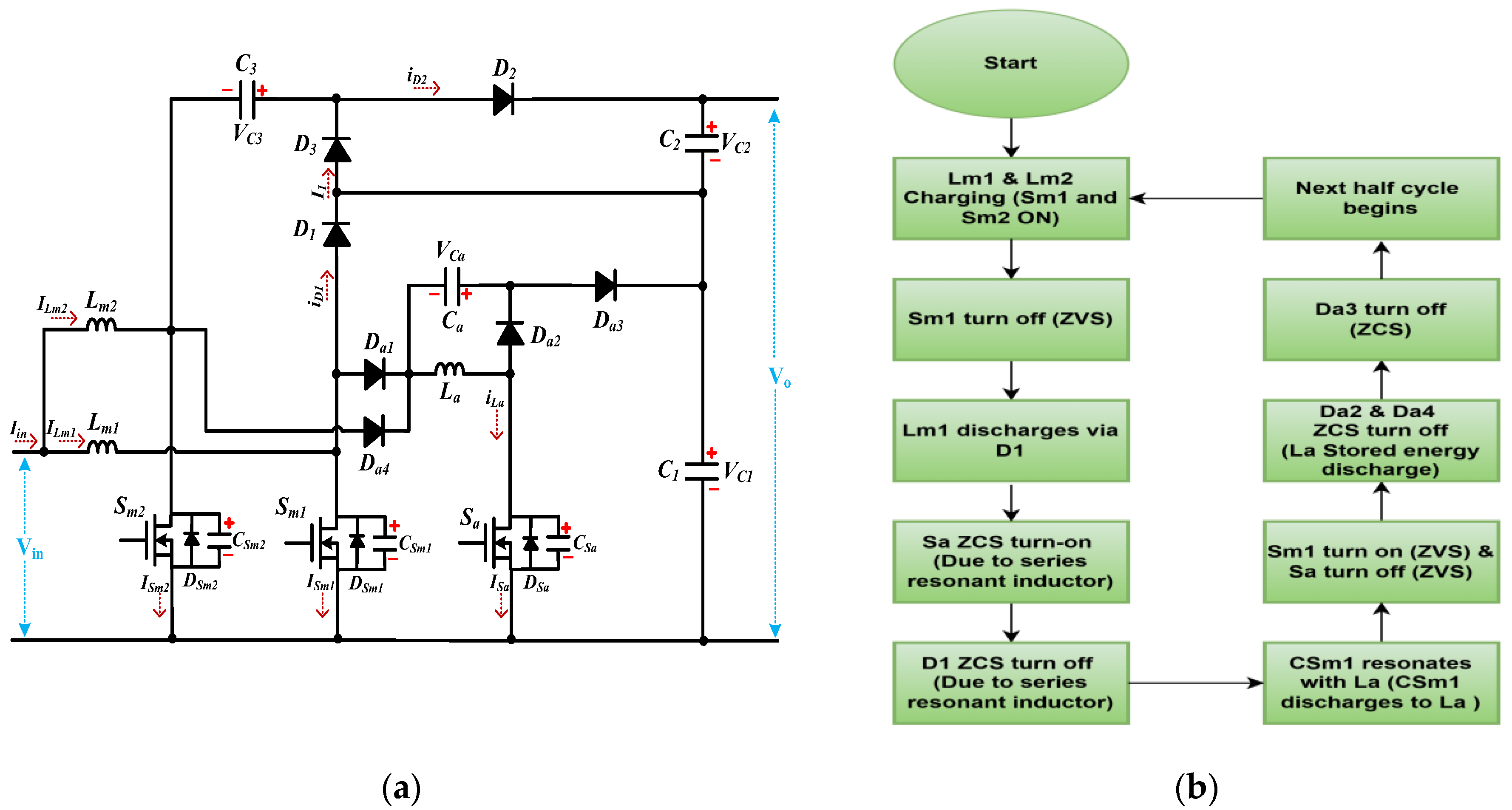
Figure 2a illustrates the circuit configuration of the proposed converter. The converter is composed of a two-phase interleaved boost converter, where one cell is made up of Lm1, Sm1, D1, and C1, and the second cell includes Lm2, Sm2, D2, and C2. It also features a diode-capacitor network formed by D3 and C3, along with a single auxiliary soft-switching circuit that consists of the auxiliary switch Sa, auxiliary inductor La, auxiliary capacitor Ca, and auxiliary diodes Da1, Da2, Da3, and Da4. The two boost converter stages are configured in an input-parallel and output-series (IPOS) arrangement, facilitating a reduction in input-current ripple while enhancing the output voltage gain.
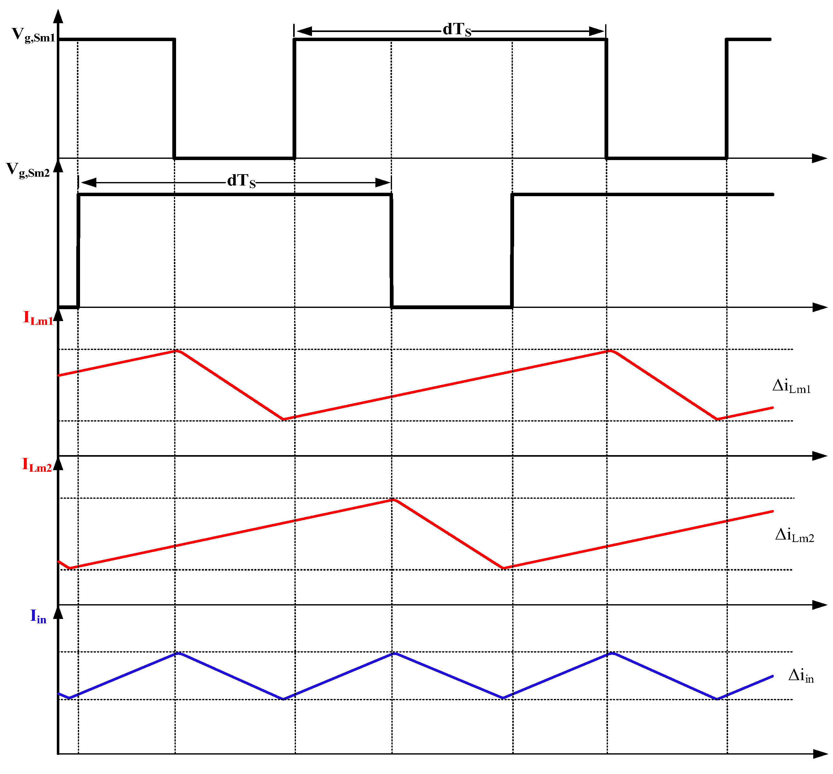
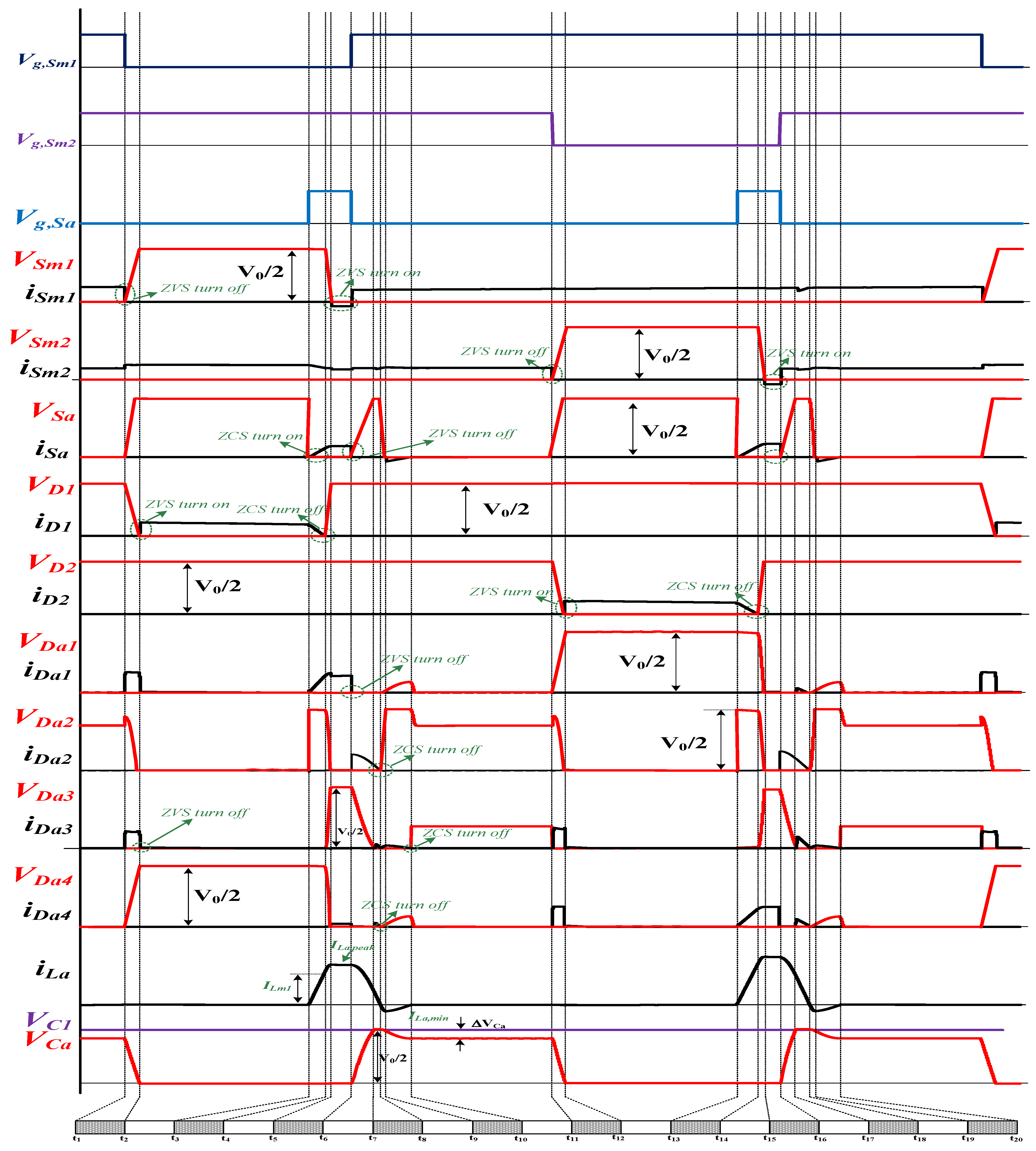
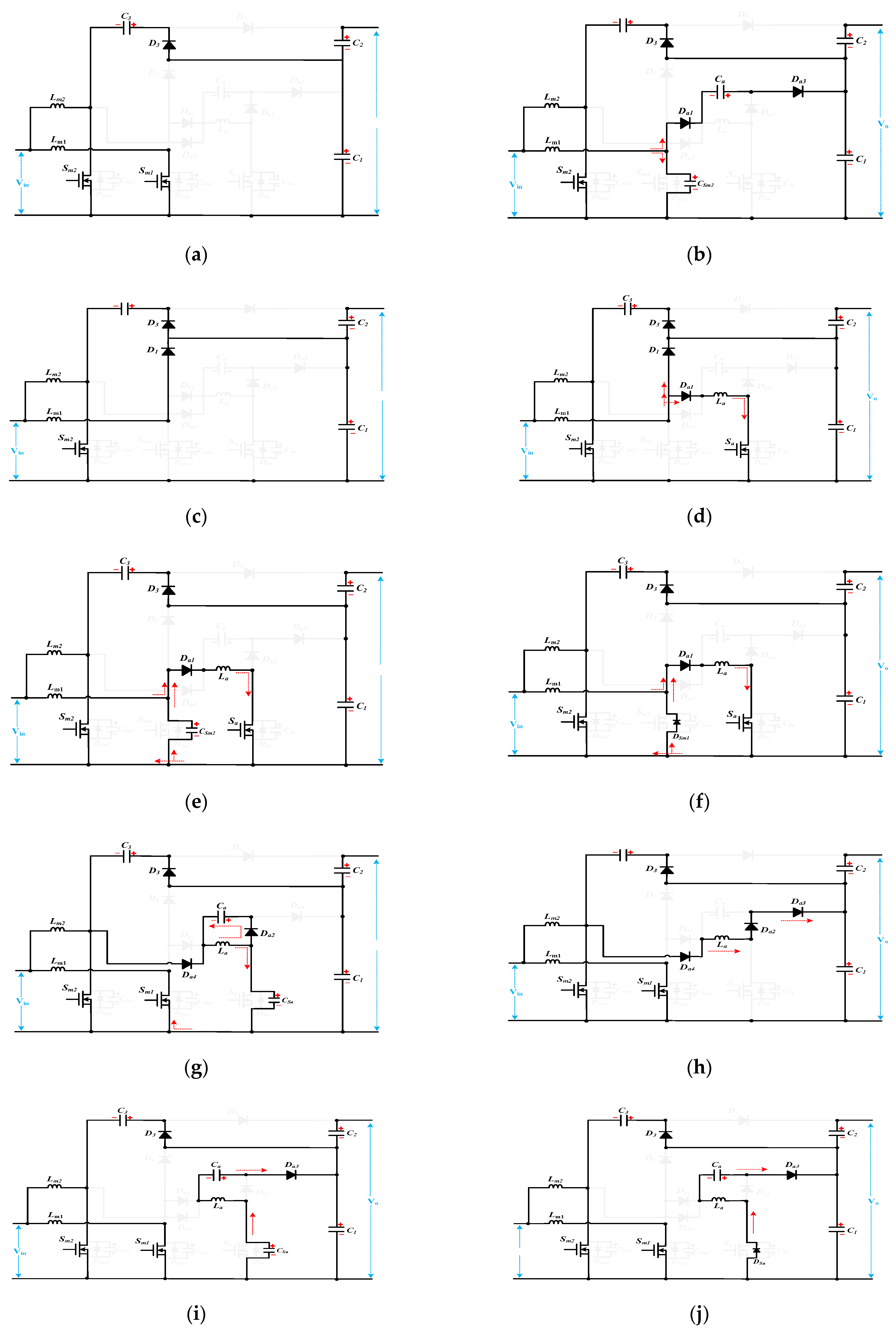
Typically, the operating behavior of a two-phase interleaved boost converter can be classified into two conditions: when the duty cycle is greater than or less than 0.5. In this study, the focus is solely on the case where the duty cycle is greater than 0.5, as it sufficiently meets the voltage gain requirements of the target application. In this operating mode, the converter undergoes 20 different intervals within a single switching cycle. Owing to the symmetry of the interleaved structure, only the ten stages associated with switch Sm1 are examined, as the behavior of the complementary phase is identical. A simplified operational flowchart of the proposed converter is shown in Figure 2b to provide a clear overview of the overall system operation. The corresponding key waveforms, obtained from MATLAB R2024b/Simulink simulations, and the equivalent circuit for each stage are presented in Figure 3 and Figure 4, respectively. The description of each operating stage is provided as follows.
Stage 1 [Before Turn−Off of the Main Switch Sm1, Figure 4a]: During this interval, iSm1 = ILm1, iSm2 = ILm2 + I1, iSa = 0, iLa = 0, iD1 = 0, iD2 = 0, iD3 = I1 and VCa = 0. Before the instant t1, the interleaved boost converter operates in its normal on−state interval with a duty ratio greater than 0.5. In this interval, both main switches and diode D3 are conducting, while the auxiliary switch and main diodes D1 and D2 remain in the off state. During this mode, the input inductors Lm1 and Lm2 are energized by the input source Vin, thus
L m 1 d i L m 1 d t = L m 2 d i L m 2 d t = V i n
Since capacitors C1 and C3 are charged in parallel, the voltage difference between them remains small, though it cannot be neglected. This slight voltage imbalance gives rise to a current through diode D3, denoted as I1. Under this condition, the current through switch Sm1 corresponds to the inductor current Lm1, while the current through switch Sm2 is the sum of iLm2 and I1. This stage ends when the main switch Sm1 turns off at time t = t1.
Stage 2 [t1 < t < t2, Figure 4b]: At t = t1, auxiliary diodes Da1 and Da3 become forward biased and start conducting. During this interval, the main inductor current ILm1 discharges the auxiliary capacitor Ca, while the output capacitance of main switch CSm1 is simultaneously charged. Because Ca has a significantly higher capacitance compared to CSm1, the main switch Sm1 achieves turn−off under ZVS condition. The voltage equations of the circuit elements in this interval are described as follows:
V C a ( t ) = I L m 1 C a + C S m 1 ( t t 1 )
V S m 1 = V C 1 V C a t
The parasitic capacitor CSm1 charges up to the voltage VC1 while the capacitor Ca discharges completely to zero at t = t2. At this moment, the auxiliary diodes Da1 and Da3 turn off with ZVS and this stage ends. The time span of this interval is obtained as follows:
t 2 t 1 = C a V C 1 I L m 1
Stage 3 [t2 < t < t3, Figure 4c]: Before this interval, iSm1 = 0, iSm2 = ILm2 + I1, iSa = iLa = 0, iD1 = 0, iD2 = 0, iD3= I1 and VCa = 0 are valid. At instant t2, the main diode D1 switches on, directing the input current toward the load. This stage concludes at t3, when the auxiliary switch Sa begins to turn on. During this stage, the input voltage Vin charges Lm2 and Lm1 together with Vin supplies energy to C1 and C3. So, for this stage, the equations
L m 1 d i L m 1 d t = V i n V C 1
L m 2 d i L m 2 d t = V i n
are valid.
Stage 4 [t3 < t < t4, Figure 4d]: Before this interval, iSm1 = 0, iSm2 = ILm2 + I1, iSa = iLa = 0, iD1 = ILm1, iD2 = 0, iD3 = I1 and VCa = 0 are valid. At t3, auxiliary switch Sa turns on. As a result, the current iLa begin to rise linearly, with the rate of increase governed by the slope given below:
d i L a d t = V C 1 L a
This effectively redirects the current flow away from the primary diode D1. Thus, the auxiliary switch Sa activates with ZCS condition at t4, while the main diode D1 deactivates under ZCS at t4. This occurs because of the series arrangement between the auxiliary switch Sa and the inductor La. The interval concludes at t4, when current iLa equals the input current ILm1 and the current iD1 reaches zero. The duration of this interval can be calculated using (7) as follows:
t 01 = I L m 1 V C 1 L a = P o V i n V C 1 L a
Stage 5 [t4 < t < t5, Figure 4e]: At moment t4, the main diode D1 is turned off. Subsequently, resonance begins between La and CSm1, transferring the entire stored energy in CSm1 to La. This mode concludes once CSm1’s voltage drops to zero and the current through the auxiliary inductor La reaches its peak value, ILa,peak.
i L a ( t ) = I L m 1 + V C 1 Z 1 sin ω 1 ( t t 4 ) ,         t 4 < t < t 5
V C S m 1 ( t ) = V C 1 cos ω 1 ( t t 4 ) ,         t 4 < t < t 5
In Equations (9) and (10),
Z 1 = L a C S m 1
ω 1 = 1 L a C S m 1
ILa,peak can be determined from Equation (9) at time t = t5 by
I L a , peak = I L m 1 + V C 1 Z 1
The duration of this operating interval is obtained from the following relation:
t 02 = π 2 ω 1 = π 2 L a C S m 1
Stage 6 [t5 < t < t6, Figure 4f]: At t = t5, once VCSm1 reaches zero, the body diode DSm1 of the switch Sm1 is activated. This clamps the voltage across Sm1 and La to zero and holds the current iLa constant at ILa,peak. This allows switch Sm1 to be turned on with ZVS condition. The mathematical relations describing this interval are given by the following:
I D S m 1 = I L a , peak I L m 1
Stage 7 [t6 < t < t7, Figure 4g]: At the start of this interval, iSm1 = 0, iSm2 = ILm2 + I1, iSa = iLa = ILa,peak, iD1 = 0, iD2 = 0, iD3 = I1 and VCa = 0 are valid. At moment t = t6, the auxiliary diode Da1 turn off with ZVS, the main switch Sm1 receives a turn-on gate signal, and the auxiliary switch Sa has its gate signal removed at the same instant. As a result, Sm1 achieves ZVS turn-on, while Sa undergoes ZVS turn-off via capacitor Ca. Once Sa is switched off, conduction transfers to diode Da2, which turns on with ZVS, and subsequently, La engages in a resonant interaction with Ca and CSa. The governing equations for this resonant interval can be derived as follows:
i L a ( t ) = I L a , peak cos ω 2 ( t t 6 ) ,         t 6 < t < t 7
V C S a ( t ) = V C a ( t ) = I L a , peak Z 2 ( t ) sin ω 2 ( t t 6 ) ,         t 6 < t < t 7
In Equations (16) and (17),
Z 2 = L a C S a + C a
ω 2 = 1 L a C S a + C a
The length of this resonance interval is determined using the following expression:
t 7 t 6 = L a C a + C S a sin 1 V C 1 I L a , peak L a C a + C S a
The auxiliary switch’s turn off voltage is predominantly influenced by Ca and La because CSa is significantly smaller than Ca. This interval terminates at t = t7, when VCa and VCSa rise to VC1, resulting in the forward conduction of diode Da3.
Stage 8 [t7 < t < t8, Figure 4h]: Once VCa reaches VC1, diode Da3 conducts, transferring the remaining energy stored in the auxiliary inductor La to the output. This interval concludes at t = t8, when the current iLa falls to zero, resulting in the ZCS turn-off of diodes Da2 and Da4.
Stage 9 [t8 < t < t9, Figure 4i]: At t = t8, CSa and La enter a resonant interaction. Since Ca is much larger than CSa, VCa is therefore assumed constant throughout this resonant interval. Consequently, the voltages and currents equations of the elements involved in the resonant process can be analytically determined as follows:
i L a ( t ) = V C 1 Z 3 sin ω 3 ( t t 8 ) ,         t 8 < t < t 9
V C S a ( t ) = V C 1 cos ω 3 ( t t 8 ) ,         t 8 < t < t 9
In Equations (21) and (22),
Z 3 = C S a L a
ω 3 = 1 L a C S a
This resonant mode ends once VSa reaches zero and the inductor current iLa attains its minimum ILa,min which can be determined from Equation (21) as follows:
I L a , min = V C 2 Z 3
The length of this mode is computed as
t 9 t 8 = π 2 L a C S a
Stage 10 [t9 < t < t10, Figure 4j]: At t9, the anti-parallel diode of auxiliary switch DSa becomes forward-biased, initiating a resonant process between La and Ca. The current and voltage equations for this resonant interval can be found as follows:
i L a ( t ) = I L a , min cos ω 4 ( t t 9 ) ,         t 9 < t < t 10
V C S a ( t ) = V C 1 + I L a , min Z 4 ( t ) sin ω 4 ( t t 9 ) ,         t 9 < t < t 10
In Equations (27) and (28),
Z 4 = L a C a
ω 4 = 1 L a C a
The interval terminates once iLa falls to zero, and its duration can be determined from the following expression:
t 10 t 9 = π 2 L a C a
The voltage variation ∆VCa across Ca during this interval can be evaluated from Equations (25), (28) and (31) as follows:
Δ V C a = V C 1 C S a C a
Upon completion of this interval, the first segment of the switching cycle, which characterizes the conduction and switching of Sm1, concludes. The subsequent segment, associated with Sm2, occurs next, following the same operational pattern to maintain interleaved symmetry.

3. Analysis of the Converter Characteristics

The detailed analysis of the proposed converter is as follows.

3.1. Voltage Gain

3.1.1. Ideal Voltage Gain of the Proposed Converter

For the proposed converter, the auxiliary circuit has a small impact on the voltage gain. Therefore, for simplification of the derivation, the auxiliary circuit can be disregarded. It is assumed that all circuit elements are ideal and the capacitance and inductance values are sufficiently large so that the voltage across each capacitor remains essentially constant. Figure 4c indicates that Sm2 is switched on while diode D3 is conducting. Under this condition, C1 and C3 are linked in parallel, so the voltage on each capacitor becomes the same. In CCM operation, the converter’s voltage gain is derived by applying the volt-second balance principle to the input inductors Lm1 and Lm2.
V i n d + V i n V C 1 1 d = 0
V i n d + V i n + V C 1 V o 1 d = 0
also
V C 1 = V C 3
Within a single switching period, the converter’s output voltage can be expressed as follows:
V C 1 + V C 2 = V o
where Vin and Vo refer to the input and output voltages, while VC1, VC2, and VC3 correspond to the voltages across C1, C2, and C3. Thus,
V o = 2 V i n 1 d V C 1 = V C 2 = V C 3 = V i n 1 d
using Equation (37), the voltage gain G is given by
G = 2 1 d

3.1.2. Non-Ideal Voltage Gain of the Proposed Converter

In order to evaluate the voltage gain considering parasitic components, the parasitic elements are defined as follows: rS is the MOSFET on-resistance and the corresponding conduction voltage drop is modeled as VS, Vfd is the diode forward conduction voltage drop, rL is the equivalent series resistance (ESR) of the input inductors, and the ripple current in the inductors is neglected. The configuration of the proposed converter, along with its parasitic components, is shown in Figure 5. Just like the ideal case, the influence of the ZVT cell on the voltage gain is small and can thus be ignored. Using the volt-second balance principle for inductors Lm1 and Lm2, and the ampere-second balance principle for capacitors C1–C3 in CCM, the following expressions can be obtained:
d T s ( V i n I L m 1 r L V S ) + ( 1 d ) T s ( V i n I L m 1 r L V f d V C 1 ) = 0 [ d T s ( V i n I L m 2 r L V S ) + ( 1 d ) T s ( V i n I L m 2 r L V C 2 V S 2 V f d ) = 0
I L m 2 V o R T s ( 1 d ) + V o R d T s = 0 I D 2 T s = I L m 2 ( 1 d ) T s
During the switching period, the output voltage of the converter is always described by
V o = V C 1 + V C 2
According to Equations (39)–(41) the volage gain G and the capacitor voltages could be derived by
G = V o V i n = 2 ( 1 + d ) V S + 3 ( 1 d ) V f d V i n 1 d + 2 r L R ( 1 d )
The capacitor voltages are calculated by
V C 1 = V i n I L 1 r L d V S ( 1 d ) V f d 1 d
V C 2 = V i n I L 2 r L V S 1 d 2 V f d
V C 3 = V i n I L 1 r L V S 2 ( 1 d ) V f d 1 d

3.2. Voltage and Current Stress Across the Semiconductor Devices

The operating principles indicate that C1, C2 and C3 sustain identical voltages, each equal to half of the output voltage, i.e., Vo/2. The main switch Sm1 and auxiliary switch Sa experience voltage stresses equal to VC1, while the main switch Sm2 is subjected to a voltage stress of V0 − VC3. The diodes D1, D2, and D3 are stressed by voltages of VC1, Vo −VC3, and VC2, respectively. Accordingly, the capacitor and device voltages are expressed as
V C 1 = V C 2 = V C 3 = V C a = V o 2 V S m 1 = V S m 2 = V S a = V o 2 V D 1 = V D 2 = V D 3 = V o 2 V D a 1 = V D a 2 = V D a 3 = V D a 4 = V o 2
As all switches experience a voltage stress of Vo/2, devices with low conduction resistance may be utilized to effectively reduce conduction losses and thereby improve the overall efficiency. In addition, the voltage stresses across the capacitors are restricted to 50% of the output voltage, contributing to smaller component sizes, minimized risk of failure, and enhanced system reliability.
Based on the steady-state operation under CCM and the waveforms shown in Figure 3 along with the equivalent circuits in Figure 4, the average currents of the main switches and diodes are derived as follows:
I S m 1 , a v g = d 1 d × V o R I S m 2 , a v g = 1 1 d × V o R I D 1 , a v g = I D 2 , a v g = I D 3 , a v g = V o R
Similarly, the average currents of the auxiliary switches and diodes are derived as follows:
I S a , a v g = I L a , p e a k t S a T s I D a 1 , a v g = 1 T s V C 1 C a + 1 2 I L a , p e a k t S a I D a 2 , a v g = 1 T s V C 1 ( C a + C S a ) + L a I L a , p e a k 2 V C 1 I D a 3 , a v g = 1 T s V C 1 C a C S a + L a I L a , p e a k 2 V C 1 I D a 4 , a v g = 1 T s V C 1 ( 2 C a + C S a ) + 1 2 I L a , p e a k t S a + L a I 7 2 2 V C 1
The RMS currents of the main switches and diodes are given as follows:
I S m 1 , r m s = d 1 d × V o R I S m 2 , r m s = 1 d ( 1 d ) × V o R I D 1 , r m s = I D 3 , r m s = 1 1 d × V o R I D 2 , r m s = 1 d × V o R
Similarly, the RMS currents of the auxiliary switches and diodes are given as follows:
I S a , r m s = I L a , p e a k 2 t S a 3 T s I D a 1 , r m s = I L m 1 C a V C 1 + I L a , p e a k 2 t S a 3 T s I D a 2 , r m s = I L a , p e a k 2 [ ( t 7 t 6 ) + ( t 8 t 7 ) ] 3 T s I D a 3 , r m s = 2 I L m 1 C a V C 1 + 2 3 I 7 2 t 78 T s I D a 4 , r m s = I L m 1 C a V C 1 + I L a , p e a k 2 t S a 3 + I 7 2 t 8 t 7 3 T s

3.3. Ripple Analysis

Over a single switching period, switches Sm1 and Sm2 share the same duty cycle while being phase-shifted by 180°. This phase arrangement effectively minimizes the ripple in the input current.
Using Equation (40), the average values of the inductor currents ILm1 and ILm2 are determined, and their final forms are shown in Equation (51):
I L m 1 = I L m 2 = V o R 1 d
I i n = I L m 1 + I L m 2 = 2 V o R 1 d
In the switching interval when Sm1 is turned on, the inductor Lm1 is directly connected to the input source and its current increases linearly. Similarly, when Sm2 is turned on, the inductor Lm2 experiences the input voltage and its current rises with the same linear slope. Based on these charging intervals, the current ripples of Lm1 and Lm2 can be expressed as follows:
Δ i L m 1 = Δ i L m 2 = d V i n L f s
where fs represents the switching frequency of the power switches. For d > 0.5, the two inductor currents overlap for (2d − 1)Ts.
The input current slope is
Δ i L m 1 = Δ i L m 2 = d V i n L f s
Hence, the input current is
Δ i i n = V i n L ( 2 d 1 ) T s = V i n 2 d 1 L f s
And the ripple rates rL1 and rL2 of inductors Lm1 and Lm2 can also be found as
r L 1 = r L 2 = d ( 1 d ) 2 R 2 L f s
A slight increase in input-current ripple may occur if the two interleaved input inductors have different values, due to differences in their charging and discharging rates. In an interleaved converter, the total input current is the sum of the phase currents, so any imbalance reduces the natural ripple-cancelation effect. As shown in Figure 6, the input-current ripple is minimal when the inductors are equal, slightly higher for small differences, and largest for significant mismatches. This behavior is typical in all interleaved converters. Importantly, these variations do not affect the proposed converter’s soft-switching operation, voltage gain, or voltage stress, which are determined by the topology and duty cycle rather than the exact inductor values.

3.4. Comparisons with Other Converters

A comparison between the proposed converter and the closely related interleaved converters from recent literature is presented in Table 1.
The converters in [28,29] achieve the same voltage gain and offer reduced input-current ripple. Nevertheless, in comparison with the proposed converter, the converter in [33] experiences relatively high voltage stress on two diodes and one capacitor, equal to the output voltage. Furthermore, the design in [29] lacks a common ground, which can introduce EMI concerns. In addition, in both converters, the power switches operate under hard-switching conditions, leading to increased switching losses and reduced efficiency. In [30], a converter employing a three-winding coupled inductor is proposed. Its advantages include small input-current ripple, high step-up ratio, and reduced voltage stress on the diodes. Nevertheless, the switching devices operate under hard-switching conditions. Furthermore, every switch experiences a voltage stress identical to the output voltage. In [31], a single-switch converter based on a coupled inductor is proposed to achieve ultra-high voltage gain. Although this configuration reduces the voltage stresses on both the semiconductor switches and diodes, the improvement in efficiency is limited by the hard-switching operation of the semiconductor switches and the reverse-recovery characteristics of the diodes. Moreover, the high input-current ripple limits its suitability for fuel cell vehicle applications. In [32], a converter employing an improved Dickson-based charge-pump voltage multiplier at the output is introduced to achieve high voltage gain and reduce switch voltage stress. However, the semiconductor devices still experience hard-switching losses, reducing efficiency, and the complex circuit structure increases both the converter’s volume and cost. The interleaved converter in [33] incorporates auxiliary circuits in each phase to achieve complete soft-switching operation. However, the resulting voltage gain is insufficient to effectively connect the fuel cell with the DC power system. In addition, the converter in [33] requires twice as many auxiliary circuits as the proposed design. Coupled-inductor-based interleaved structures are proposed in [34,35,36], which are capable of achieving both low input-current ripple and high voltage gain simultaneously. Moreover, by incorporating an active clamp circuit, the main switches operate under soft-switching conditions. Nevertheless, the soft-switching capability in [34,35] is restricted to an arrow range, and the non-common ground between the input and output in [35,36] introduces considerable EMI concerns. In addition, their circuit structures are more complex than those of the proposed converter, leading to increased volume and cost. Although the CI-based converter proposed in [37] has a low number of components as compared to the proposed converter, the turn-off of the main switches is hard-switched which reduces overall efficiency. From the above comparisons, it can be concluded that the proposed converter offers superior performance, characterized by reduced input-current ripple, high step-up ratio with reduced component stress, wide-range soft-switching capability for all active devices, and a common-ground structure.

4. Parameter Design and Experimental Results

In this section, the design considerations of the proposed converter are presented. The proposed interleaved boost converter is configured to operate in continuous conduction mode (CCM), while ensuring both ZVS and ZCS conditions.

4.1. Selection of the Boost Inductors Lm1 and Lm2

The inductor design is influenced by the allowable current ripple rates rLm1 and rLm2, the nominal input and output voltages Vin and Vo, the rated load resistance, and the operating switching frequency fs:
L m 1 = L m 2 = d ( 1 d ) 2 × R 2 f s r
The proposed converter typically operates with a duty cycle between 0.5 and 0.75. At a 0.5 duty cycle, the design requires the maximum inductance values. At this point, to keep the inductor currents continuous, both inductor current ripple ratios rLm1 and rLm2 are set to 70%.
L m 1 = L m 2 = 0.5 × ( 1 0.5 ) 2 × 160 2 × 50000 × 0.7 = 285 μ H
To ensure the inductor current ripple remains small during light-load operation, and to provide additional margin, the inductance is set to 330 μH.

4.2. Capacitor Design

When selecting the output capacitors, the output-voltage ripple must be carefully considered. Although larger capacitors help to minimize this ripple, they also increase the converter’s overall cost and physical size. Thus, an appropriate trade-off between capacitance and cost must be achieved. Given that capacitors C1 and C2 govern the output-voltage ripple in the proposed converter, the corresponding output-voltage ripple Δuo can be formulated as
Δ V o = Δ V C 1 + Δ V C 2
where ∆V1 and ∆V2 are the voltage ripples across C1 and C2, respectively. To facilitate maintenance and simplify the analysis, the capacitors are selected to have equal values, i.e., C1 = C2 = C3 = C. Consider the sub-interval where Sm1 ON and Sm2 is off; D2 conducts while D1 and D3 blocks. In this interval, Lm1 is charged from the input with a linearly increasing current, while the input source together with Lm2 and C3 transfer energy to C1, C2, and the load, so ILm2 decreases. The currents through C1 and C2 point toward their positive plates (charging), which drives a roughly linear rise in the output voltage during this sub-interval. Therefore, the output-voltage ripple over one switching period can be computed from the linear capacitor charge in this sub-interval, leading to Equation (60).
Δ V o = 2 d 2 V o R f C 1 d
Considering that the proposed converter is connected in series with the inverter, the allowable ripple of the output voltage is restricted to ±0.15% of the rated output voltage in order to meet load requirements. The capacitor sizing is then determined using Equation (61) as follows:
C = 2 d 2 V o ( 1 d ) f R Δ V o = 375 μ F
Finally, to prevent excessive output-voltage ripple under heavy-load conditions and to provide an adequate design margin, a capacitor value of 450 μF is selected.

4.3. Condition of Soft Switching

The resonant capacitors CSm1 and CSm2 are the parasitic capacitances of the main switches Sm1 and Sm2, respectively. In contrast, the resonant capacitor Ca and the resonant inductor La are additionally added components introduced into the circuit to form the resonant network. To ensure ZVS during the turn-on transition of the main switches, the auxiliary switch Sa must satisfy the following condition at its turn-on time:
t S a t 01 + t 02
where tSa denotes the turn-on time of the auxiliary switch, t01 represents the current rise time of the auxiliary inductor La during Mode 1, and t02 is the resonant transition time in Mode 2. The selection of tSa is critical and must satisfy two primary constraints. First, to significantly reduce the reverse-recovery losses of the main diodes, i.e., D1 and D2, the current rise time of the auxiliary inductor during Mode 1 should be larger than three times the diode’s reverse-recovery time trr. Considering Mode 2’s resonant interval t02, tsa is chosen to be five times greater than trr. Second, to minimize conduction losses and maintain a compact auxiliary circuit, tSa should be chosen to be less than one-tenth of the switching period Ts. Therefore, tsa is constrained by
5 t r r t S s 1 10 T s
The main diode generally has a reverse-recovery time of several tens of nanoseconds. Thus, considering the chosen switching frequency and Equation (63), tSa ≤ 2 μs is determined. If tsa is chosen too small, the inductance of the auxiliary inductor becomes insufficient to support proper resonant operation, causing the main switch to fail to achieve ZVS turn-on at light load. Conversely, if tSa is too large, the conduction losses in the auxiliary components increase significantly. Hence, tSa = 1000 ns is selected.

4.4. Auxiliary Inductor Design

The auxiliary inductor La governs the current change rate di/dt in the auxiliary switch at the moment of turn-on. Based on Equations (8), (14) and (62), the required value of La is selected as
L a π 2 C S m 1 + π 2 4 C S m 1 + 4 P o V i V o t S a 2 P o V i V o 2
Based on the design parameters, the maximum value of the auxiliary inductor obtained from (64) is La ≤ 16.96 μH. To reduce the freewheeling interval and associated conduction losses, La should be chosen below this upper limit. Therefore, in this work, La = 10 μH is selected.

4.5. Auxiliary Capacitor Design

The auxiliary capacitor Ca provides dv/dt for auxiliary switch Sa during turn-off. For the main switch to realize ZVS turn-off, the voltage across the auxiliary capacitor must reach the voltage across C1 at the end of stage 7. Since the auxiliary inductor supplies the required charging energy to the auxiliary capacitor, the capacitance value is determined according to Equation (65).
C a < L a I L a , peak V o 2
From Equation (65), the value of auxiliary capacitance Ca is obtained as Ca ≤ 10 nF. To improve the ZVS turn-off range when the converter operates at light load, Ca needs to be chosen as small as possible to the maximum value. Accordingly, a capacitance of 3.3 nF is chosen in this work.

4.6. Experimental Results

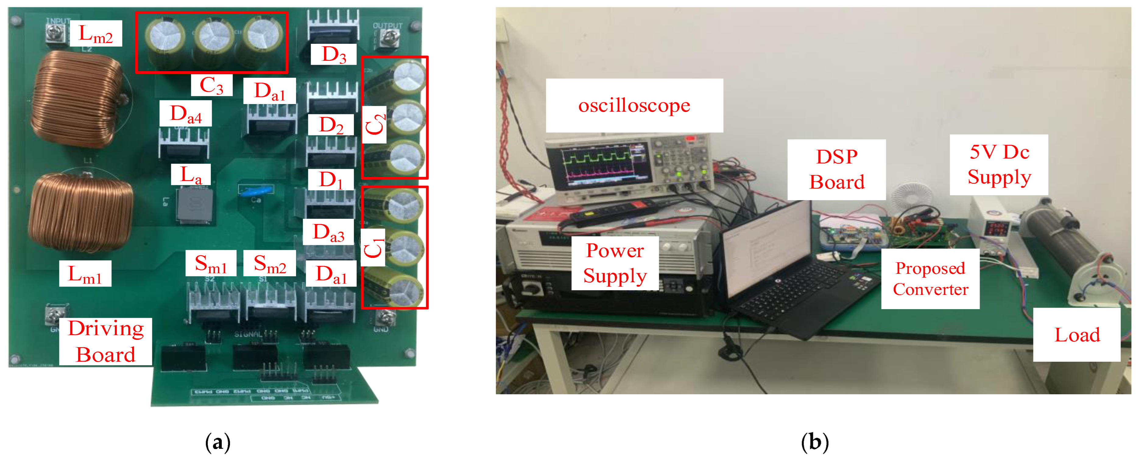
To validate the theoretical analysis of the proposed converter, an experimental prototype with a 1 kW rating was constructed. The details of parameters used in the experiment are outlined in Table 2, and resistive load is employed during the measurements. Figure 7a depicts a photograph of the developed dc–dc converter used in the laboratory setup, while Figure 7b illustrates the experimental test arrangement.
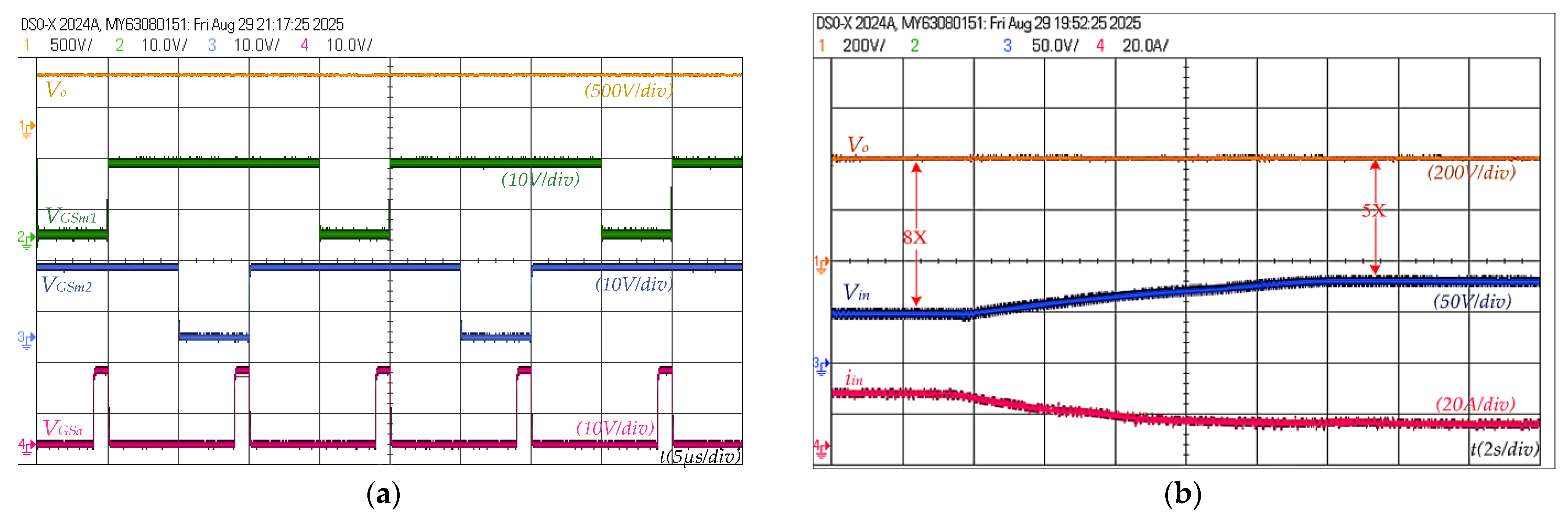
The KEYSIGHT InfiniiVision MSOx2024A oscilloscope (Keysight Technologies, Santa Rosa, CA, USA) is employed to measure the current and voltage waveforms. A digital signal processor (DSP) platform based on the TMS320F28335 is employed to generate PWM gate signals for the MOSFETs in the experimental setup. The ePWM module is utilized to produce gate pulses with complementary duty ratios. The gate signal profiles, along with the measured output-voltage waveform corresponding to a 50 V input condition, are presented in Figure 8a. As shown in Figure 8a, the output voltage reaches 400 V, corresponding to a voltage-gain factor of 8. These results indicate that the proposed converter architecture supports high step-up voltage conversion capability.
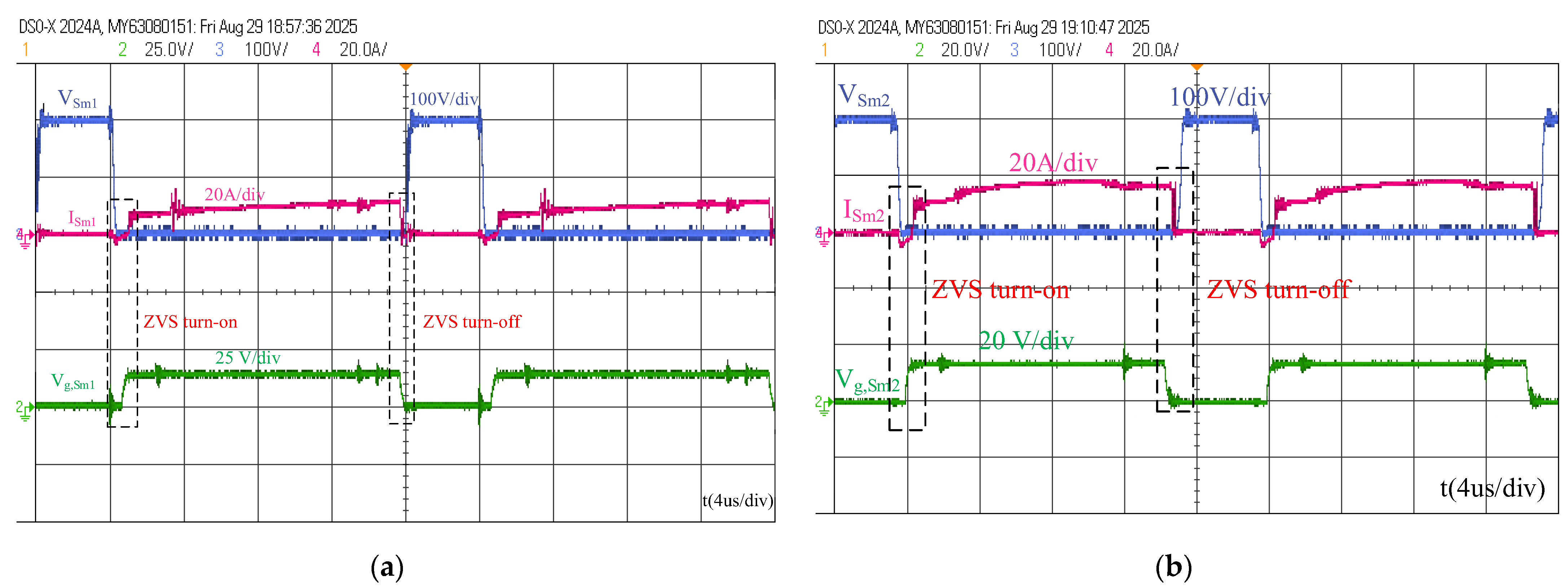
The experimental results for the soft switching of main switches Sm1 and Sm2 are depicted in Figure 9a,b. As illustrated in Figure 9a, the control signal of the main switch Sm1, its drain–source voltage VSm1, and drain current iSm1 are compared. Similarly, Figure 9b presents the corresponding waveforms for Sm2. It can be observed that the drain to source voltages of the main switches Sm1 and Sm2 reduce to zero prior to the application of the turn-on signal, confirming that each switch operates under ZVS at turn-on. Furthermore, the main switches also turn off under ZVS conditions, confirming the effectiveness of the proposed auxiliary circuit. Consequently, the two main switches in the dual branches achieve full ZVS during both switching intervals with the support of a single auxiliary network. Moreover, the voltage stress of each active switch remains limited to approximately one-half of the output voltage (200 V), which agrees with Equation (46).
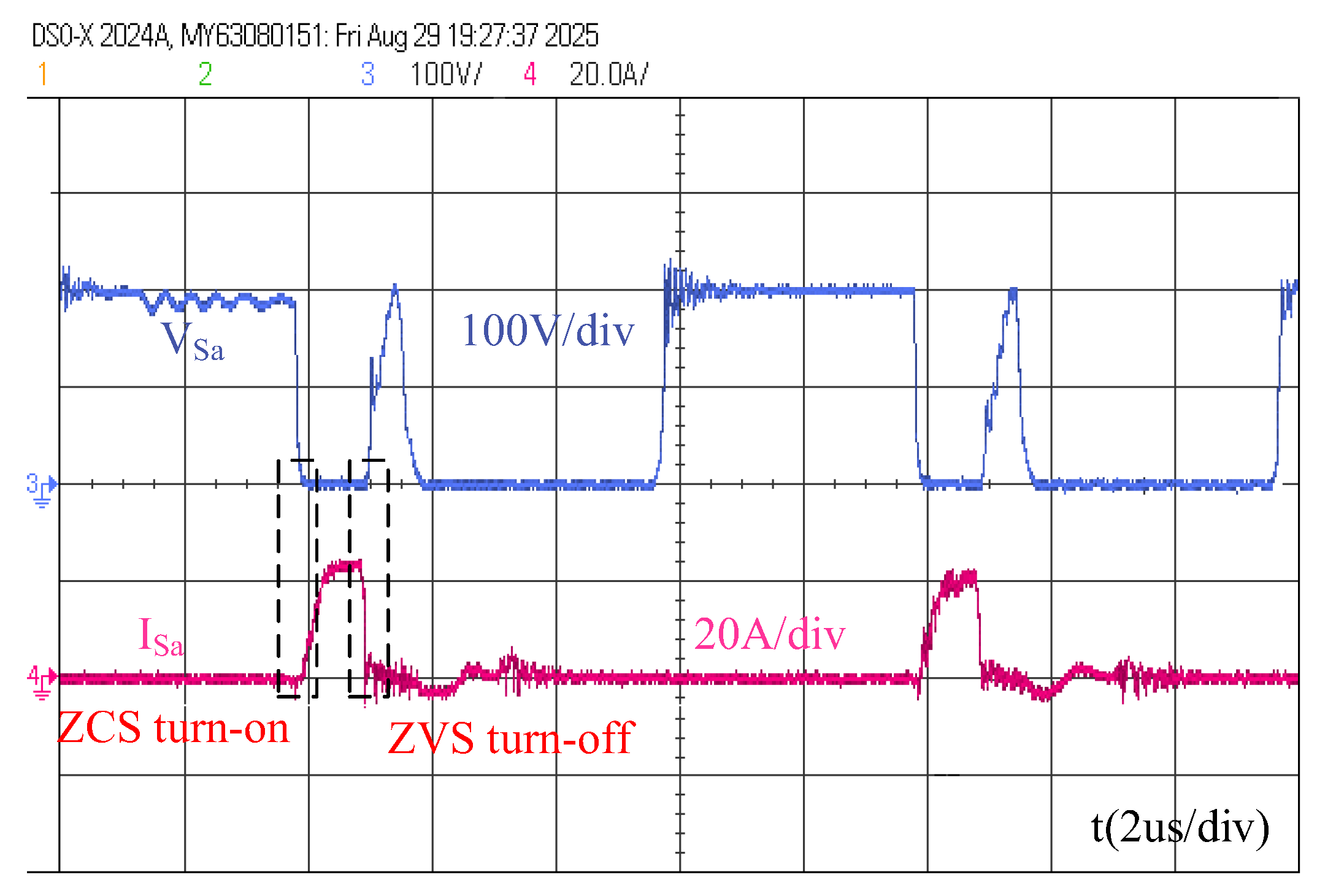
Figure 10 illustrates the measured soft-switching behavior of the auxiliary switch Sa. As observed, the drain–source voltage VSa and drain current iSa confirm that the auxiliary switch Sa turns on under ZCS conditions due to the series resonant inductor. Once the device enters the on-state, the current through Sa rises in linear manner, while the drain–source voltage VSa falls to zero whereas iSa stays low, thereby achieving a soft turn-on transition. During turn-off, Sa operates under ZVS conditions because of the parallel resonant capacitor, which allows the voltage across the switch to rise only after the current has decayed to zero. Consequently, both ZCS turn-on and ZVS turn-off are achieved, resulting in very low switching losses in the auxiliary circuit. Moreover, as the auxiliary switch operates for only a brief interval in each cycle, the associated conduction losses in the auxiliary path are substantially reduced. Therefore, the introduction of the auxiliary circuit adds only minimal conduction losses while effectively reducing the overall switching losses of the main switches.
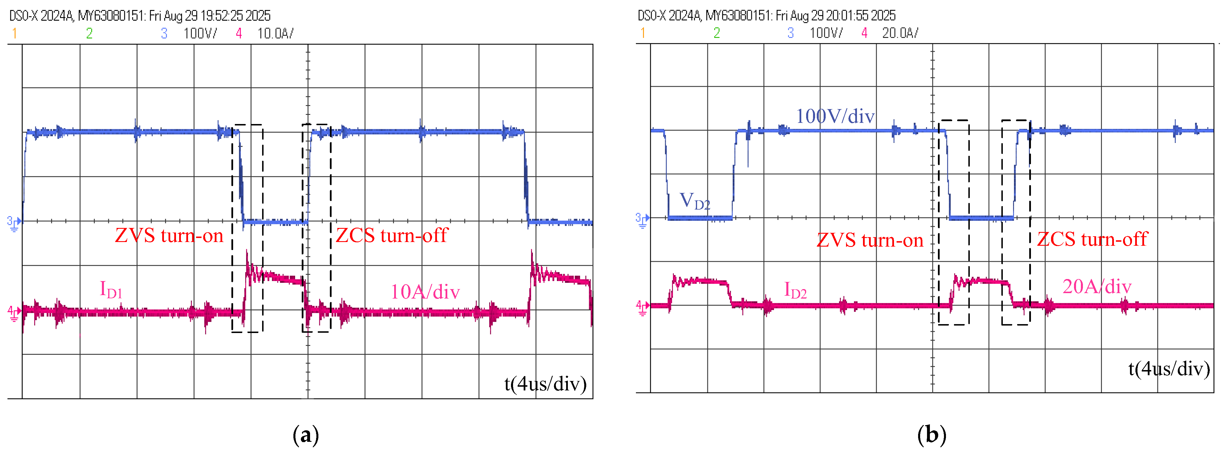
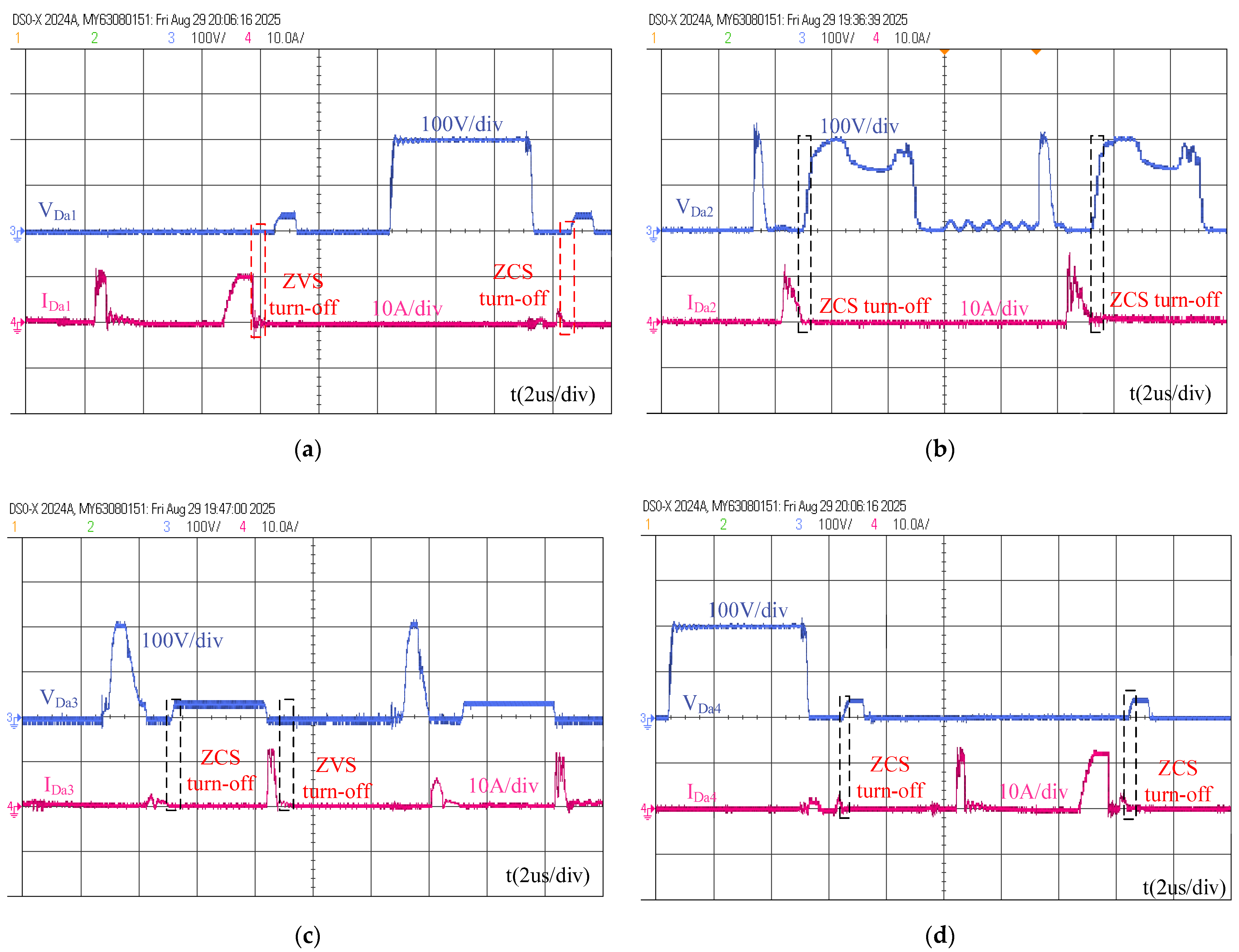
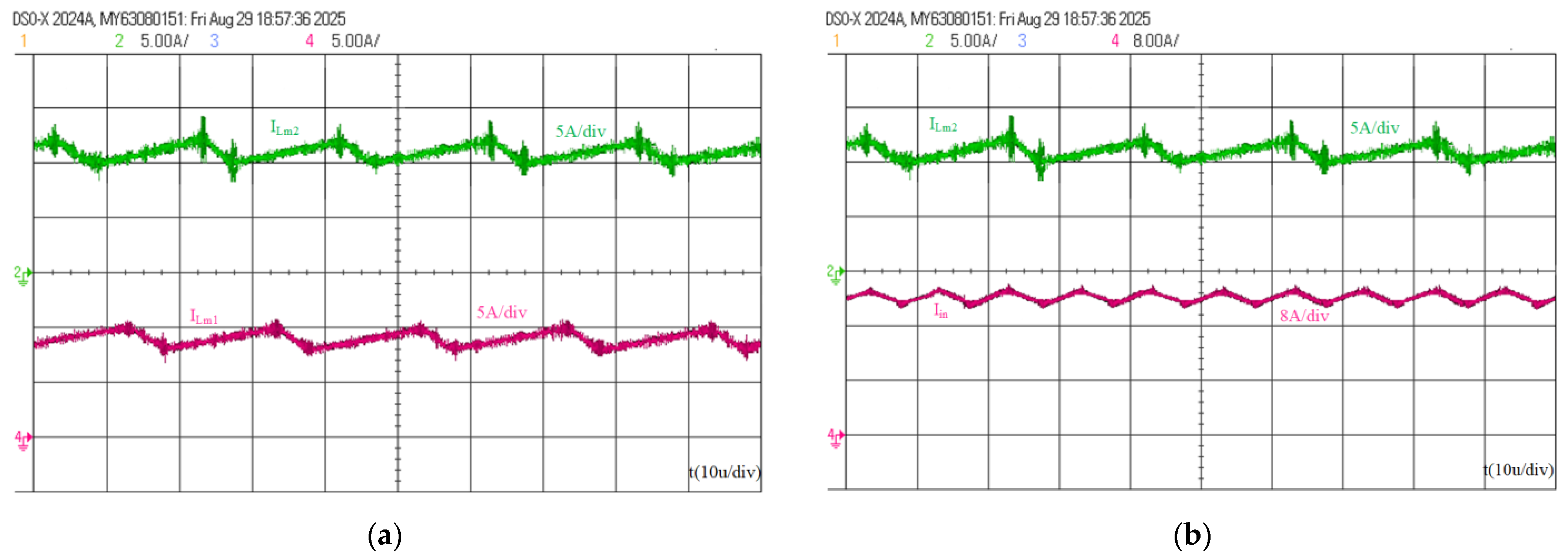
The experimental waveforms of D1 and D2 are illustrated in Figure 11a and Figure 11b, respectively. As demonstrated in Figure 11a,b, the diode D1 and D2 is turned on with ZVS and turned off with ZCS. The reverse-recovery losses of the main diode were eliminated because the main diode turned off with ZCS due to the series inductor. In addition, the voltage stress across D1 and D2 is limited to about 200 V, i.e., nearly half of the output voltage, which shows that the proposed converter effectively reduces the voltage stress on the diodes. Figure 12a–d shows the voltage and current waveforms of the voltage, as well as current waveforms of the auxiliary diodes Da1, Da2, Da3, and Da4. All the diodes turn off under soft-switching conditions, which eliminates reverse-recovery losses. Moreover, the voltage stress across each auxiliary diode is only half of the output voltage. For evaluating the converter’s stability under dynamic conditions, the input voltage was varied between 50 V and 80 V. The respective waveforms for the input voltage, input current, and output voltage are presented in Figure 8b. Despite the changes in input voltage, the output voltage remains stable around the reference value of 400 V. This indicates that the converter can maintain a consistent output voltage across a range of input voltages. Therefore, the converter demonstrates strong dynamic stability. At rated power, the converter’s inductor currents ILm1 and ILm2 and the input current Iin are shown in Figure 13. Figure 13a presents ILm1 and ILm2 for an input of 50 V and an output of 400 V. Both inductor currents exhibit continuous conduction and are 180° out of phase, with nearly identical average values. Figure 13b compares the input current Iin with ILm2; the input current is roughly twice that of iLm2 and exhibits significantly lower ripple than the inductor currents.
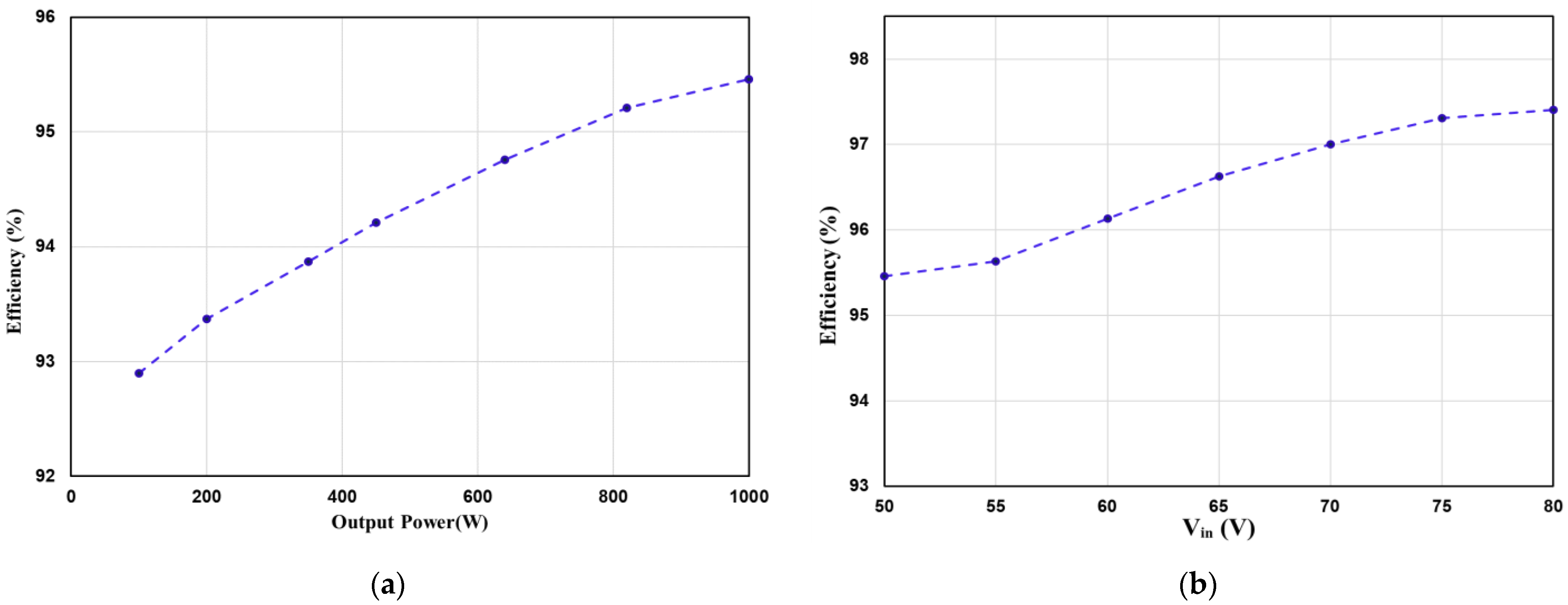
The measured efficiency characteristics are presented in Figure 14. As observed from Figure 14a, the efficiency of the proposed converter varies with the output power level. The proposed converter achieves over 92.5% efficiency across most load conditions. Under light-load operation, the efficiency is approximately 92.9% whereas at rated power, the peak efficiency reaches 95.46%. Figure 14b illustrates how efficiency changes with respect to input voltage for a 1 kW, 400 V output. At Vin = 50 V, the minimum efficiency is 95.46% while the highest efficiency of 97.41% occurs when Vin = 80 V. Moreover, due to the soft-switching operation of the converter, switching losses are inherently minimized. As a result, the overall efficiency improves with increasing input volatge.
A comprehensive loss breakdown analysis was conducted to determine the efficiency of the proposed converter. Given the soft-switching operation of the converter, switching losses are assumed to be negligible. The remaining losses are divided into six parts. The first part is the capacitive turn-on loss of the auxiliary switch, which is calculated as 1/2CSaVSa(t0)fs = 0.55 W, where CSa is the switch parasitic capacitance and VS(t0) is the switch voltage before it is turned on. The second part consists of the switch conduction loss, which is computed as RDS(on)(I2Sm1,rms + I2Sm2,rms + I2Sa,rms) = 6.07 W, with RDS(on) representing the static drain-to-source on-resistance. The third part corresponds to the conduction loss in the diodes, calculated as VF (ID1,avg + ⋯ + IDa4,avg) = 21.76 W, where VF is the instantaneous forward voltage. The fourth part includes the conduction loss of the input inductors and auxiliary inductor, calculated as rLm(I2Lm1,rms + I2Lm2,rms) + rLaI2La,rms = 4.07 W, where rLm and rLa are the resistances of Lm and La, respectively. The fifth part is the ESR loss in the capacitors, calculated as (I2C1,rms + I2C2,rms + I2C3,rms)rc = 10.56 W, where rc is the series resistance. The sixth part is the inductor core loss, calculated as Pcore = PvVe = 2.52 W, where Pv is the core loss density and Ve is the effective core volume. Additionally, approximately 2 W is attributed to miscellaneous losses in the prototype, including PCB trace conduction losses, parasitic resistances, gate drive consumption, and minor switching-related losses not explicitly modeled.


5. Conclusions

In this study, a novel soft-switched interleaved DC-DC boost converter with a common ground is proposed, specifically designed for high-voltage and high-power applications operating in CCM. Compared to traditional non-isolated topologies, the proposed converter provides simultaneous benefits of small input-current ripple, high step-up ratio, and reliable soft-switching operation during turn-on and turn-off events, all within a structurally simple auxiliary circuit. Furthermore, the voltage stress across each switching device and capacitor is limited to half of the total output voltage. An auxiliary circuit is introduced, which, despite minor conduction losses, significantly reduces the switching losses in the main power devices, resulting in high overall efficiency. Experimental results validate the proposed design and confirm its effectiveness. Hence, the proposed converter presents itself as an effective power interface solution between a fuel cell source and a high-voltage DC bus, making it well-suited for use in fuel cell-based power conditioning systems. Despite these advantages, the proposed converter is a non-isolated topology, which may limit its use in applications where galvanic isolation is required for safety. Future work will focus on extending the proposed interleaved high-gain topology to include isolation while retaining the single auxiliary ZVT/ZCS circuit, high voltage gain, low input-current ripple, and soft-switching operation. In addition, the converter will be further evaluated at higher power levels and a wider input voltage range to demonstrate scalability and practical applicability in EV fuel cell systems.

Author Contributions

A.A.S.: Wrote the original draft, analysis, simulation, and experiment design. J.C.: Reviewed the manuscript, supervision, and provided resources, methodology. Y.H.: Reviewed the manuscript, supervision, and contributed to the methodology. A.A.: Provided resources and contributed to the conceptual framework. I.H.: Data analysis and formulation. A.B.: Assisted with conducting experiments. All authors have read and agreed to the published version of the manuscript.

Funding

This research was funded by Andres Annuk, the Energy Efficiency and Renewable Energy Research Infrastructure project of the Estonian Research Council under Grant TARISTU24-TK12.

Data Availability Statement

No datasets were generated or analyzed during the current study. Data is provided within the manuscript.

Conflicts of Interest

The authors declare no competing interests.

References

  1. Li, L.; Coskun, S.; Zhang, F.; Langari, R.; Xi, J. Energy management of hybrid electric vehicle using vehicle lateral dynamic in velocity prediction. IEEE Trans. Veh. Technol. 2019, 68, 3279–3293. [Google Scholar] [CrossRef] [Scilit]
  2. Du, G.; Cao, W.; Hu, S.; Lin, Z.; Yuan, T. Design and assessment of an electric vehicle powertrain model based on real-world driving and charging cycles. IEEE Trans. Veh. Technol. 2019, 68, 1178–1187. [Google Scholar] [CrossRef] [Scilit]
  3. Santi, E.; Franzoni, D.; Monti, A.; Patterson, D.; Ponci, F.; Barry, N. A fuel cell based domestic uninterruptible power supply. In Proceedings of the APEC. Seventeenth Annual IEEE Applied Power Electronics Conference and Exposition (Cat. No. 02CH37335); IEEE: Piscataway, NJ, USA, 2002; pp. 605–613. [Google Scholar]
  4. Hussain, I.; He, Y.; Khan, M.M.; Khan, A.U.; Samejo, A.A.; Annuk, A. Optimal design and sensitivity analysis of a dual active bridge converter for electrolyzer-based hydrogen production. J. Power Sources 2026, 676, 239923. [Google Scholar] [CrossRef] [Scilit]
  5. Wu, X.; Yang, M.; Zhou, M.; Zhang, Y.; Fu, J. A novel high-gain DC–DC converter applied in fuel cell vehicles. IEEE Trans. Veh. Technol. 2020, 69, 12763–12774. [Google Scholar] [CrossRef] [Scilit]
  6. Sha, D.; Xu, Y.; Zhang, J.; Yan, Y. Current-fed hybrid dual active bridge DC–DC converter for a fuel cell power conditioning system with reduced input current ripple. IEEE Trans. Ind. Electron. 2017, 64, 6628–6638. [Google Scholar] [CrossRef] [Scilit]
  7. Elsayad, N.; Moradisizkoohi, H.; Mohammed, O.A. A single-switch transformerless DC–DC converter with universal input voltage for fuel cell vehicles: Analysis and design. IEEE Trans. Veh. Technol. 2019, 68, 4537–4549. [Google Scholar] [CrossRef] [Scilit]
  8. Zuo, D.B.; Cobaleda, X.; Shen, W.; Martinez, W. High Step-up Ratio Interleaved Boost L-LLC Resonant Converter with PWM and PFM Control for Wide Input and Output Voltage Range. In Proceedings of the 2024 IEEE Applied Power Electronics Conference and Exposition (APEC), Long Beach, CA, USA, 2024; IEEE: Piscataway, NJ, USA, 2014; pp. 1396–1402. [Google Scholar]
  9. Zuo, X.; Shen, B.; Du, D.B.; Cobaleda, H.; Wouters, W.; Martinez, W. Fixed-frequency Dual PWM Interleaved Boost LLC Resonant Converter for a Wide Input Voltage for Photovoltaic Applications. In Proceedings of the 2024 IEEE 10th International Power Electronics and Motion Control Conference (IPEMC2024-ECCE Asia), Chengdu, China, 17–20 May 2024; IEEE: Piscataway, NJ, USA, 2024; pp. 4172–4177. [Google Scholar]
  10. Han, J.; Kim, J.; Lee, B.; Lai, J.; Moon, G. High-efficiency asymmetrical half-bridge converter with a new coupled inductor rectifier (CIR). IEEE Trans. Power Electron. 2019, 34, 11541–11552. [Google Scholar] [CrossRef]
  11. Wang, Z.; Wang, P.; Bi, H.; Qiu, M. A bidirectional DC/DC converter with wide-voltage gain range and low-voltage stress for hybrid-energy storage systems in electric vehicles. J. Power Electron. 2020, 20, 76–86. [Google Scholar] [CrossRef] [Scilit]
  12. Forouzesh, M.; Siwakoti, P.Y.; Gorji, A.S.; Blaabjerg, F.; Lehman, B. Step-up DC–DC converters: A comprehensive review of voltage boosting techniques, topologies, and applications. IEEE Trans. Power Electron. 2017, 32, 9143–9178. [Google Scholar] [CrossRef] [Scilit]
  13. Lakshmi, M.; Hemamalini, S. Nonisolated high gain DC-DC converter for DC microgrids. IEEE Trans. Power Electron. 2018, 65, 1205–1212. [Google Scholar] [CrossRef] [Scilit]
  14. Zhang, Y.; Liu, Q.; Li, J.; Sumner, M. A common ground switched quasi-z-source bidirectional DC-DC converter with wide-voltage-gain range for EVs with hybrid energy sources. IEEE Trans. Ind. Electron. 2018, 65, 5188–5200. [Google Scholar] [CrossRef] [Scilit]
  15. Bi, H.; Wang, P.; Che, Y. A capacitor clamped H-type boost DC-DC converter with wide voltage-gain range for fuel cell vehicles. IEEE Trans. Veh. Technol. 2019, 68, 276–290. [Google Scholar] [CrossRef] [Scilit]
  16. Chen, S.; Zhou, L.; Luo, Q.; Gao, W.; Wei, Y.; Sun, P.; Du, X. Research on topology of the high step-up boost converter with coupled inductor. IEEE Trans. Power Electron. 2019, 34, 10733–10745. [Google Scholar] [CrossRef] [Scilit]
  17. Wu, H.; Sun, K.; Chen, L.; Zhu, L.; Xing, Y. High step-up/step-down soft-switching bidirectional DC-DC converter with coupled-inductor and voltage matching control for energy storage systems. IEEE Trans. Ind. Electron. 2016, 63, 2892–2903. [Google Scholar] [CrossRef] [Scilit]
  18. Wang, Y.; Qiu, Y.; Bian, Q.; Guan, Y.; Xu, D. A single switch quadratic boost high step-up DC-DC converter. IEEE Trans. Ind. Electron. 2019, 66, 4387–4397. [Google Scholar] [CrossRef] [Scilit]
  19. Zhang, F.; Xie, Y.; Hu, Y.; Chen, G.; Wang, X. A hybrid boost-flyback/flyback microinverter for photovoltaic applications. IEEE Trans. Ind. Electron. 2020, 67, 308–318. [Google Scholar] [CrossRef] [Scilit]
  20. Liu, H.; Li, F. Novel high step-up DC-DC converter with an active coupled-inductor network for a sustainable energy system. IEEE Trans. Power Electron. 2015, 30, 6476–6482. [Google Scholar] [CrossRef] [Scilit]
  21. Hu, X.; Li, L.; Li, Y.; Wu, G. Input-parallel output-series DC-DC converter for non-isolated high step-up applications. Electron. Lett. 2016, 52, 1715–1717. [Google Scholar] [CrossRef] [Scilit]
  22. Bi, H.; Jia, C. Common grounded wide voltage-gain range DC-DC converter for fuel cell vehicles. IET Power Electron. 2019, 12, 1195–1204. [Google Scholar] [CrossRef] [Scilit]
  23. Dang, Z.; Abu Qahouq, J.A. Permanent-magnet coupled power inductor for multiphase DC-DC power converters. IEEE Trans. Ind. Electron. 2017, 64, 1971–1981. [Google Scholar] [CrossRef] [Scilit]
  24. Lee, P.-W.; Lee, Y.-S.; Cheng, D.K.W.; Liu, X.-C. Steady-state analysis of an interleaved boost converter with coupled inductors. IEEE Trans. Ind. Electron. 2000, 47, 787–795. [Google Scholar] [CrossRef] [Scilit]
  25. Chen, Y.; Li, Z.; Liang, R. A novel soft-switching interleaved coupled inductor boost converter with only single auxiliary circuit. IEEE Trans. Power Electron. 2018, 33, 2267–2281. [Google Scholar] [CrossRef] [Scilit]
  26. Tran, H.N.; Jeong, H.; Kim, S.; Le, T.T.; Choi, S. Interleaved ZVT Boost Converter for 800V Fuel Cell Electric Vehicles. In Proceedings of the 2019 IEEE Vehicle Power and Propulsion Conference (VPPC), Hanoi, Vietnam, 14–17 October 2019; pp. 1–5. [Google Scholar]
  27. Akhlaghi, B.; Farzanehfard, H. Family of ZVT interleaved converters with low number of components. IEEE Trans. Ind. Electron. 2018, 65, 8565–8573. [Google Scholar] [CrossRef]
  28. Prudente, M.; Pfitscher, L.; Emmendoerfer, G.; Romaneli, E.F.; Gules, R. Voltage multiplier cells applied to non-isolated converters. IEEE Trans. Power Electron. 2008, 23, 871–887. [Google Scholar] [CrossRef] [Scilit]
  29. Wang, P.; Zhou, L.; Zhang, Y.; Li, J.; Sumner, M. Input-parallel output-series DC–DC boost converter with a wide input voltage range for fuel cell vehicles. IEEE Trans. Veh. Technol. 2017, 66, 7771–7781. [Google Scholar] [CrossRef] [Scilit]
  30. Martinez, W.; Cortes, C.; Yamamoto, M.; Imaoka, J. Effect of inductor parasitic resistances on the voltage gain of high step-up DC–DC converters for electric vehicle applications. IET Power Electron. 2018, 11, 1628–1639. [Google Scholar] [CrossRef] [Scilit]
  31. Tseng, K.; Huang, C.; Cheng, C. A single-switch converter with high step-up gain and low diode voltage stress suitable for green power source conversion. IEEE Trans. Emerg. Sel. Top. Power Electron. 2016, 4, 363–372. [Google Scholar] [CrossRef] [Scilit]
  32. Baddipadiga, B.P.; Ferdowsi, M. A high-voltage-gain DC–DC converter based on modified Dickson charge pump voltage multiplier. IEEE Trans. Power Electron. 2017, 32, 7707–7715. [Google Scholar] [CrossRef] [Scilit]
  33. Tarzamni, H.; Babaei, E.; Zarrin Gharehkoushan, A.; Sabahi, M. Interleaved full ZVZCS DC–DC boost converter: Analysis, design, reliability evaluations and experimental results. IET Power Electron. 2017, 10, 835–845. [Google Scholar] [CrossRef] [Scilit]
  34. Forouzesh, M.; Shen, Y.; Yari, K.; Siwakoti, Y.P.; Blaabjerg, F. High efficiency high step-up DC–DC converter with dual coupled inductors for grid-connected photovoltaic systems. IEEE Trans. Power Electron. 2018, 33, 5967–5982. [Google Scholar] [CrossRef] [Scilit]
  35. Moradisizkoohi, H.; Elsayad, N.; Mohammed, O.A. An integrated interleaved ultrahigh step-up DC–DC converter using dual cross-coupled inductors with built-in input current balancing for electric vehicles. IEEE J. Emerg. Sel. Top. Power Electron. 2020, 8, 644–657. [Google Scholar] [CrossRef] [Scilit]
  36. Akhlaghi, B.; Molavi, N.; Fekri, M.; Farzanehfard, H. High step-up interleaved ZVT converter with low voltage stress and automatic current sharing. IEEE Trans. Ind. Electron. 2018, 65, 291–299. [Google Scholar] [CrossRef] [Scilit]
  37. Li, B.; Wang, P.; Wang, Z.; Ma, X.; Bi, H. A new coupled-inductor-based high-gain interleaved DC–DC converter with sustained soft switching. IEEE Trans. Veh. Technol. 2021, 70, 6527–6541. [Google Scholar] [CrossRef] [Scilit]
Figure 1. The standard configuration of a fuel cell vehicle.
Machines 14 00485 g001
Figure 2. Proposed Converter: (a) the layout of the converter; (b) operational flowchart.
Machines 14 00485 g002
Figure 3. Key waveforms of the proposed converter.
Machines 14 00485 g003
Figure 4. Equivalent circuits of the operating stages. (a) Stage 1 [Before instant t1], (b) Stage 2 [t1–t2], (c) Stage 3 [t2–t3], (d) Stage 4 [t3–t4], (e) Stage 5 [t4–t5], (f) Stage 6 [t5–t6], (g) Stage 7 [t6–t7], (h) Stage 8 [t7–t8], (i) Stage 9 [t8–t9], (j) Stage 10 [t9–t10].
Machines 14 00485 g004
Figure 5. Proposed converter with parasitic elements.
Machines 14 00485 g005
Figure 6. Key inductor waveforms.
Machines 14 00485 g006
Figure 7. Images of the developed hardware and the laboratory setup: (a) developed hardware, (b) experimental setup.
Machines 14 00485 g007
Figure 8. Performance of the proposed converter: (a) Gate drive signals of the three switches together with the output voltage waveform. (b) Transient response corresponding to an input voltage change between 50 V and 80 V.
Machines 14 00485 g008
Figure 9. Experimental soft-switching performance of (a) Sm1; (b) Sm2.
Machines 14 00485 g009
Figure 10. Experimental soft-switching performance of the auxiliary switch.
Machines 14 00485 g010
Figure 11. Experimental soft-switching performance of (a) D1; (b) D2.
Machines 14 00485 g011
Figure 12. Experimental soft-switching performance of (a) Da1, (b) Da2, (c) Da3, (d) Da4.
Machines 14 00485 g012
Figure 13. Inductor and input currents: (a) inductor currents ILm1 and ILm2; (b) inductor current ILm2 and input current Iin.
Machines 14 00485 g013
Figure 14. Performance efficiency: (a) efficiency versus output power, and (b) efficiency versus input voltage.
Machines 14 00485 g014
Table 1. Comparison of converter topologies.
ConvertersVoltage GainVoltage Stress Across the SwitchesVoltage Stress Across the DiodesSoft-SwitchingNo. of Components (S/D/C/Core)Input-Current RippleCommon Ground
[28] 2 1 D 1 2 V o 1 2 V o Hard Switching2/4/3/2HighYes
[29] 2 1 D 1 2 V o 1 2 V o Hard Switching2/3/3/2SmallNo
[30] D < 0.5 : 1 1 k D D > 0.5 : 1 + N 1 D V o 1 2 V o Hard Switching2/4/1/1SmallYes
[31] n ( 2 + D ) + 3 1 D V o n ( 2 + D ) + 3 n + 1 n ( 2 + D ) + 3 V o Hard Switching1/5/5/1LargeYes
[32] 4 1 D 3 8 V o 1 2 V o Hard Switching2/4/5/2SmallNo
[33] 1 1 D V o V o ZVZCS4/4/3/4SmallYes
[34] 2 n + 1 1 D V o 2 n + 1 ( 2 n + 1 ) V o 2 ( n + 1 ) ZVS4/2/3/2SmallYes
[35] 2 2 n + 1 1 D V o 2 2 n + 1 1 2 V o ZVS4/4/5/1SmallNo
[36] 2 n + 2 1 D V o 2 n + 2 n + 1 n + 2 V o ZVS/ZCS3/6/4/2SmallNo
[37] 1 Q + 0.5 D 1 2 V o 1 2 V o ZVS/ZCS3/3/3/1Very SmallYes
Proposed Converter 2 1 D 1 2 V o 1 2 V o ZVS/ZCS3/3/4/3Very SmallYes
Table 2. Experimental parameters of the converter.
SpecificationSymbolValue
Input VoltageVin50 V
Output VoltageVo400 V
Output PowerPo1 kW
Switching Frequencyfs50 kHz
Main Boost Inductor Lm1, Lm2330 μH
Output Capacitor C1, C2, C3270 μF
Resonant InductorLa10 μH
Resonant CapacitorCa3.3 nF
Main SwitchesSm1, Sm2IRF300P226
Auxiliary SwitchSaIRF300P226
Main DiodesD1, D2, D3VS-60APH03-N3
Auxiliary DiodesDa1, Da2, Da3, Da4VS-60APH03-N3
Disclaimer/Publisher’s Note: The statements, opinions and data contained in all publications are solely those of the individual author(s) and contributor(s) and not of MDPI and/or the editor(s). MDPI and/or the editor(s) disclaim responsibility for any injury to people or property resulting from any ideas, methods, instructions or products referred to in the content.