
Article

Research on Thermal Analysis and Enhanced Heat Dissipation Technology of Fully Enclosed Reinforced Computer

State Key Laboratory of Electromechanical Integrated Manufacturing of High-performance Electronic Equipment, School of Mechatronic Engineering, Xidian University, Xi’an 710071, China
*
Author to whom correspondence should be addressed.
Machines 2025, 13(11), 1067; https://doi.org/10.3390/machines13111067
Submission received: 27 September 2025 / Revised: 9 November 2025 / Accepted: 18 November 2025 / Published: 19 November 2025
(This article belongs to the Section Machine Design and Theory)

Abstract

Fully enclosed reinforced computers typically need to adapt to harsh environments such as high temperature, humidity, and strong vibration. However, their physical hermeticity leads to a single heat dissipation method, and local overheating caused by high heat flux density components seriously threatens equipment reliability. To address this issue, this study first analyzed its structural characteristics and established a cross-scale simulation model of the chassis and board. Second, aiming at internal heat accumulation and local overheating at high temperatures, the problem was solved by optimizing the layout of components on the motherboard. For thermo-mechanical collaborative optimization of these components, a Pareto-max-min ant algorithm was designed, adopting dynamic state transition, hybrid local search, pheromone update, and Pareto solution set update strategies to obtain the Pareto frontier. The optimal solution was selected via the LINMAP decision method and simulated, and the optimal layout of the fan module was determined. Finally, a prototype was manufactured, and temperature field tests were conducted. Results show that at 25 °C~55 °C, all chips’ temperatures are below the allowable limit, with errors within 10% vs. simulation data, verifying the thermal simulation and design.

1. Introduction

With the intelligent development of modern military equipment, the refinement of industrial control systems, and the increasing complexity of deep-space exploration missions, the operating environments of electronic devices have expanded from traditional laboratory settings to extreme conditions such as high temperature, high humidity, strong vibration, heavy dust, and vacuum radiation. Taking military scenarios as an example, computers integrated into equipment like armored vehicles, shipborne command systems, and airborne radars must operate stably within a temperature range of −40 °C to 55 °C (GJB 322A-1998) [1]. They must also withstand impact vibrations of over 10 g and meet the IP68 standard for water and dust resistance.
If such devices adopt an open-type heat dissipation design, the intrusion of external contaminants will cause circuit corrosion, while vibrations may lead to failures of moving components such as fans. Therefore, fully enclosed ruggedized computers, leveraging their physical isolation properties, have become a viable carrier for electronic systems in extreme environments and are widely used across various industries.
The hermetic design improves reliability while completely blocking the implementation of active cooling methods such as air cooling and liquid cooling, making the computer heat dissipation problem a core bottleneck restricting its performance [2,3]. Moreover, the exponential growth in power density of electronic devices has intensified the heat dissipation challenge. The power consumption of core chips such as high-performance computing units like CPU, FPGA, and GPU continues to rise, with heat flux exceeding 100 W/cm2. Additionally, the continuous development of computer modules towards miniaturization and integration has led to multiple PCB system boards being packaged in a high-density stacked manner within narrow chassis [4], further compressing the heat dissipation space [5,6,7]. Studies have shown that the reliability of power devices is closely related to their temperature. The U.S. Air Force Overall Program Analysis Report points out that more than half of the failures in electronic devices are caused by high temperatures. Furthermore, non-uniform thermal stress caused by local hotspots can lead to structural failures such as solder ball cracking and substrate warping, and may even cause the computer to restart or shut down due to thermal runaway, resulting in serious consequences [8,9,10]. Therefore, to ensure the reliable operation of fully hermetic ruggedized computers, thermal simulation and thermal optimization design for them are particularly important.
Currently, for addressing the heat dissipation issues of electronic devices, traditional methods mainly include the design and optimization of physical devices such as heat pipes, vapor chambers, heat sink structures, and fans. Simulation tools are used to model and analyze the hermetic chassis, and verification is conducted through experimental data to improve heat conduction efficiency [11,12,13]. However, most structural optimization work aims to reduce the maximum temperature of a single chip or component, without fully considering the mutual influence between heat sources [14,15,16]. In the thermal optimization design of the fully hermetic ruggedized computer in this paper, the thermal coupling effect between various chips is considered, thermal design is carried out through thermal optimization layout, and thermal simulation analysis and experiments are conducted for verification.
In the current layout optimization of PCB-mounted components, attention is mostly limited to thermal performance alone, and the coupling effects between thermal and mechanical multi-physics fields are rarely taken into account [17]. Through optimization, local hotspots of components and the heat flux coupling effect between components can be reduced [18,19]. The second part is the layout optimization for all internal modules of electronic devices to improve the air flow distribution inside the chassis [20,21]. Optimization enables the device to develop towards miniaturization and centralization while meeting the heat dissipation performance of components. At present, the layout optimization of components on PCB boards only focuses on single thermal performance [22], without considering the coupling effect between thermal-mechanical-electrical multi-physics fields [23,24,25]; for the systematic research on the overall layout of fully hermetic structures (such as fans, control modules, etc.), more attention is paid to open or semi-closed chassis systems and external cooling methods (such as air cooling/liquid cooling) [26], ignoring the problem of internal air flow organization and layout optimization in hermetic structures [27,28,29]. To solve the above problems, this paper not only optimizes the temperature field distribution through thermal-mechanical coupling optimization but also considers the mechanical stress and deformation of the PCB. It proposes an improved Pareto max-min ant colony algorithm combined with LINMAP for multi-objective optimal solution selection to scientifically select the optimal layout solution, thereby improving the heat dissipation performance of the entire machine’s cooling system.
The remainder of this paper is organized as follows: Section 2 presents the structural configuration of each module in the ruggedized computer, the thermal-mechanical coupling method, the set up of boundary conditions, and the thermal simulation of the initial model. Section 3 describes the thermal optimization design method for the ruggedized computer and the corresponding optimization results, which are compared with the simulation results of the initial model. Section 4 conducts thermal tests on the engineering prototype fabricated based on the thermally optimized design, and compares and analyzes the test results with the thermal optimization simulation results to verify the heat dissipation performance of the fully enclosed ruggedized computer. Section 5 draws the conclusions.

2. Model

In fully enclosed reinforced computers, the heat flux coupling effect between compactly arranged components becomes significant when the ambient temperature reaches 55 °C. To address this issue, thermal optimization design was conducted at both the board and system levels. For the thermal design optimization of component layout on the PCB, a Pareto-max-min ant algorithm was employed, integrating dynamic state transition strategy, hybrid local search strategy, multi-objective pheromone update strategy, and Pareto solution set update strategy. After selecting the optimal layout via the LINMAP decision method, a new model was established for thermal simulation, with results compared and analyzed against those before optimization. Additionally, the orthogonal test method was used to optimize the layout of functional modules inside the chassis. A new model was also built for thermal simulation of the optimal layout, followed by comparison and analysis with pre-optimization results.

2.1. The Basic Analysis of Fully Enclosed Ruggedized Computers

2.1.1. Structural Characteristics of Fully Enclosed Ruggedized Computers

Fully enclosed ruggedized computers typically operate in harsh environments (such as high temperature, high humidity, mold, salt spray, and electromagnetic interference). To meet their operational requirements while ensuring high reliability, a fully enclosed system design is adopted. Specifically, electronic components, circuit boards, power modules, and other components are all housed within a sealed chassis, with only a PCIe interface for external connection, forming a complete enclosed system. This design ensures its performance in terms of waterproof, dustproof, anti-corrosion (three-proof) capabilities and electromagnetic shielding.
The overall and internal structure diagrams of the engineering prototype for the fully enclosed ruggedized computer are shown in Figure 1. The internal structure of the fully enclosed ruggedized computer mainly consists of three parts: the motherboard module, the heat pipe module, and the control module. Key power components are concentrated on the motherboard module, specifically including Chip 3A6000, Chip 7A2000, Chip X100, DDR4 memory, Chip 1860, Chip 2329, and Chip a200. The motherboard is connected to the chassis via bolts in an inverted state, allowing the main heat-generating components to contact the heat pipe module through heat-conducting blocks, with the heat pipe module fixedly attached to the inner shell of the chassis. Externally, it mainly comprises a chassis outer shell and two turbo fans embedded in the chassis shell.

2.1.2. Thermal-Mechanical Coupling Equations for the Fully Enclosed Ruggedized Computer

The thermal-mechanical coupling of fully enclosed ruggedized computers is the core contradiction. The thermal field generates thermal stress through temperature gradients, while the mechanical field alters heat conduction paths (such as contact thermal resistance) through deformation. Their mutual interaction directly affects the reliability of the equipment.
  • Governing Equations of the Thermal Field
The thermal field equations cover “heat conduction in the solid domain” and “convective heat transfer of air inside the chassis”. As one of the heat transfer paths, air convection, although not directly involved in the mechanical field coupling, affects heat distribution and thereby changes thermal stress, so it needs to be included in the model. Meanwhile, emphasis is placed on the excitation effect of temperature distribution in the solid domain on the mechanical field.
First, based on the law of energy conservation, the thermal field of the fully enclosed ruggedized computer follows Fourier’s law of heat conduction and the convective heat transfer equation. Considering the steady-state heat transfer scenario, the heat conduction equation for the solid domain is as follows:
k s T + q v = 0
Herein, k s represents the thermal conductivity of the solid material, T denotes the temperature (in Kelvin, K), and q v stands for the volumetric heat source intensity.
The convective heat transfer equation for the fluid domain (air inside the chassis) is as follows:
ρ f C p u T = k f T + q c o n v
Herein, ρ f denotes the air density, C p represents the air’s specific heat capacity at constant pressure, u stands for the air velocity vector, k f is the air thermal conductivity, and q c o n v refers to the convective heat transfer source term between the fluid and the solid wall.
2.
Governing Equations of the Mechanical Field
Based on the law of conservation of momentum, the mechanical field focuses on the vibration and shock responses of the PCB and components, which are described using elastic mechanics equations. The vibration response equation is as follows:
M d ¨ + C d ˙ + K d = F t
Herein, M is the mass matrix, C denotes the damping matrix, K represents the stiffness matrix, d stands for the displacement vector (in m), and F t refers to the time-dependent external force vector (such as vibration excitation and impact load).
The stress–strain relationship is as follows:
σ = E ε
Herein, σ is the stress, E denotes the elastic modulus of the material, and E represents the strain. The strain ε and displacement d satisfy the geometric equation:
ε = 1 2 d + d T
3.
Direct Thermal-mechanical Field Coupling Relationship
The thermal field influences the mechanical field through the “temperature-material property” correlation, with the core coupling term being thermal strain:
ε t h = α Δ T
Herein, α is the thermal expansion coefficient of the material, and Δ T is the temperature change. Thermal strain is superimposed on mechanical strain, leading to a redistribution of structural stress, i.e., thermal stress σ t h = E α Δ T , which ultimately affects the deformation and vibration response of the PCB.

2.1.3. Hierarchical Multi-Scale Classification and Boundary Condition Configuration for Fully Enclosed Ruggedized Computer

In the cross-scale equivalent modeling of fully enclosed ruggedized computers, the scaling rules for geometric features represent a core technical approach to balancing model accuracy and computational efficiency. Specifically, three scales are defined: macroscale, mesoscale, and microscale.
  • Macroscale (1 cm–50 cm)
The macroscale primarily involves modeling the chassis enclosure and internal modules. The enclosure of fully enclosed ruggedized computers is typically fabricated via integral casting of high-strength aluminum alloy, with its external fins retained in the model. Key heat-generating components within the chassis—including Chip 3A6000, Chip 7A2000, Chip X100, and DDR4 memory—are equivalently modeled using shell elements.
Flow boundary conditions: First, for the inlet of the internal air domain is defined as a “pressure inlet” with a pressure equal to atmospheric pressure and a temperature set to the ambient temperature. Next is the fan outlet. Fan performance affects the air flow velocity inside the chassis, and the velocity directly determines the convective heat transfer coefficient. Therefore, in the simulation, the fan outlet velocity is correlated with the air volume and defined as a “velocity outlet”. For simplification of the simulation, the flow velocity is set to 10 m/s. Additionally, a “fan boundary” is added with a pressure rise of Δ P = 150 Pa which is also set as a fixed value. Finally, solid walls (including the inner chassis surfaces and module housings) are assigned “no-slip boundaries” (i.e., u = 0 ). The convective heat transfer coefficient h is calculated via empirical correlations, with a base range of 10~20 W / m 2 K , adjusted according to air flow velocity.
2.
Mesoscale (1 mm–10 mm)
The mesoscale focuses on modeling components with significant local effects, specifically heat pipes, fins, and thermal conduction blocks, as these directly influence heat transfer efficiency. Mesh resolution at this scale must satisfy a wall thickness constraint of ≤2 mm, with boundary layer meshes consisting of at least 5 layers and a growth rate ≤ 1.2.
Flow boundary conditions: First, the inner wall of the heat pipe is defined as a “heat flux boundary” where the heat flux equals the heat transferred from the chip to the heat pipe. Second, the fin surface is designated as a “convective heat transfer boundary”. Considering the influence of fin spacing on flow velocity, the convective heat transfer coefficient is corrected as h f i n = 1.2 h.
3.
Microscale (1 μm–1 mm)
Microscale modeling primarily includes layered chip structures, specifically the substrate layer and solder ball layer. Challenges at this scale include geometric complexity, computational resource limitations, multiphysics coupling, material inhomogeneity, and difficulties in experimental validation. To address these, an equivalent modeling method is applied to chip solder balls to ensure simulation feasibility.
Flow boundary conditions: Frist, the contact interface between solder balls and the chip substrate is set as an “isothermal boundary” with a temperature equal to the chip core temperature. The interface between solder balls and the PCB is defined as a “thermal resistance boundary,” where thermal resistance R = δ / k A ( δ = solder ball height, k = thermal conductivity of solder ball material, A = contact area) to simulate contact thermal resistance between solder balls and the PCB.
After configuring flow boundaries (primarily for cross-scale coupling), heat transfer boundary conditions are established to address multiphysics coupling at thermal-mechanical interfaces:
The configuration of flow boundaries primarily targets cross-scale coupling. Once completed, the heat transfer boundary conditions are set, focusing on multiphysics coupling at thermal-mechanical interfaces. First, the bolts connecting the PCB to the chassis are assigned “fixed temperature + displacement constraint”: the temperature is set equal to that of the chassis shell, and the displacement is d = 0 (simulating mechanical constraints from bolt fastening while enabling heat transfer). Second, the interfaces between components and the PCB are defined as “thermal conduction + contact stiffness constraint”: the thermal conductivity is taken as the average of the two materials, and the mechanical contact stiffness is set to K c o n t a c t = 10 6 N/m (simulating mechanical fixation and heat transfer from component mounting).
For the environmental boundary, the outer surface of the chassis shell is defined as a “convection boundary,” with parameter settings including the following components:
(1)
Operating temperature range of the device: 25 °C to 55 °C.
(2)
Thermal conductivity of air: 10 W / m 2 ° C ; thermal conductivity of stagnant air: 5 W / m 2 ° C .
For the material properties, details are presented in Table 1.
Regarding power consumption values, the design power consumption and allowable temperature range of each device are presented in Table 2.
Among them, the length of the heat pipe in contact with Chip 3A6000 is 234 mm, with an evaporator section length of 40 mm and a condenser section length of 30 mm. The heat pipe in contact with Chip 7A2000 has a total length of 232 mm, an evaporator section of 40 mm, and a condenser section of 30 mm. The heat pipe in contact with Chip X100 measures 172 mm in total length, with an evaporator section of 30 mm and a condenser section of 30 mm. The internal heat transfer of the heat pipe involves four stages: “liquid evaporation in the evaporator section → vapor flow → vapor condensation in the condenser section → capillary reflux in the wick”. The total internal thermal resistance R c o n d 0.0019 K/M of the pipe is obtained through simplified calculation using equivalent thermal resistance.

2.2. Thermal Simulation Analysis of Fully Enclosed Ruggedized Computers

2.2.1. Establishment of Geometric Models

This paper takes fully enclosed ruggedized computers as the research object for modeling, and the specific parameters of the equipment and its components are shown in Table 3.
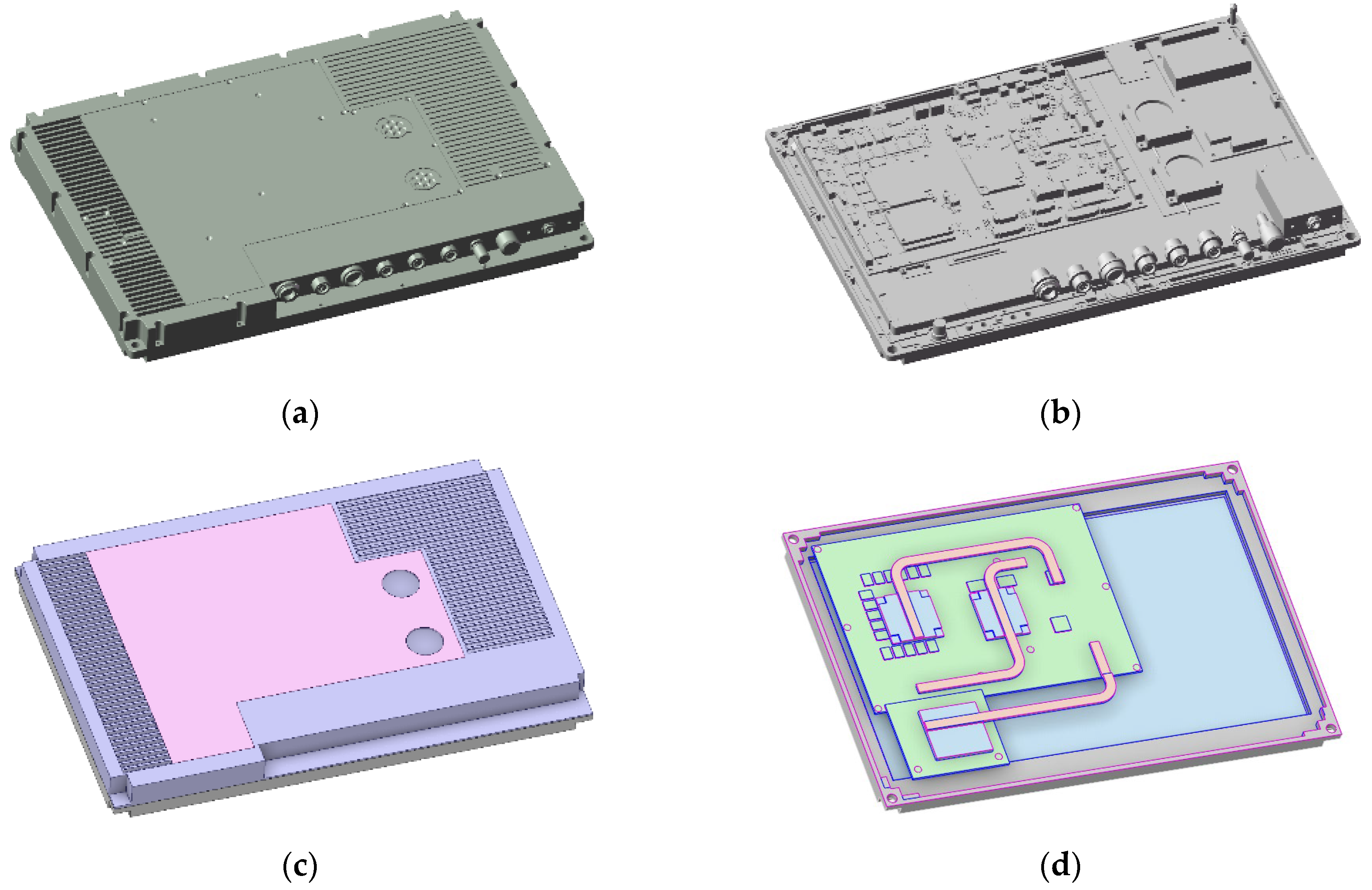
The fully enclosed ruggedized computer was modeled using SolidWorks 2022 SP0.0, as shown in Figure 2a,b. The model was then simplified using SpaceClaim 2022 (Version: 2022.1.0.11304), with key heat-generating components and primary heat dissipation pathways retained (see Figure 2c,d for details). During simplification, features such as small holes (diameter < 5 mm) and chamfers on the chassis were omitted. Additionally, components like capacitors and resistors, which have a negligible impact on the overall thermal-mechanical behavior, were also simplified. This simplification significantly improves computational efficiency and reduces modeling complexity while ensuring simulation accuracy, adhering to the core principle of “focusing on primary factors and neglecting secondary ones” in engineering simulations.
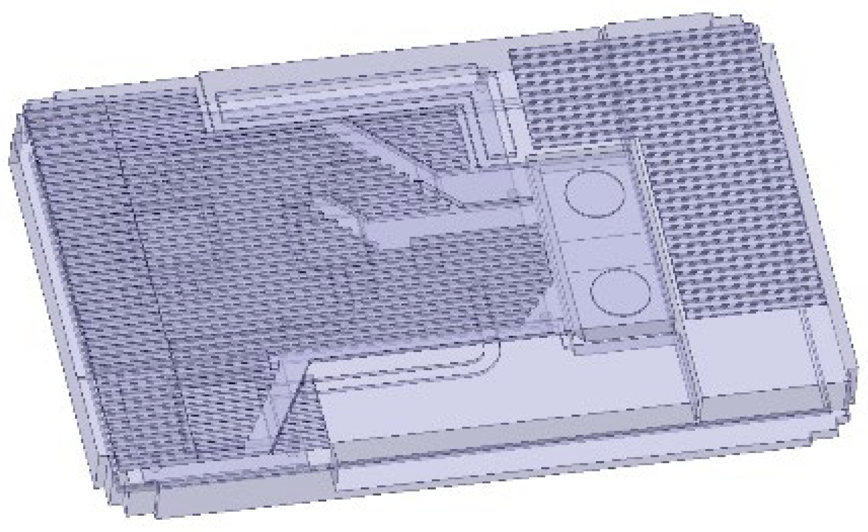
It should be noted that when conducting thermal simulation analysis in Fluent, it is also necessary to model the air domain inside the enclosed chassis, as detailed in Figure 3.

2.2.2. Mesh Generation

Before conducting Fluent thermal simulation, mesh generation is required, whose core lies in converting partial differential equations into algebraic equations that can be solved numerically. The mesh quality directly affects the convergence, accuracy of the solution, and computational efficiency. Generally, the mesh is evaluated from two aspects before simulation: mesh independence verification and mesh quality assessment.
For macro-scale mesh generation: the chassis shell is meshed with shell elements (SHELL181), the modules with solid elements (SOLID186), and the mesh size ranges from 2 to 5 mm.
For meso-scale mesh generation: heat pipes are meshed with solid elements, fins with shell elements, and the mesh size ranges from 0.5 to 2 mm; 5 layers of boundary layer meshes are set on the inner wall of heat pipes and the surface of fins with a growth rate of 1.2 to ensure the accuracy of convective heat transfer calculation.
For micro-scale mesh generation: solid elements are used, and the mesh size ranges from 0.1 to 0.3 mm.
For mesh independence verification, the simplified model is simulated to observe the changes in the average temperature of the chassis shell, the air inside the chassis, and the PCB after the solution stabilizes. For mesh quality assessment, the following indicators can be used:
(1)
Element quality: The minimum element quality must be greater than 0.15 (0 indicates the worst, 1 indicates ideal);
(2)
Skewness: The maximum skewness must be less than 0.8 (0 indicates ideal, 1 indicates invalid elements);
(3)
Aspect ratio: The maximum aspect ratio must be less than 10.
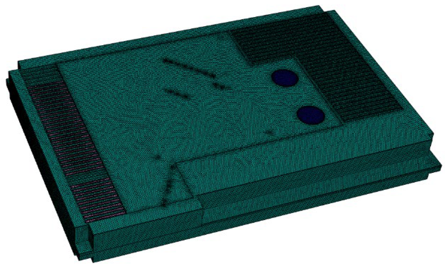
After meeting the above standards, the specific results of meshing are shown in Figure 4.

2.2.3. Solution Settings and Convergence Criteria

A sequential coupling solution strategy is adopted, where the thermal field is solved first, and then its results are input into the mechanical field as loads. The specific numerical methods are as follows:
First, the thermal field is solved using Ansys Fluent 2022 R1 software. The energy equation is enabled, and the standard k-ε turbulence model is selected to balance computational efficiency and potential turbulent mixing effects in the enclosed space (with Reynolds number Re > 2300). Next, material properties and boundary conditions are set. Since fully enclosed ruggedized computers typically operate in a long-term continuous working mode, the internal temperature field stabilizes after a period of operation. Moreover, compared with transient solutions that require 1200 time steps, the computational time is reduced by 95%, so the steady-state solution is adopted. The ambient temperature is set to gradient working conditions of 25–55 °C. Through multi-condition comparison, the environmental adaptability of the thermal design is verified, and the heat dissipation margin under different environments is evaluated.
In the residual convergence criteria, the continuity equation is set to 1 × 10 3 , and the energy equation set to 1 × 10 6 to ensure stable convergence of the solution. For physical quantity convergence, the temperature of core components (such as chip 3A6000) is monitored. Convergence is determined when the temperature change is less than 0.1 °C for 50 consecutive iterations.
Subsequently, the mechanical field is solved using the Finite Element Method (FEM), with the element type being solid elements (SOLID186) that support thermal-structural coupling. The temperature field solved by Fluent is imported via the “load transfer” function as a thermal strain load. Vibration/shock loads are applied according to experimental standards (e.g., random vibration acceleration of 10 g, shock acceleration of 20 g). A sparse matrix solver (PCG solver) is used for the solution.
The convergence criterion for the mechanical field is defined as follows: force balance convergence is achieved when the unbalanced force ratio is determined to be less than 1 × 10 5 . For the displacement convergence criterion, the maximum deformation of the PCB is monitored, and convergence is determined when the deformation change is less than 1.0 × 10 6 mm for 20 consecutive iterations.

2.2.4. Analysis of Temperature Field Results

After the solution settings, this paper conducts a temperature field simulation analysis of the fully enclosed ruggedized computer. It focuses on analyzing its temperature distribution in the 25–55 °C operating environment, with the analysis content including three parts. The first part is core components, including Chip 3A6000, Chip 7A2000, Chip X100, DDR4 memory, Chip 1860, Chip 2329, and Chip a200. The second part is heat-dissipating heat pipes, mainly the heat pipes for Chip 3A6000, Chip 7A2000, and Chip X100. The third part is system temperature uniformity, including the average temperature of the PCB, the chassis shell, and the air domain inside the chassis. In the measurement of temperature, taking the average temperature of the PCB as an example, the specific steps are as follows:
(1)
Enter the “Surface” panel and select “Zone Surfaces”.
(2)
From the drop-down menu, select the solid domain of the PCB (e.g., “PCB_Solid”) to generate the “volume region” of the PCB.
(3)
Enter the “Reports > Surface Integrals” panel.
(4)
For the calculation type, select “Volume-Weighted Average”; for the integrand variable, select “Temperature” (temperature).
(5)
Click “Compute”. Fluent will automatically calculate the average temperature of this region, i.e., the average temperature of the PCB.
Through the analysis of the temperature variation trends of core components, it can be directly observed whether they meet the operating requirements and the coupling effects between heat sources. Through the analysis of system temperature uniformity, the stability of the system’s thermal balance can be evaluated.
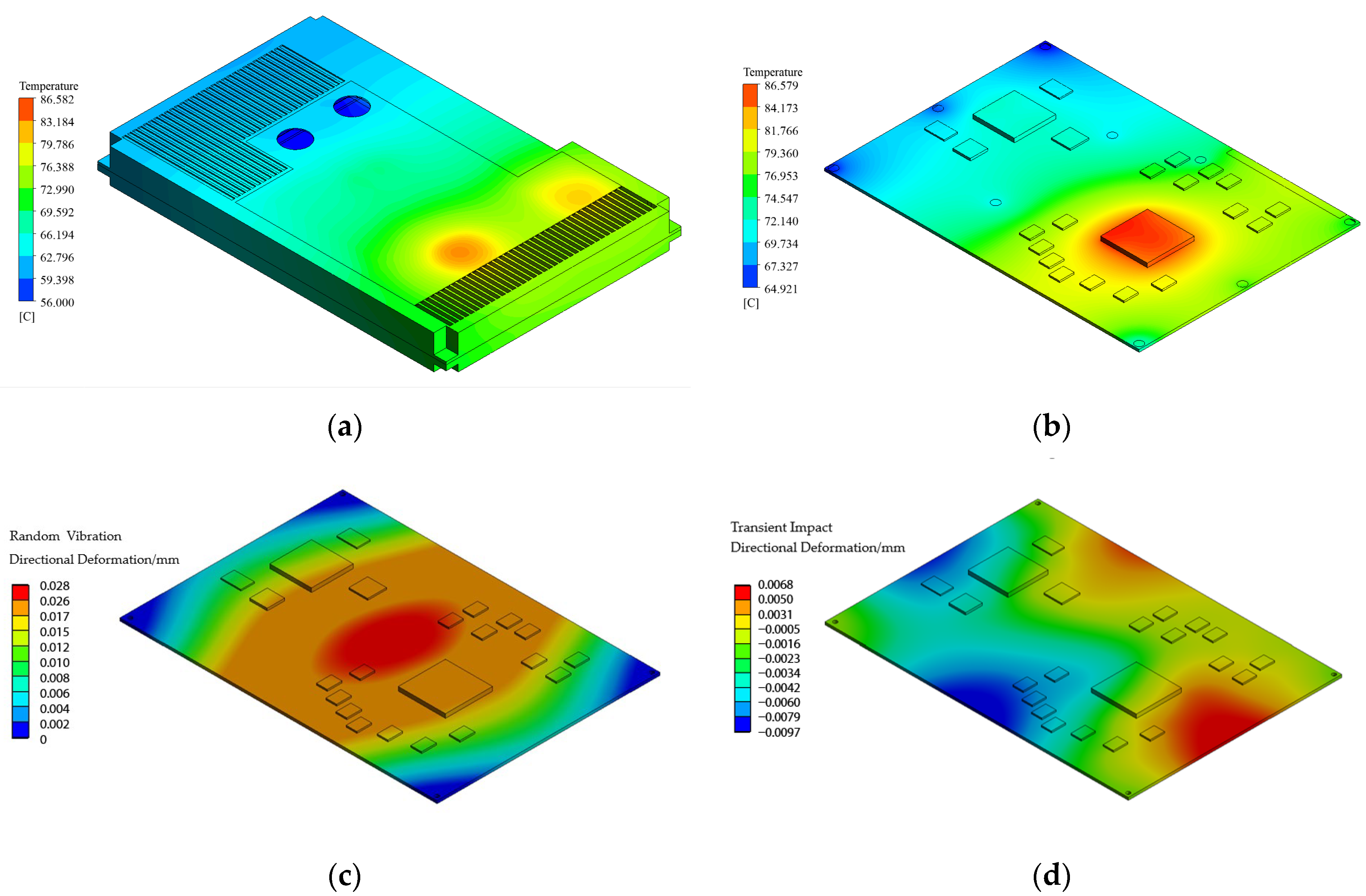
Figure 5 shows the simulation results of the initial chassis before optimization. It can be seen from Figure 5a,b that when the ambient temperature reaches 55 °C, the temperature of the 3A6000 chip rises to 91.1 °C, the 7A2000 chip to 86.9 °C, the X100 chip to 79.1 °C, and the DDR4 memory to 87.7 °C; the temperatures of the 1860 chip, 2329 chip, and a200 chip are 74.1 °C, 74.1 °C, and 80.3 °C, respectively. By referring to the device data sheets, it is found that the 3A6000 chip, 7A2000 chip, DDR4 memory, and X100 chip do not meet their allowable temperature requirements. Therefore, it is necessary to carry out heat dissipation optimization design for the fully enclosed ruggedized computer.
As shown in Figure 5c,d, regarding the temperature difference range between the evaporating section and the condensing section of the heat pipes, the temperature differences in the three heat pipes are all within 5–20 °C, indicating that they are all in the optimal working state. It can be seen that the design of the heat pipe cooling system is reasonable.

3. Methods

Based on the temperature field simulation results of the fully enclosed ruggedized computer under an ambient temperature range of 25–55 °C in Section 2, it is found that when the ambient temperature reaches 55 °C, the heat flow coupling effect between compactly arranged components is significant. This section addresses this issue by conducting thermal optimization design from both board-level and system-level perspectives. Firstly, the ant colony algorithm is improved to propose the P-MMAS algorithm, which is used to optimize the layout of board-level components. Secondly, without considering the layout of board-level components, the orthogonal test method is applied to optimize the layout of each module inside the chassis.

3.1. PCB Layout Optimization Strategies

For the PCB layout optimization method, an improved strategy based on the P-MMAS algorithm is adopted. The P-MMAS algorithm is a new multi-objective ant colony algorithm proposed on the basis of the MMAS algorithm by redesigning the dynamic state transition strategy, hybrid local search strategy, and multi-objective pheromone update strategy, while introducing the Pareto solution set. Its core idea is to combine the Pareto optimal frontier theory with the pheromone control mechanism of MMAS, aiming to approximate the Pareto optimal solution set of multi-objective optimization while ensuring the diversity of the solution set.

3.1.1. Dynamic State Transition Strategy

By defining dynamic weights λ t , the target focus can be adjusted according to the current temperature distribution. Compared with fixed weights, which cannot dynamically respond to local hotspots in the layout or thermal stress concentration, leading to a single and rigid optimization direction, the introduction of dynamic weights can independently adjust conflicts between targets and avoid falling into local optimization of a single target. The dynamic weights are set based on the ratio of average temperature to stress:
λ ( t ) = σ temp   ( t ) σ temp   ( t ) + σ stress   ( t )  
In the formula, σ temp   ( t ) represents temperature variance, σ stress   ( t ) represents stress variance, and t denotes the iteration number.
In each iteration, the set m ants plan their travel paths according to the dynamic state transition strategy. This paper adopts the dynamic state transition strategy based on the pseudo-random proportion rule with dynamic weights to determine the next traveling node:
s = arg max j Ω τ temp , i j λ α τ stress , i j ( 1 λ ) α η i j β , q q 0 , S , other
In the formula, α is the parameter controlling the proportion of pheromones, and β is the parameter controlling the weight of the heuristic factor, usually with α = 1 and β = 1 ; q is a random number within the interval [0, 1]; q 0 is a constant, generally taking the value q 0 = 0.98 . When q q 0 , it tends to exploitation, that is, selecting the current optimal combination; when q > q 0 , it explores according to probability S to avoid premature convergence; Ω represents the feasible region of the node; τ temp , i j and τ stress , i j respectively denote the pheromone concentrations of temperature and stress from position i to position j , where i is the grid position of the current component and j is the next planned grid position to be selected; n i j represents the heuristic factor from position i to position j , specifically:
η i j = 1 d temp , i j + d stress , i j
In the formula, d temp , i j represents the expected temperature rise, and d stress , i j represents stress sensitivity. S can be expressed by the dynamic state transition probability:
P i j ( t ) = τ temp , i j ( t ) λ α τ stress , i j ( t ) ( 1 λ ) α η i j β k Ω τ temp , i k ( t ) λ α τ stress , i k ( t ) ( 1 λ ) α η i k β , j Ω , 0 , other  

3.1.2. Hybrid Local Search Strategy

To address the special constraint of physical coupling in component layout on the PCB of fully enclosed ruggedized computers, this paper proposes a hybrid local search strategy combining Thermal-Driven Swap and Stress Gradient Adjustment. The core logic of TDS is to screen high-temperature and low-temperature components and directly reduce local temperature by swapping their positions. The core logic of SGA is to calculate the stress gradient of high-stress components and move them along the gradient descent direction. For high-temperature and high-stress units that have been frequently adjusted recently, the tabu list idea is introduced to prevent local search stagnation and cyclic oscillations. The integration with tabu search improves the diversity of the search while avoiding infinite loops.

3.1.3. Multi-Objective Pheromone Update Strategy

For the component layout optimization of component layout on PCB in fully enclosed ruggedized computers, considering potential conflicts between temperature and stress objectives, independent pheromone matrices are adopted to avoid mutual interference between the two objectives, enhancing the algorithm’s search specificity.
In each iteration, P-MMAS generates multiple Pareto fronts. To search these fronts for better solutions, based on the positive feedback principle of ant colony algorithms, pheromones are updated by attenuating old concentrations with volatility rate ρ and superimposing the latest solutions from current Pareto fronts. The temperature pheromone update follows the formula:
τ temp , i j ( t + 1 ) = ( 1 ρ ) τ temp , i j ( t ) + k = 1 m Δ τ temp , i j k τ max
The specific iteration rule of temperature pheromones is that after the current concentration is volatilized at the volatilization rate ρ , the contributions Δ τ temp , i j k of all ants on path i , j are superimposed, and the pheromones are truncated within the range of τ min , τ max . In the formula, τ temp , i j ( t ) represents the concentration of temperature pheromone from position i to j in the t -th iteration; ρ represents the pheromone volatilization rate, which is used to control the volatilization rate of old pheromones; Δ τ temp , i j k represents the contribution of the k -th ant to the temperature pheromone on path i , j , and the specific expression method is as follows:
Δ τ temp , i j k = Q f t e m p ( k ) I i , j P a r e t o
In the formula, Q is the pheromone intensity constant, with a value of 1 here; f t e m p ( k ) represents the temperature objective function value of the k -th solution; I i , j P a r e t o is an indicator function, which takes a value of 1 if the path i , j belongs to the current Pareto frontier solution, otherwise 0.
The update of stress pheromones is completely symmetric to the update formula of temperature pheromones, and the specific formula is as follows:
τ stress , i j ( t + 1 ) = ( 1 ρ ) τ stress , i j ( t ) + k = 1 m Δ τ stress , i j k τ max
Δ τ stress , i j k = Q f stress ( k ) I { ( i , j ) Parcto }
In the update formulas of temperature and stress pheromones, the mentioned τ min and τ max respectively represent the lower and upper limits of pheromone concentration, and the pheromone truncation operator x a b is defined as:
x a b = a , x < a b , x > b x , o t h e r
The expressions for the upper and lower limits of pheromone concentration are as follows:
τ max = 1 ρ f min
τ min = τ max max F a c t o r
In the formula, f min is the optimal objective function value among all current solutions. Here, normalization is used to eliminate the dimensional difference between different objectives of temperature and stress. max F a c t o r is the upper and lower limit scaling factor, which is usually set to 5. When the pseudo-random proportional rule is selected as the state transition strategy, the pheromone concentration interval should be chosen to be relatively narrow for better results.

3.1.4. Pareto Solution Set Update Strategy

To maintain the diversity of optimal solutions without compromising convergence speed, the Pareto solution set update strategy is addressed through the synergy of three aspects: adaptive grid maintenance, elite solution reward, and dynamic storage expansion.
Adaptive grids enforce uniform distribution of solutions in the objective space, avoiding local aggregation and maintaining solution diversity. Compared with traditional niche algorithms, they have lower complexity and faster convergence. In this paper, the adaptive grid maintenance formulas mainly include two parts: grid division and solution distribution regulation:
K = N a r c h i v e
In the formula, N a r c h i v e is the number of solutions in the current archive, and K represents the grid division dimension of the objective space, which can be dynamically adjusted according to the number of archived solutions.
θ = N a r c h i v e K 2
In the formula, θ represents the maximum allowable threshold of the number of solutions in a single grid. If the number of solutions in the grid exceeds θ , the excess solutions will be deleted randomly.
The elite solution reward mechanism enables solutions with better objective values to obtain double pheromone rewards, strengthens their search guidance role, and accelerates the convergence speed. For the selection of elite solutions, it is first necessary to normalize the objective values to eliminate dimensional differences. The specific formula is as follows:
f temp k = f t e m p k f t e m p , max
f s t r e s s k = f s t r e s s k f s t r e s s , max
The comprehensive score is calculated in a weighted manner to sort and compare the solution sets, and the top N e l i t e solutions are selected according to the ranking. In this paper, the top 10% of the Pareto frontier is taken.
For the selected elite solutions, the reward mechanism is implemented:
Δ τ e l i t e , i j = 2 Q f t e m p k + f s t r e s s k
In the formula, f t e m p k and f s t r e s s k represent the temperature and stress objective values of the K-th solution, respectively; Q is a pheromone intensity constant, which is set to 1 in this paper.
The adjustment of the dynamic archive size is based on the archive expansion cycle. After specifying the capacity of each expansion, the archive will be dynamically expanded whenever the corresponding number of iterations is reached. While optimizing and exploiting, more exploration possibilities are retained. Its specific implementation is as follows:
N a r c h i v e t = N a r c h i v e i n i t + t T g r o w Δ N
In the formula, N a r c h i v e i n i t is the initial archive capacity; T g r o w is the archive expansion cycle; Δ N is the increment of each archive expansion.

3.2. Analysis of PCB Layout Optimization Case Studies

First, problem modeling is conducted. The PCB board in a fully enclosed ruggedized computer contains a large number of components with varying sizes. Therefore, simplification is essential before constructing the solution model.
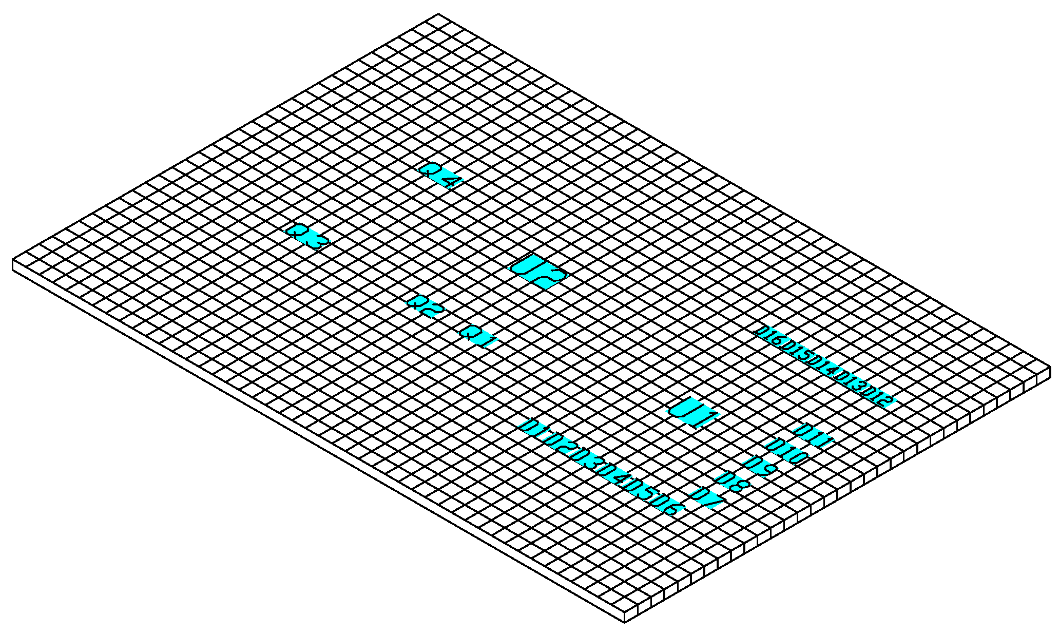
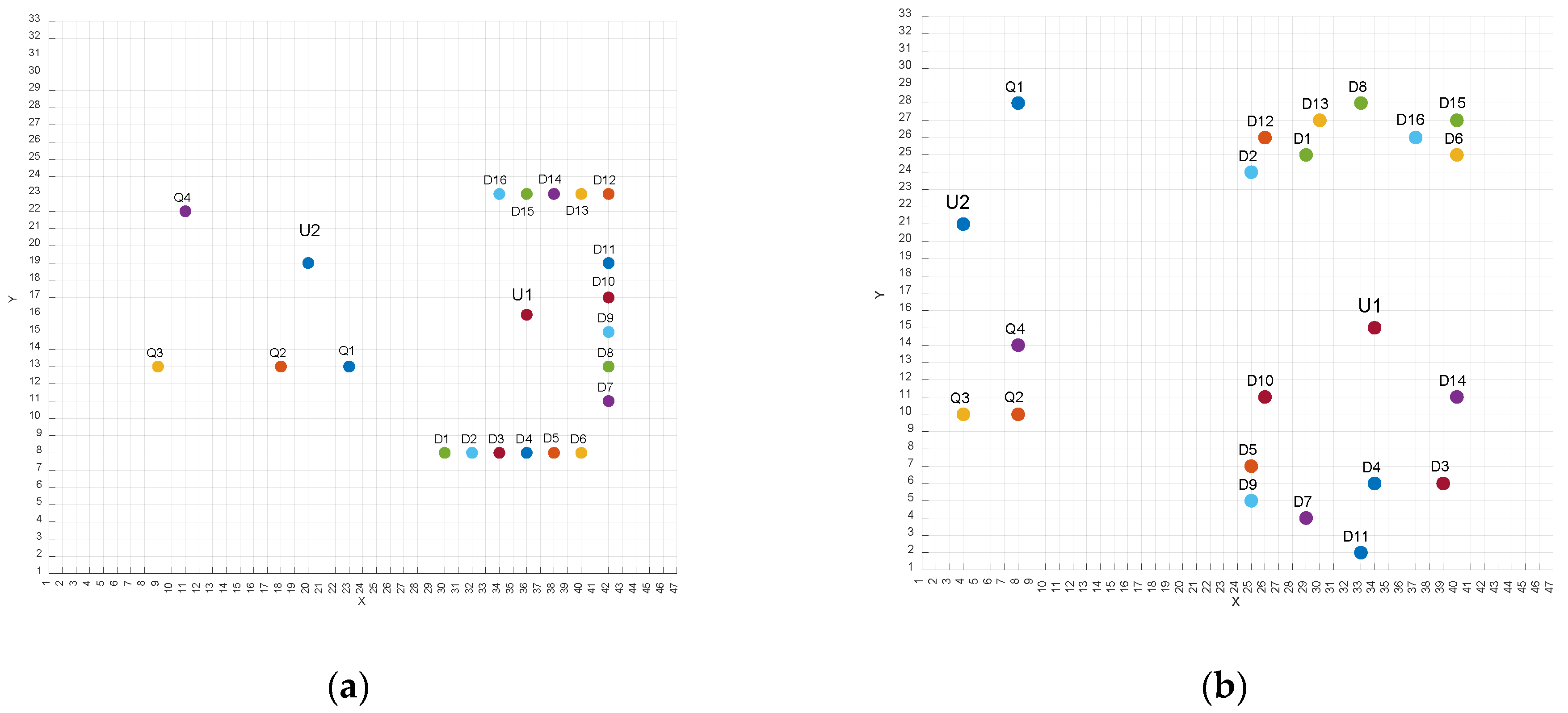
For the PCB board, using the smallest component size on the PCB as the unit dimension, the PCB is divided into a 46 × 32 uniform rectangular grid, as shown in Figure 6. Here, the row numbers from bottom to top are denoted as i = (1, 2, …, 31, 32), and the column numbers from left to right are denoted as j = (1, 2, …, 45, 46). The coding is performed in row-major order, where each grid node coordinate i , j corresponds to a unique grid position number P i j .
For the components, the power chips and memory from the simulation are retained and equivalent to power modules with dimensions consistent with the unit size. The equivalent power consumption of each power module is the product of its heat flux density and the volume of the equivalent module. Each power module is assigned a distinct reference designator based on its chip type; for instance, the chip 3A6000 is designated as U1, and the DDR4 memory modules are designated as Q1 to Q16. The specific position of a component on the PCB can be determined by the number of the unit closest to the center of the component. A set of known components can be constructed as C = C 1 , C 2 , C k , where each component C k is associated with its fixed basic parameters, including reference designator, power consumption, thermal conductivity, and mass. The position number, i.e., coordinate information, is set as an independent attribute that can be updated during algorithm iteration. The relationship between the initial component reference designators and the PCB position numbers is presented in Table 4.
Among them, Q1 and Q2 are chip 1860, Q3 is chip a200, Q4 is chip 2329, D1–D16 are memory DDR4, U1 is chip 3A6000, and U2 is chip X100.

3.2.1. Solution Process

The layout optimization of PCB components in a fully enclosed ruggedized computer based on the P-MMAS algorithm follows the specific process as below: First, set the basic parameters of the ant colony (such as the number of ants, pheromone concentration, evaporation coefficient, etc.). Then, carry out path construction selection and pheromone update through an iterative process, and judge whether the currently obtained solution meets the optimization target or the requirements of the Pareto frontier. If the conditions are met, the algorithm terminates and returns the optimal solution; otherwise, it continues path selection and pheromone update until the predetermined number of iterations or convergence conditions are reached. Finally, the algorithm can output a set of non-dominated solutions, i.e., Pareto optimal solutions, which represent the best balance among objectives such as heat dissipation, vibration, and impact.

3.2.2. Definition of Relevant Variables

For the layout optimization of PCB components in a fully enclosed ruggedized computer, the maximum temperature of the PCB board T max , the maximum temperature difference between PCB boards Δ T , and the maximum deformation of the PCB board d max are taken as the objective functions. Each component layout sequence corresponds to a layout scheme, with the layout positions of components as constraint conditions.
In the optimization process, if only minimizing T max is pursued, high-power chips will be centrally arranged near heat pipes, leading to an increase in local Δ T . If only minimizing Δ T is prioritized, high-power chips need to be dispersed, which will move them away from heat pipes and result in a rise in T max . If only minimizing d max is targeted (to reduce thermal stress concentration), the optimal heat dissipation positions for high-power chips will be restricted, causing both T max and Δ T to deteriorate simultaneously. Without referencing the Pareto solution set, five groups of solutions were extracted, and the simulation comparison results are shown in Table 5:
Each component layout sequence corresponds to a specific layout scheme, with the components’ placement positions serving as constraint conditions. The PCB dimensions are 230 mm × 160 mm, and the components’ placement must satisfy five conditions:
(1)
The spacing between components must be at least 2 mm, complying with soldering process requirements.
(2)
The distance between high-power chips and heat pipe contact points must not exceed 5 mm to ensure heat conduction efficiency.
(3)
The connection length between Chip 3A6000 and DDR4 must not exceed 50 mm, while their spacing must be at least 5 mm—this maintains signal integrity and prevents thermal coupling.
(4)
The contact area between heat pipes and high heat flux density chips (Chip 3A6000 and Chip 7A2000) must be greater than 70% of the component base area to meet heat dissipation demands.
(5)
A 10 mm reserved area for bolt fixing must be maintained along the PCB edges.
In summary, the optimization problem for component layout on the PCB is as follows:
min T max = f 1 P - M M A S C k , i , j   Δ T = f 2 P - M M A S C k , i , j   d max = f 3 P - M M A S C k , i , j       s . t .   1 i 32 1 j 46 I f   C k   o c c u p i e s   t h e   p o s i t i o n ( i , j ) ,   t h e n     C m     C k
The variables in the solution process are defined as follows: After meshing, the length of the unit node in the y-direction ( Δ y ) is 5 mm, the length in the x-direction ( Δ x ) is 5 mm, and the height ( h ) of the unit node is 2 mm. The equivalent thermal conductivity of the PCB is 30 W / m K . The ambient temperature (t0) is 55 °C. The equivalent density of the PCB ( ρ p c b ) is 1870 k g / m 3 . The equivalent elastic modulus of the PCB ( E p c b ) is 6.82 × 10 9 Pa. The equivalent Poisson’s ratio of the PCB ( υ p c b ) is 0.3. The equivalent density of the component module ( ρ d e v ) is 1800 k g / m 3 . The equivalent elastic modulus of the component module ( E d e v ) is 2.76 × 10 10 Pa. The equivalent Poisson’s ratio of the component module ( υ d e v ) is 0.3 [30].

3.2.3. PCB Layout Optimization Results

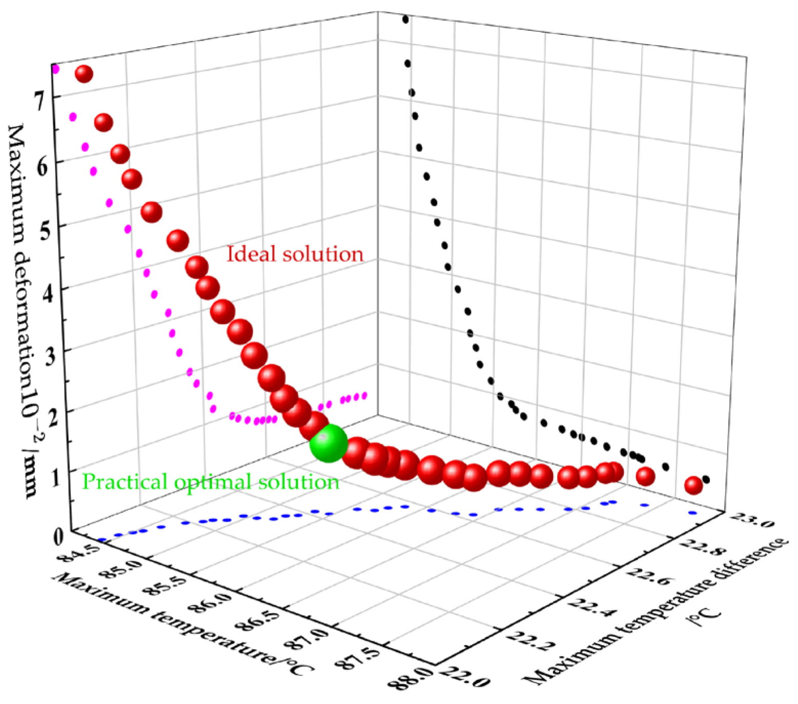
To address the issue of thermal coupling effects caused by the compact layout of high-power components in fully enclosed ruggedized computers under high-temperature environments, in the optimization calculation, the ambient temperature is set to 55 °C. The code is written using MATLAB R2022b, with the number of ants set to 30, the pheromone weight to 1, the heuristic factor weight to 2, the volatility rate to 0.1, max F a c t o r valued at 5, and the number of iterations ( T max ) set to 800. By performing the objective optimization of the P-MMAS algorithm, the Pareto frontier solution set and its projections on each plane can be obtained, as shown in Figure 7. The Pareto frontier solution set is set to consist of 90 Pareto optimal solutions.
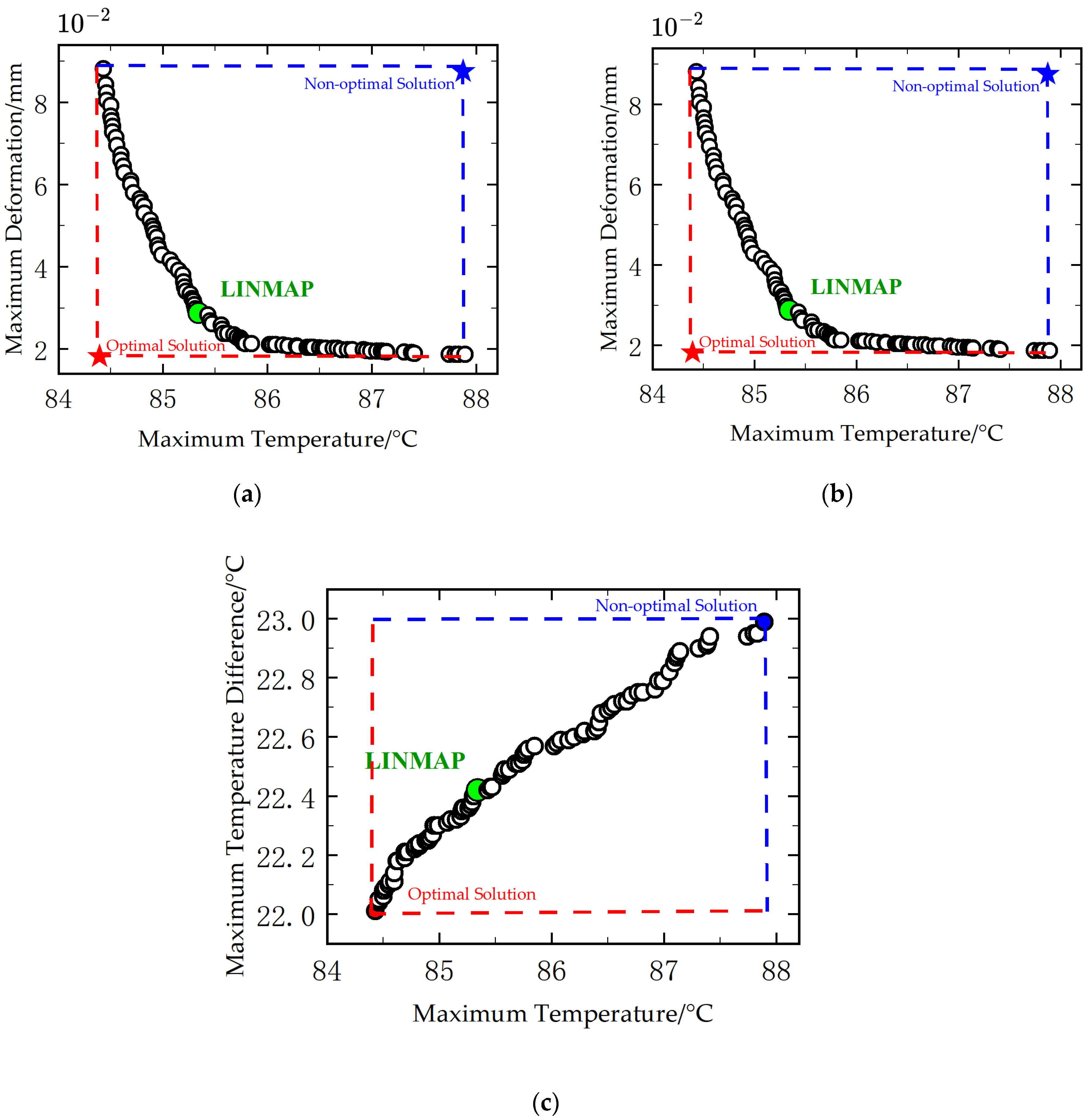
Figure 8 is the Pareto frontier distribution map in the two-dimensional coordinates corresponding to Figure 3. This paper adopts the classic LINMAP decision-making method to select the optimal solution from the Pareto frontier solution set. The figure depicts the ideal solution, the non-ideal solution, and the classic solution selected by the LINMAP decision-making method, respectively.
As can be seen from Figure 8a, the two-dimensional Pareto frontier distribution map with the maximum temperature and maximum deformation displacement of the PCB board as the objective functions, there is a negative correlation and an approximately inverse proportional relationship between the maximum temperature of the PCB board and the maximum deformation displacement. As the temperature of the PCB board gradually increases, its deformation displacement gradually decreases. The two objective functions restrict each other, and the optimal solution selected according to the LINMAP decision-making method has been indicated in the figure. Figure 8b is a two-dimensional Pareto frontier graph with the maximum temperature difference between PCB boards and the maximum deformation displacement as the objective functions. It can be seen from the figure that as the maximum deformation displacement of the PCB board decreases, the maximum temperature difference gradually increases, and with the progress of iterations, as the maximum deformation displacement decreases, the growth rate of the maximum temperature difference accelerates. Figure 8c is a two-dimensional Pareto frontier graph with the maximum temperature of the PCB board and the maximum temperature difference between PCB boards as the objective functions. It can be seen from the figure that the two are positively correlated, and the ideal solution is the minimum value of both.
According to the optimal solution selected by the LINMAP decision-making method, the final layout result of its components is shown in Figure 9, and the specific component reference designators and position coordinate numbers are listed in Table 6.
Based on the component layout information obtained from the optimal solution selected by the LINMAP decision-making method, the model of the fully enclosed ruggedized computer is reconstructed and thermodynamic simulation is carried out.

3.3. Comparative Analysis of Simulation Results for the Optimized PCB

A simulation model was reconstructed based on the optimized component layout. The ambient temperature was set to 55 °C, and other boundary conditions remained consistent with those before optimization. A thermal simulation analysis was conducted, and the simulation results of the chassis shell and PCB board after reaching a stable state are shown in Figure 10.
The first part compares the optimal solution selected by the LINMAP decision-making method with the results of the actual simulation model, and the comparison results are shown in Table 7. It can be seen that the maximum temperature of the PCB, the temperature difference between PCBs, and the maximum deformation between PCBs obtained from the selected optimal solution are consistent with the results of the actual simulation model, with the maximum relative error not exceeding 3.5%, which further illustrates the accuracy of the P-MMAS optimization algorithm.
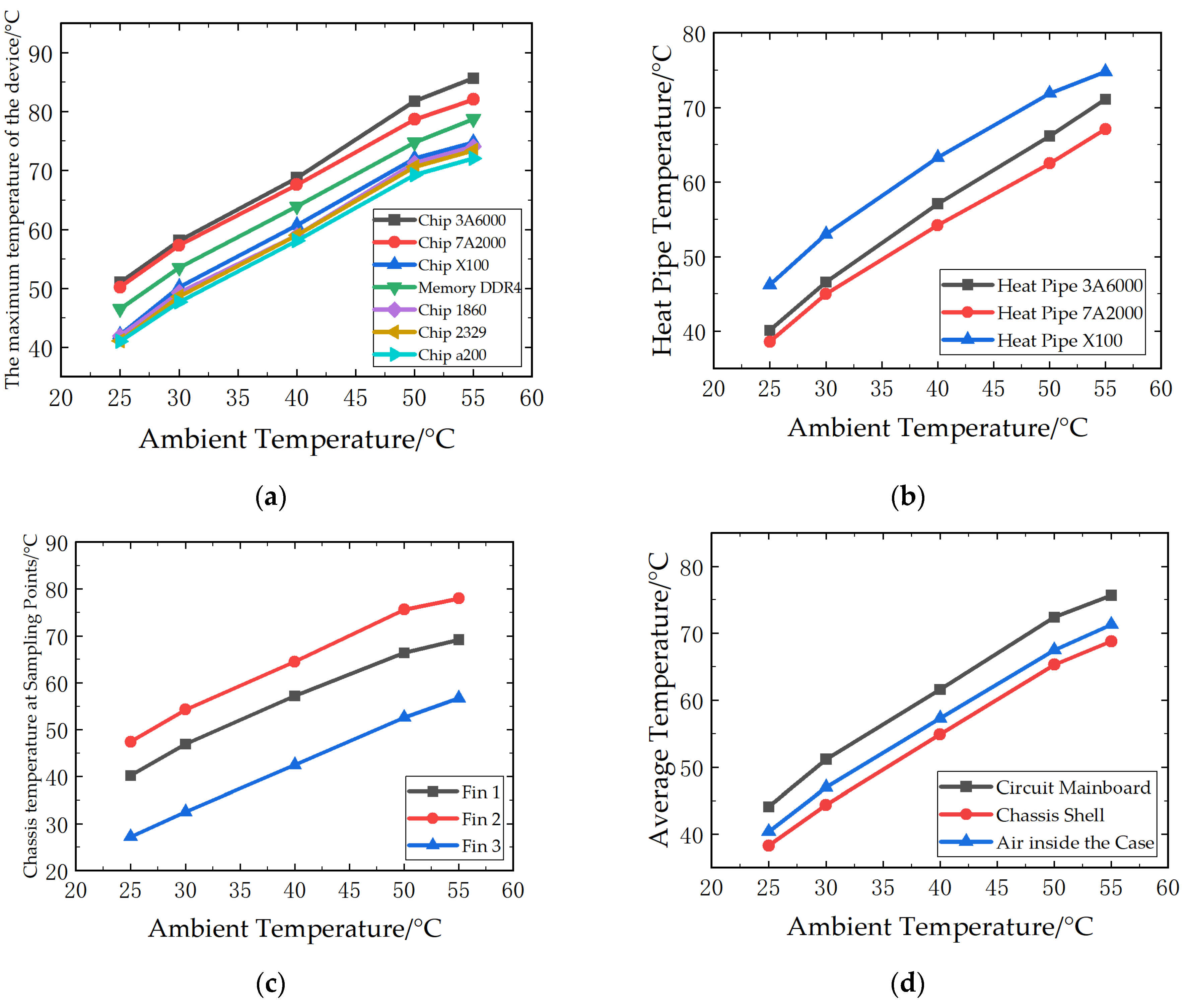
In the second part, thermal simulations were conducted on the optimized model under different ambient temperature gradients. The steady-state temperature change curves for the four modules, namely core components, heat-dissipating heat pipes, chassis shell fins, and overall temperature uniformity, are shown in Figure 11. It can be seen from Figure 11a that as the ambient temperature increases, the temperature of each chip also rises gradually. When the ambient temperature is 55 °C, the maximum temperature of chip 3A6000 is 86.579 °C, chip 7A2000 is 82.1 °C, chip X100 is 74.8 °C, memory DDR4 is 78.8 °C, chip 1860 is 74.1 °C, chip 2329 is 73.4 °C, and chip a200 is 72.1 °C. All chips meet their allowable temperature requirements, which further verifies the effectiveness of the optimization. Figure 11b shows the maximum temperature at the condensation end of the heat pipes. The temperature differences between the evaporation end and condensation end of the heat pipes for chip 3A6000, chip 7A2000, and chip X100 are 19.479 °C, 7.3 °C, and 5.6 °C, respectively. All temperature differences are within the range of 5~20 °C, indicating that the heat pipes are in optimal performance. It can be seen from Figure 11c that the temperature of fin 2 is much higher than that of other fin collection points. Through the simulation model, it is found that chip 7A2000 is placed on a separate PCB board and does not participate in the layout optimization of components on the main control PCB board. Its position remains the same as before optimization and is not directly connected to the fan flow channel, hence the higher temperature. Figure 11d presents the average temperatures of three components: the chassis shell, the air inside the chassis, and the PCB motherboard. Specifically, the average temperature of the chassis shell is 68.8 °C, the average temperature of the internal air is 71.3 °C, and the average temperature of the PCB motherboard is 75.7 °C. Notably, the average temperature of the PCB is below 80 °C, which reduces the risk of PCB deformation caused by thermal stress.
The third part compares the maximum temperature of each chip and the average temperature of the PCB board at an ambient temperature of 55 °C before and after optimization, with details shown in Table 8. It can be seen from the table that after optimizing the layout of components on the PCB board, under the same working conditions, the maximum temperatures reached by chip 3A6000, chip 7A2000, and chip X100 during operation all decreased by approximately 5 °C. The 16 memory particles, which changed from a compact layout before optimization to a scattered layout after optimization, saw their temperatures all drop by about 10 °C, reducing the impact of the thermocouple effect caused by the compact layout of components.
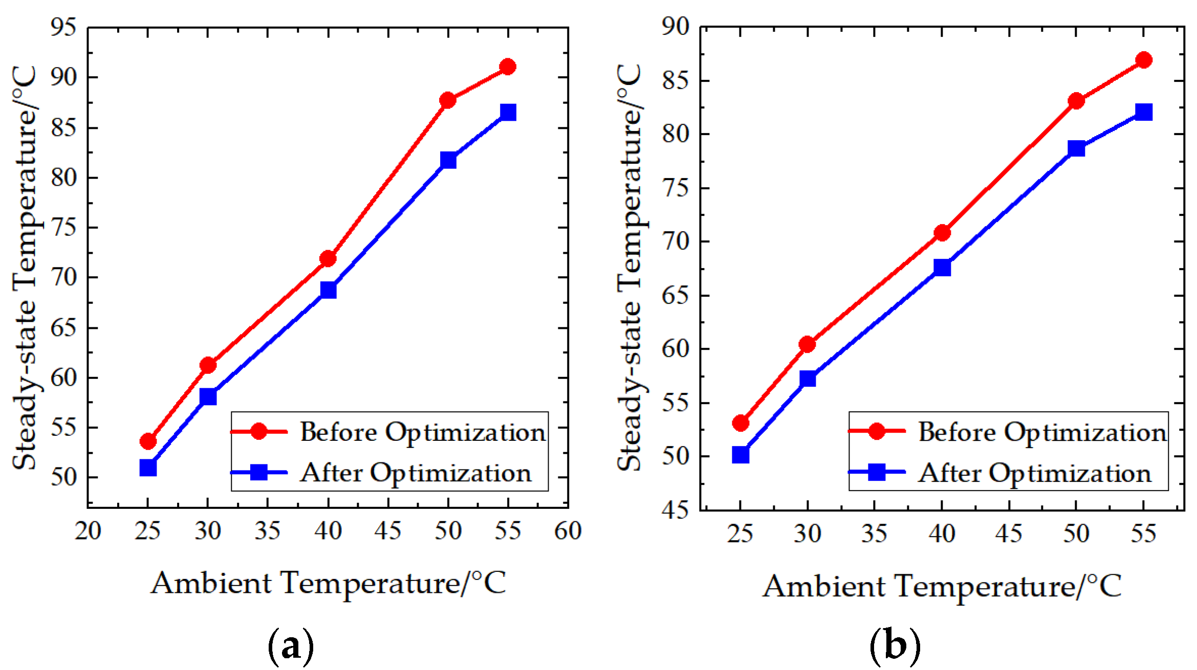
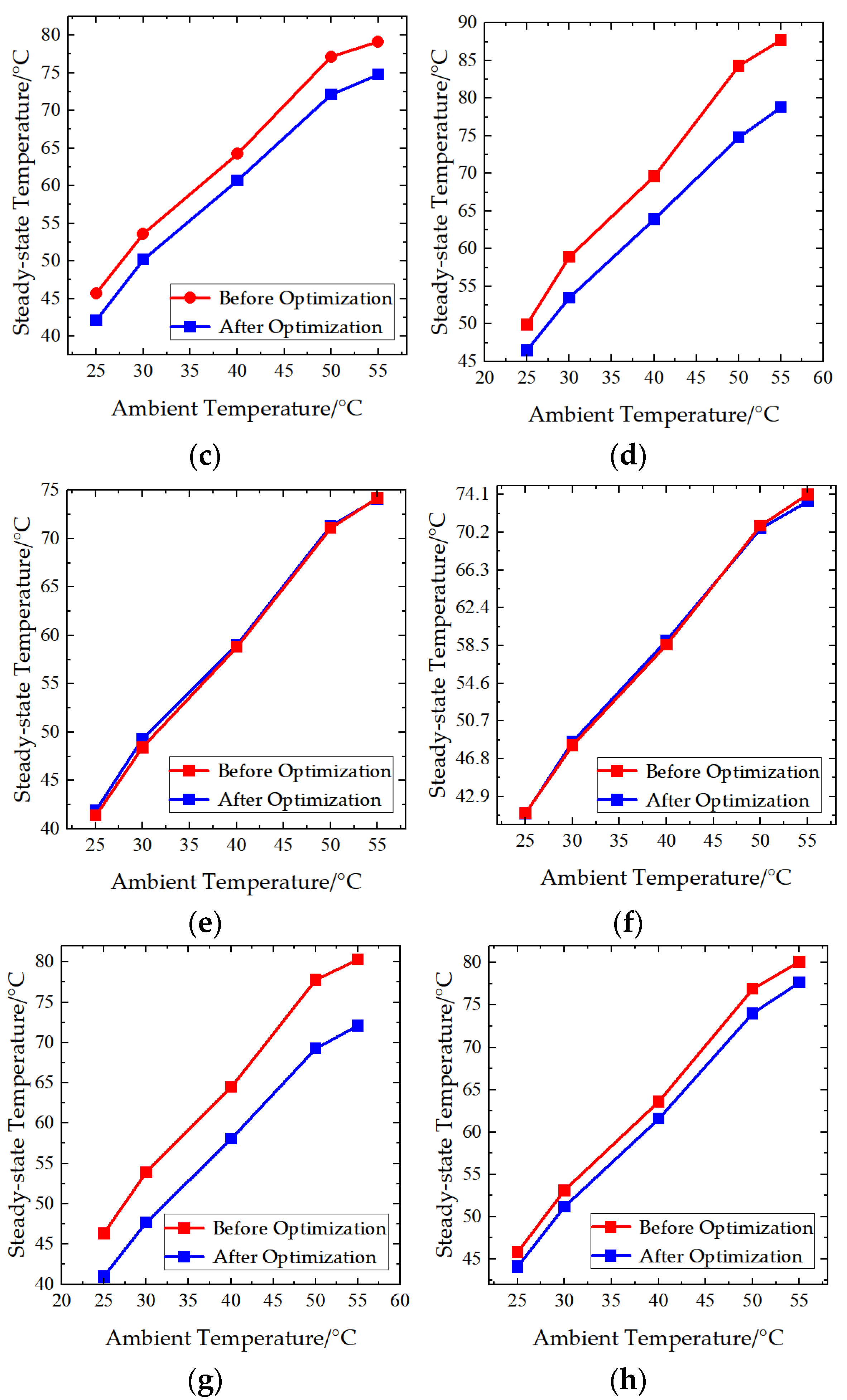
Figure 12 shows the maximum temperatures of chips and various components at steady state under different ambient temperatures, both before and after optimization. It can be seen from Figure 9 that the steady-state temperatures of all power chips after optimization are significantly lower than those before optimization. The temperatures of Chip 2329 and Chip a200 remain basically consistent under different ambient temperatures both before and after optimization. From the simulation diagrams, it can be observed that these two chips are far away from other chips both before and after optimization, resulting in low local thermal coupling effects between them and other chips. This further indicates that through the layout optimization of components, the impact of abnormal temperature rise caused by thermal coupling effects between chips can be significantly reduced. In addition, both the average temperature of the PCB board and the average temperature of the chassis shell decrease significantly after optimization, which shows that the heat dissipation performance of the entire system can be improved through the layout optimization of components.

3.4. Analysis of Module Layout Optimization Inside the Chassis

Following the completion of PCB layout optimization, this section continues to investigate the module layout optimization of fully enclosed ruggedized computers, which falls under the category of constrained multi-variable optimization problems. The objective function is defined as the maximum temperature of each component, while the design variables include the layout position of the fan module inside the chassis and the physical dimensions of the fan itself.
The origin (0, 0, 0) is set at the bottom-left corner of the chassis, with the coordinate axes aligned to the chassis dimensions. The diameter of the fan’s air inlet ranges from 10 mm to 40 mm (corresponding to twice the fan radius), the width of the air outlet ranges from 3 mm to 15 mm, and the thickness of the fan ranges from 8 mm to 25 mm.
For installation, a rigid fixing structure is required: the fan must be bolted to the chassis shell to prevent displacement or malfunction caused by vibration. Additionally, a 24V DC turbofan is selected to match the power supply system of the entire machine, avoiding fan failures due to voltage incompatibility.
In this section, the orthogonal experimental design method is adopted for the optimal design of the module layout inside the chassis. Through the optimal design of the layout position of the fan module and its size, the maximum temperature of each power device is reduced, and the thermal coupling effect between devices is minimized, thereby enabling the equipment to meet the requirements of normal operation under different ambient temperatures.

3.4.1. Establishment of the Optimization Objective Function

For the modules inside a fully enclosed ruggedized computer, which include power supply modules, fan modules, control modules, and motherboard modules (among others), the number of modules is substantial. If each module were considered individually, it would be necessary to account for not only layout interference between modules but also their mutual assembly relationships, thereby complicating the optimization process.
The essence of optimizing the layout of modules within the chassis lies in evaluating the air flow intensity inside the chassis under different layouts. Thus, modules can be simplified: adjusting the fan layout corresponds to altering the positional relationships between different modules. Therefore, optimizing the layout of chassis-internal modules can be transformed into optimizing the layout of the fan module within the chassis.
Accordingly, this section focuses on optimizing parameters such as the spatial coordinates x , y , z and dimensions ( r ) of the fan module—under the conditions that the PCB component layout has already been optimized and the positions of other modules remain fixed—to obtain thermal simulation results.

3.4.2. Orthogonal Experimental Design

Orthogonal experimental design is a methodology for studying multi-factor and multi-level problems. It selects representative points from comprehensive experiments based on the principle of orthogonality, enabling the identification of the optimal combination of factors with the minimum number of experiments. This approach is of great significance for reducing research and development costs and shortening the R&D cycle.
The purpose of this section is to analyze the optimal layout position of the fan module using the comprehensive balance method of orthogonal experiments, based on the results obtained from the Ansys Fluent 2022 R1 thermal simulation software.
The specific objective of the experiments is to determine the optimal layout and size of the fan module inside the fully enclosed ruggedized computer. The evaluation indicators include the maximum temperatures of the main power devices (chip 3A6000, chip 7A2000, and chip X100) and the average temperature of the PCB board. The optimization parameters are the fan’s spatial coordinates x , y , z and its radius ( r ). In the optimization design, each factor affecting the fan layout is set with 5 levels, and the specific data are presented in Table 9. Since this orthogonal experiment involves 4 factors and 5 levels, an L 25 4 5 orthogonal array is adopted.

3.4.3. Orthogonal Experiment Analysis

Experiments were conducted in accordance with the level combinations specified for each trial number in the orthogonal array. Specifically, parametric simulation modeling was performed using Fluent. The ambient temperature was set within a gradient of 25–55 °C, and 55 °C was selected as the ambient temperature for the present study. The experimental results are presented in Table 10.
Two primary methods are employed for the analysis of orthogonal experimental data, namely range analysis and variance analysis. Range analysis features simplicity in calculation, intuitive representation, and ease of understanding. Taking the PCB temperature uniformity as the main objective, the range analysis results are presented in Table 11.
As shown in Table 11, the K value represents the sum of experimental data at a specific level for a given factor, and the Kavg value denotes the corresponding average. The optimal level refers to the level number corresponding to the optimal Kavg value of a factor. The R value is the range of the factor, calculated as the difference between the maximum and minimum Kavg values for that factor. The R values can be used to compare the significance of each factor on the experimental results.
By examining the magnitudes of the R values, the experimental results indicate that the vertical coordinate z is the most significant factor, exerting the greatest impact on the experimental outcomes. This is followed by the radius r factor, and finally the horizontal coordinate x and vertical coordinate y , which have equal influence. Thus, the order of significance of the four factors is: vertical coordinate z > radius r > horizontal coordinate x = vertical coordinate y .

3.5. Comparative Analysis of Simulation Results After Module Layout Optimization

Based on the optimization results obtained in Section 3.4, the following conclusions can be drawn: the optimal performance is achieved when the fan radius r is set to 20 mm, the X-coordinate to 20 mm, the Y-coordinate to 15 mm, and the Z-coordinate to 40 mm. The temperature field distribution of the optimized model was obtained via thermal simulation using Fluent software. A comparative analysis was conducted between the temperatures of the power components (Chip 3A6000, Chip 7A2000, Chip X100, and DDR4 memory) and the PCB in the original equipment, and those in the optimized equipment, under an ambient temperature of 55 °C. The detailed comparison results are presented in Table 12.
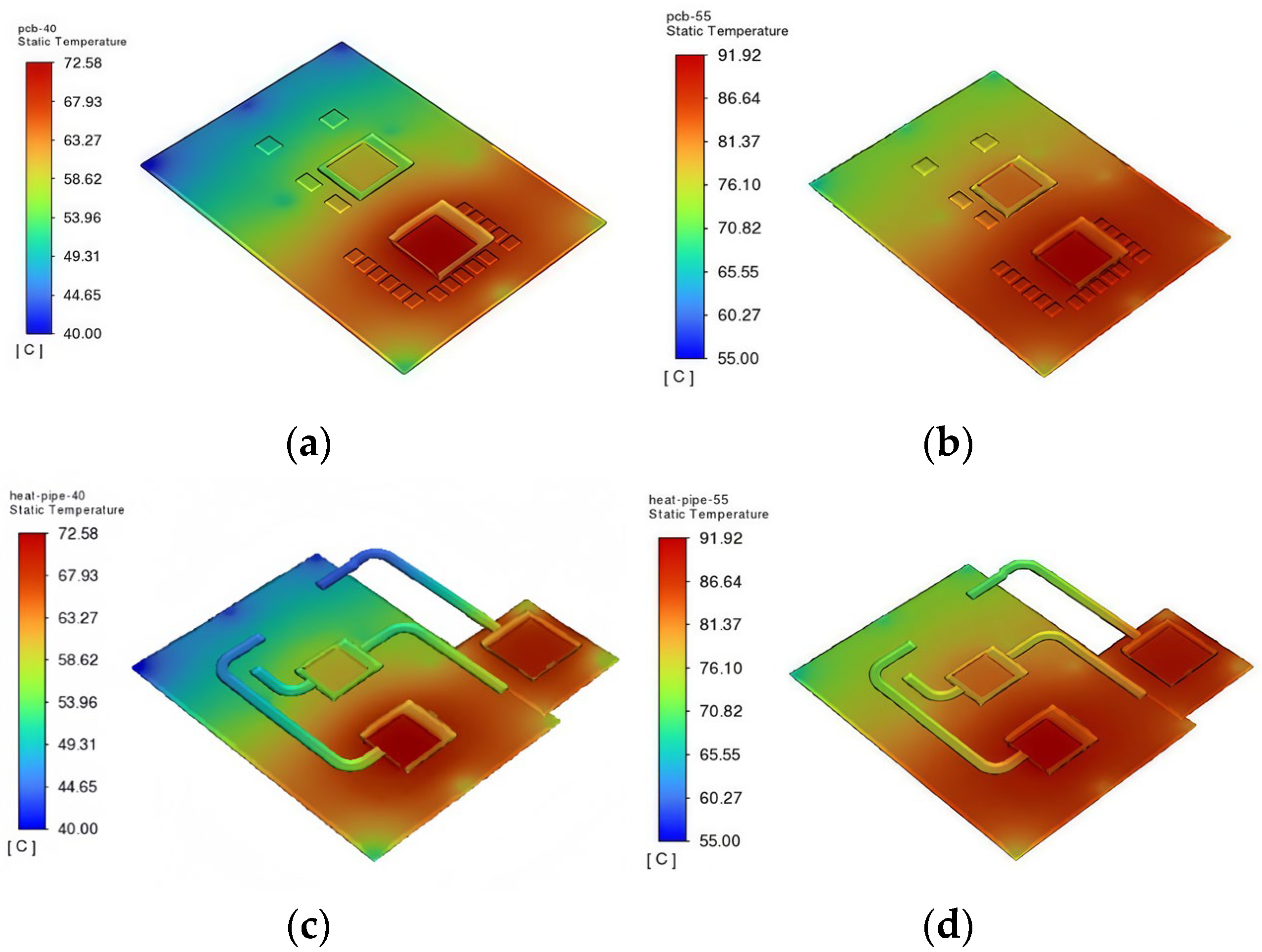
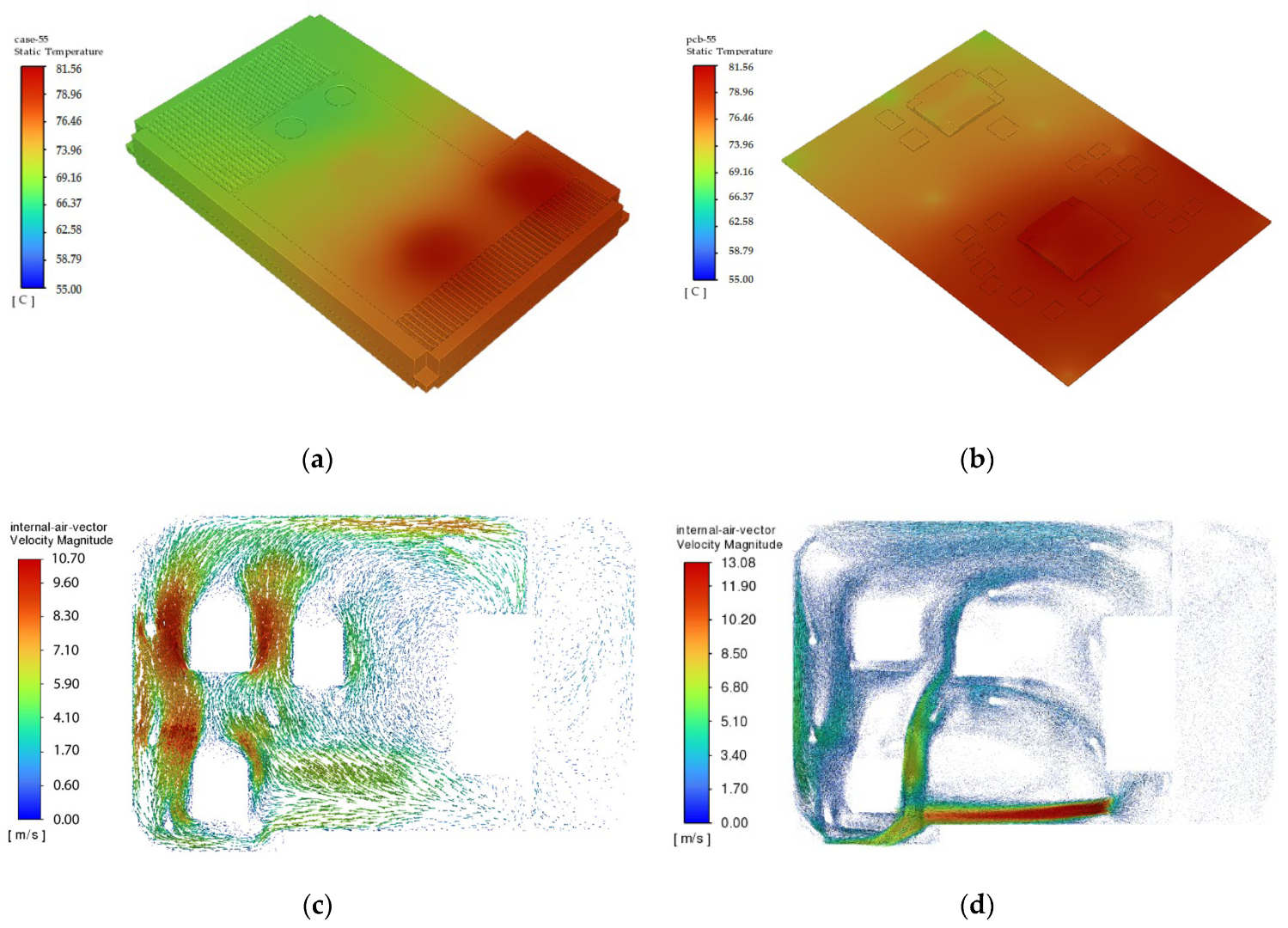
Analysis of the data in the table and Figure 13a,b show that the case temperature of Chip 3A6000 decreases from 91.1 °C to 81.6 °C; the case temperature of Chip 7A2000 decreases from 86.9 °C to 80.08 °C; the case temperature of Chip X100 decreases from 79.1 °C to 73.3 °C; the maximum internal temperature of the device decreases from 91.1 °C to 81.6 °C, a reduction of 9.5 °C; the average temperature of the PCB decreases from 80.1 °C to 73.1 °C; and the temperature of the chassis shell decreases from 73.0 °C to 67.9 °C. As can be seen from Figure 13c,d, the maximum air velocity inside the chassis has increased from 10.70 m/s to 13.08 m/s. This accelerates the heat transfer of locally dense components, reduces the thermal flow coupling effect between chips, and lowers the temperature of individual chips.
In summary, after two successive optimizations of the chassis, the maximum temperatures of the components are as follows: Chip 3A6000 reaches 81.56 °C, Chip 7A2000 reaches 80.80 °C, Chip X100 reaches 73.31 °C, and the memory reaches 77.63 °C. All these temperatures are within the allowable ranges, indicating that the optimized design meets the requirements. Additionally, the average temperature of the PCB is 73.12 °C, which reduces the risk of PCB warpage and deformation caused by thermal stress.

4. Experiment and Analysis

4.1. Experimental Testing System

Common thermal testing methods for fully ruggedized computer heat dissipation include temperature testing, air pressure testing, wind speed testing, etc. This study adopts temperature testing, which is carried out when the computer is turned on, runs at full load, and reaches a thermal equilibrium state. The testing environments include normal operating environment and extreme operating environment. The objects of the experimental test are mainly divided into three parts: the first part is to test the surface temperature of main heat-generating components, including chip 3A6000, chip 7A2000, chip X100, memory DDR4-1, chip 1860, chip 2329, and chip a200; the second part is to test the temperature of the heat dissipation system, including the temperatures at the condensation ends of the heat pipes for chip 3A6000, chip 7A2000, and chip X100; the third part is to test the temperature of the chassis shell, mainly testing the temperature of some fins. During the testing process, the experimental ambient temperature needs to be clearly recorded.
The main experimental equipment includes:
(1)
Agilent 34970A Data Acquisition Unit: It can perform continuous, high-precision measurements of various analog signals (e.g., temperature, voltage, current, resistance) and digital signals (e.g., switch status, event capture). It has comprehensive testing functions and high measurement accuracy. For temperature measurement, it is equipped with 8 different types of thermocouples (with scalenumbers B, E, J, K, N, R, S, T) or 3 types of thermistors (RTL) for precise measurement, with a temperature measurement resolution of 0.01 °C. In addition, it has strong expandability, adopting a flexible 3-slot structure that allows adding modules and expanding channels as needed.
(2)
Kepsen T-Type Adhesive Thermocouple: It has a measurable temperature range of −200 °C to 350 °C, a measurement accuracy class of Class I, and its length can be customized according to actual requirements.
(3)
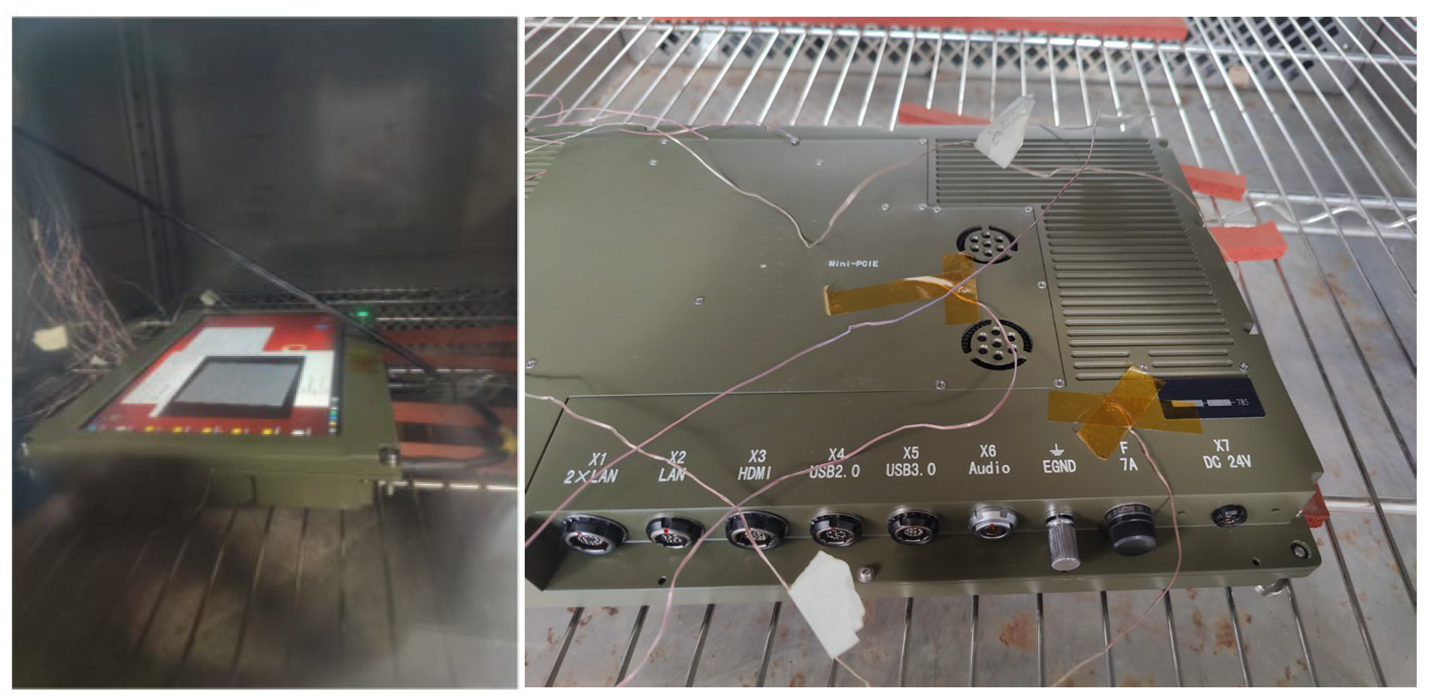
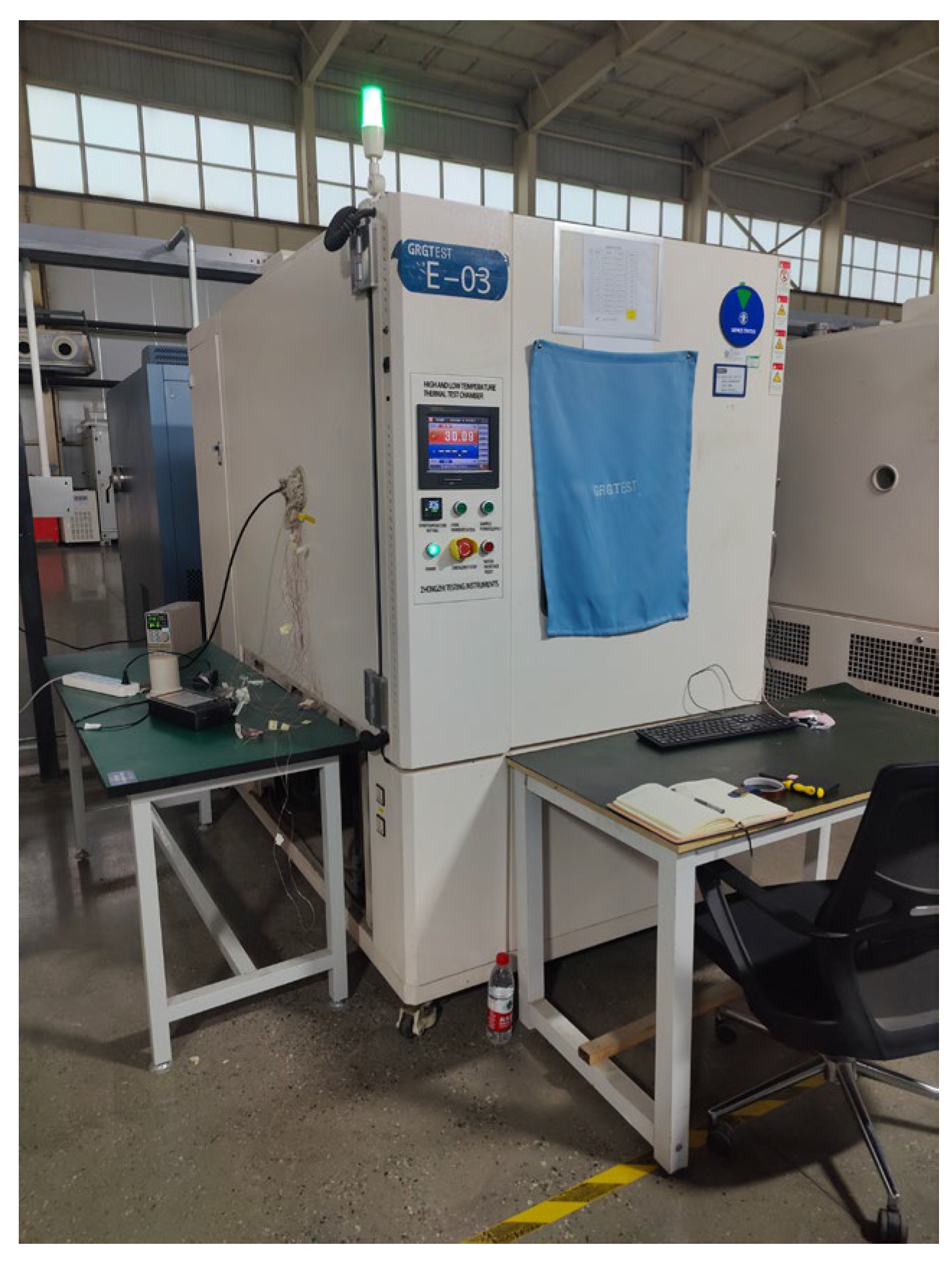
High-Low Temperature Test Chamber: The high-low temperature test chamber used is shown in Figure 14. This temperature-humidity test chamber has a temperature range of −100 °C to 500 °C, a humidity range of 10% to 98%, and a temperature change rate of up to 30 °C/min. Its performance indicators meet the requirements of China’s national standard GB0592-89 for high-low temperature test chambers, making it fully suitable for high-temperature testing of prototypes. It can meet the test requirements of a 25 °C to 55 °C temperature gradient for the fully enclosed ruggedized computer.
(4)
Data Processing Computer: It is connected to the Agilent 34970A Data Acquisition Unit via an RS232 interface, and the configuration of the data acquisition unit is performed using the Agilent Benchlink Data Logger Pro software (Version: 3.3.00).
(5)
Test Prototype: Manufactured based on the thermal optimization results.
(6)
Agilent Benchlink Data Logger Pro Data Acquisition Software: It can configure the data acquisition unit, including instrument status, channel parameters, thermocouple type, data collection, and data storage. It enables real-time data display and rapid analysis of measurement results.
The thermal testing system built for the fully enclosed ruggedized computer includes an experimental prototype, a temperature acquisition instrument, thermocouples, a high-low temperature test chamber, and a data processor. One end of the thermocouple is pasted on the position of the experimental prototype to be tested, and the other end is connected to the temperature acquisition instrument, which is connected to the data processor for real-time observation and processing of data. The high-low temperature test chamber provides different working environments for the experimental prototype, specifically an environmental gradient of 25 °C to 55 °C. The experimental prototype is placed in the high-low temperature test chamber. Before the experiment, a functional check of the prototype is required, then it is turned on, and a rendering program is called to ensure that the prototype runs at high power for the experiment. After the experiment at a certain temperature, the prototype is restored to room temperature, and then a functional check is performed again. The specific layout of the thermocouples is shown in Figure 15.

4.2. Thermal Test Process and Conclusions

4.2.1. Thermal Test Process

During the thermal test, Kepsen T-type adhesive thermocouples are mounted on the surface of the test objects. At the same time, all their built-in wires need to be led out and connected to the Agilent 34970A Data Acquisition Unit. Beforehand, labels indicating the name of each monitored object must be attached to the led-out wires, and the corresponding channels of the Agilent 34970A Data Acquisition Unit should be recorded.
The acquisition terminals of the Data Acquisition Unit are connected to the wire ends of all thermocouples. Install the Agilent Benchlink Data Logger software on the computer, then set the thermocouple type to T-type, the acquisition accuracy to 0.1, and match the acquisition channels with the names of the thermocouple wire ends. Set the acquisition interval to 5 s, and save the collected data in Excel format on the computer. By analyzing the collected data, the reliability and accuracy of the thermal optimization design and thermal simulation results are verified.
In the thermal testing process of this engineering prototype, it is mainly divided into the following steps:
  • Kepsen T-type adhesive thermocouples are arranged on the surface of the test objects to measure temperatures at 13 test points. These points include Chip 3A6000, Chip 7A2000, Chip X100, DDR4-1 memory, Chip 1860, Chip 2329, Chip a200, the heat pipes for Chip 3A6000, Chip 7A2000 and Chip X100, the condensation ends of the aforementioned heat pipes, and the fins on the chassis shell. After arranging the thermocouples, reassemble the engineering prototype.
  • Put the engineering prototype into the high-low temperature test chamber, power it on for initial inspection, record the inspection results, and after the inspection, turn off the prototype and cut off the power.
  • Raise the temperature of the high-low temperature test chamber to the specified temperature at a rate not exceeding 3 °C/min. The prototype is not powered on during the heating process. After reaching the specified temperature and balancing, maintain it for 2 h. Then, power on the prototype, start it up to perform rendering work, and use a data acquisition instrument to record the temperature values of the test objects. When the temperatures of all test objects stabilize, shut down the prototype and cut off the power.
  • Raise the temperature of the high-low temperature test chamber to the specified temperature at a rate not exceeding 3 °C/min. During the heating process, keep the prototype powered off. After reaching the specified temperature and achieving thermal equilibrium, maintain this temperature for 2 h. Then, power on the prototype and start it to perform rendering tasks, while using the Agilent 34970A Data Acquisition Unit to record the temperature values of the test objects. When the temperatures of all test objects stabilize, shut down the prototype and cut off its power supply.
Thermal tests and analyses were conducted under ambient temperatures with gradients of 25 °C, 40 °C, and 55 °C, respectively.
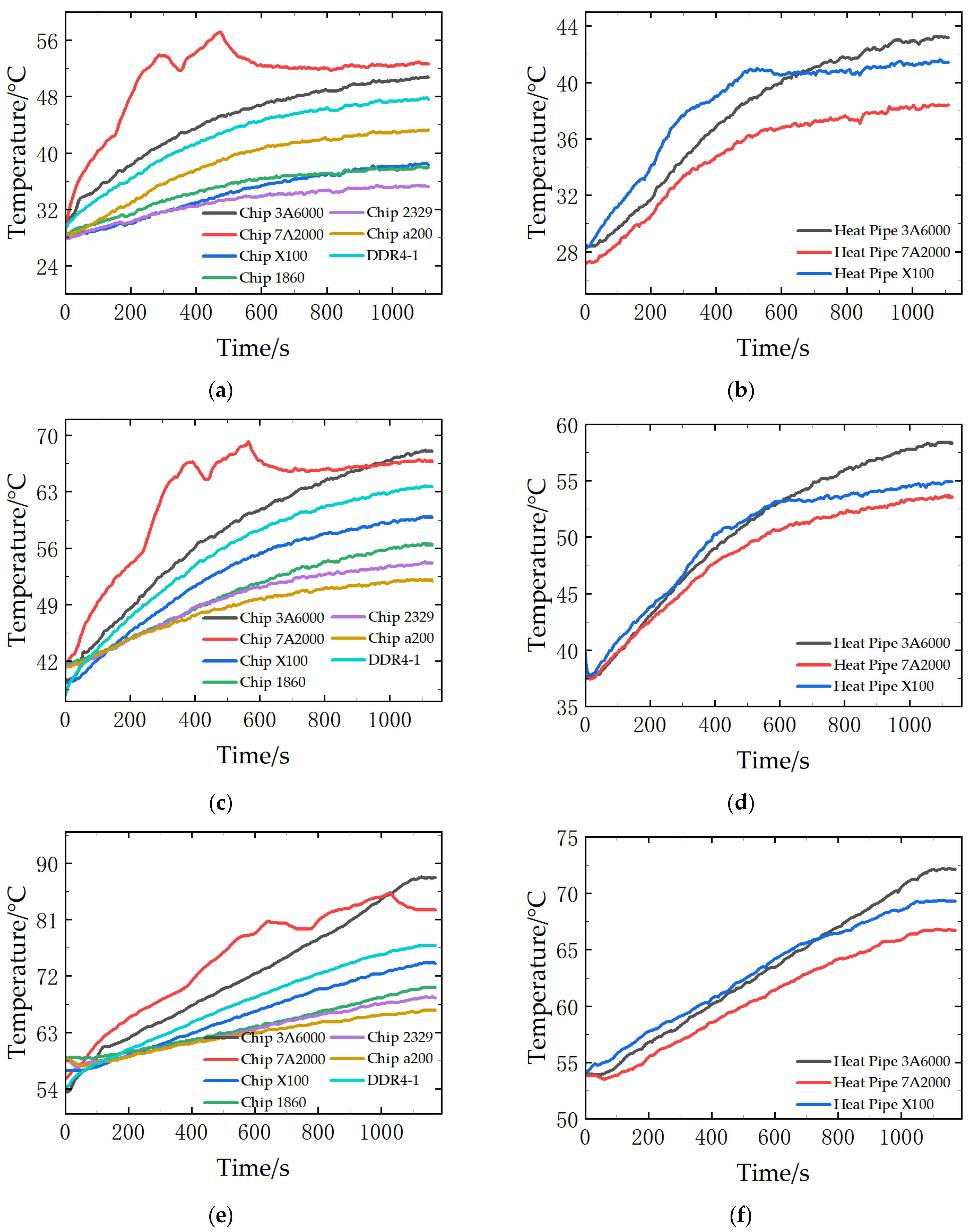
The experimental prototype was placed in a high-low temperature test chamber, and the temperature of the chamber was set to 25 °C, 40 °C, and 55 °C, respectively. After the temperature reached equilibrium, the prototype was powered on and put into rendering work. The working conditions of the prototype under the ambient temperatures of 25 °C, 40 °C, and 55 °C were observed, and the temperature data of the test objects were recorded. The specific test data are shown in Figure 16.

4.2.2. Quantification and Evaluation of Core Temperature Measurement Uncertainty

  • Type A Uncertainty: Evaluation of Random Effects
Type A uncertainty arises from random fluctuations in the measurement process (e.g., minor environmental disturbances, electronic noise of data loggers). It is calculated using statistical methods through multiple repeated measurements of the same measured object.
Taking the temperature measurement of Chip 3A6000 under a 55 °C environment as an example: the sampling period is 5 s, and 10 sets of data are recorded continuously after the temperature stabilizes. The data are shown in Table 13:
Calculation of the Arithmetic Mean:
T ¯ = 1 n i = 1 n T i = 86.580   ° C
In the formula, n represents the number of measurements, and T i denotes the temperature of each individual measurement. Calculation of Single-Measurement Standard Deviation:
s T i = 1 n 1 i = 1 n T i T ¯ 2 0.084   ° C
Finally, the standard uncertainty of the average value is obtained as follows:
u A T = s T i n 0.026   ° C
For other measured objects, such as Chip 7A2000 and heat pipe temperature difference, the Type A uncertainty is evaluated using the same method. Due to the consistent stability of the measurement system, the Type A uncertainty of all temperature measurements falls within the range of 0.02 °C to 0.03 °C, and u A = 0.03 °C is adopted in subsequent calculations.
2.
Type B Uncertainty: Evaluation of Systematic Effects
Type B uncertainty stems from the inherent errors of the measurement system (e.g., equipment accuracy limitations, process deviations). It is quantified based on equipment manuals, industry standards, and engineering experience, with the uncertainty calculation formula as follows:
u n T = Δ n C
where a is the allowable error corresponding to the measuring tool. For C: if following a uniform distribution, C is taken as 3 ; if following a normal distribution, C is taken as 2, with a confidence level of 95%.
According to the above formula, first, calculate the uncertainty caused by the thermocouple division error. In accordance with the IEC 60584-1 standard, the allowable error of a Class I Type T thermocouple within the range of −200 °C to 350 °C is ±0.5 °C. Following a uniform distribution, its uncertainty u 1 T = 0.290 °C.
Second, calculate the uncertainty caused by the measurement error of the data logger. The Agilent 34970A data logger has an allowable error of 0.01 °C, and the uncertainty obtained based on a normal distribution is u 2 = 0.005 °C.
Third, calculate the uncertainty caused by the temperature control error of the high-low temperature test chamber. Its control error is ±0.5 °C, and the uncertainty derived based on a uniform distribution is u 3 = 0.289 °C.
Finally, calculate the uncertainty caused by the contact thermal resistance error of the bonded thermocouple. The contact thermal resistance between the bonded thermocouple and the component surface leads to a deviation between the measured value and the actual surface temperature. According to engineering experience, the maximum value of this deviation is ±0.3 °C, and the uncertainty obtained based on a uniform distribution is u 4 = 0.173 °C.
All Type B uncertainty components are uncorrelated; therefore, the resulting combined Type B uncertainty is:
u B T = u 1 2 + u 2 2 + u 3 2 + u 4 2 0.44   ° C
Based on the Type A and Type B uncertainties, the combined standard uncertainty is obtained as follows:
u T = u A 2 + u B 2 0.44   ° C
Therefore, the raw data obtained from the experimental measurements are associated with the combined standard uncertainty. Taking the measured temperature of Chip 3A6000 as an example—under a 55 °C environment, the measured temperature is 86.6 °C—it is expressed as 86.60 °C ± 0.44 °C. This value is still lower than 90 °C, meeting the design requirements. After completing all data measurements, the conclusion is drawn as follows: Experiments have shown that when the fully enclosed ruggedized computer operates normally at ambient temperatures of 25 °C, 40 °C, and 55 °C, the temperatures of the three high-power chips, namely Chip 3A6000, Chip 7A2000, and Chip X100, are all within 90 °C; the temperatures of Memory DDR4-1, Chip 1860, Chip 2329, and Chip a200 are all within 75 °C; the temperature difference between the evaporation end and the condensation end of the three heat pipes is in the range of 5–20 °C, indicating that the heat pipes are in optimal performance; and the temperature of the fins on the chassis shell is within 80 °C. Therefore, the performance of the fully enclosed ruggedized computer with optimized thermal design has been greatly improved in the working environments of 25 °C, 40 °C, and 55 °C.

4.3. Comparison Between Experimental Data and Thermal Optimization Design Results

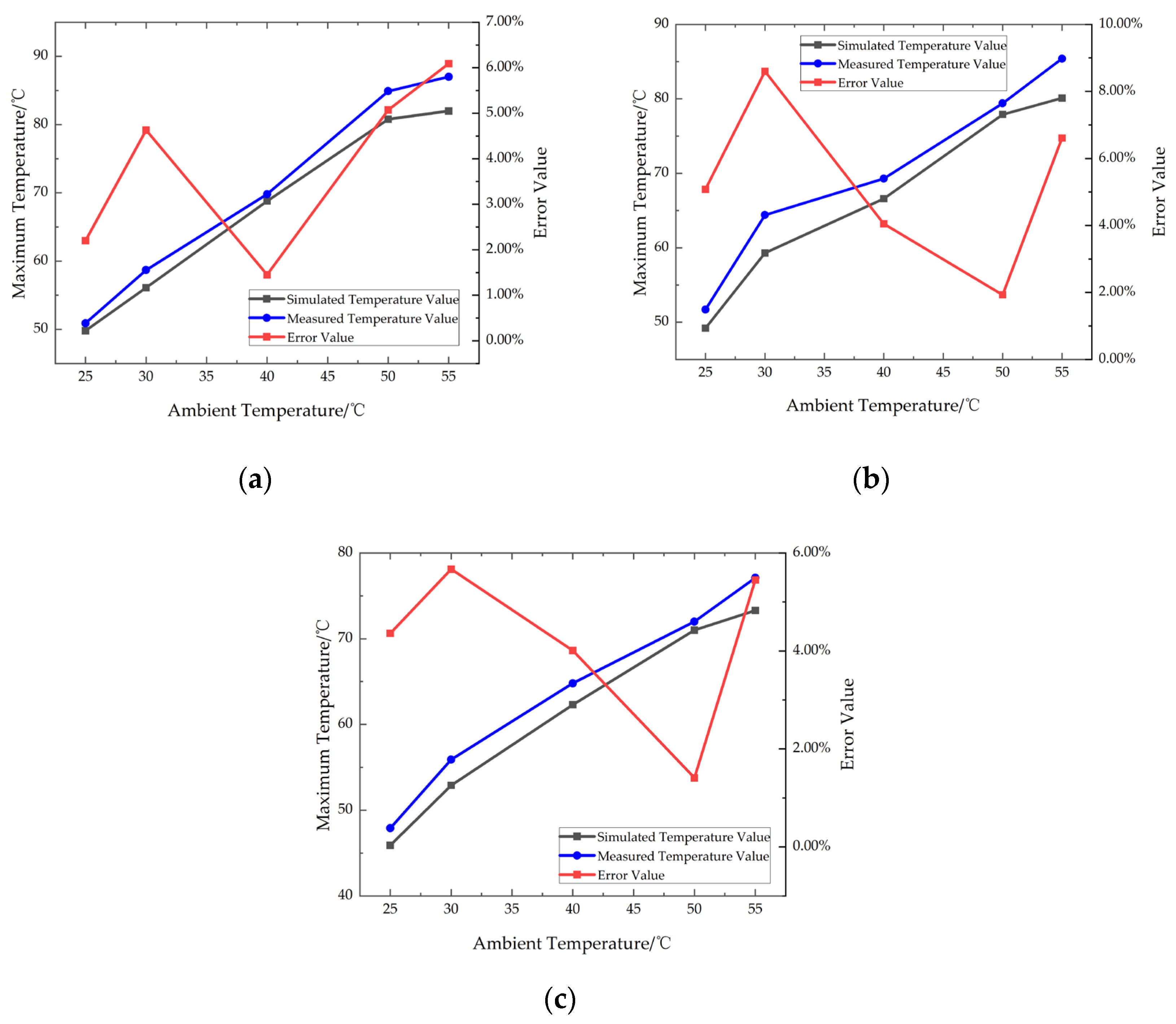
The optimal layout scheme of various components on the PCB board inside the chassis obtained through the P-MMAS algorithm, and the thermal simulation results under different ambient temperatures were obtained through re-modeling and thermal simulation analysis. The following figure shows the error comparison between the simulation data and experimental data of Chip 3A6000, Chip 7A2000 and Chip X100 under the working environment temperatures of 25 °C, 30 °C, 40 °C, 50 °C and 55 °C.
It can be seen from Figure 17a that the maximum error of Chip 3A6000 does not exceed 7%. As shown in Figure 17b, the maximum error of Chip 7A2000 is no more than 9%. From Figure 17c, it is observed that the maximum error of Chip X100 does not exceed 6%. Through the analysis of the errors between the simulation and experimental test values of the three main chips in the fully enclosed ruggedized computer, all error values are within 10%, which verifies the correctness of the simulation and the rationality of the thermal design.

5. Conclusions

This paper takes the fully enclosed ruggedized computer as the research object, conducts thermal layout optimization design for the components on the PCB board of the fully enclosed ruggedized computer to improve the heat dissipation performance of the computer, and performs thermal simulation analysis on the models of the fully enclosed ruggedized computer before and after optimization. Through testing the actual chassis model, the following conclusions are drawn:
(1)
The P-MMAS algorithm is proposed, and the optimal solution is selected based on the LINMAP decision-making method, followed by simulation verification. The simulation results indicate that for the model after layout optimization, when the ambient temperature is 55 °C, the temperature of Chip 3A6000 is 86.6 °C, Chip 7A2000 is 82.1 °C, Chip X100 is 74.8 °C, the maximum temperature of DDR4 memory is 78.8 °C, Chip 1860 is 74.1 °C, Chip 2329 is 73.4 °C, and Chip a200 is 72.1 °C. Compared with the pre-optimization state, the average temperature of the PCB decreases from 81.1 °C to 75.7 °C, verifying the effectiveness of the layout optimization. On the basis of the optimized PCB layout, thermal optimization design is conducted for the module layout inside the chassis. The results show that the fan module achieves the optimal performance when its coordinates are set to 20 mm (x-axis), 15 mm (y-axis), and 40 mm (z-axis). Re-modeling and simulation analysis results demonstrate that, compared with the initial empirical model at an ambient temperature of 55 °C: the maximum airflow velocity inside the chassis increases from 10.70 m/s to 13.08 m/s, indicating more intense air circulation; the temperature of Chip 3A6000 is 81.56 °C, Chip 7A2000 is 80.80 °C (corrected for possible typo), Chip X100 is 73.31 °C, the maximum temperature of DDR4 memory is 77.63 °C, Chip 1860 is 72.82 °C, Chip 2329 is 70.40 °C, and Chip a200 is 66.94 °C; the average temperature of the PCB is reduced to 73.12 °C. As can be seen from the optimization results, the thermal dissipation performance of the fully enclosed ruggedized computer can be improved through the layout optimization of components and in-chassis modules.
(2)
Thermal testing and verification of the temperature field under different ambient temperatures were conducted on the engineering prototype manufactured after the optimization of the fully enclosed ruggedized computer. The test results show that the equipment can meet the working requirements when the ambient temperature ranges from 25 °C to 55 °C. By comparing the experimental test data of the engineering prototype with the results of thermal simulation analysis, the errors are all within 10%, which verifies the correctness and rationality of the thermal simulation and thermal design.
This paper provides valuable guidance for thermal simulation, optimization design, etc., of fully enclosed ruggedized computers.

Author Contributions

Conceptualization, D.Z. and J.H.; methodology, R.F.; software, Fluent, R.F.; validation, D.Z.; investigation, D.C.; resources, D.Z., R.F. and P.L.; writing—original draft preparation, D.Z. and R.F.; writing—review and editing, P.L. and D.C.; supervision, J.H.; project administration, J.H. All authors have read and agreed to the published version of the manuscript.

Funding

This work was supported by the National Natural Science Foundation of China (No. U24B2053, 52035010).

Institutional Review Board Statement

Not applicable.

Informed Consent Statement

Not applicable.

Data Availability Statement

The raw data supporting the conclusions of this article will be made available by the authors on request.

Conflicts of Interest

The authors declare no conflicts of interest.

Abbreviations

The following abbreviations are used in this manuscript:
CPUCentral Processing Unit
GPUGraphics Processing Unit
FPGAField-Programmable Gate Array
P-MMASPareto-based Max-Min Ant System
LINMAPLinear Programming Techniques for Multidimensional Analysis of Preference
TDSThermal-Driven Swap
SGAStress Gradient Adjustment
DDR4Double Data Rate 4 Synchronous Dynamic Random Access Memory
PCBPrinted Circuit Board

References

  1. GJB 322A-1998; General Specification for Military Computers. General Armament Department of the PLA: Beijing, China, 1998.
  2. Li, S.; Guo, X. Design and simulation analysis of heat dissipation structure of motherboard of a certain type of portable rugged computer. J. Phys. Conf. Ser. 2024, 2761, 012011. [Google Scholar] [CrossRef]
  3. Wang, W.; Zheng, H.; Wang, J.; Ma, Y.; Li, S.; Liu, Y. Analysis of special-purpose computer on temperature field and optimization design. Chem. Eng. Trans. 2017, 61, 319–324. [Google Scholar]
  4. Yang, J.; Ye, N.; Shen, H.; Ye, D.; Zheng, W.; Di, J. A novel optimization algorithm for thermal design of MCMs. In Proceedings of the 2020 Chinese Control and Decision Conference (CCDC), Hefei, China, 22–24 August 2020; pp. 1567–1570. [Google Scholar]
  5. Vestias, M.; Neto, H. Trends of CPU, GPU and FPGA for high-performance computing. In Proceedings of the 2014 24th International Conference on Field Programmable Logic and Applications (FPL), Munich, Germany, 2–4 September 2014; pp. 1–6. [Google Scholar]
  6. Gizopoulos, D.; Papadimitriou, G.; Chatzidimitriou, A.; Reddi, V.J.; Salami, B.; Unsal, O.S.; Kestelman, A.C.; Leng, J. Modern hardware margins: Cpus, gpus, fpgas recent system-level studies. In Proceedings of the 2019 IEEE 25th International Symposium on On-Line Testing and Robust System Design (IOLTS), Rhodes, Greece, 1–3 July 2019; pp. 129–134. [Google Scholar]
  7. Yu, C.; Yu, X.; Yang, W. Preliminary research on thermal analysis/thermal design/thermal test technology for electronic equipment. Microelectronics 2000, 30, 334–337. [Google Scholar]
  8. Choi, U.-M.; Blaabjerg, F.; Jørgensen, S. Power cycling test methods for reliability assessment of power device modules in respect to temperature stress. IEEE Trans. Power Electron. 2017, 33, 2531–2551. [Google Scholar] [CrossRef]
  9. Andresen, M.; Ma, K.; Buticchi, G.; Falck, J.; Blaabjerg, F.; Liserre, M. Junction temperature control for more reliable power electronics. IEEE Trans. Power Electron. 2017, 33, 765–776. [Google Scholar] [CrossRef]
  10. Lakshminarayanan, V.; Sriraam, N. The effect of temperature on the reliability of electronic components. In Proceedings of the 2014 IEEE International Conference on Electronics, Computing and Communication Technologies (CONECCT), Bangalore, India, 6–7 January 2014; pp. 1–6. [Google Scholar]
  11. Campo, D.; Weyant, J.; Muzyka, B. Enhancing thermal performance in embedded computing for ruggedized military and avionics applications. In Proceedings of the Fourteenth Intersociety Conference on Thermal and Thermomechanical Phenomena in Electronic Systems (ITherm), Orlando, FL, USA, 27–30 May 2014; pp. 840–845. [Google Scholar]
  12. Luo, F.; Wang, Y.; Lui, Y.; Bai, J.; Yan, C.; Wei, Y.; Yuan, W.; Zhang, S.; Tang, Y. High-performance ultra-thin loop heat pipe enabled by screen–printing technology for enhancing heat dissipation of electronic devices. Appl. Therm. Eng. 2025, 279, 127479. [Google Scholar] [CrossRef]
  13. Jang, H.-Y. Innovative optimal control methodology of heat dissipation in electronic devices. J. Thermophys. Heat Transf. 2008, 22, 563–571. [Google Scholar] [CrossRef]
  14. Tang, L.; Joshi, Y.K. Integrated thermal analysis of indirect air-cooled electronic chassis. IEEE Trans. Compon. Packag. Manuf. Technol. Part A 1997, 20, 103–110. [Google Scholar] [CrossRef]
  15. Huang, J.F. Structure design of a fully enclosed airborne reinforcement computer. In Proceedings of the CCF National Conference on Computer Engineering and Technology, Enshi, China, 1–2 August 2019; pp. 101–111. [Google Scholar]
  16. Saste, S.; Doshi, H.; Khalate, P.; Jedhe, S.; Yadav, N. Modification in Heat Sink Design to Improve its Heat Dissipation Capacity for Current CPU Design. STM J. J. Energy Environ. Carbon Credit. 2018, 8, 1–7. [Google Scholar]
  17. Hussain, I.Y.; Abdulla, H.S. Optimization of Thermal Layout Design of Electronic Equipments on the Printed Circuit Board. J. Eng. 2006, 12, 757–775. [Google Scholar] [CrossRef]
  18. Huang, Y.-J.; Fu, S.-L. Thermal placement design for MCM applications. J. Electron. Packag. 2000, 122, 115–120. [Google Scholar] [CrossRef]
  19. Wang, L.; Lu, G.; Yang, K. Thermal optimization of electronic devices on PCB based on the ant colony algorithm. In Proceedings of the 2018 International Conference on Electronics Technology (ICET), Chengdu, China, 23–27 May 2018; pp. 55–59. [Google Scholar]
  20. Pang, Y.F.; Scott, E.P.; Chen, J.Z.; Thole, K.A. Thermal design and optimization methodology for integrated power electronics modules. J. Electron. Packag. 2005, 127, 59–66. [Google Scholar] [CrossRef]
  21. Huang, X.; Hu, J.; Ge, Y.; Guo, L.; Han, K.; Zhang, J. Automatic optimization system for heat source layout of multi-chip components based on multi-software integration. Appl. Sci. 2024, 14, 4577. [Google Scholar] [CrossRef]
  22. Luo, D.; Zhao, Y.; Wang, Z.; Li, G. Thermal Layout Optimization of Power Devices on PCB. In Proceedings of the International Conference on Wireless Power Transfer, Weihai, China, 13–15 October 2023; pp. 181–188. [Google Scholar]
  23. Su, C.-J.; Zhao, T. Collaborative optimization of thermal conductivity distribution and heat source layout based on Bayesian optimization. Int. J. Heat Mass Transf. 2024, 224, 125324. [Google Scholar] [CrossRef]
  24. Zhao, J.; Wang, H.; Yao, W.; Peng, W.; Gong, Z. An online surrogate-assisted neighborhood search algorithm based on deep neural network for thermal layout optimization. Complex Intell. Syst. 2024, 10, 2459–2475. [Google Scholar] [CrossRef]
  25. Ismail, F.S.; Yusof, R. Thermal optimization formulation strategies for multi-constraints electronic devices placement on PCB. In Proceedings of the TENCON 2009—2009 IEEE Region 10 Conference, Singapore, 23–26 November 2009; pp. 1–6. [Google Scholar]
  26. Zhang, Z.; Abas, A.; Dan, J.; Ani, F.C. Numerical Analysis of Thermal Performance in Semi-Enclosed Electronics: Investigating Active and Passive Cooling Techniques for SSD-Driven Single-Board Devices. Results Eng. 2025, 27, 106669. [Google Scholar] [CrossRef]
  27. Jeevan, K.; Quadir, G.; Seetharamu, K.; Azid, I. Thermal management of multi-chip module and printed circuit board using FEM and genetic algorithms. Microelectron. Int. 2005, 22, 3–15. [Google Scholar] [CrossRef]
  28. Suwa, T.; Hadim, H. Multidisciplinary placement optimization of heat generating electronic components on a printed circuit board in an enclosure. IEEE Trans. Compon. Packag. Technol. 2007, 30, 402–410. [Google Scholar] [CrossRef]
  29. Cheng, H.-C.; Chung, I.-C.; Chen, W.-H. Thermal chip placement in MCMs using a novel hybrid optimization algorithm. IEEE Trans. Compon. Packag. Manuf. Technol. 2012, 2, 764–774. [Google Scholar] [CrossRef]
  30. Zhao, J. Finite Element Model and Simulation for Thermal-Mechanical Analysis of PCB Assemblies; Tianjin University: Tianjin, China, 2006. [Google Scholar]
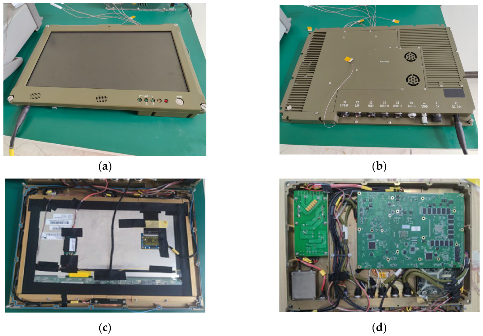
Figure 1. Display Diagram of the Fully Enclosed Ruggedized Computer. (a) Diagram of the front display of the complete machine; (b) Diagram of the rear shell of the complete machine; (c) Diagram of the internal display; (d) Diagram of Internal Component Layout.
Machines 13 01067 g001
Figure 2. Chassis Model. (a) Actual Chassis Enclosure; (b) Actual Chassis Internal Structure; (c) Simulated Chassis Enclosure; (d) Simulated Chassis Internal Structure.
Machines 13 01067 g002
Figure 3. Air domain inside the chassis.
Machines 13 01067 g003
Figure 4. Mesh generation.
Machines 13 01067 g004
Figure 5. Simulation of the Initial Model at Different Temperatures. (a) Simulation of PCB and Components at an Ambient Temperature of 40 °C; (b) Simulation of PCB and Components at an Ambient Temperature of 55 °C; (c) Temperature Distribution of Heat Pipes at an Ambient Temperature of 40 °C; (d) Temperature Distribution of Heat Pipes at an Ambient Temperature of 55 °C.
Machines 13 01067 g005
Figure 6. Mesh division and component position numbering diagram.
Machines 13 01067 g006
Figure 7. Three-dimensional Pareto frontier.
Machines 13 01067 g007
Figure 8. Two-dimensional Pareto frontier distribution and representation of solutions. (a) Pareto frontier graph of the maximum temperature and maximum deformation displacement of the PCB board; (b) Pareto frontier graph of the maximum temperature difference between PCB boards and maximum deformation displacement; (c) Pareto frontier graph of the maximum temperature of the PCB board and the maximum temperature difference between PCB boards.
Machines 13 01067 g008
Figure 9. Two-dimensional plan view of component layout positions before and after optimization. (a) Initial layout; (b) Optimized layout.
Machines 13 01067 g009
Figure 10. Simulation results. (a) Chassis temperature; (b) PCB temperature; (c) PCB deformation under random vibration; (d) PCB deformation under transient impact.
Machines 13 01067 g010
Figure 11. Maximum temperature of each module after optimization varies with the working environment temperature. (a) Maximum temperature of each device; (b) Maximum temperature of each heat pipe; (c) Maximum temperature of each fin; (d) Temperature of each module of the chassis.
Machines 13 01067 g011
Figure 12. Comparison of maximum steady-state temperatures of various components under different ambient temperatures before and after optimization. (a) Chip 3A6000; (b) Chip 7A2000; (c) Chip X100; (d) Chip 1860; (e) Chip 2329; (f) Chip a200; (g) Uniform temperature of PCB board; (h) Uniform temperature of chassis shell.
Machines 13 01067 g012aMachines 13 01067 g012b
Figure 13. Simulation Results of the Finally Optimized Chassis. (a) Temperature Distribution of the Chassis Shell; (b) Temperature Distribution of the PCB and Components; (c) Velocity Vector Diagram of a Cross-Section Inside the Initial Chassis; (d) Velocity Vector Diagram of a Cross-Section Inside the Finally Optimized Chassis.
Machines 13 01067 g013
Figure 14. High-Low temperature test chamber.
Machines 13 01067 g014
Figure 15. Thermocouple layout of the thermal test system. (a) Front layout; (b) Chassis layout.
Machines 13 01067 g015
Figure 16. Temperature changes in each test object. (a) Component temperatures at 25 °C; (b) Temperatures of each heat pipe at 25 °C; (c) Component temperatures at 40 °C; (d) Temperatures of each heat pipe at 40 °C; (e) Component temperatures at 55 °C; (f) Temperatures of each heat pipe at 55 °C.
Machines 13 01067 g016
Figure 17. Comparison of errors of various devices under working environments of 25~55 °C. (a) Chip 3A6000; (b) Chip 7A2000; (c) Chip X100.
Machines 13 01067 g017
Table 1. Material property settings.
Component Density   ( k g / m 3 ) Specific   Heat   Capacity   ( J / k g K ) Thermal Conductivity
( W / m K )
Chassis Shell 2719871202.4
Display25008501.4
PCB1900115035.0
Heat-generating Components2300712148.0
Heat Pipe8978381387.6
Deionized Water99741860.6
Thermal Pad310075015.0
Table 2. Specific parameters of components and devices.
NameQuantityPower ( W )Length × Width × Height
( m m )
Allowable Temperature
( ° C )
Chip 3A6000 138.035 × 35 × 2.5−40~90
Chip 7A2000135.029 × 29 × 2.0−40~85
Chip X100115.031 × 31 × 1.8−40~85
DDR4 memory chip163.08 × 6 × 1.285
Chip A20010.56 × 4 × 1.0−55~150
Chip 232910.35 × 3 × 1.0−40~105
Chip 186020.87 × 5 × 1.2−40~85
Table 3. Basic parameters of the equipment.
NameActual ModelNameEquivalent Model 2
Chassis dimensions518 mm × 338 mm × 53.37 mmOperating temperature−40 °C~55 °C
Chassis mass8.22 kgOperating voltageDC: 24 V
Total power consumption of the device109.9 WProtection classIP67
Table 4. Component position coding.
Component Reference DesignatorPosition CoordinatesComponent Reference DesignatorPosition Coordinates
Q1(23, 13)D8(42, 13)
Q2(18, 13)D9(42, 15)
Q3(9, 13)D10(42, 17)
Q4(11, 22)D11(42, 19)
D1(30, 8)D12(42, 23)
D2(32, 8)D13(40, 23)
D3(34, 8)D14(38, 23)
D4(36, 8)D15(36, 23)
D5(38, 8)D16(34, 23)
D6(40, 8)U1(36, 16)
D7(42, 11)U2(20, 19)
Table 5. Results obtained without introducing the Pareto solution set.
Solution NumberMaximum PCB Temperature
T max (°C)
Maximum PCB Temperature Difference Δ T (°C)Maximum PCB Deformation
d max (mm)
184.220.50.032
289.513.00.027
388.114.90.024
486.614.50.028
586.417.10.031
Table 6. Component position coding after layout optimization.
Component Reference DesignatorPosition CoordinatesComponent Reference DesignatorPosition Coordinates
Q1(8, 28)D8(33, 28)
Q2(8, 10)D9(25, 5)
Q3(4, 10)D10(26, 11)
Q4(8, 14)D11(33, 2)
D1(29, 25)D12(26, 26)
D2(25, 24)D13(30, 27)
D3(39, 6)D14(40, 11)
D4(34, 6)D15(40, 27)
D5(25, 7)D16(37, 26)
D6(40, 25)U1(34, 15)
D7(29, 4)U2(4, 21)
Table 7. Comparison between the optimal decision solution and the results of the actual simulation model.
PCB Board DataActual modelLINMAPRelative Error
Maximum temperature86.579 °C85.34 °C1.4%
Temperature difference21.658 °C22.42 °C3.5%
Maximum deformation0.028 mm0.02875 mm2.6%
Table 8. Comparison of thermal simulation results before and after optimization of component layout on the PCB board inside the chassis.
DeviceTemperature Before Optimization (°C)Temperature
After Optimization (°C)
DeviceTemperature Before Optimization (°C)Temperature
After Optimization (°C)
Chip 3A600091.186.6DDR4-1089.179.2
Chip 7A200086.982.1DDR4-1188.680.7
Chip X10079.174.8DDR4-1287.074.6
DDR4-185.772.5DDR4-1387.476.5
DDR4-286.775.7DDR4-1487.781.3
DDR4-387.380.5DDR4-1587.579.0
DDR4-487.781.2DDR4-1686.979.6
DDR4-587.678.0Chip 186074.274.1
DDR4-687.379.2Chip232984.173.4
DDR4-788.280.3Chip a20080.372.1
DDR4-888.977.9PCB Board80.175.7
DDR4-989.279.4Chassis Shell73.068.8
Table 9. Factor-Level Table.
Test NumberRadius of the Fan r (mm)X-Coordinate (mm)Y-Coordinate (mm)Z-Coordinate (mm)
1201011230
2162012220
312301330
48401440
55501550
Table 10. Experimental Scheme and Results at a Working Ambient Temperature of 55 °C.
Test NumberRadius of the Fan r (mm)X-Coordinate x (mm)Y-Coordinate y (mm)Z-Coordinate z (mm)Maximum Temperature
(°C)
Chip
3A6000
Chip
7A2000
Chip
X100
PCB Average Temperature
1111181.8079.0774.6374.77
2123480.7878.0774.1773.46
3135279.8678.5974.2974.09
4142580.7878.2674.2573.88
5154382.7178.5773.9573.92
6215483.1378.9874.2574.46
7222283.3979.3774.7374.95
8234583.0078.5474.1474.10
9241383.0579.0474.3574.52
10253183.2479.2874.6374.82
11314282.2678.6174.0874.28
12321583.1878.8774.4174.48
13333382.9078.9474.2674.50
14345183.1479.1974.5274.75
15352483.0578.8874.3274.47
16413582.7078.6174.0874.09
17425383.1178.7774.4274.27
18432182.6079.0174.4774.66
19444482.0178.1574.0673.73
20451280.8979.0774.7874.72
21512381.7878.1874.0573.63
22524182.7978.9974.4574.58
23531481.6478.2174.0273.93
24543283.1079.1374.5274.60
25555582.2978.3874.2973.90
Table 11. Range Analysis Table.
ItemLevel r x y z
K Value1370.550372.230372.340373.340
2373.010371.440371.750372.440
3373.120371.810371.640371.700
4371.830371.640371.960370.670
5370.730372.120371.550371.090
Kavg Value174.11074.44674.46874.668
274.60274.28874.35074.488
374.62474.36274.32874.340
474.36674.32874.39274.134
574.14674.42474.3174.218
Optimal Level1254
R0.5140.1580.1580.534
Table 12. Comparison of thermal simulation results before and after optimization of module layout in the chassis.
DeviceTemperature Before Optimization (°C)Temperature After Optimization (°C)DeviceTemperature Before Optimization (°C)Temperature
After Optimization (°C)
Chip 3A600091.181.6DDR4-1089.176.8
Chip 7A200086.980.8DDR4-1188.678.5
Chip X10079.173.3DDR4-1287.072.6
DDR4-185.771.9DDR4-1387.474.9
DDR4-286.774.3DDR4-1487.779.9
DDR4-387.379.8DDR4-1587.578.1
DDR4-487.779.8DDR4-1686.977.3
DDR4-587.676.7Chip 186074.273.3
DDR4-687.375.4Chip 232984.170.4
DDR4-788.279.2Chip a20080.366.9
DDR4-888.975.7PCB Board80.173.1
DDR4-989.277.6Chassis Shell73.067.9
Table 13. Measured Data of Chip 3A6000.
Number of Measurements12345678910
Temperature
(°C)
86.586.686.586.786.686.586.686.786.586.6
Disclaimer/Publisher’s Note: The statements, opinions and data contained in all publications are solely those of the individual author(s) and contributor(s) and not of MDPI and/or the editor(s). MDPI and/or the editor(s) disclaim responsibility for any injury to people or property resulting from any ideas, methods, instructions or products referred to in the content.