1. Introduction
The explosive growth of digital multimedia and communication networks has led to unprecedented demand for secure, high-speed data transmission. Applications such as high-definition streaming, real-time communication, and IoT sensing generate large volumes of encrypted data. In these scenarios, any encryption-related bottleneck can severely degrade system performance or user experience. To meet this demand, hardware-based cryptographic modules have become indispensable, offering orders-of-magnitude improvements in throughput and energy efficiency over software-only solutions. Hardware accelerators perform encryption and decryption without creating bottlenecks in data pipelines, making them especially attractive for high-bandwidth networks and resource-constrained IoT devices [
1,
2].
Among symmetric-key encryption algorithms, the Advanced Encryption Standard (AES) has emerged as the de facto cipher for securing digital information [
3]. In particular, the 128-bit variant (AES-128) is widely used in practice due to its strong security properties and relatively efficient design [
4] standardised by the National Institute of Standards and Technology (NIST). AES-128 processes 128-bit data blocks through ten rounds of substitution and permutation operations. Its well-defined transformations—byte-wise Sub Bytes, row shifts (Shift Rows), and column mixing (Mix Columns)—are particularly amenable to parallel and pipelined hardware implementation. Consequently, AES-128 is embedded in numerous communication and security standards (e.g., TLS/SSL, IPsec, and wireless protocols), underlining the importance of high-performance AES cores.
However, combining low latency with high throughput in an ASIC implementation of AES-128 remains challenging. A straightforward AES round combines several nonlinear and linear transformations in sequence, resulting in a long critical path that limits the maximum clock frequency. Techniques such as loop unrolling and deep pipelining can significantly increase throughput by breaking the computation into parallel stages, but these approaches often incur considerable area and power overhead due to additional registers and duplicated logic. Conversely, compact designs that minimise hardware resources generally cannot achieve comparable clock speeds. As a result, AES-128 hardware designers face an inherent trade-off between performance (latency and throughput) and implementation cost (area and power).
Unlike conventional AES hardware implementations that rely primarily on coarse inter-round pipelining or full loop unrolling, the proposed architecture introduces a balanced intra-round and inter-round pipelining strategy placement specifically targeting the MixColumns critical path, which is the dominant contributor to delay. In this approach, pipeline registers are carefully inserted not only between AES rounds but also within critical transformation blocks, particularly around the MixColumns operation, which dominates the critical path.
This fine-grained pipeline placement significantly reduces the combinational delay without introducing redundant logic or excessive register overhead.
Furthermore, the design ensures proper synchronisation between the datapath and key expansion pipeline, thereby avoiding round-key misalignment issues commonly observed in deeply pipelined AES architectures. This balanced strategy enables high opera ting frequency while maintaining efficient area and power utilisation.
Post-synthesis results indicate that the proposed AES-128 core operates at a clock frequency of 1.39 GHz in a 65 nm standard-cell CMOS technology, demonstrating suitability for high-speed secure communication systems [
5,
6]. The architecture is fully pipelined, with registers strategically placed between the Sub Bytes, Mix Columns, and Add Round Key transformations to reduce the critical path delay [
5]. This design achieves a per-round encryption latency on the order of a few hundred picoseconds in a 65 nm process. A Universal Verification Methodology (UVM) testbench is developed to provide comprehensive functional verification and coverage analysis. The design is synthesised using the Cadence Genus tool (2019.2) suite to obtain realistic timing, area, and power estimates. Experimental results demonstrate that the AES-128 core can operate at approximately 1.3 GHz while maintaining a compact area footprint, highlighting its suitability for secure, high-speed communication and resource-constrained embedded systems [
6].
In summary, the main contributions of this work are:
A more focused pipeline placement methodology is proposed, co-locating intra-round and inter-round pipelining with particular optimisation of the MixColumns transformation, which is recognised as the largest portion of the critical path in AES datapaths.
The design avoids synchronisation problems between the datapath and key expansion module, thereby avoiding round-key misalignment in heavily pipelined designs.
A fully modular SystemVerilog RTL design of a 128-bit AES encryption core is created for scalable ASIC design and hardware reuse.
A UVM-based verification environment is developed to verify the correctness of the pipeline, key expansion and data processing for each round.
An ASIC-oriented design flow with Cadence Genus synthesis tool is adopted to achieve realistic post-synthesis timing, area and power metrics with a maximum clock speed of 1.39 GHz and a lower critical path delay of around 300 ps.
Performance analysis with existing FPGA- and ASIC-based AES designs presents better timing efficiency and applicability for high-speed secure communication applications.
All frequency values are expressed in hertz-based SI units, and all delay values are expressed in seconds.
The rest of this paper is structured as follows. In
Section 3, we describe the design and implementation of the proposed AES-128 architecture, its pipelining approach and verification plan.
Section 4 reports the post-synthesis evaluation outcomes in terms of timing, area and power, and compares them with previous work. Finally,
Section 5 concludes the paper and provides suggestions for future work.
2. Literature Review
Recent AES hardware research can be broadly classified into three categories:
- (i)
high-throughput FPGA implementations,
- (ii)
compact low-power ASIC cores, and
- (iii)
reliability-oriented secure architectures.
However, only a limited number of studies address balanced pipelining strategies targeting critical path reduction in ASIC flows.
Other studies have prioritised minimising area and power for resource-constrained applications [
7,
8]. Iterative AES architectures and reduced-width Datapath (for instance, 8-bit or byte-serial designs) have been proposed to lower logic usage and energy consumption. These compact implementations, while saving silicon area, typically achieve only moderate throughput and often omit a complete functional verification stage [
9]. In parallel, reliability and testability enhancements have been explored: for example, hybrid pipelining with built-in error detection and on-chip BIST mechanisms have been integrated to improve robustness [
10]. Such designs focus on fault tolerance but frequently introduce overhead and still do not provide a unified ASIC synthesis or PPA evaluation.
More recent efforts emphasise ASIC-oriented evaluation [
8]. A few works have employed complete ASIC design flows (e.g., synthesising with Cadence Genus) and adopted industry-standard verification methodologies like the Universal Verification Methodology (UVM). Nevertheless, most AES hardware publications continue to focus on either FPGA prototyping or isolated aspects of design. For instance, an ASIC BIST-enabled AES processor might report some timing metrics but omit power and area figures, whereas a high-speed FPGA implementation might attain impressive clock rates but lack any ASIC post-synthesis data. In general, very few existing works combine a full RTL description of AES-128, UVM-based validation, and post-synthesis ASIC PPA evaluation in a single study.
Although prior works report high throughput or compact area, most designs either rely on FPGA-centric evaluation or do not present detailed post-synthesis timing closure with balanced pipeline placement. Therefore, a gap exists in ASIC-oriented AES architectures that simultaneously address timing, verification, and scalable RTL modularity.
While the AES encryption technique was the focus of most contemporary papers, other approaches have also been examined in the literature, including multimedia and chaos-based encryption methods, which aim at providing security for image and video data. The encryption method is known to have high sensitivity and key space; however, it has a high computational overhead and can thus not be implemented in hardware efficiently. As a result, deterministic schemes like the AES are preferred and efficient for ASIC-based applications. Apart from AES encryption algorithms, contemporary research has also paid attention to advanced encryption algorithms such as image encryption algorithms and chaos-based encryption algorithms. For instance, the Re-cropping Framework: A Grid Recovery Method for Quantisation Step Estimation in Non-aligned Recompressed Images [
11] provides an effective approach for image integrity analysis and quantisation estimation. Similarly, the multi-layer and multi-directional image encryption algorithm based on the hyperchaotic 3D Xin-She Yang map [
12] introduces a robust encryption mechanism using chaotic systems and multi-dimensional transformations. The EAS framework employs neuron-inspired chaotic dynamics for multimedia video encryption, improving randomness and key sensitivity, but without ASIC-oriented timing or hardware implementation analysis. In terms of performance evaluation, chaos-based and multimedia encryption techniques generally provide high security due to complex nonlinear dynamics and large key spaces. However, these methods involve significantly higher computational complexity and are not well-suited for efficient hardware implementation. In contrast, AES-based architectures rely on well-defined substitution–permutation operations that are highly optimised for digital hardware. As a result, AES offers a balanced trade-off between security, computational efficiency, and hardware feasibility, making it more suitable for ASIC-based high-throughput applications. The work proposed here is to optimise the AES for high-frequency ASIC implementation, with priority to timing performance and efficiency.
Table 1 summarises representative AES-128 hardware implementations from the recent literature, indicating their platform, focus, key techniques, and limitations. It highlights that while many designs excel in a particular metric (such as throughput or area efficiency), they often lack comprehensive ASIC evaluation or exhaustive verification. To the best of our knowledge, no prior work presents a complete end-to-end ASIC-ready AES-128 implementation with detailed RTL design, rigorous UVM verification, and full post-synthesis PPA analysis. This gap motivates the need for an integrated ASIC-oriented design flow, which the present study addresses.
As shown in
Table 2, for a broader comparison with modern multimedia and chaos-based encryption frameworks, the proposed AES-128 architecture is evaluated on several aspects, including the structure of the encryption, computational complexity, feasibility of hardware implementation, optimisation of computation time, and the possibility of implementing the architecture in an application-specific integrated circuit (ASIC).
The comparison indicates that multimedia-oriented chaotic encryption methods prioritise statistical security metrics, whereas the proposed AES-128 architecture focuses on deterministic hardware optimisation, timing closure, and synthesisable high-throughput ASIC implementation.
The EAS, 3D-NDHC, and MLMD-IE are recent chaos-based and multimedia encryption schemes, which mainly enhance security in statistical aspects through hyperchaotic diffusion, multidimensional permutation, and nonlinear sequence generation. The MLMD-IE and Re-cropping frameworks mainly focus on multidimensional diffusion security and forensic image analysis, respectively, but do not address high-frequency pipelined ASIC-oriented cryptographic hardware implementation. Usually, these techniques are assessed from entropy, NPCR, UACI, correlation and Lyapunov exponent analysis. Most of these schemes, however, are software-based and fail to measure ASIC-oriented parameters like timing closure, post-synthesis delay, pipeline feasibility or hardware resource usage. Conversely, the proposed AES-128 architecture is optimally designed to be implemented in an ASIC with deterministic substitution–permutation operations and balanced pipelining for high throughput. The proposed work also involves verification using UVM and post-synthesis evaluation using Cadence Genus, which allows for the direct analysis of timing performance and hardware feasibility.
3. AES-128 Architecture and Implementation
3.1. Overview of AES Cryptographic Algorithm
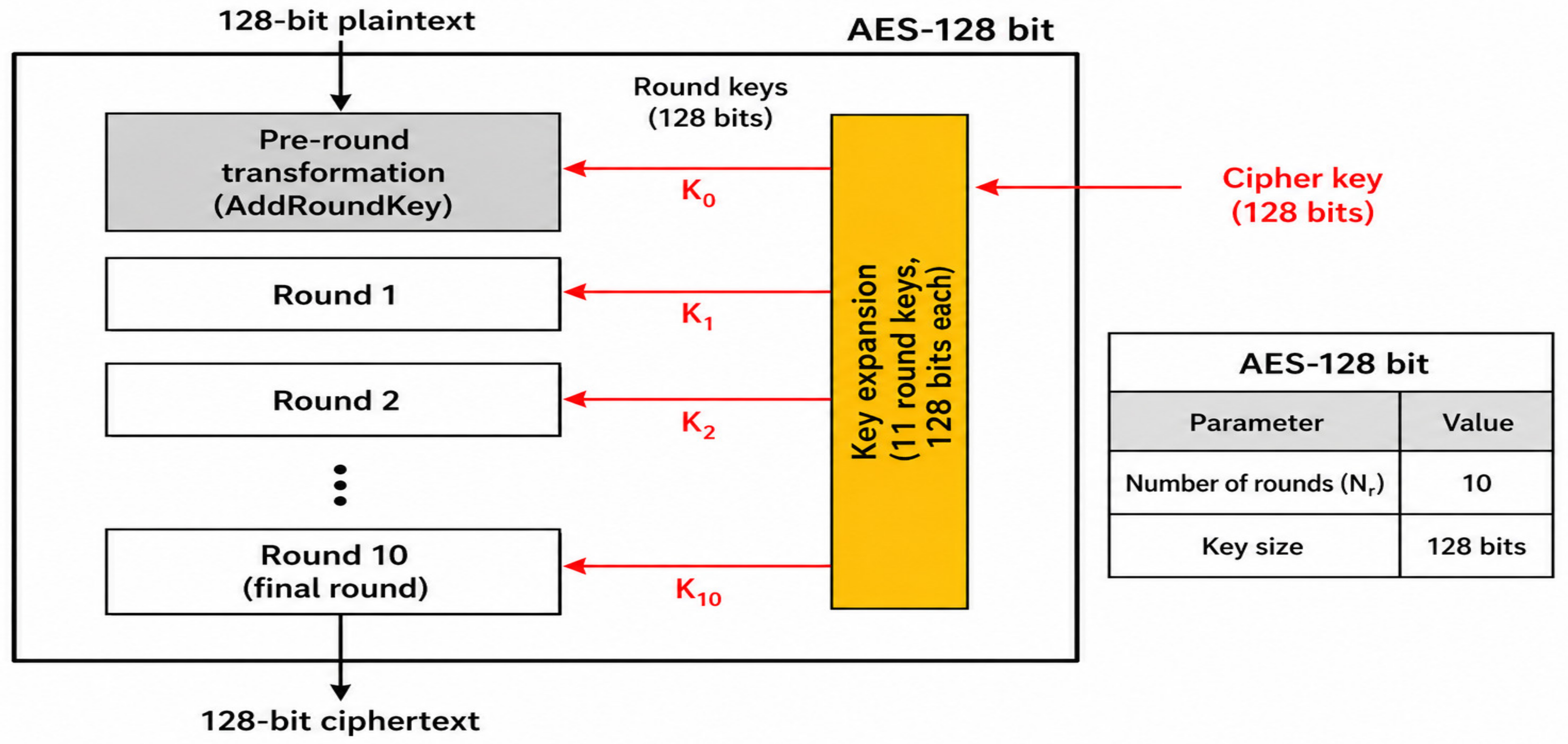
AES-128 is a symmetric-key block cipher operating on 128-bit data blocks and 128-bit keys [
10]. It follows a fixed 4 × 4 byte-state substitution–permutation network (SPN).
The AES state is represented as a 4 × 4 matrix of bytes (16 bytes total), arranged in four columns and four rows. Under the FIPS-197 standard, a 128-bit key requires 10 rounds [
10]. Prior to encryption, a key schedule expands the cipher key into 11 separate 128-bit round keys (one for the initial round and one for each of the 10 rounds). Each round applies a sequence of byte-wise and word-wise operations to introduce confusion and diffusion in the state. In particular, every round (except the last) consists of four transformations executed in order [
13].
Figure 1 illustrates the overall AES-128 encryption process along with the 4 × 4 state matrix representation.
SubBytes: SubBytes performs nonlinear byte substitution using a fixed GF(2
8)-based S-box to introduce confusion in the AES state. The AES standard defines this S-box as having no fixed points and providing strong nonlinearity [
13].
ShiftRows: A byte-wise permutation that cyclically rotates the last three rows of the 4 × 4 state by offsets of 1, 2, and 3 bytes (the first row is unchanged). This step spreads byte differences across columns [
13].
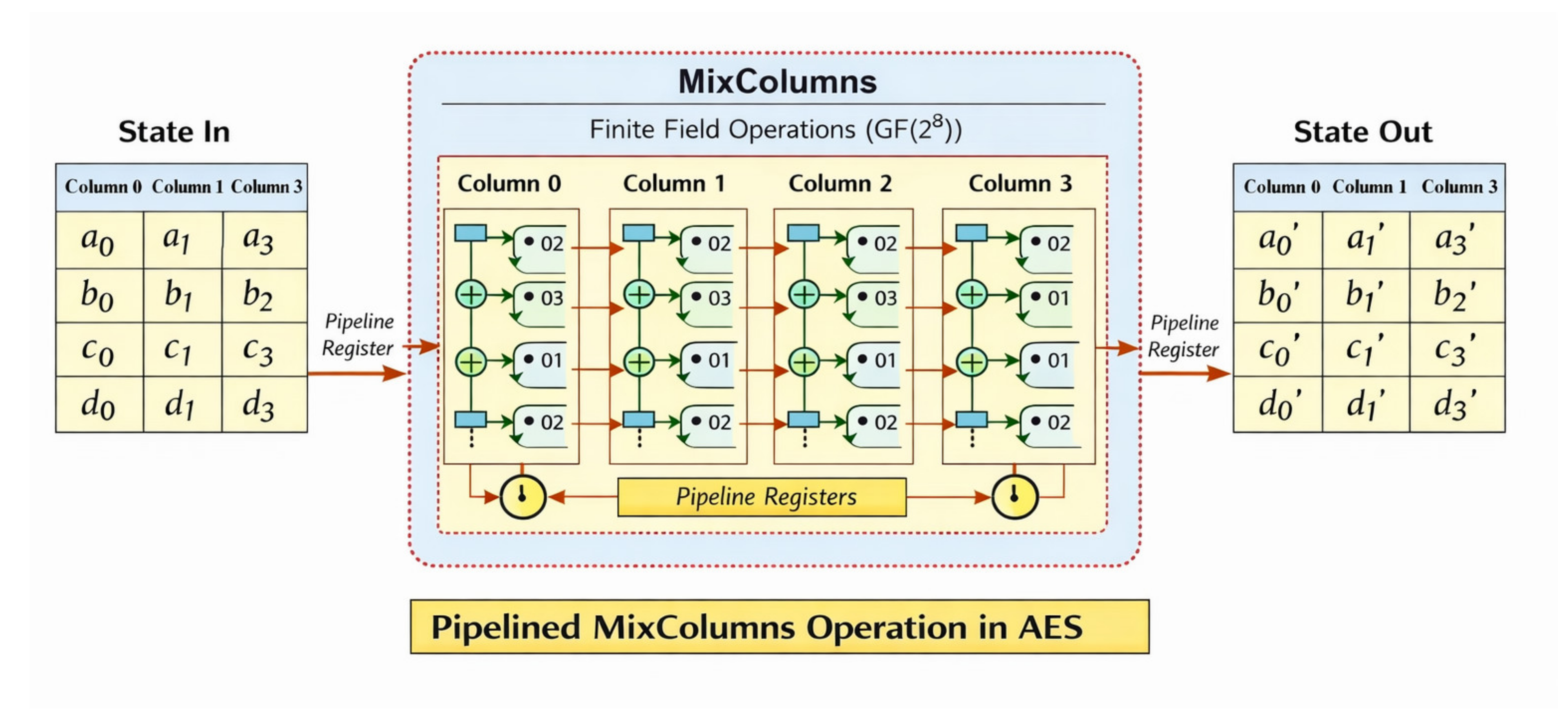
MixColumns: A linear mixing operation on each column: the four bytes of a column are treated as a polynomial over GF(28) and multiplied by a fixed MDS matrix. Each input byte thus influences all four output bytes, providing complete diffusion within the column.
AddRoundKey: A simple bitwise XOR of the state with the round’s 128-bit subkey. This injects key material each round.
These transformations are iterated for 9 full rounds. Finally, the 10th (last) round omits the MixColumns step. In other words, the cipher begins by XOR-ing the plaintext with the initial round key, then performs nine iterations of (Sub Bytes, Shift Rows, MixColumns, AddRoundKey), and concludes with a final SubBytes, ShiftRows, and AddRoundKey sequence. This well-defined loop structure (a “crypto-permutation” of S-boxes, shifts, linear mixing, and key additions) ensures high security: the S-box provides nonlinearity (confusion), while ShiftRows + MixColumns generate diffusion across bytes.
Note: All frequency values are expressed in hertz-based SI units, and all delay values are expressed in seconds
3.2. Pipelined AES Hardware Architecture
To accelerate AES in dedicated hardware (ASIC or FPGA), designers typically employ pipelined implementations that unroll the round loop and insert registers between stages. A fully unrolled AES-128 core can be arranged as a deep pipeline of stages, enabling a new plaintext block to enter each cycle [
14,
15]. In this design, one block per cycle after pipeline fill, assuming continuous input data and no pipeline stalls, the architecture produces one 128-bit ciphertext block per clock cycle at the output stage, while intermediate blocks simultaneously occupy different pipeline stages [
14].
where T denotes the throughput in bits per second and f_(clk) represents the clock frequency in hertz. At f_(clk) = 1.39 GHz, the achievable throughput is approximately 178 Gbps [
12]. In practice, the maximum achievable clock frequency is strongly dependent on the target technology, placement and routing constraints, and the depth of intra-round pipelining, and may be lower than the nominal value assumed in this example [
14,
15].
It should be noted that (1) represents the theoretical peak throughput, assuming a fully unrolled and fully inter-round-pipelined architecture with no pipeline stalls and continuous data availability.
The entire 10-round sequence is unrolled and partitioned into pipeline stages by inserting registers between rounds (or groups of rounds). This allows successive blocks to be processed in parallel across different rounds. For example, a fully inter-round-pipelined AES yields one block per cycle after the pipeline fill, dramatically increasing throughput.
Intra-round (Transformation-level) pipelining: Each round’s internal transformations can themselves be partitioned. For instance, the S-box computation, row shifts, and MixColumns logic may be split into sub-stages with registers in between. By pipelining within each round, the critical path is reduced to that of the slowest sub-transformation. In FPGAs or ASICs, this often means pipelining the SubBytes, ShiftRows, and MixColumns units so that no single stage is excessively long. Together with inter-round pipelining, this approach balances the logic and can allow much higher clock frequencies [
16].
While pipelining greatly raises throughput, it incurs performance trade-offs. The area overhead of extra registers is typically small relative to the entire logic, but each pipeline stage adds latency. Although deeply pipelined AES cores can achieve very high throughput, this comes at the cost of increased latency proportional to the pipeline depth. Consequently, such architectures are best suited for streaming or bulk-data encryption scenarios rather than latency-critical applications. However, the encryption of a single block then spans many clock cycles (equal to the number of pipeline stages), so end-to-end latency is high, as one study notes, “heavily pipelined configurations will have extremely long latencies when compared to the base iterative version of AES-128 [
14].” Designers must balance these factors: a fully pipelined design yields one block per cycle but may require ∼10 cycles of delay, whereas a non-pipelined loop has lower latency but much lower block throughput. In hardware cryptographic implementations, pipelining is favoured because modern ASICs and FPGAs have abundant registers and require extreme data rates (often multi-Gbps). Empirically, pipelined AES cores on FPGA/ASIC achieve tens of gigabits/sec of throughput by unrolling the rounds and inserting registers. In summary, pipelining in AES hardware leverages parallelism to maximise throughput at the expense of increased pipeline latency (and a modest register-area cost). Therefore, the choice of pipelining depth represents a design trade-off among throughput, latency, and area. While fully pipelined AES architectures maximise throughput, practical implementations must carefully balance these parameters based on application requirements and target hardware constraints. The overall AES encryption datapath is organised as a fully pipelined architecture.
Figure 2 shows the block-level architecture of the fully pipelined AES-128 encryption core, showing the sequential flow of SubBytes, ShiftRows, MixColumns, and AddRoundKey operations across multiple rounds with pipeline registers inserted to reduce the critical path.
3.3. Algorithmic Design and RTL Architecture of the Proposed AES-128 Core
3.3.1. AES Main Encryption Flow
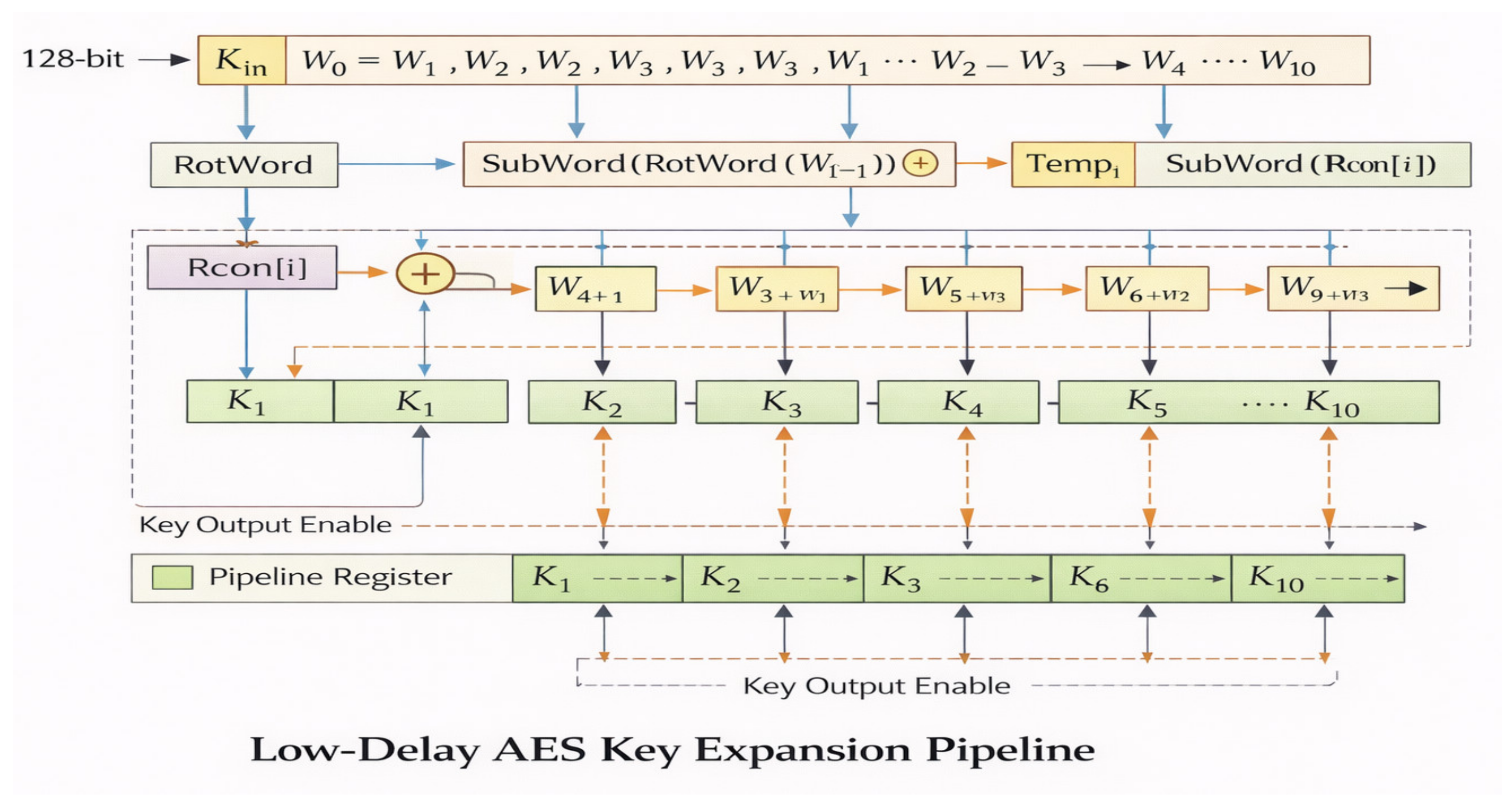
AES-128’s key expansion process derives eleven 128-bit round keys from the cipher key using RotWord, SubWord, and Rcon functions. The first four words are derived directly from the cipher key, with the remaining words being recursively computed using XOR-based transformations. The round keys are fed to each pipeline stage to ensure correctness in key alignment during the encryption process.
The overall functional flow of the proposed AES-128 encryption core is summarised in Algorithm 1.
| Algorithm 1: AES_Main Encryption Process |
Input: 128-bit plaintext P, 128-bit cipher key K
Output: 128-bit ciphertext C |
| 1. Generate round keys K0, K1, …, K10 using the AES-128 key expansion |
| 2. S ← AddRoundKey(P, K0) |
3. For i = 1 to 9 do
S ← AES_Round(S, Ki) |
| 4. C ← AES_FinalRound(S, K10) |
3.3.2. Key Expansion Architecture
AES-128 employs a 128-bit cipher key, which is expanded into 44 words, each of 32 bits (4 bytes), forming 11 round keys of 128 bits each [
17]. The expansion works as follows:
The first four words come directly from the original key.
For each new word
where
:
After all 44 words are generated, every four consecutive words form a complete 128-bit round key. In hardware, this logic is typically implemented within a dedicated key expansion module integrating SubWord, RotWord, and Rcon operations [
18]. Designers may choose to compute all keys ahead of time or generate keys on the fly each round [
19]. Since the operations are simple XOR and byte transformations, the module is compact and does not significantly impact timing. Verification typically involves comparing the generated keys with a reference software model.
Figure 3 illustrates the hardware architecture of the AES-128 key expansion module. The RotWord and SubWord transformations provide nonlinear key updates, while the injection of Rcon provides variation that depends on the rounds. The generated keys are then passed to the encryption datapath, which is pipelined.
The generation of round keys from the original cipher key follows the recursive AES key scheduling procedure, which is described in Algorithm 2.
For the case where i mod 4 = 0i\i mod 4 = 0 i mod 4 = 0, the word is computed as:
Algorithm 2 is implemented as a dedicated hardware key expansion module that supplies round keys to the encryption datapath either precomputed or on-the-fly.
| Algorithm 2: AES-128 Key expansion |
Input: 128-bit cipher key K
Output: Round keys K0, K1, …, K10 (each 128-bit) |
| 1. Initialise words w0, w1, w2, w3 from cipher key K |
2. For i = 4 to 43 do
If (i mod 4 = 0) then
wi ← wi–4 ⊕ SubWord(RotWord(wi–1)) ⊕ Rcon[i/4]
Else
wi ← wi–4 ⊕ wi–1 |
| 3. Group every four consecutive words to form round keys K0 to K10 |
| 4. Return all round keys |
3.3.3. Sub Byte
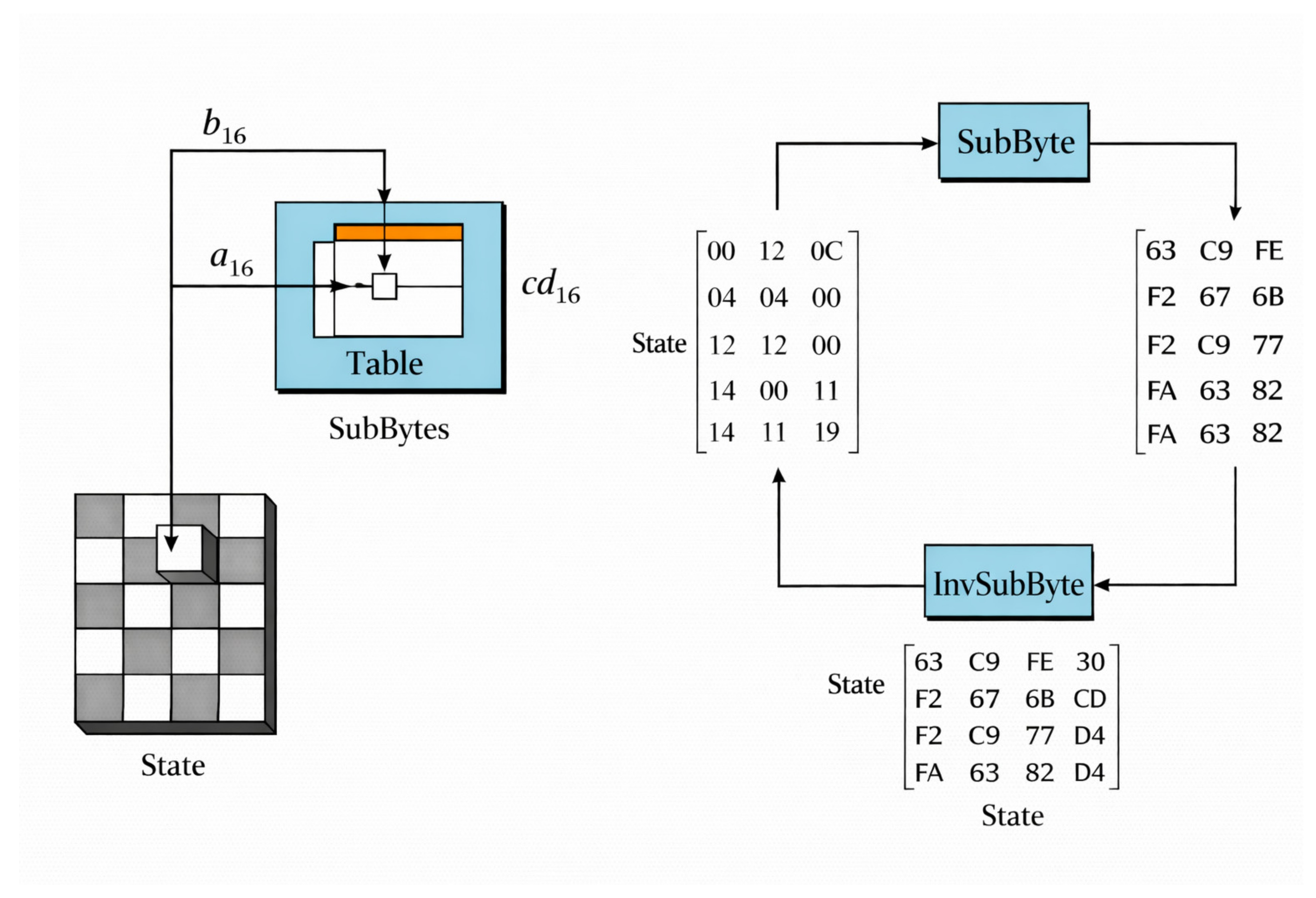
The SubBytes phase is responsible for the single nonlinear step in AES. In this phase, each byte of the 4 × 4 state matrix is substituted by another byte according to a predefined 256-element substitution table (S-box). SubBytes creates substantial confusion and makes sure that the result is a complex and nonlinear function of both the input and the key [
20].
The SubBytes stage is commonly implemented as a set of 16 parallel S-boxes in hardware, enabling processing of all 16 bytes of the 128-bit state in a single clock cycle [
21]. An S-box can be implemented as either (i) a small ROM-based lookup table or (ii) a combinational logic network built upon GF(2
8) operations [
22].
In this project, a ROM-based parallel architecture has been adopted, where 16 parallel S-boxes perform substitution in one clock cycle for all the bytes in the state. This implementation was chosen because of the simplicity and regularity of such an implementation as well as the high speed and suitability of the pipeline design [
23]. Compared to the combinational logic implementation, a ROM-based solution is faster and simpler to integrate into a design [
24], which is important when implementing AES into an ASIC.
As SubBytes consists only of combinational logic, it is easy to place it in a pipelined architecture without increasing latency [
25]. Parallelism enables the high throughput of the design and only moderate overhead in terms of area resources, creating a good compromise between the two aspects. For instance, the input byte 0x19 is replaced with the corresponding S-box value (e.g., 0xD4). This substitution is done independently for all 16 bytes in the state before the ShiftRows phase starts.
Figure 4 illustrates the SubBytes transformation, in which each byte of the AES state is replaced with a value from a nonlinear S-box, introducing confusion in the encryption process.
Algorithm 3 shows SubBytes replaces each byte of the AES state using a nonlinear S-box lookup.
It increases security by adding confusion and allows parallel hardware execution.
| Algorithm 3: AES SubBytes Transformation |
Input: 128-bit state array S
Output: Substituted state array S′ |
1. For i = 0 to 15 do
bi′ ← Sbox(bi) |
2. Combine all substituted bytes to form the new state:
S′ = {b0′, b1′, b2′, …, b15′} |
3. Return S′.
End |
3.3.4. Shift Rows
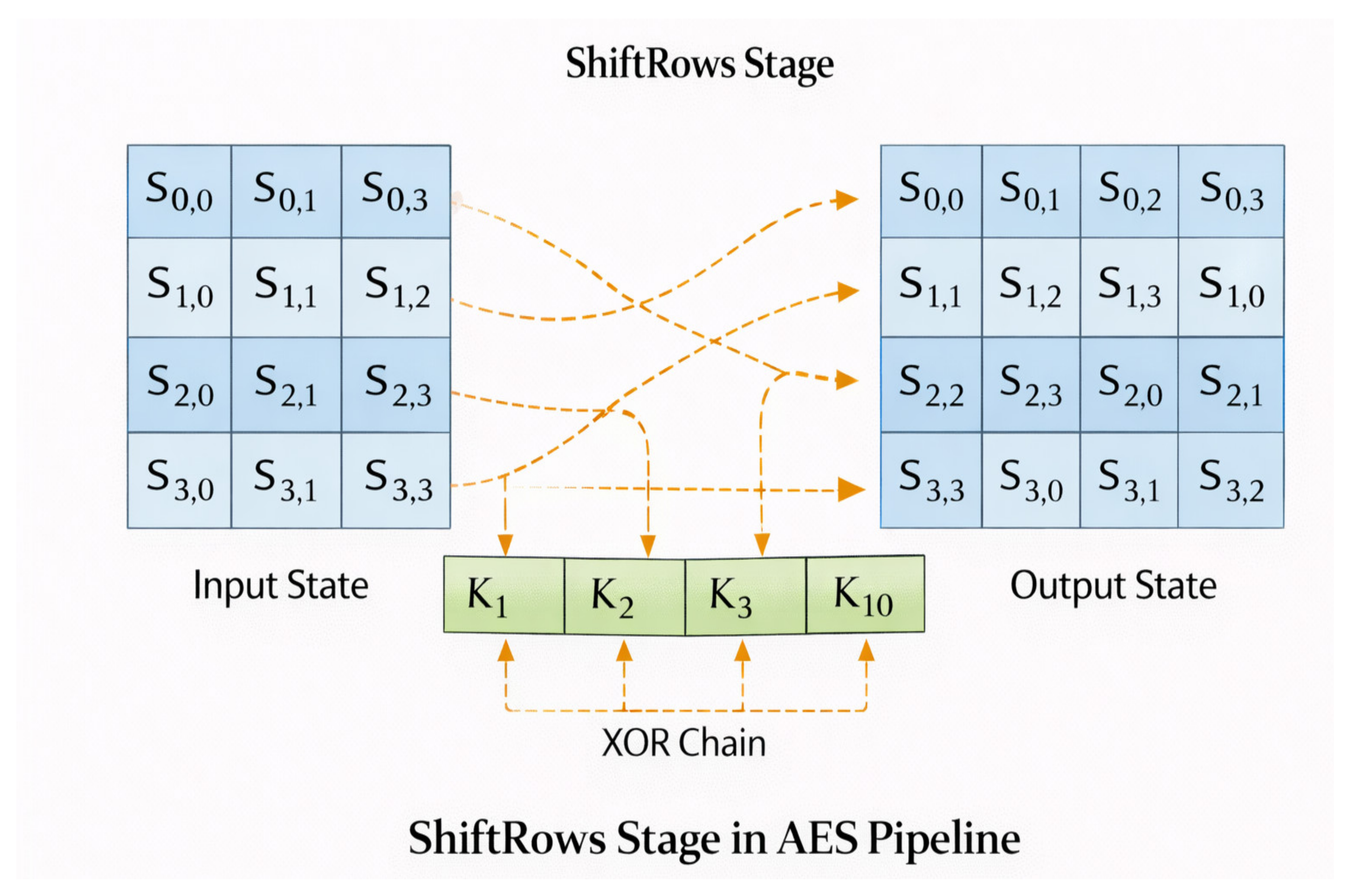
The transformation of ShiftRows enhances diffusion of AES; the rows of the state matrix are permuted in a cyclic manner [
26]. Considering that the state can be considered as a 4 × 4 byte array, the former row is not moved, and the other rows are moved to the left by one, two, and three-byte positions, respectively. This operation does not modify the bit patterns of the bytes; it just modifies their positions in the state.
The ShiftRows transformation redistributes bytes across columns; the distribution of the bytes into columns helps the further step of MixColumns to merge the data which was obtained in different columns. This communication triggers the propagation of variations of inputs to the entire state over several encryption steps, thus adding to the diffusion power of the cipher [
27].
From a hardware perspective, the ShiftRows operation is computationally efficient and can be implemented using simple wiring without additional logic. Because it only requires the repositioning of bytes, the operation can be realised by means of fixed wiring, without the need for arithmetic logic or memory access [
24]. Therefore, the module is entirely combinational and adds insignificant delay.
In a pipelined AES implementation, ShiftRows is generally inserted between the SubBytes and MixColumns steps, and it does not need a special pipeline register [
28]. Registers are placed around MixColumns or round boundaries instead to help satisfy timing constraints, and ShiftRows remain off-critical. This enables the entire AES round, including SubBytes, ShiftRows, MixColumns, and AddRoundKey, to be performed in an efficient manner in only one clock cycle.
Figure 5 also highlights that ShiftRows is purely a permutation-based operation, which enables an efficient hardware implementation using fixed wiring without additional logic overhead.
Algorithm 4 shows that ShiftRows cyclically shifts the rows of the AES state to provide diffusion between columns.
The operation only reorders byte positions, making it lightweight and efficient for hardware implementation.
| Algorithm 4: AES ShiftRows Transformation |
Input: 128-bit state array S
Output: Row-shifted state array S′ |
| 1. Arrange the input state S into a 4 × 4 byte matrix. |
2. Perform cyclic left shifts on each row:
Row 0 → no shift
Row 1 → shift left by 1 byte
Row 2 → shift left by 2 bytes
Row 3 → shift left by 3 bytes |
| 3. Rearrange the shifted bytes to form the new state S′. |
4. Return S′.
End |
3.3.5. Mix Column
The MixColumns transformation is the primary linear diffusion step of the AES round, combining the state bytes using finite field arithmetic over GF(2
8). One of the AES rounds is the MixColumns transformation that combines information at a bit level in the state. Under this operation, the columns of the 4 × 4 byte matrix are processed individually with the arithmetic of finite-field arithmetic on GF(2
8), resulting in outputs which are based on the four input states of the same column [
29].
Combined with the ShiftRows permutation, MixColumns is used to make sure that the data dependencies spread fast throughout the entire state over multiple rounds. The relationship facilitates the amplification of small changes in inputs so that the diffusion property of the cipher is enhanced and the avalanche effect that ensures the encryption is secure is achieved [
25].
From a hardware perspective, MixColumns is not as friendly as other AES transformations, because it is arithmetically complex. Constant multiplications required are usually implemented with XOR networks and conditioned shifts, which add significant combinational delay. Consequently, MixColumns can easily become a significant part of the critical path of the AES datapath [
27].
Figure 6 illustrates the column-wise diffusion process of the MixColumns transformation, highlighting how input bytes are linearly combined using Galois Field arithmetic.
The column-wise linear diffusion operation of AES is defined by the MixColumns transformation, which is described in Algorithm 5.
| Algorithm 5: MixColumns Transformation |
Input: 128-bit state S
Output: 128-bit transformed state S′
|
| 1. Divide S into four 32-bit columns C0, C1, C2, C3 |
2. For each column Ci do
Compute Ci′ using GF(28) multiplications by constants {02} and {03} |
| 3. Concatenate C0′, C1′, C2′, C3′ to form S′ |
| 4. Return S′ |
Algorithm 5 highlights the computational complexity of the MixColumns operation, which motivates the insertion of pipeline registers around this block to reduce the critical path delay.
3.4. Data Flow and Module Integration
The encryption process begins with the initial key encryption with the addition of RoundKey. Next, in rounds 1 to 9, the data is processed in the SubBytes, ShiftRows, Sequentially MixColumns, and AddRoundKey modules.
The 10th round skips the MixColumns step. The key expansion unit continuously provides the appropriate round keys. The round modules are linked in a successive way and with an enable and a clock timing operation by using gating logic. The modularity has the benefit of being easily verified and simplifies synthesis.
3.5. Pipelining Strategy
In order to support high-speed requirements, the design presents pipelining on two levels. Round-Level Pipelining Round registers are decoupled between rounds so that they can be used on multiple blocks at the same time.
By inserting pipeline registers around the MixColumns transformation, the critical path delay was reduced from 719 ps to 300 ps, allowing the design to achieve a maximum clock frequency of 1.39 GHz. All timing values are reported after post-synthesis static timing analysis.
Despite the introduction of additional pipeline registers, the area overhead remains moderate due to efficient module reuse.
4. Verification and Results
4.1. UVM-Based Verification Environment
The proposed AES-128 core was tested using a UVM-based environment that included a driver, monitor, scoreboard, and coverage collector. Over 1000 directed and constrained-random test cases were run, including corner cases such as all-zero and all-one inputs, as well as random key-data combinations. All AES transformations, such as SubBytes, ShiftRows, MixColumns, and AddRoundKey, were functionally covered to about 95%. Output comparison was performed using the scoreboard against a reference software AES golden model, and no mismatches were found. In addition, correctness was verified using standard AES known-answer test vectors (FIPS-197). Waveform analysis confirmed proper pipelining, datapath operation, and synchronisation of the key expansion stage. Assertion-based checks were also used to verify correct pipeline synchronisation and round-key alignment. Waveform analysis further confirmed proper pipelining and synchronisation between the datapath and key expansion stages.
4.2. Performance Comparison with Existing Works
We developed an AES-128 encryption core in SystemVerilog and synthesised it in an industrial ASIC design environment. The design was able to operate at a frequency of 1.39 GHz in a 65 nm technology. In the non-pipelined design, the critical path was shown to be 719 ps. By implementing the proposed pipelining scheme, especially in the MixColumns stage and at the boundaries of each round, the critical path delay was decreased to 300 ps. This is a more than two-fold improvement in timing with a negligible area increase. The overall area of the design (CADENCE Genus report) is around 327,836.520 µm2 silicon area and the design occupies approximately 327k standard cell equivalents. Although the design incorporates pipeline registers, the modular RTL design allows for efficient hardware mapping without replication of logic. From power analysis, it is apparent that the design strikes a reasonable compromise between speed and power. While the design is primarily targeted towards high-speed applications, switching activity remains stable even under post-synthesis conditions.
While many previous studies have focused on FPGA-based AES-128 designs or partial optimisation, this research offers a fully integrated pipelined AES-128 architecture, including RTL design, verification, synthesis, and performance analysis.
The performance comparison of the proposed AES-128 core with prior works is presented in
Table 3. To ensure a fair comparison, the reported implementations are categorised based on their hardware platform (ASIC or FPGA), and comparisons are interpreted accordingly.
As observed from
Table 3, most of the existing implementations are FPGA-based and exhibit limited frequency scaling. In contrast, the proposed design achieves a significantly higher operating frequency and reduced critical path delay. This demonstrates that the proposed architecture is better suited for high-performance ASIC-based cryptographic applications.
It is interesting to note that the comparison carried out in
Table 3 covers implementations using both FPGA and ASIC technologies. Therefore, the outcome is considered based on design trends such as critical path delay, maximum frequency, and design efficiency.
In particular, compared with the other ASIC-based AES-128 designs, the proposed work has a better timing performance and comparable area. This shows that the proposed intra-round and inter-round pipelining approach is effective for high-speed ASIC designs. A more rigorous comparison with closely related ASIC-based AES implementations is considered for future work.
4.3. Post-Synthesis Results
4.3.1. Timing Analysis
Table 4 illustrates the critical path timing analysis result after synthesis, in which the original datapath has a maximum combinational path of 719 ps, mostly caused by the MixColumns logic because of the GF(2
8) multiplier XOR-shift network. The MixColumns transformation was determined as the largest contributor to the critical path in the non-pipelined design (~719 ps). The critical path delay was minimised to approximately 300 ps by adding fine-grained pipeline registers around this point, reflecting a focused pipeline optimisation, as opposed to a more traditional homogeneous pipelining strategy. This targeted pipeline placement differentiates the proposed architecture from conventional fully pipelined AES designs, where registers are typically inserted only between rounds.
After the proposed pipelining scheme was applied to the datapath, the critical path was reduced to 300 ps. This confirms that the register insertion was performed in a non-redundant manner, which is essential in achieving ASIC-level timing closure without architectural over-engineering. The achieved path delay reduction (>2×) puts the engine into the multi-GHz domain of cryptographic accelerators, going beyond the iterative ASIC-based AES engines. As illustrated in
Table 4, the post-synthesis timing report highlights the critical path. As shown in
Table 4, the post-synthesis timing report confirms a maximum combinational delay of 300 ps, corresponding to a clock frequency of 1.39 GHz under typical process conditions.
Table 4 presents the post-synthesis timing results of the proposed AES-128 architecture, highlighting the reduction in critical path delay after pipelining.
As shown in
Table 4, the original datapath exhibits a critical path delay of 719 ps, primarily due to the MixColumns stage involving GF(2
8) arithmetic operations. After applying the proposed pipelining strategy, the critical path delay is reduced to 300 ps, enabling a maximum operating frequency of 1.39 GHz. This demonstrates that the pipelining approach effectively improves timing performance while maintaining efficient hardware utilisation. The post-synthesis timing report highlights the critical path, confirming a maximum combinational delay of 300 ps under typical process conditions.
It is necessary to note that the 300 ps reported is the lower combinational critical path delay that is obtained with balanced pipelining. The highest operating frequency of 1.39 GHz corresponds to a clock period of approximately 719 ps, as determined by post-synthesis timing analysis. This clock period has other timing limits like setup time, clock uncertainty and routing effects. Thus, the maximum achievable clock frequency is less than the maximum suggested by the critical path delay. The synthesis-reported delay of ~715 ps represents the effective clock period after timing closure, not the isolated combinational delay.
4.3.2. Hardware Resource Utilisation
Table 5 summarises the hardware resource utilisation of the proposed design in 65 nm CMOS technology.
The area is reported in terms of physical silicon area (µm
2), while the equivalent gate count is provided separately for design comparison. As shown in
Table 5, the proposed design efficiently utilises hardware resources with a total cell area of 327,836.520 µm
2 in 65 nm CMOS technology. The dominance of combinational logic is mainly due to the MixColumns and substitution operations. The pipelined architecture ensures efficient mapping without logic duplication, making the design suitable for high-performance ASIC implementations. It is noted that the 327k reported is in units of standard cell equivalents (gate count), but the value 327,836.520 µm 2 is the actual physical area of silicon that was obtained at the end of synthesis. The two metrics are distinct dimensions of the utilisation of hardware and are reported individually to enable a clear understanding. Reporting both gate count and physical area ensures reproducibility and fair comparison across different technology nodes.
4.3.3. Power Analysis
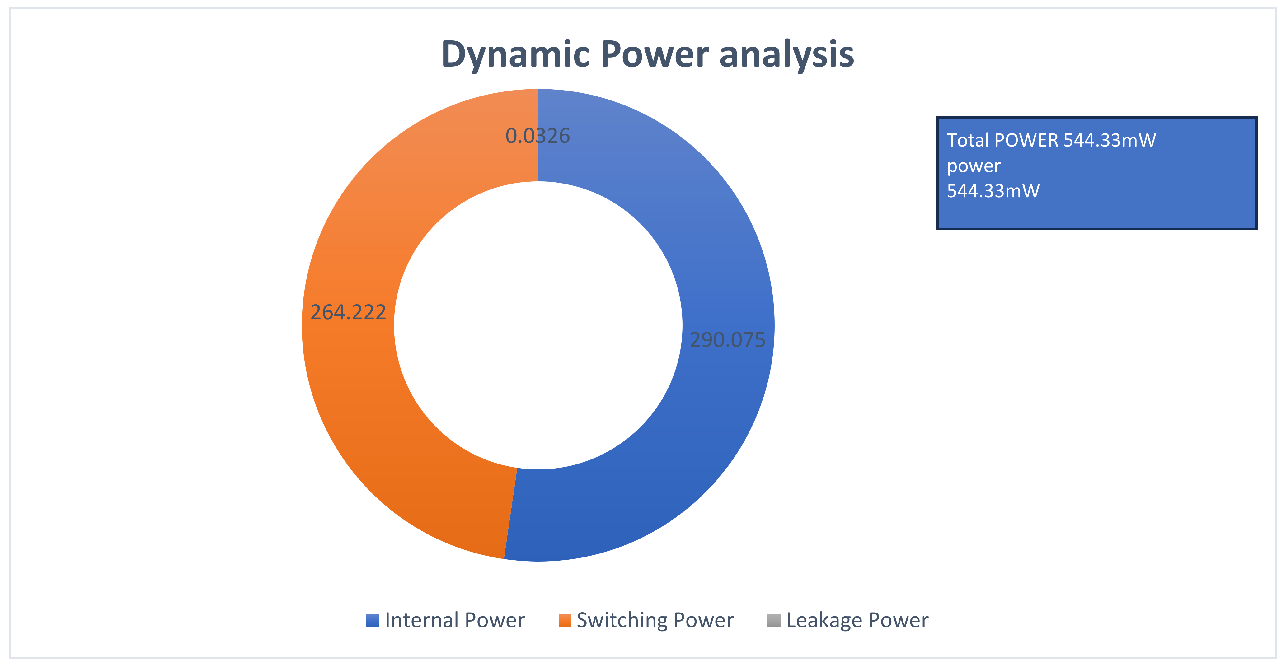
The post-synthesis dynamic power distribution of the proposed AES-128 architecture is summarised in
Table 6. The logic block has the largest internal power due to GF(2
8) arithmetic and XOR-based Mix Columns. The register and clock networks have moderate switching activity. The balanced pipeline placement suppresses glitches, which leads to stable dynamic power consumption across all pipeline stages. The synchronous pipelined structure also enhances the implementation robustness through long path glitch propagation reduction and unnecessary combinational switching activity minimisation by timing optimisation. Furthermore, the modular RTL architecture and the stage-wise verification process enable the problem of observability of faults when simulating and gate-level verifying the design, benefiting the reliable implementation of these cryptographic functions in an ASIC-based system. The above results demonstrate that the proposed architecture supports high operating frequency with manageable switching overhead. This power consumption is typical for high-frequency pipelined implementations of an ASIC, as switching activity and deep pipelining add to the dynamic power. The power consumption of 544.33 mW is consistent with high-frequency pipelined ASIC implementations, which makes it use more energy. This design is made for systems that need to send and receive information quickly and safely. It is meant for high-speed communication, so it uses more power than some other systems that are designed to use very little power. The amount of power it uses is similar to what other similar systems use, according to what has been reported. And this design prioritises speed. Additionally, the use of deep pipelining improves timing performance and throughput but introduces extra registers and clock-switching activity, which contribute to increased power consumption. This represents a well-known trade-off between speed and power in high-performance hardware design. The measured values of power are taken in a post-synthesis analysis in Cadence Genus under standard operating conditions. The analysis presupposes a nominal supply voltage and typical switching activity factors as given by the synthesis tool. Results are due to normal process corners and ambient temperature. The values of power reported are determined under vectorless estimation, which gives a rough estimate of the power consumption of the operating frequency.
Table 6 shows the detailed dynamic power distribution across different hardware components of the AES architecture.
Table 6 shows that the logic block consumes the highest power due to GF(2
8) calculations and intensive use of XOR gates in the MixColumns operation. The registers and clocking network consume moderately high switching power, but the memory and latch have a negligible impact on power consumption. The pipelined structure makes the design highly efficient at suppressing glitch propagation and thus consuming constant dynamic power throughout the pipelines.
It should be noted that the reported dynamic power consumption corresponds to a high-frequency operating condition (1.39 GHz) in a fully pipelined architecture. The design is primarily optimised for high-throughput applications rather than ultra-low-power scenarios. Therefore, although the power consumption is relatively higher, it is consistent with high-speed ASIC implementations. For low-power applications such as IoT systems, techniques such as clock gating, operand isolation, and resource sharing can be incorporated in future work to significantly reduce power consumption.
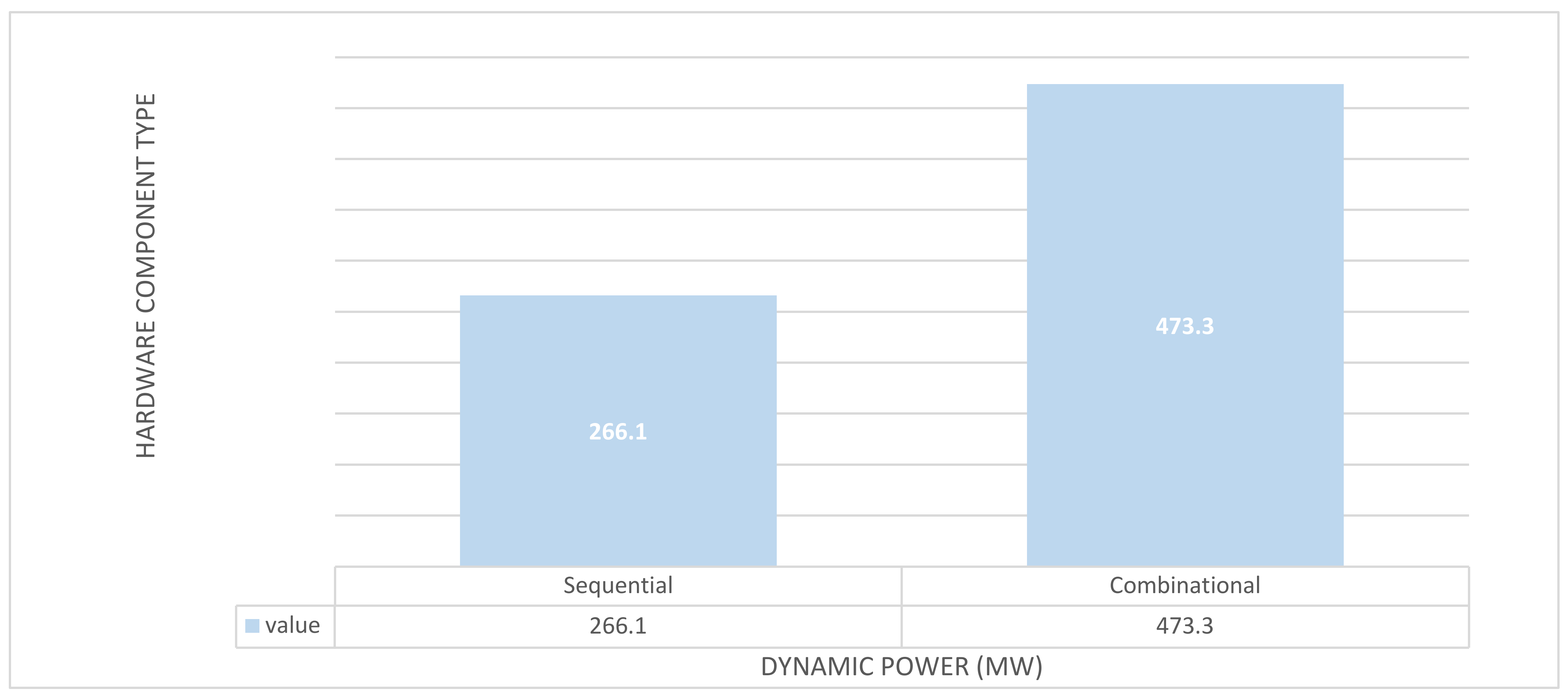
The comparison between sequential and combinational power components of the proposed AES-128 architecture is illustrated in
Figure 7.
The distribution of dynamic power consumption across different hardware components of the proposed AES-128 architecture is illustrated in
Figure 8.
4.3.4. Gate-Level Functional Verification
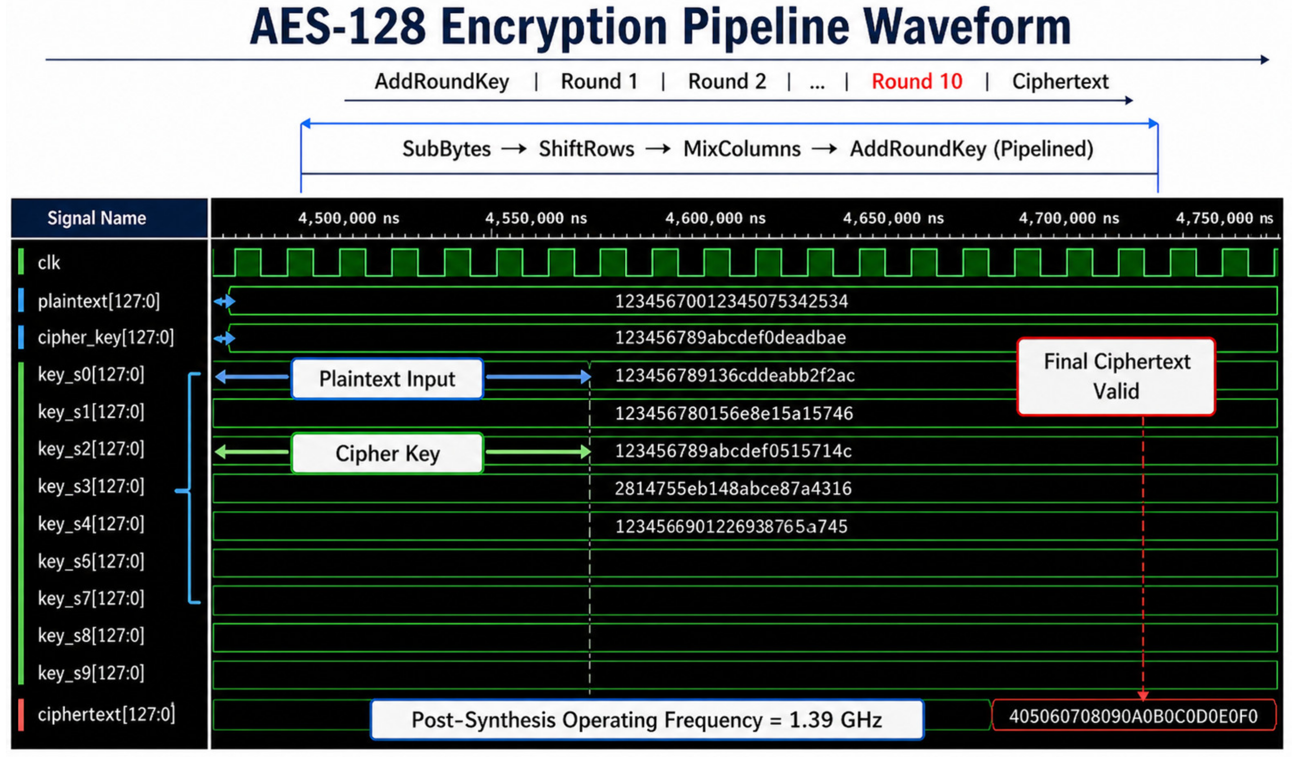
The detailed waveform analysis corresponding to the verification process is presented in
Figure 9.
Figure 9 shows that the plaintext message and key are fed into the AES-128 encryption core. The data goes through several pipelined stages associated with AES rounds such as SubBytes, ShiftRows, MixColumns, and AddRoundKey.
It is evident from the waveform that there is good pipelining with sequential generation of round results within successive clock cycles. After processing all rounds, the result will be the ciphertext, which is in line with the golden reference AES model. This is an indication that the AES design is correct.
Moreover, from the waveform analysis, it can be seen that the pipeline is working properly, as there is proper synchronisation between the datapath and key expansion stages.
4.3.5. Performance Summary of Proposed AES-128 Design
To provide a comprehensive evaluation of the proposed AES-128 core, key performance metrics, including throughput, latency, area, and energy efficiency, are summarised in
Table 7. These metrics are particularly important for pipelined architectures, where both throughput and latency must be considered.
5. Conclusions
This paper has described a highly pipelined and ASIC-friendly AES-128 encryption core design implemented in modular SystemVerilog, with UVM-based verification. The design adopts an efficient intra-round and inter-round pipelining approach to shorten the critical path delay of the MixColumns operation. The post-synthesis results and simulation results confirm a maximum possible clock frequency of 1.39 GHz when the Cadence Genus tool is used, with a critical path delay of about 300 ps, which demonstrates the effectiveness of the proposed architecture. Gate-level simulation and constrained-random verification ensure the design’s correctness through a comparison of the ciphertext results with the standard AES-128 test vectors.
The proposed design exhibits better timing results compared to previous FPGA and ASIC-based designs, with acceptable area and dynamic power consumption. But the current implementation is focused on achieving higher clock frequency, and does not include specific security measures against side-channel attacks such as differential power analysis (DPA) and fault injection, which could affect its use in security-sensitive applications. Moreover, low-power design techniques (e.g., clock gating, resource sharing) have been ignored in this design, leading to higher dynamic power consumption.
The design is realised in 65 nm CMOS technology, but the modular RTL architecture is scalable to smaller technology nodes (e.g., 45 nm and 28 nm). Since the design is RTL-based, it remains largely technology-independent and can be synthesised across different process nodes with appropriate standard-cell libraries, which will be investigated in future designs to assess performance, power and area trade-offs. Also, the proposed AES-128 core is inherently capable of processing each 128-bit plaintext block in the ECB mode as it is fully pipelined. In real cryptographic applications, the CBC operation can be implemented by means of external XOR feedback and control logic, which does not change the round structure of AES. The main emphasis of the present work is on optimisation of the forward encryption datapath, with the aim of achieving minimum critical path delay and maximum operating frequency. A unified encryption/decryption datapath would involve extra hardware for inverse transformation, reverse round-key scheduling, and extra control multiplexing and thus might increase the timing overhead and decrease the maximum frequency of the proposed ASIC-oriented pipelined architecture. The primary objective of this work is a high-speed ASIC-oriented AES implementation focusing on timing optimisation and throughput. Therefore, advanced side-channel protection mechanisms were not considered in the current design, and integrating low-power and side-channel attack countermeasure techniques (e.g., masking, hiding, and fault detection) remains an important direction to design secure and energy-efficient cryptographic systems. In contrast to other AES implementations, the proposed work presents a specific pipeline optimisation approach, based on the critical path associated with MixColumns, which leads to a considerable reduction of time.
Author Contributions
Conceptualisation, A.K. and S.M.; methodology, A.K.; software, A.K.; validation, A.K. and S.M.; formal analysis, A.K. and S.U.; investigation, S.M.; resources, S.M. and S.U.; data curation, A.K.; writing—original draft preparation, A.K.; writing—review and editing, S.M. and S.U.; visualisation, S.M.; supervision, S.M. and S.U. All authors have read and agreed to the published version of the manuscript.
Funding
This research is funded by Princess Nourah bint Abdulrahman University Researchers Supporting Project Number (PNURSP2026R79), Princess Nourah bint Abdulrahman University, Riyadh, Saudi Arabia.
Data Availability Statement
The data presented in this study are available within the article. No new external datasets were generated.
Acknowledgments
Authors are thankful to Princess Nourah bint Abdulrahman University Researchers Supporting Project Number (PNURSP2026R79), Princess Nourah bint Abdulrahman University, Riyadh, Saudi Arabia.
Conflicts of Interest
The authors declare no conflicts of interest.
Abbreviations
The following abbreviations are used in this manuscript:
| AES | Advanced Encryption Standard |
| ASIC | Application Specific Integrated Circuit |
| FPGA | Field Programmable Gate Array |
| UVM | Universal Verification Methodology |
| RTL | Register Transfer Level |
| CMOS | Complementary Metal Oxide Semiconductor |
| IoT | Internet of Things |
| S-Box | Substitution Box |
| BIST | Built In Self Test |
| DfT | Design for Testability |
| NIST | National Institute of Standards and Technology |
References
- Sheikhpour, S.; Mahani, A.; Bagheri, N. Reliable advanced encryption standard hardware implementation: 32-bit and 64-bit data-paths. Microprocess. Microsyst. 2021, 81, 103740. [Google Scholar] [CrossRef]
- Malal, A.; Tezcan, C. FPGA-friendly compact and efficient AES-like 8 × 8 S-box. Microprocess. Microsyst. 2024, 105, 105007. [Google Scholar] [CrossRef]
- Mestiri, H.; Kahri, F.; Bouallegue, B.; Machhout, M. A high-speed AES design resistant to fault injection attacks. Microprocess. Microsyst. 2016, 41, 47–55. [Google Scholar] [CrossRef]
- Bedoui, M.; Mestiri, H.; Bouallegue, B.; Hamdi, B.; Machhout, M. An improvement of both security and reliability for AES implementations. J. King Saud Univ.-Comput. Inf. Sci. 2022, 34, 9844–9851. [Google Scholar] [CrossRef]
- Nitaj, A.; Susilo, W.; Tonien, J. Enhanced S-boxes for the AES with maximal periodicity and better avalanche property. Comput. Stand. Interfaces 2024, 87, 103769. [Google Scholar] [CrossRef]
- Ahmad, N.; Hasan, S.M.R. A new ASIC implementation of an advanced encryption standard (AES) crypto-hardware accelerator. Microelectron. J. 2021, 117, 105255. [Google Scholar] [CrossRef]
- Soltani, A.; Sharifian, S. An ultra-high throughput and fully pipelined implementation of AES algorithm on FPGA. Microprocess. Microsyst. 2015, 39, 480–493. [Google Scholar] [CrossRef]
- Zhang, X.; Parhi, K.K. High-speed VLSI architectures for the AES algorithm. IEEE Trans. Very Large Scale Integr. (VLSI) Syst. 2004, 12, 957–967. [Google Scholar] [CrossRef]
- Lavanya, R.; Karpagam, M. Enhancing the security of AES through small scale confusion operations. Microprocess. Microsyst. 2020, 75, 103041. [Google Scholar] [CrossRef]
- FIPS PUB 197; Advanced Encryption Standard (AES). National Institute of Standards and Technology (NIST): Gaithersburg, MD, USA, 2001.
- Cheng, X.; Wang, H.; Luo, X.; Guan, Q.; Ma, B.; Wang, J. Re-Cropping Framework: A Grid Recovery Method for Quantization Step Estimation in Non-Aligned Recompressed Images. IEEE Trans. Circuits Syst. Video Technol. 2026, 36, 4771–4785. [Google Scholar] [CrossRef]
- Erkan, U.; Toktas, F.; Toktas, A.; Lai, Q.; Zhou, S.; Lin, Y.; Gao, S. Multi-layer and multi-directional image encryption algorithm based on hyperchaotic 3D Xin-She Yang map. Expert Syst. Appl. 2026, 304, 130808. [Google Scholar] [CrossRef]
- Abulibdeh, E.; Saleh, H.; Mohammad, B.; Alqutayri, M. Computational-Based Advanced Encryption Standard (AES) Accelerator. In 2023 International Conference on Microelectronics (ICM); IEEE: Abu Dhabi, United Arab Emirates, 2023; pp. 64–69. [Google Scholar] [CrossRef]
- Gokul, R.; Swarnalatha, A. Pipelined AES-128 encryption and decryption design using Verilog HDL. Int. J. Multidiscip. Res. (IJFMR) 2025, 7, 1–9. [Google Scholar] [CrossRef]
- Malal, A.; Tezcan, C. First fully pipelined high throughput FPGA implementation of wider AES. Res. Sq. 2025. [Google Scholar] [CrossRef]
- Ajmi, H.; Zayer, F.; Fredj, A.H.; Belgacem, H.; Mohammad, B.; Werghi, N.; Dias, J. Efficient and lightweight in-memory computing architecture for hardware security. J. Parallel Distrib. Comput. 2024, 190, 104898. [Google Scholar] [CrossRef]
- Azzouzi, O.; Anane, M.; Ghanem, M.C.; Himeur, Y.; Wojtczak, D. Flexible and area-efficient codesign implementation of AES on FPGA. Cryptography 2025, 9, 78. [Google Scholar] [CrossRef]
- Selvapriya, E.S.; Suganthi, L. Design and implementation of low power AES cryptocore utilizing dynamic pipelined asynchronous model. Integration 2023, 93, 102057. [Google Scholar] [CrossRef]
- Pradeep, A.; Mohanty, V.; Subramaniam, A.M.; Rebeiro, C. Revisiting AES SBox Composite Field Implementations for FPGAs. IEEE Embed. Syst. Lett. 2019, 11, 85–88. [Google Scholar] [CrossRef]
- Rashmi, R.; Mohan, A. Implementation of AES S-Boxes using combinational logic. In 2008 IEEE International Symposium on Circuits and Systems (ISCAS); IEEE: Seattle, WA, USA, 2008; pp. 3294–3297. [Google Scholar] [CrossRef]
- Lin, S.-H.; Lee, J.-Y.; Chuang, C.-C.; Lee, N.-Y.; Chen, P.-Y.; Chin, W.-L. Hardware implementation of high-throughput S-box in AES. IEEE Access 2023, 11, 59049–59058. [Google Scholar] [CrossRef]
- Bazgir, O.; Gali, S.; Nikoubin, T. Area-power and energy efficient S-box in AES. In GLSVLSI 2024 Proceedings; ACM: New York, NY, USA, 2024; pp. 263–267. [Google Scholar] [CrossRef]
- Sumio, M.; Akashi, S. An Optimized S-Box Circuit Architecture for Low Power AES Design. In Cryptographic Hardware and Embedded Systems—CHES 2002; Springer: Berlin/Heidelberg, Germany, 2002; Volume 2523, pp. 172–186. [Google Scholar] [CrossRef]
- Thanikodi, M.K. AES algorithm for power-efficient and high-speed applications. Wirel. Pers. Commun. 2025, 140, 225–239. [Google Scholar] [CrossRef]
- EL Makhloufi, A.; EL Adib, S.; Raissouni, N. Hardware pipelined AES architecture for satellite data. e-Prime 2024, 8, 100548. [Google Scholar] [CrossRef]
- Yu, F.; Xu, S.; Xiao, X.; Yao, W.; Huang, Y.; Cai, S.; Li, Y. Dynamic analysis and FPGA implementation of chaotic system. Integration 2024, 96, 102129. [Google Scholar] [CrossRef]
- Prayitno, R.H.; Latifah; Sudiro, S.A.; Madenda, S.; Harmanto, S. A modified MixColumn-InversMixColumn in AES algorithm suitable for hardware implementation using FPGA device. Commun. Sci. Technol. 2023, 8, 198–207. [Google Scholar] [CrossRef]
- Visconti, P.; Capoccia, S.; Venere, E.; Velázquez, R.; Fazio, R.d. 10 Clock-Periods Pipelined Implementation of AES-128 Encryption-Decryption Algorithm up to 28 Gbit/s Real Throughput by Xilinx Zynq UltraScale+ MPSoC ZCU102 Platform. Electronics 2020, 9, 1665. [Google Scholar] [CrossRef]
- Mohamed, H.A.A.; Yakout, M.A. An Efficient AES Design and Implementation Using FPGA. Int. J. Emerg. Sci. Eng. 2025, 13, 21–26. [Google Scholar] [CrossRef]
- Liu, Q.; Xu, Z.; Yuan, Y. High Throughput and Secure Advanced Encryption Standard on Field Programmable Gate Array with Fine Pipelining and Enhanced Key Expansion. IET Comput. Digit. Tech. 2015, 9, 175–184. [Google Scholar] [CrossRef]
- Dixit, N.K. Advanced FPGA Implementation of AES Algorithm. Int. J. Emerg. Trends Eng. Res. 2021, 9, 4. [Google Scholar] [CrossRef]
- Algredo-Badillo, I.; Ramírez-Gutiérrez, K.A.; Morales-Rosales, L.A.; Pacheco Bautista, D.; Feregrino-Uribe, C. Hybrid Pipeline Hardware Architecture Based on Error Detection and Correction for AES. Sensors 2021, 21, 5655. [Google Scholar] [CrossRef]
Figure 1.
AES-128 encryption process showing 4 × 4 state matrix representation and round transformations.
Figure 1.
AES-128 encryption process showing 4 × 4 state matrix representation and round transformations.
Figure 2.
Fully Unrolled AES-128 Pipeline Showing Inter-Round Register Placement.
Figure 2.
Fully Unrolled AES-128 Pipeline Showing Inter-Round Register Placement.
Figure 3.
Hardware architecture of the AES-128 key expansion module showing RotWord, SubWord, and Rcon operations.
Figure 3.
Hardware architecture of the AES-128 key expansion module showing RotWord, SubWord, and Rcon operations.
Figure 4.
SubBytes operation showing nonlinear byte substitution using the AES S-box.
Figure 4.
SubBytes operation showing nonlinear byte substitution using the AES S-box.
Figure 5.
ShiftRows operation.
Figure 5.
ShiftRows operation.
Figure 6.
MixColumns transformation showing column-wise diffusion using Galois Field arithmetic.
Figure 6.
MixColumns transformation showing column-wise diffusion using Galois Field arithmetic.
Figure 7.
Sequential vs. Combinational Power.
Figure 7.
Sequential vs. Combinational Power.
Figure 8.
Dynamic Power Distribution Across Hardware Components of the Proposed AES-128 Architecture.
Figure 8.
Dynamic Power Distribution Across Hardware Components of the Proposed AES-128 Architecture.
Figure 9.
Gate-level simulation waveform of the proposed AES-128 pipelined encryption core showing plaintext input, key expansion, round transformations, and final ciphertext generation.
Figure 9.
Gate-level simulation waveform of the proposed AES-128 pipelined encryption core showing plaintext input, key expansion, round transformations, and final ciphertext generation.
Table 1.
Summary of Existing AES-128 Hardware Implementations and Limitations.
Table 1.
Summary of Existing AES-128 Hardware Implementations and Limitations.
| Year | Platform | Focus | Key Technique (s) | Max Frequency |
|---|
| 2019 | FPGA | High throughput | Loop unrolling with deep pipelining | 500 MHz |
| 2020 | FPGA | Area minimization | Iterative AES-128 architecture | 800 MHz |
| 2021 | ASIC | DfT/BIST | On-chip BIST for AES processor | 700 MHz |
| 2021 | FPGA | Low-area/high-speed | Resource sharing and RTL optimisation | 650 MHz |
| 2021 | ASIC | Compact IoT core | 8-bit datapath AES | 400 MHz |
| 2021 | Mixed HW | Reliability | Hybrid pipeline with error detection | – |
| 2022 | General HW | Security | Hardened AES techniques | – |
| 2022 | ASIC/FPGA | Area efficiency | Composite-field S-Box design | 750 MHz |
| 2023 | ASIC | Ultra-low power | Energy-optimised AES core | 300 MHz |
| 2024 | ASIC (65 nm) | Compact S-Box | Walsh–Hadamard-based S-Box | – |
Table 2.
Comparative Evaluation of AES-128 and Chaos-Based Multimedia Encryption Frameworks in Terms of Hardware Feasibility, Timing Optimisation, and Computational Complexity.
Table 2.
Comparative Evaluation of AES-128 and Chaos-Based Multimedia Encryption Frameworks in Terms of Hardware Feasibility, Timing Optimisation, and Computational Complexity.
| Evaluation Metric | Proposed AES-128 ASIC | EAS | 3D-NDHC | MLMD-IE | Re-Cropping Framework |
|---|
| Application Domain | Secure communication | Video encryption | Image encryption | Image encryption | Image forensics |
| Encryption Structure | SPN-based AES rounds | Temporal chaotic segmentation | Dynamic 3D S-box | Multi-layer diffusion | JPEG grid recovery |
| Security Mechanism | Deterministic substitution–permutation | Chaotic neuron map | Hyperchaotic diffusion | Hyperchaotic multidirectional diffusion | Quantisation analysis |
| Computational Complexity | Moderate | High | High | High | Moderate |
| Pipeline Suitability | High | Limited | Limited | Limited | Not targeted |
| ASIC Orientation | Yes | No | No | No | No |
| Timing Optimisation | Balanced intra-round and inter-round pipelining | Not reported | Not reported | Not reported | Not applicable |
| Evaluation Basis | ASIC timing + UVM | Statistical randomness | Entropy + Lyapunov | NPCR/UACI | Quantisation recovery |
| Post-Synthesis Metrics | 1.39 GHz, 300 ps | Not reported | Not reported | Not reported | Not reported |
| Verification/Evaluation Style | UVM + Cadence Genus ASIC evaluation | Statistical security and randomness analysis | Entropy, Lyapunov exponent, and cryptanalysis analysis | Entropy, NPCR, UACI, and correlation analysis | JPEG quantisation and forensic analysis |
| Hardware Implementation Focus | ASIC-oriented high-speed encryption | Software-oriented multimedia encryption | Multimedia privacy protection | Multimedia image encryption | Image forensic recovery |
| Main Complexity Source | MixColumns critical path | Chaotic sequence generation | Dynamic hyperchaotic S-box operations | Multi-directional recursive diffusion | DCT grid recovery and estimation |
| Throughput Orientation | High-throughput hardware architecture | Resource-efficient video protection | Security-oriented image encryption | Multi-layer security-oriented encryption | Forensic reconstruction framework |
| Timing Closure Support | Yes | No | No | No | No |
Table 3.
Performance Comparison of the Proposed AES-128 Core with Prior Works.
Table 3.
Performance Comparison of the Proposed AES-128 Core with Prior Works.
| Work (Year) | Parameter |
|---|
| Platform | Max Frequency | Delay | Area Utilization | Remark |
|---|
| Liu et al. (2015) [30] | FPGA | 501 MHz | 2 ns | High LUT usage | High throughput but FPGA-only |
| Dixit et al. (2021) [31] | FPGA | 813 MHz | 1.2 ns | Medium | Focus on pipelining |
| Ahmad and Hasan.(2021) [6] | ASIC | 100 MHz | 10 ns | Compact | Low area, modest speed |
| Algredo-Badillo et al. (2021) [32] | HW Arch. | – | – | Medium | Reliability-focused design |
| Proposed Work | ASIC | 1.39 GHz | 300 ps (pipelined) | 327k | High performance, ASIC-ready |
Table 4.
Synthesis Results of AES Encryption Design Using Cadence Genus.
Table 4.
Synthesis Results of AES Encryption Design Using Cadence Genus.
| AES Encryption Design | Parameter |
|---|
| Maximum Frequency | 1.39 GHz |
| Critical Path | Start-point: r4_a2_data_out_reg[110]/CK
End-point: r5_a1_s_data_out_reg[100]/D |
| Delay (Non pipeline) | 719 ps |
| Delay (Pipeline) | 300 ps |
Table 5.
Area Utilisation Analysis.
Table 5.
Area Utilisation Analysis.
| Parameter | Value |
|---|
| Technology | 65 nm CMOS |
| Total cell area | 327,836.520 µm2 |
| Design type | Fully Pipelined AES-128 |
| Dominant resource | Combinational Logic |
Table 6.
Dynamic Power Analysis.
Table 6.
Dynamic Power Analysis.
| Category | Leakage (mW) | Internal (mW) | Switching (mW) |
|---|
| Memory | 0.000 | 0.000 | 0.000 |
| Register | 0.0037 | 80.555 | 12.869 |
| Latch | 0.000 | 0.000 | 0.000 |
| Logic | 0.0289 | 209.520 | 251.353 |
| Bbox/Clock/Pad/PM | 0.000 | 0.000 | 0.000 |
| Total | 0.0326 | 290.075 | 264.222 |
Table 7.
Summary of Proposed AES-128 Design.
Table 7.
Summary of Proposed AES-128 Design.
| Metric | Value |
|---|
| Clock Frequency | 1.39 GHz |
| Throughput | 178 Gbps |
| Latency | 11 clock cycles |
| Cycles to First Output | 11 cycles |
| Architecture | Fully pipelined (1 block/cycle) |
| Area | 327,836 µm2 |
| Power | 544.33 mW |
| Energy per bit | ~3.05 pJ/bit |
| Area Efficiency | ~543 Mbps/µm2 |
| Disclaimer/Publisher’s Note: The statements, opinions and data contained in all publications are solely those of the individual author(s) and contributor(s) and not of MDPI and/or the editor(s). MDPI and/or the editor(s) disclaim responsibility for any injury to people or property resulting from any ideas, methods, instructions or products referred to in the content. |