Article

Machine Learning Framework for Automated Transistor-Level Analogue and Digital Circuit Synthesis

by
Rajkumar Sarma
1,2,*,
Dhiraj Kumar Singh
1,
Moataz Kadry Nasser Sediek
1 and
Conor Ryan
1,*
1
Biocomputing and Development Systems (BDS) Group, Computer Science and Information Systems (CSIS) Department, University of Limerick, V94 T9PX Limerick, Ireland
2
Department of Electrical and Electronic Engineering, School of Engineering, University of Galway, H91 TK33 Galway, Ireland
*
Authors to whom correspondence should be addressed.
Symmetry 2025, 17(12), 2169; https://doi.org/10.3390/sym17122169
Submission received: 27 October 2025 / Revised: 10 December 2025 / Accepted: 10 December 2025 / Published: 17 December 2025
(This article belongs to the Special Issue Symmetry/Asymmetry in Evolutionary Algorithms)

Abstract

Transistor-level Integrated Circuit (IC) design is fundamental to modern electronics, yet it remains one of the most expertise-intensive and time-consuming stages of chip development. As circuit complexity continues to rise, the need to automate this low-level design process has become critical to sustaining innovation and productivity across the semiconductor industry. This study presents a fully automated methodology for transistor-level IC design using a novel framework that integrates Grammatical Evolution (GE) with Cadence SKILL code. Beyond automation, the framework explicitly examines how symmetry and asymmetry shape the evolutionary search space and resulting circuit structures. To address the time-consuming and expertise-intensive nature of conventional integrated circuit design, the framework automates the synthesis of both digital and analogue circuits without requiring prior domain knowledge. A specialised attribute grammar (AG) evolves circuit topology and sizing, with performance assessed by a multi-objective fitness function. Symmetry is analysed at three levels: (i) domain-level structural dualities (e.g., NAND/NOR mirror topologies and PMOS/NMOS exchanges), (ii) objective-level symmetries created by logic threshold settings, and (iii) representational symmetries managed through grammatical constraints that preserve valid connectivity while avoiding redundant isomorphs. Validation was carried out on universal logic gates (NAND and NOR) at multiple logic thresholds, as well as on a temperature sensor. Under stricter thresholds, the evolved logic gates display emergent duality, converging to mirror-image transistor configurations; relaxed thresholds increase symmetric plateaus and slow convergence. The evolved logic gates achieve superior performance over conventional Complementary Metal–Oxide–Semiconductor (CMOS), Transmission Gate Logic (TGL), and Gate Diffusion Input (GDI) implementations, demonstrating lower power consumption, a reduced Power–Delay Product (PDP), and fewer transistors. Similarly, the evolved temperature sensor exhibits improved sensitivity, reduced power, and Integral Nonlinearity (INL), and a smaller area compared to the conventional Proportional to Absolute Temperature (PTAT) or “gold” circuit, without requiring resistors. The analogue design further demonstrates beneficial asymmetry in device roles, breaking canonical structures to achieve higher performance. Across all case studies, the evolved designs matched or outperformed their manually designed counterparts, demonstrating that this GE-based approach provides a scalable and effective path toward fully automated, symmetry-aware integrated circuit synthesis.

1. Introduction

Integrated Circuit (IC) design is the process of translating conceptual system requirements into a functional, manufacturable silicon chip by organising transistors and passive elements into meaningful circuits. A central challenge, particularly relevant to this work, is the automation of transistor-level analogue and digital circuit synthesis, where the design space is highly nonlinear, symmetry-rich, and tightly coupled to device physics. Traditional tools such as LTspice (v26.0.0, Analog Devices, Inc., Wilmington, MA, USA) and GNU Octave (v10.3.0, Free Software Foundation, Boston, MA, USA) provide reliable simulation and numerical analysis capabilities, but they do not perform structural circuit synthesis; instead, they operate as evaluation back ends and require manually created circuit topologies. Consequently, the core research problem addressed in this paper is how to automatically construct circuit topologies and device sizing using Machine Learning (ML) and evolutionary techniques. In today’s semiconductor industry, whether in smartphones, autonomous vehicles, edge Artificial Intelligence (AI) devices, or data centres, demand for highly optimised Application-Specific Integrated Circuits (ASICs) makes progress in such automation a critical driver of innovation and competitiveness.
Although often part of the same chip, analogue and digital IC design differ fundamentally in objectives and methodology [1]. Digital design operates on discrete binary signals, emphasising logical correctness, clock timing, and scalability, typically via automated flows using Hardware Description Languages (HDLs). Analogue design, by contrast, deals with continuous-time signals and relies heavily on subtle control of parameters such as gain, noise, linearity, and power. It resists full automation and requires significant designer expertise. At the transistor level, these differences are pronounced: analogue design involves current mirrors, biasing networks, and amplifiers with fine-grained control, while digital design focuses on optimising standard cells, Static Random Access Memory (SRAM) bit cells, and timing paths. Across both domains, symmetry plays a pivotal role, whether in differential pairs, matched transistors, or logic dualities such as NAND/NOR—defining how circuits balance performance and robustness.
Transistor-level IC design provides deep visibility and control, allowing designers to directly manipulate circuit behaviour based on semiconductor physics and layout interactions [2]. This approach is indispensable in analogue blocks, where performance often hinges on mismatch, parasitics, and temperature sensitivity. In digital domains, it is less common for complete systems, but it remains crucial for high-speed datapaths, low-power cells, or when synthesis tools fall short. The ability to custom-tailor these critical elements enables performance and efficiency often beyond what HDL-based design alone can deliver. However, the same design flexibility introduces large spaces of structurally symmetric but functionally equivalent solutions, making manual exploration both inefficient and prone to error.
This approach, however, faces challenges. As technology nodes continue to shrink, variations due to Process, Voltage, and Temperature (PVT) grow severe, and phenomena such as short-channel effects, leakage, and electromigration increasingly dominate circuit behaviour [3,4]. Robust performance across corners requires extensive simulation, tighter margins, and careful layout to minimise parasitic impacts [2]. Analogue design remains largely handcrafted, with layout parasitics and matching constraints adding further complexity. Combined with time-to-market pressure, full custom transistor-level design is both time-consuming and resource-intensive.
Despite these hurdles, transistor-level design offers unmatched advantages. It enables non-standard topologies and tighter area and power budgets and pushes performance limits, especially when synthesised components cannot meet demanding specifications. In both analogue and digital circuits, custom transistor-level work opens design spaces inaccessible to automated flows. Hybrid logic approaches—including Complementary Metal–Oxide–Semiconductor (CMOS) [5], Pass-Transistor Logic (PTL) [6], Gate Diffusion Input (GDI) [7], Transmission Gate Logic (TGL) [8], and dynamic logic [9]—show promise but still rely on low-level tuning to reach their potential. These diverse circuit families also exhibit rich symmetry structures (e.g., complementary pull-up/pull-down networks), which can either simplify optimisation or conceal equivalences that mislead search algorithms.
Human intuition remains a defining asset. While HDL-driven synthesis abstracts much of the process, transistor-level design depends on the designer’s skill in selecting topologies, sizing transistors, choosing operating points, and orchestrating layouts [10]. Analogue design in particular is shaped by empirical knowledge, heuristics, and a deep understanding of circuit interaction [11]. These decisions often reflect years of experience but also introduce limitations, such as bias, overfitting to familiar patterns, and difficulty scaling to complex designs. To achieve robust IC development at scale, verification, statistical methods, and intelligent automation must augment intuition. Evolutionary approaches, especially those that can detect or exploit underlying symmetries, offer a principled route toward that goal.
Grammatical Evolution (GE) [12] is an Evolutionary Algorithm (EA) that generates programs or expressions via a genotype-to-phenotype mapping based on a formal grammar. The grammar, typically defined in Backus–Naur Form (BNF), dictates valid solution structures, ensuring syntactic correctness during the evolution process. A fitness function then evaluates performance with respect to single or multiple objectives. This grammar-driven evolution, combined with fitness-based selection, makes GE a powerful tool for automated problem-solving. Within this context, symmetry manifests at three levels: (i) Representational: Through grammar rules that define equivalent syntactic forms. (ii) Domain: Through physically symmetric circuit topologies. (iii) Objective: Through fitness functions that reward balanced trade-offs. Understanding and managing these forms of symmetry is key to efficient evolutionary search.
In this work, we apply GE to synthesise transistor-level circuits by generating SKILL (Cadence Design Systems, Inc., San Jose, CA, USA) code, the scripting language of Virtuoso. Our approach supports both analogue and digital domains through separate grammars and fitness functions, with attribute grammars (AGs) used to incorporate semantic constraints for context-aware synthesis. We also examine how symmetry and asymmetry emerge during evolution, how logic threshold objectives induce or break equivalence between circuit families, and how grammar design can preserve necessary invariants while pruning redundant isomorphs.
We address the following research questions:
RQ1.
How effectively can GE generate functional transistor-level circuit designs while recognising and exploiting domain-level symmetries?
RQ2.
What is the impact of multi-objective evaluation and objective-induced symmetries (e.g., logic thresholds) on optimisation dynamics and the emergence or breaking of symmetric circuit forms?
RQ3.
Can the proposed automated system consistently generate competitive or superior analogue/digital circuits by balancing symmetry preservation and asymmetry-driven innovation across technology nodes?
SKILL provides the interface through which evolved circuits are instantiated, simulated, and evaluated in Cadence tools. By generating SKILL programs directly, our framework integrates tightly with existing Electronic Design Automation (EDA) workflows.
The remainder of this paper is organised as follows. Section 2 and Section 3 review related work in automated circuit design, GE, and Cadence SKILL. Section 4 describes the proposed methodology, including grammar design, fitness evaluation, and the simulation framework. Section 5 presents the experimental setup and results. Section 6 discusses the findings with respect to the research questions, and Section 7 concludes this paper.

2. Evolutionary Algorithm (EA)

 EAs are population-based stochastic optimisation techniques inspired by natural selection [13]. They evolve a population of candidate solutions through variation operators such as crossover and mutation, guided by a fitness function. Because they can explore large, complex search spaces without gradient information, EAs are widely applied in domains where analytical optimisation is infeasible.
One of the earliest and most widely used EAs is the Genetic Algorithm (GA) [14], which encodes solutions as fixed-length binary or real-valued strings. Over successive generations, selection and variation drive populations toward high-fitness solutions. While effective, GAs operate on abstract parameter spaces and are not directly suited for structural representations such as circuits or programs.
 Genetic Programming (GP) [15] extends this framework by evolving tree-based executable structures composed of functions and terminals. It has been successfully applied to symbolic regression, program synthesis, and control. However, its lack of a clear separation between genotype (encoding) and phenotype (expressed solution) can hinder scalability and control in structured domains such as hardware and circuit design. ge

2.1. Grammatical Evolution (GE)

GE [12] is a population-based search method for function approximation. It iteratively explores the genotype space and identifies phenotypes that better satisfy the objective. Following the classical ( μ + λ ) evolutionary strategy, GE maintains a population of candidate solutions and applies selection pressure so that higher-fitness genotypes are more likely to propagate. This parallel, population-level search helps maintain diversity while efficiently navigating the solution space.
A key strength of GE is its ability to operate in non-differentiable, discontinuous, and discrete objective landscapes where gradient-based methods are not applicable. This makes it particularly well-suited to circuit design, which involves discrete components, complex dependencies, and irregular constraints that produce highly non-smooth search spaces. The grammar-based genotype-to-phenotype mapping M : G P acts as an indirect encoding that reduces search dimensionality while ensuring that all generated circuits remain structurally valid.
By relying on population-based search rather than a single optimisation trajectory, GE naturally accommodates the intricate constraints and attribution requirements of the circuit design framework, enabling effective search in domains where traditional differentiable optimisation methods fall short.
GE, like other EAs, evolves a population of candidate solutions. Each individual is a binary string composed of 8-bit integers called codons, which are mapped into symbolic structures or programs using a grammar-based translation.
This mapping employs a user-defined Context-Free Grammar (CFG), typically written in BNF, to guide rule selection. The resulting phenotypes may represent mathematical expressions, HDL code [16,17,18], or—as in this work—SKILL code for transistor-level circuits. Candidate circuits are then evaluated by a task-specific fitness function, which may target error, resource usage, or power efficiency. In multi-objective settings, GE often uses the Non-dominated Sorting Genetic Algorithm-II (NSGA-II) [19] to maintain diverse high-quality trade-offs. Selection strategies such as tournament [20] and lexicase selection [21], together with crossover, mutation, and elitism, drive the search.
The process continues until a stopping condition (e.g., a maximum number of generations or a fitness threshold) is met. A key strength of GE is the separation of the search space (genotype) from the solution space (phenotype), which allows grammars to be reused flexibly and design constraints to be encoded modularly.
While CFGs ensure syntactic validity, they cannot capture deeper semantic rules. To address this, AGs [22,23] attach semantic attributes to grammar productions. These attributes provide context, such as variable scope, data types, or connectivity, and are evaluated during the construction of the phenotype. Incorporating AGs allows GE to generate meaningful designs, reject invalid candidates early, and improve convergence. In circuit synthesis, where semantic integrity is crucial, AG-enhanced GE offers a powerful approach for evolving context-aware, functionally correct designs.

2.2. EA in Circuit Design

A substantial body of work has applied EAs to automate the design of analogue and digital circuits. In analogue design, EAs have been used for topology exploration, device sizing, and performance optimisation without predefined heuristics or models [24]. Early efforts [25,26] demonstrated that GP could evolve complete circuits, such as filters and amplifiers, using Simulation Program with Integrated Circuit Emphasis (SPICE)-based simulation. Later studies employed GAs and Univariate Marginal Distribution Algorithms (UMDAs) to optimise analogue blocks such as current mirrors and differential pairs [27,28,29,30].
A related field, Evolvable Hardware (EH) [31], applies evolutionary techniques to circuit synthesis and optimisation at the gate, layout, or configuration level.  EH has been used to evolve digital logic, fault-tolerant systems, and reconfigurable hardware (e.g., Field-Programmable Gate Arrays (FPGAs)). Unlike high-level behavioural synthesis, EH often requires direct simulation or hardware-in-the-loop evaluation, making it suitable for low-level, performance-critical tasks.
While GP remains popular in analogue synthesis [32,33,34], its tree-based representation often produces bloated, unmanageable topologies, particularly at the transistor level [35]. Moreover, topology selection in GP workflows typically involves manual intervention, limiting automation [34]. In contrast, GE offers grammar-driven synthesis that ensures syntactically valid structures. Several works [36,37] have shown GE’s ability to evolve analogue circuits by encoding permissible transistor-level building blocks, enabling structured yet flexible topology generation and sizing. However, most prior GE-based analogue efforts have been confined to small building blocks with limited semantic control. Our approach extends this line of work by introducing attribute grammars and targeting complete transistor-level synthesis in SKILL.
In digital design, EAs have been applied at multiple abstraction levels. At the transistor level, studies such as [38] used GE to evolve logic gates and arithmetic circuits, with NGSpice providing accurate fitness evaluation. These works showed that block grammars enable GE to generate diverse valid topologies while optimising both structure and sizing. Other studies [39,40] applied GA and GP to evolve transistor-level designs, evaluating correctness, delay, and power with SPICE. At higher levels, HDL-based GE excels at generating syntactically valid Verilog or Very High-Speed Integrated Circuit HDL (VHDL) [16,17,18], but transistor-level design remains essential for fine-grained optimisation.
More recently, Reinforcement Learning (RL) has been explored as a complementary approach [41,42], though its application to transistor-level synthesis is still in its early stages.

3. Transistor-Level Design and Automation Using SKILL

Transistor-level circuit design, often associated with analogue and mixed-signal design, is a multi-stage process that begins by defining performance specifications such as gain, bandwidth, power, delay, and noise. These metrics guide the choice of circuit topologies, a step that relies heavily on designer intuition to balance competing trade-offs. The overall design flow (Figure 1 [24]) is both sequential and iterative, progressing through topology selection, device sizing, layout generation, and verification.
Once a topology is chosen, designers size transistors and passive components to ensure robust performance under PVT variations. Although this step demands expertise, its quantitative and simulation-driven nature makes it well-suited for automation. Traditionally, designers rely on repeated SPICE-based simulations and manual tuning—an approach that is both time-consuming and computationally intensive. This loop presents a clear opportunity for algorithmic optimisation using techniques such as EAs, which can accelerate convergence while maintaining design quality.
Languages such as Cadence SKILL [43] play a central role in enabling such automation. SKILL is a Lisp-based scripting language embedded in the Cadence Virtuoso environment, allowing users to automate design tasks, customise tool behaviour, and programmatically manipulate schematic and layout data. Whereas SPICE operates at the netlist level for circuit simulation, SKILL drives higher-level activities such as schematic generation, Parameterised Cell (PCell) creation, layout construction, and integration with verification tools for Design Rule Check (DRC) and Layout Versus Schematic (LVS) checks [44]. Its ability to script simulation workflows with engines like Spectre further enhances automation across both front-end and back-end design flows.
Although digital transistor-level circuits are not typically classified as analogue, they follow many of the same steps shown in Figure 1, since both domains are built on transistors. This overlap enables analogue-centric automation strategies to be extended naturally to the digital domain.
In this work, we focus on automating two of the most expertise-intensive stages of the transistor-level circuit design flow: topology selection and transistor sizing. Prior research has demonstrated the potential of EAs, yet several challenges remain unresolved. Tree-based GP often produces bloated or unstable topologies and typically requires manual topology seeding or designer intervention during evolution. Many approaches operate only at the front end (e.g., SPICE-based sizing without structural generation), restrict exploration to small building blocks, or lack semantic control over circuit behaviour. Digital methods that rely on HDLs enable syntactic generation but not device-level optimisation, whereas EH studies tend to be domain-specific and limited in scale. RL approaches remain nascent at the transistor level and encounter high evaluation costs, limited structural exploration, and sensitivity to reward design. Across these lines of work, full end-to-end automation is rarely attempted because previous systems rely exclusively on SPICE netlists for evaluation or HDL descriptions for functional correctness, which prevents them from manipulating schematic objects, layout constructs, or technology-specific design rules.
Our contribution addresses these gaps by using GE with AGs to jointly synthesise circuit topologies and device sizing while enforcing structural validity and domain semantics. Grammars constrain the search to feasible transistor-level configurations, avoid the unbounded growth typical of tree-based GP, and allow fine-grained control over symmetry, connectivity, and design invariants. By generating Cadence SKILL code instead of SPICE netlists or HDL descriptions, our approach operates directly within the Virtuoso environment, where SKILL controls schematic construction, device instantiation, PCell generation, layout integration, and the invocation of Spectre simulations for verification. This enables automation across both front-end and back-end design phases and provides a practical pathway toward scalable, end-to-end synthesis.

4. Methodology

We exploit SKILL’s flexibility in transistor-level automation by evolving SKILL-based programs that define the structure and connectivity of combinational and sequential circuits. As a proof of concept, we target NAND and NOR gates—fundamental digital building blocks—and a temperature sensor as a representative analogue circuit. The evolution is guided by a novel AG, which extends traditional GE by embedding semantic information directly into the grammar. This ensures syntactic correctness while enforcing design constraints such as node reuse, connectivity, and naming consistency.
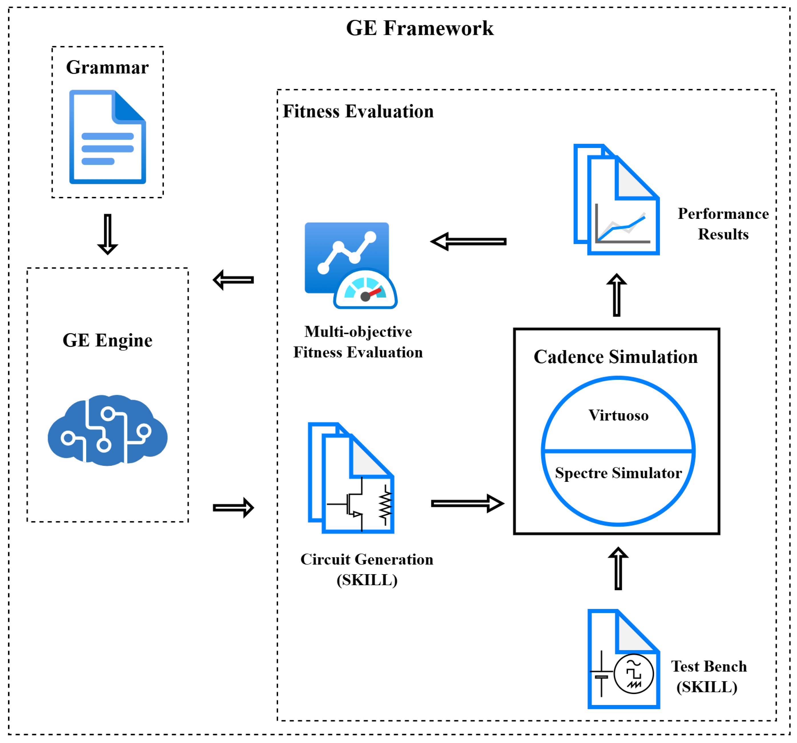
Following the standard GE workflow, each candidate solution begins as a binary genotype composed of codons. These codons are decoded using the user-defined AG to produce a syntactically valid SKILL program representing a complete circuit. The generated SKILL code is automatically instantiated as a schematic in Cadence Virtuoso, where components are connected according to the evolved topology (and device sizing in the case of analogue circuits). A custom testbench is then used to simulate the circuit using the Spectre simulator. Simulation outputs, including waveforms and key performance metrics, are extracted and evaluated, and the results are used to compute the fitness of each candidate. We employ separate grammars and fitness functions for digital and analogue circuits to reflect their differing behavioural requirements.
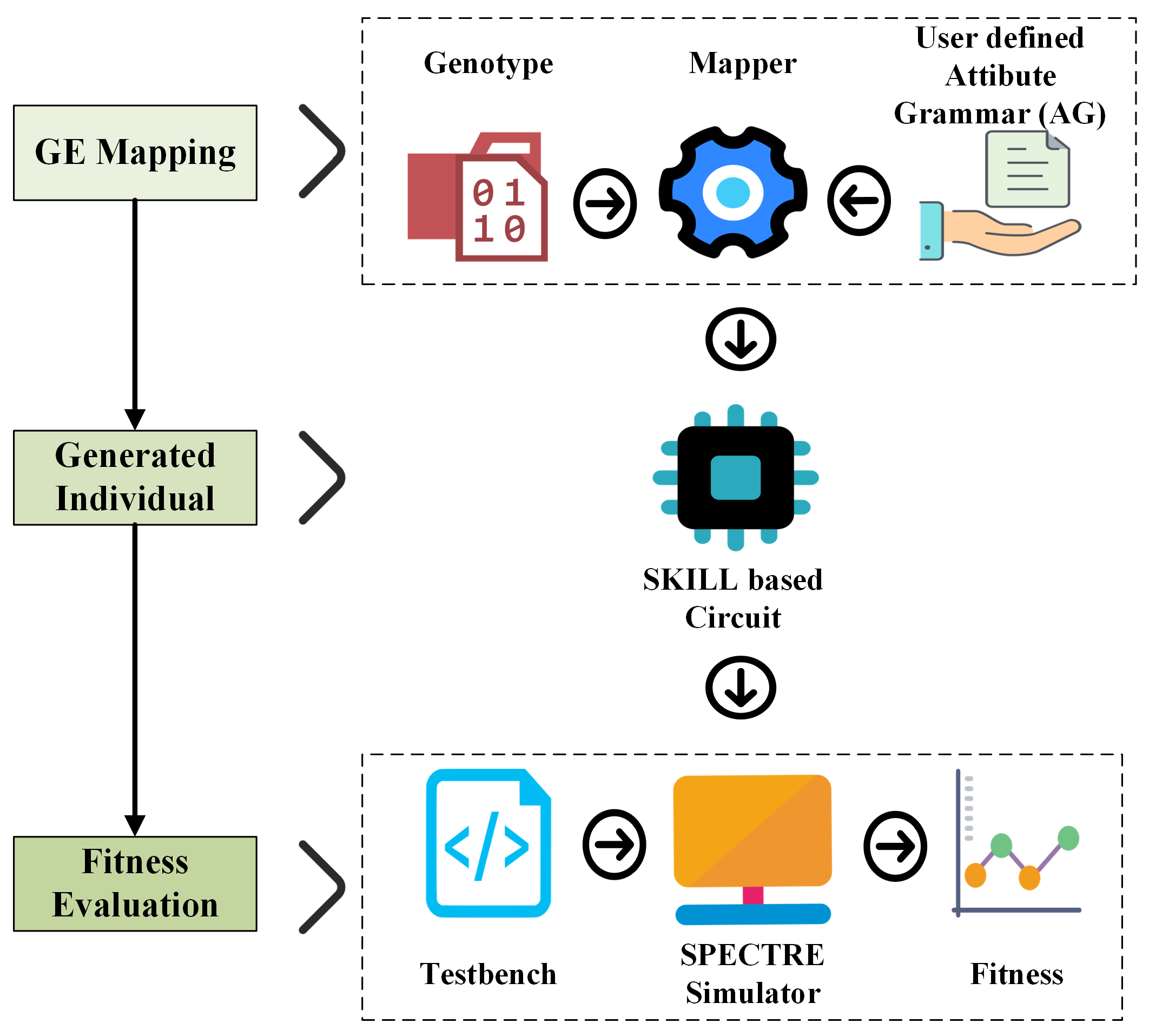
Figure 2 illustrates the overall process of automated transistor-level circuit design, from genotype decoding and SKILL-based schematic generation to simulation and fitness evaluation. Figure 3 shows the process flow of the framework, focusing on the GE mapping, generated circuits, and fitness evaluation.

4.1. Digital Circuit Grammar

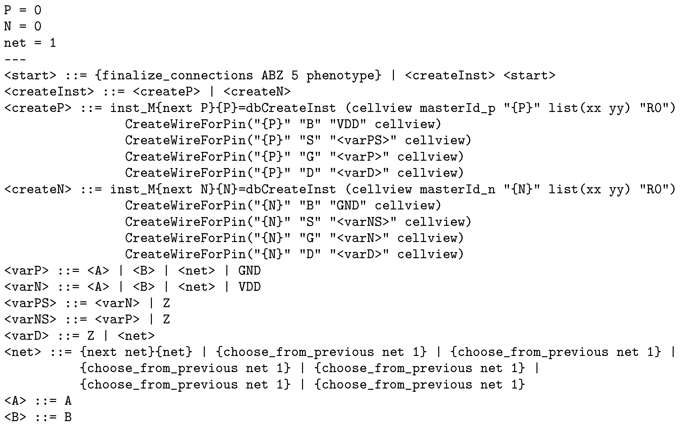
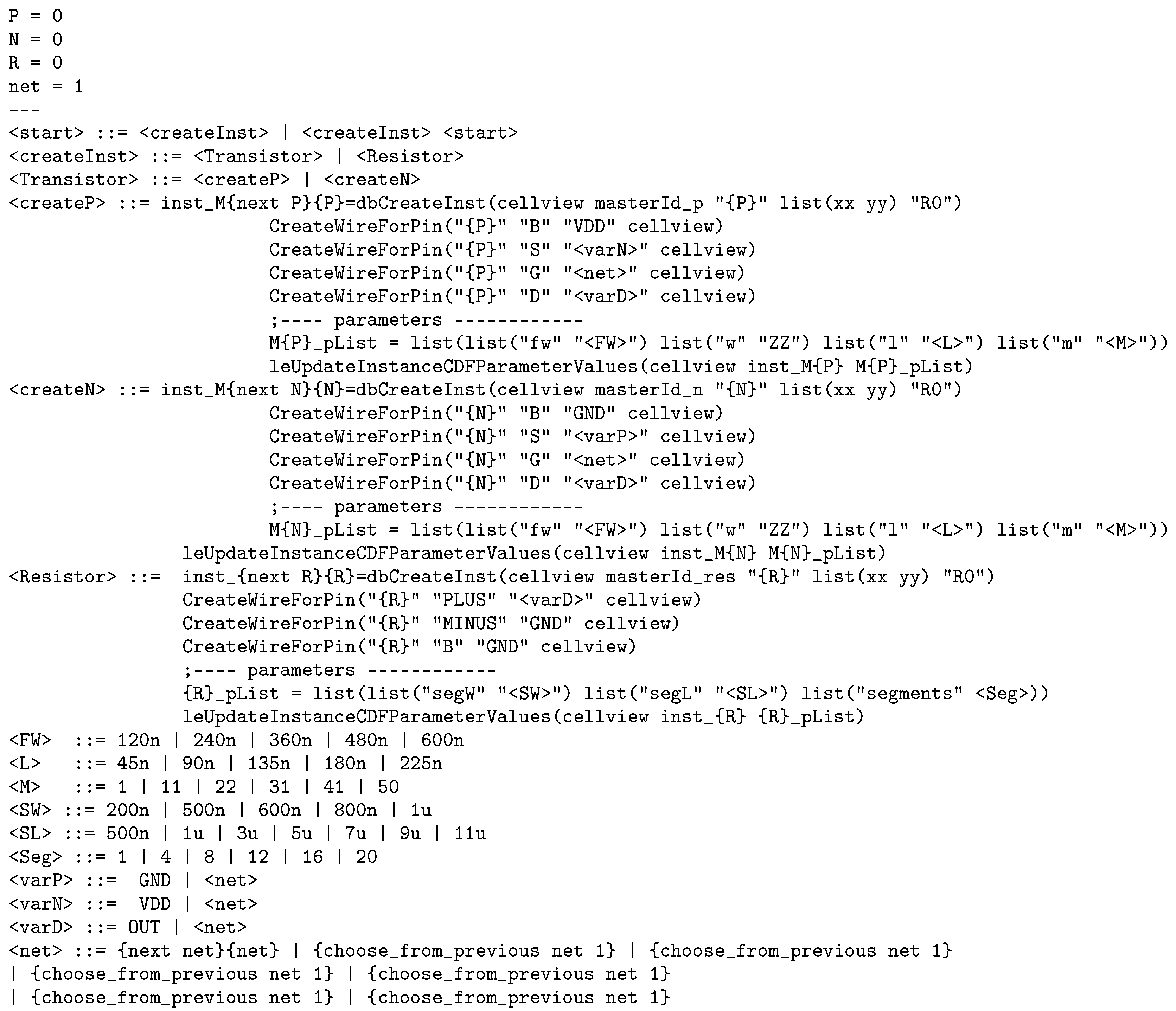
The digital grammar, see Figure 4, defines how to construct two-input, single-output circuits at the transistor level. It integrates Attribute Functions (AFs) directly into the production rules, ensuring that each transistor instance is named consistently, connected to valid nets, and wired without duplication or floating terminals. In practice, the grammar controls not only the syntactic form of SKILL code but also its semantic correctness.
The main components of the grammar are as follows:
  • Dynamic variable initialisation: Variables that are updated dynamically are initialised using the equality operator (=) to ensure consistent naming and reuse.
  • Core BNF components:
    (a)
    Start symbol: The entry point of the grammar, typically the leftmost non-terminal (e.g., <start>).
    (b)
    Production rules: Define how non-terminal symbols are expanded into terminals and other non-terminals. For example, <createInst> ::= <createP>|<createN>.
    (c)
    Terminals: Leaf symbols that appear in the final program, such as A, B, GND, VDD, and Z.
    (d)
    Non-terminals: Intermediate symbols used to structure the grammar (e.g., <createInst>).
  • AFs: Conceptually similar to semantic functions, these functions guide both initialisation and dynamic phenotype construction. They include the following:
    (a)
    Phenotype access functions: Ensure correct finalisation and integration of generated instances (e.g., {finalize_connections}), typically consuming multiple codons.
    (b)
    Attribute variables: Track state information such as transistor indices or net counts without consuming codons (e.g., {Next}).
    (c)
    Codon-consuming AFs: Functions like {choose_from_previous} allow reuse of previously defined nodes or nets, adding flexibility while consuming codons.
    (d)
    Substitution AFs: Inline substitution of dynamic variable values at specific points in the phenotype (e.g., {P}).

4.2. Genotype-to-Phenotype Decoding Example

To illustrate the mapping process, we present a step-by-step decoding of a 2-input conventional NAND gate. Consider the candidate chromosome
61, 20, 12, 23, 16, 22, 49, 7, 26, 31, 21, 171, 31, 57, 99, 110, 34, 76, 120, 156, 188, 220, 10, 15, 41,
40, 47, 125, 110, 74, 5
The decoding, using the grammar in Figure 4, proceeds as follows:
Step 1.
Mapping begins with <start>.
Step 2.
The first codon is picked, and a Modulo (MOD) operation is performed with 2, since there are two options in this production rule. Therefore, we calculate 61% 2, which is one. This chooses the <createInst> <start> rule. Note that execution proceeds from left to right.
Step 3.
20% 2; choose <createP> to create a PMOS transistor.
Step 4.
One attribute variable AF and six substitution AFs dynamically assign values to P. {next P} updates the index (e.g., P0 to P1), and {P} substitutes the updated index. No codons are consumed. Then, non-terminals <varPS><varP>, and <varD> are executed one by one.
Step 5.
12% 2 = 0; choose <varN>.
Step 6.
23% 4 = 3; choose terminal VDD.
Step 7.
16% 4 = 0; choose <A>, which yields A.
Step 8.
22% 2 = 0; choose terminal Z.
Step 9.
Execution returns to <start>. 49% 2 = 1; choose <createInst> <start>.
Step 10.
7% 2 = 1; choose <createN> to create an NMOS transistor.
Step 11.
Similarly to Step 4, variable N is dynamically assigned using attribute and substitution AFs.
Step 12.
26% 2 = 0; choose <varP>.
Step 13.
31% 4 = 3; choose terminal GND.
Step 14.
21% 4 = 1; choose <B>, which yields B.
Step 15.
171% 2 = 1; choose non-terminal <net>.
Step 16.
31% 7 = 3; choose {choose_from_previous}, which connects to net1, as net is initialised as 1.
Steps 17–22.
These steps repeat the logic from Steps 9 to 16, using codons 57, 99, 110, 34, 76, 120, and 156 to create an NMOS transistor connected to net1A, and Z.
Step 23.
<start> is executed again. Then 188% 2 = 0; choose {finalize_connection}.
Step 24.
{finalize_connection} consumes five codons (220, 10, 15, 41, and 40) and creates a PMOS transistor with Source, Gate, and Drain connected to VDD, B, and Z.
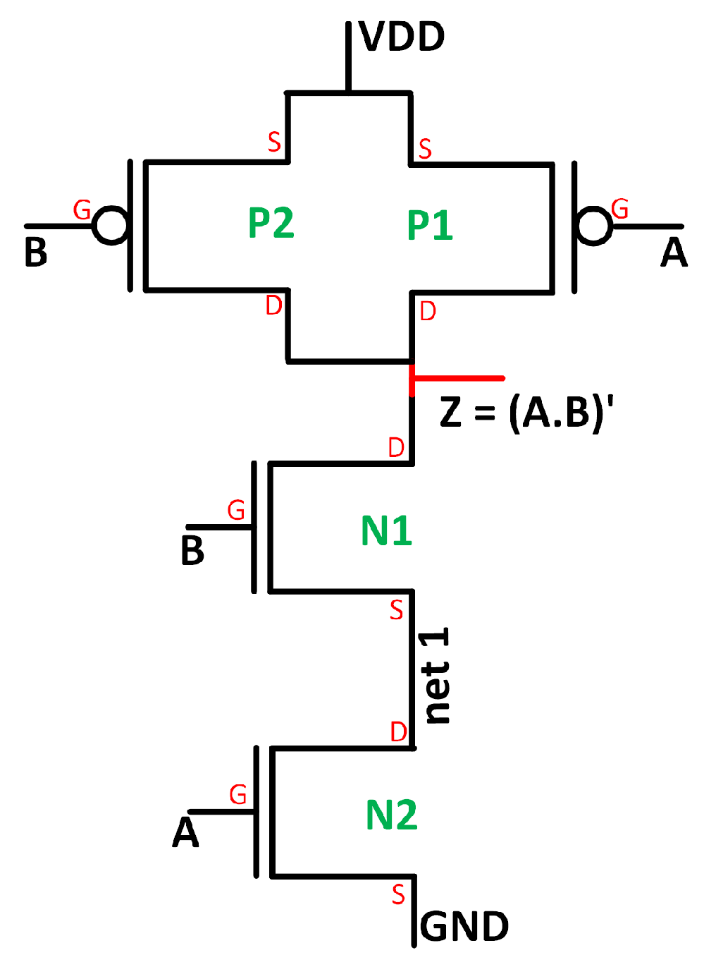
The remaining codons (47, 125, 110, 74, and 5) are unused. The resulting evolved NAND gate circuit is shown in Figure 5.

4.3. Analogue Circuit Grammar

Unlike digital designs, analogue circuits typically require passive components and careful device sizing. To capture this, the analogue grammar (Figure 6) extends the digital case by including PMOS/NMOS transistors as well as resistors. In addition to selecting topologies, the grammar evolves parameters such as transistor width, length, and multiplicity, as well as resistor segment width, length, and count. All previously discussed Attribute Functions (AFs) are used, except the phenotype access AF. These attributes ensure that parameter values are assigned consistently during phenotype construction, allowing both structure and sizing to be optimised simultaneously.
The analogue grammar can specify both topology and device sizing with fine granularity. For instance, a production choice may create a PMOS/NMOS transistor with a width selected from {120 nm, 240 nm, 360 nm, 480 nm, 600 nm}, a length from {45 nm, 90 nm, 135 nm, 180 nm, 225 nm}, and a multiplicity factor from {1, 11, 22, 31, 41, 50}. Similarly, a resistor may be generated with segment width (e.g., 200 nm–1 μm), segment length (e.g., 500 nm–11 μm), and a number of segments in series (e.g., 1–20). Attribute functions enforce these parameter assignments consistently during decoding. This level of control allows the evolutionary process to explore not only different circuit topologies but also fine-grained variations in device geometry and sizing.
Together, these expansions illustrate how the grammar can define both circuit topology and device sizing, ensuring that any generated design is not only syntactically valid SKILL code but also electrically plausible. Attribute functions guarantee consistent net reuse, parameter assignment, and connectivity, preventing illegal or floating designs.

4.4. Fitness Function

We adopt a multi-objective optimisation strategy for both digital and analogue circuits, reflecting their complex design requirements and dependence on multiple performance parameters. For digital circuits, the key objectives are correctness, area (in terms of transistor count), and power consumption. For analogue circuits, such as temperature sensors, additional objectives, including sensitivity and Integral Nonlinearity (INL), must also be considered. Together, these objectives determine which candidate circuits are selected as the best-performing individuals.
The multi-objective fitness function for digital circuits is defined in Equation (1):
F i t D i g i t a l ( O ) = m i n ( O C i r c u i t E r r o r , O T r a n s C o u n t , O A v g P o w e r )
This is a minimisation function where the following hold.
  • The first objective, O C i r c u i t E r r o r , measures how accurately the output of the evolved circuit matches that of a reference “gold” circuit—a version designed using conventional logic (CMOS, TGL, and GDI). Essentially, it captures the circuit’s error by comparing its outputs bit by bit:
    O C i r c u i t E r r o r = i = 0 N 1 1 ( C i r c u i t O u t i G o l d O u t i ) N
    Here, N represents the total number of binary bits tested. The function 1(·) is an indicator that returns 1 whenever the evolved circuit’s output bit differs from the corresponding bit in the gold circuit’s output and 0 when they match.
  • The second objective, O T r a n s C o u n t , estimates the circuit’s area by simply counting how many transistors are used in the evolved design:
    O T r a n s C o u n t = N t r a n s i s t o r s
    Here, N t r a n s i s t o r s is the total number of transistors in the evolved circuit.
  • The third objective ( O A v g P o w e r ) estimates the evolved circuit’s total average power consumption, calculated as follows:
    O A v g P o w e r = 1 T 0 T V ( t ) · I ( t ) d t
    Here, V ( t ) and I ( t ) are the instantaneous voltage and current, respectively, and T is the total simulation time.
For the analogue case, the objectives differ: sensitivity should be maximised, while INL, static power, and area should be minimised. The analogue fitness function is therefore
F i t A n a l o g u e ( O ) = m a x ( O S e n s i t i v i t y ) , m i n ( O I N L , O S t a t i c P o w e r , O T o t a l A r e a )
where the following hold:
  • The first objective, O S e n s i t i v i t y , represents how much the sensor’s output (typically voltage or current) changes in response to a change in temperature. This is usually expressed as the output change per degree Celsius (e.g., mV/°C) and is given by
    O S e n s i t i v i t y = 1 N i = 1 N [ V ( t i ) V ( t i Δ t ) Δ t ]
    Here, t i is the temperature at step i, given by T m i n + i · Δ t ;   Δ t is the temperature step size; V ( t i ) is the measured voltage at temperature t i ; and N is the total number of steps, given by T m a x T m i n Δ t , where T m a x and T m i n are the maximum and minimum temperatures.
  • The second objective, O I N L , is the INL, which measures the deviation of the sensor’s actual output from an ideal linear response across the temperature range. It indicates how accurately the sensor maintains a straight-line relationship between temperature and output and is given by
    O I N L = m a x 1 i N | V ( t i ) ( α + β t i ) |
    Here, α is the intercept of the best-fit line and β is the slope of the best-fit line.
  • The third objective, O S t a t i c P o w e r , estimates the static power consumption of the temperature sensor:
    O S t a t i c P o w e r = V · I
    Here, V represents the supply voltage and I represents the direct current.
  • Finally, O T o t a l A r e a estimates the actual area in terms of the number of devices in the circuit and the number of parameters associated with each device:
    O T o t a l A r e a = i = 1 n d e v i c e s l = 1 n p a r a m e t e r s , i P a r a m e t e r i , l
    Here, n d e v i c e s is the number of devices in the design; n p a r a m e t e r s , i is the number of parameters of the device i; i is the device counter; and l is the parameters’ counter.

4.5. Experimental Setup, Tools, and Evolutionary Parameters

Experiments were performed using Cadence Virtuoso together with Grammatical Algorithms in Python for Evolution (GRAPE), a Python 3.x-based implementation of GE [45]. GRAPE generated candidate circuit designs, which were instantiated and evaluated in Virtuoso to compute their fitness scores.
The setup ran on a Dell OptiPlex 7010 (Dell Inc., Round Rock, TX, USA) with 64 GB Random Access Memory (RAM) and a 13th-generation Intel (Intel Corporation, Santa Clara, CA, USA) Core i5 processor (2.5–4.8 GHz), under Red Hat Enterprise Linux (RHEL) 8.10 (Red Hat, Inc., Raleigh, NC, USA). The main evolutionary hyperparameters are listed in Table 1. For NAND and NOR circuits, each evolutionary run required approximately 78 h, while the analogue temperature sensor took around 120 h. Further discussion of these parameters and their role in GE can be found in [12].
A population size of 800 is employed in the evolutionary runs, substantially smaller than in related work [46,47,48]. This is because it often relies on very large populations to compensate for unconstrained encodings, leading to high simulator failure rates. In contrast, our framework embeds structural validity and domain semantics directly into the genotype-to-phenotype mapping, enabling stable and efficient search with a population several orders of magnitude smaller than that of classical GP-based topology synthesis. As the effective search effort in evolutionary algorithms is determined by the total number of fitness evaluations (population size × number of generations), the number of generations was kept constant. In contrast, the population size was incrementally increased during preliminary experiments. Convergence speed, fitness stability, and solution quality improved steadily up to a population size of 800, beyond which no statistically significant gains were observed.

5. Results and Evaluation

As outlined in Section 4, this study explores the evolution of two fundamental digital circuits, NAND and NOR, as well as an analogue temperature sensor. The digital circuits focused primarily on topology selection, while the analogue circuit required both appropriate topology selection and accurate device sizing. For the temperature sensor, the evolutionary process also involved the sizing of passive components, such as resistors, in addition to transistors. In contrast, the digital circuits were evolved exclusively using transistors.

5.1. Evolution of NAND/NOR (Digital Circuit)

One of the key fitness criteria for the digital circuits was output signal correctness, quantified using the O C i r c u i t E r r o r metric. To evaluate circuit performance under different interpretation thresholds, two logic levels were considered: 90–10% and 70–30%. These thresholds define voltage bounds used to distinguish logical high and low signals. For example, with a 1 V supply, the 90–10% threshold treats any signal above 900 mV as logic ‘1’ and any signal below 100 mV as logic ‘0’. Values in between are classified as undefined and penalised accordingly.
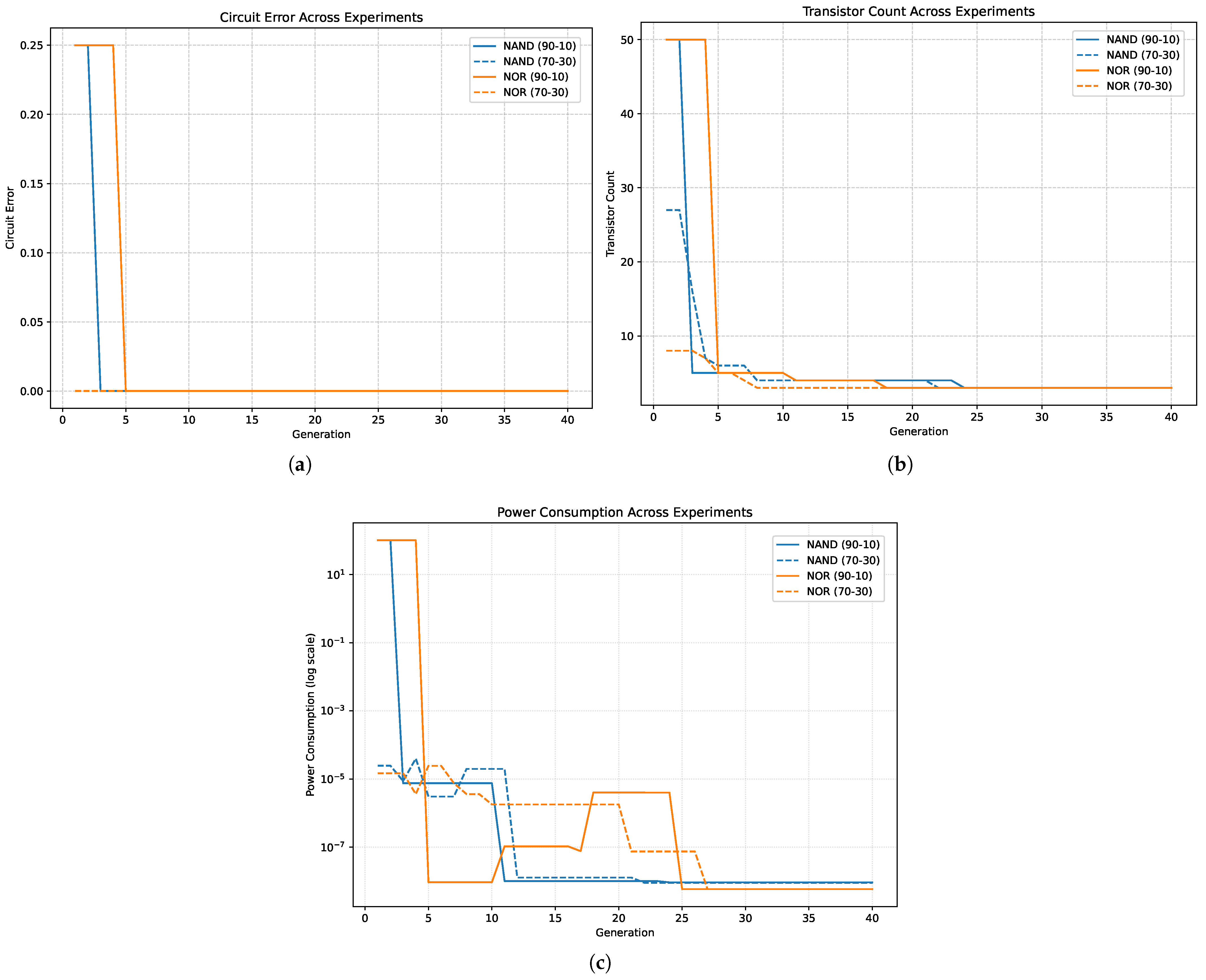
The evolutionary progression for both logic gates under these thresholds is shown in Figure 7, with results categorised by circuit error, transistor count, and power consumption. In Figure 7a, the error metric ranges from 0 (all output bits correct) to 1. An error score of 0.25, for instance, implies one incorrect bit out of four (see Equation (2)). Any non-zero error results in a poor overall fitness score, regardless of hardware efficiency in terms of transistor count or power.
At the 70–30% threshold, evolution consistently converged to zero-error solutions earlier than under the 90–10% condition. This trend is evident in both the error metric and the progression of transistor count and power consumption, shown in Figure 7b,c. The best evolved circuits for each threshold, together with their simulated output waveforms, are shown in Figure 8 and Figure 9. These simulations were performed in Cadence Virtuoso with Generic Process Design Kit (GPDK) 45 nm technology, over 80 ns at a 1 V supply. Circuits evolved under the stricter 90–10% threshold exhibited more stable, glitch-free outputs compared to their 70–30% counterparts. This is likely because stricter selection pressure allows fitter individuals to dominate earlier, leading to more robust designs.
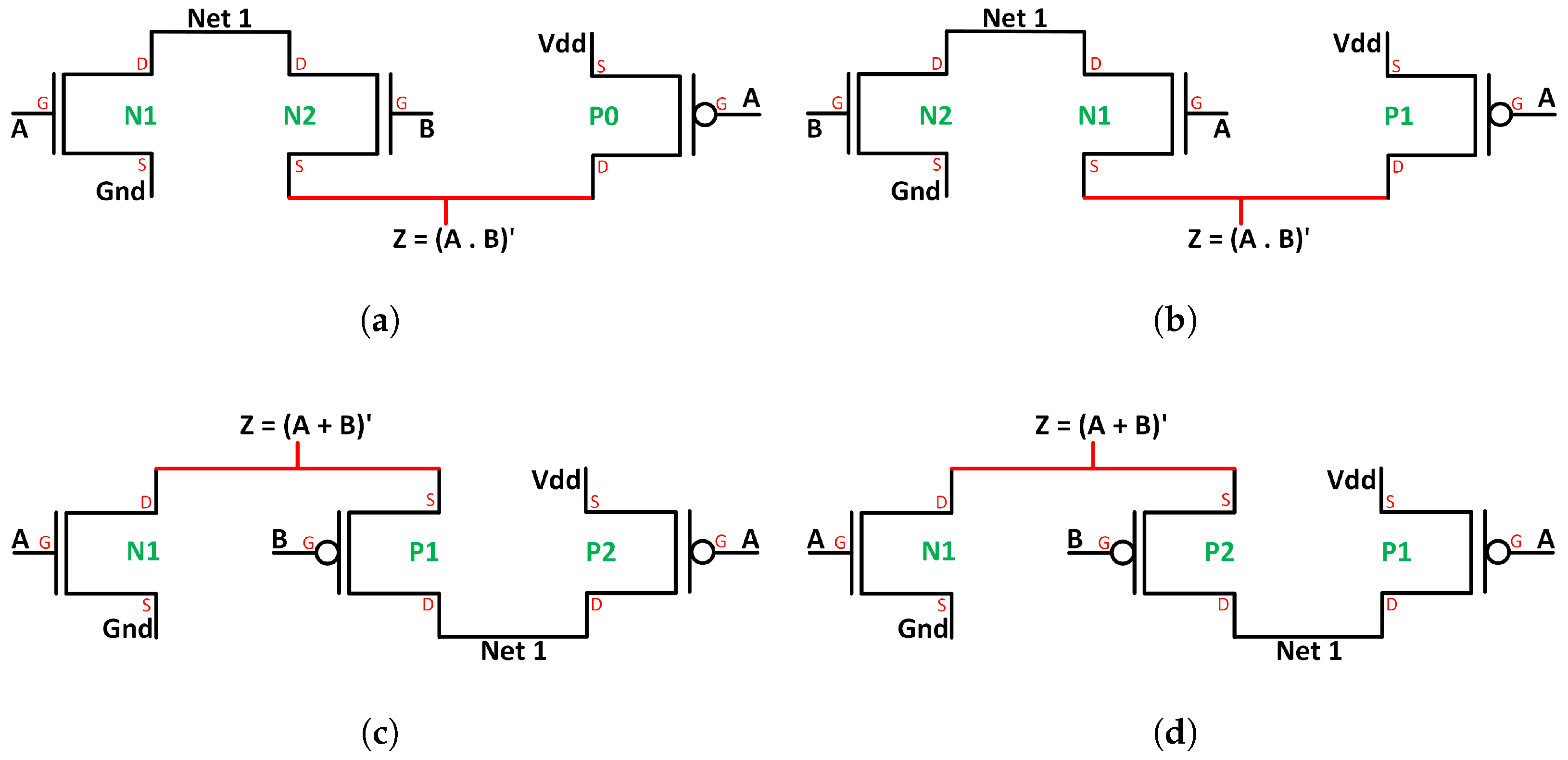
A particularly noteworthy outcome was the emergence of structural duality between the evolved NAND and NOR gates under the 90–10% threshold (Figure 8a,c). These circuits were not only logically complementary but also physically mirrored in their transistor configurations. According to the principle of duality in Boolean algebra, interchanging AND with OR and swapping logic ‘0’ with logic ‘1’ yields a dual function. Here, this corresponds to swapping PMOS with NMOS transistors and exchanging V D D and G N D connections. Remarkably, this duality emerged even though the NAND and NOR circuits were evolved in completely independent runs, with no shared constraints. The evolutionary algorithm had no built-in knowledge of this relationship yet converged independently to a meaningful structural result. By contrast, circuits evolved under the 70–30% threshold did not exhibit such symmetry, suggesting a less constrained, more exploratory search.
Another important observation is that the evolved NOR circuits under both thresholds (Figure 8c,d) are identical. Despite evolving independently, the process converged on the same design. This is likely because, even with the relaxed 70–30% threshold, no further optimisation was possible in terms of correctness, transistor count, or power. In contrast, the NAND designs differ across thresholds (Figure 8a,b).
These results highlight GE’s capacity to uncover elegant, low-level circuit solutions without explicit guidance. Its ability to explore diverse design spaces and converge on underlying structural principles demonstrates its promise as a hardware design automation tool, especially where prior design knowledge is limited.
The performance comparison between evolved gates and conventional logic styles (gold) is shown in Table 2 and Table 3. At both thresholds, all evolved designs achieved 100% functional correctness. They also outperformed conventional counterparts across most parameters, except propagation delay in the GDI-based designs. Given the trade-off between power and delay, the Power–Delay Product (PDP) was also evaluated, and in this metric, the evolved circuits again showed a clear advantage.

5.2. Evolution of Temperature Sensor (Analogue Circuit)

The evolution of a temperature sensor differs from the digital case in several important ways. Unlike the evolved digital circuits, which consist solely of transistors, the temperature sensor designs also incorporate resistors. In addition to choosing the appropriate topology, both transistor and resistor sizing must be determined. For transistors, the grammar evolves width (W), length (L), and the multiplication factor applied to the width (m). For resistors, the parameters include segment width ( s e g W ), segment length ( s e g L ), and the number of segments connected in series or parallel ( s e g m e n t s ). As described in Section 4.4, the fitness function considers sensitivity, INL, area, and power consumption, with priority given to maximising sensitivity and minimising INL. If sensitivity and INL fail to meet the thresholds of the conventional Proportional to Absolute Temperature (PTAT) [49] or “gold” circuit, the individual is penalised and the remaining metrics (area and power) are disregarded.
This makes the temperature sensor design task more robust and dynamic than digital circuits, since it incorporates both active and passive devices with multiple sizing parameters. The resulting search space for GE is significantly larger, enabling exploration of a wide range of configurations to identify the best-fit designs.
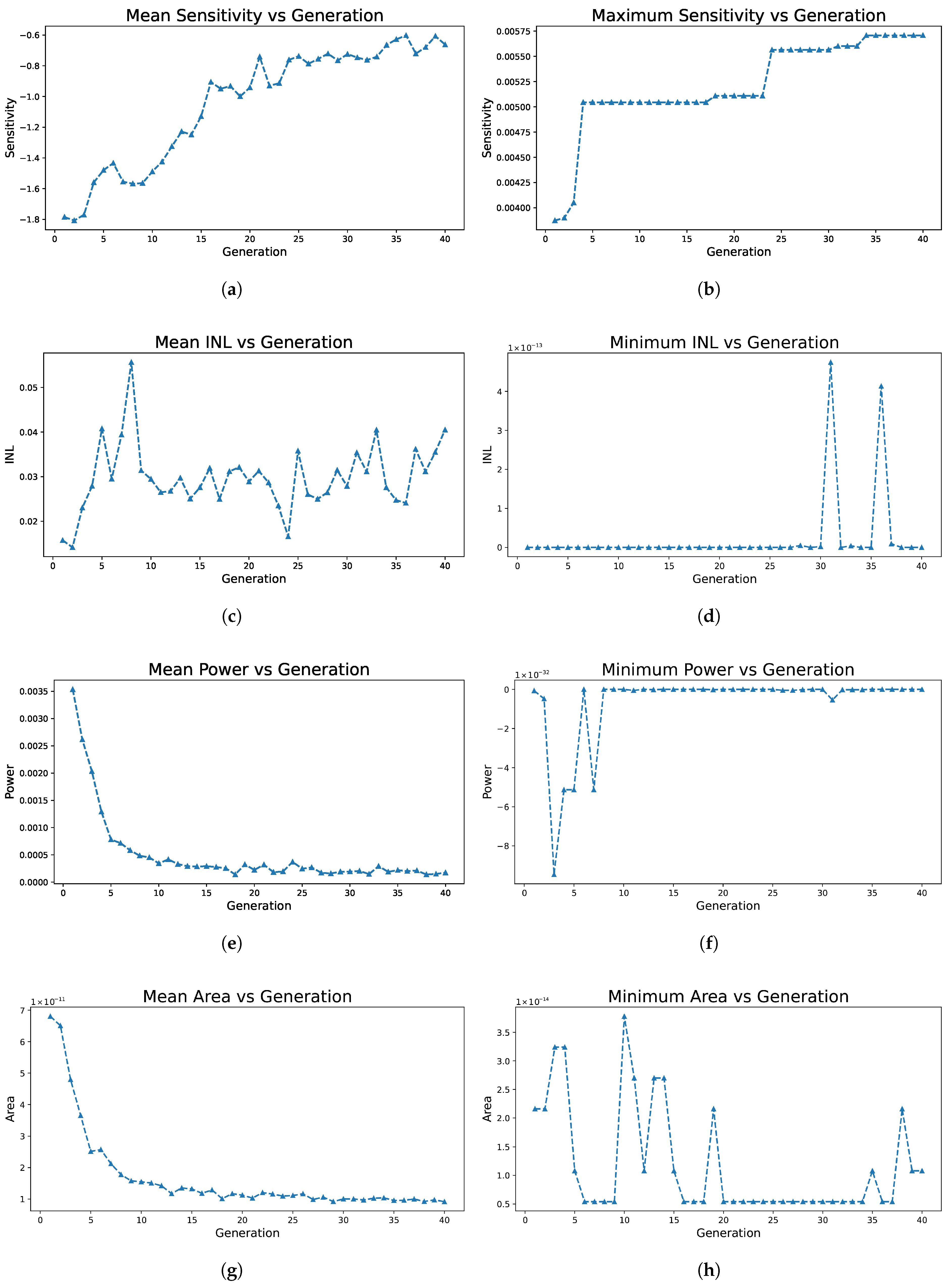
Figure 10 shows the evolution trends of the temperature sensor across fitness objectives. Figure 10a,b plot the mean and maximum sensitivity per generation, both showing a steady upward trend, highlighting the algorithm’s effectiveness in discovering higher-sensitivity designs. Figure 10c,d present the mean and minimum INL. The mean INL fluctuates before stabilising, while the minimum INL shows two pronounced spikes in later generations, reflecting intensified search for high-sensitivity configurations. Figure 10e,f track mean and minimum power consumption, which fall sharply early on before converging to low-power solutions. Finally, Figure 10g,h show the mean and minimum chip area, both decreasing rapidly before levelling off.
When calculating means, invalid individuals were excluded. Including them would have distorted the results, as averaging extremely high values (from invalid designs) with low values (from valid designs) would make all objectives appear artificially similar. Overall, the plots confirm that each objective evolves at a distinct rate and stability, reflecting intrinsic trade-offs between them.
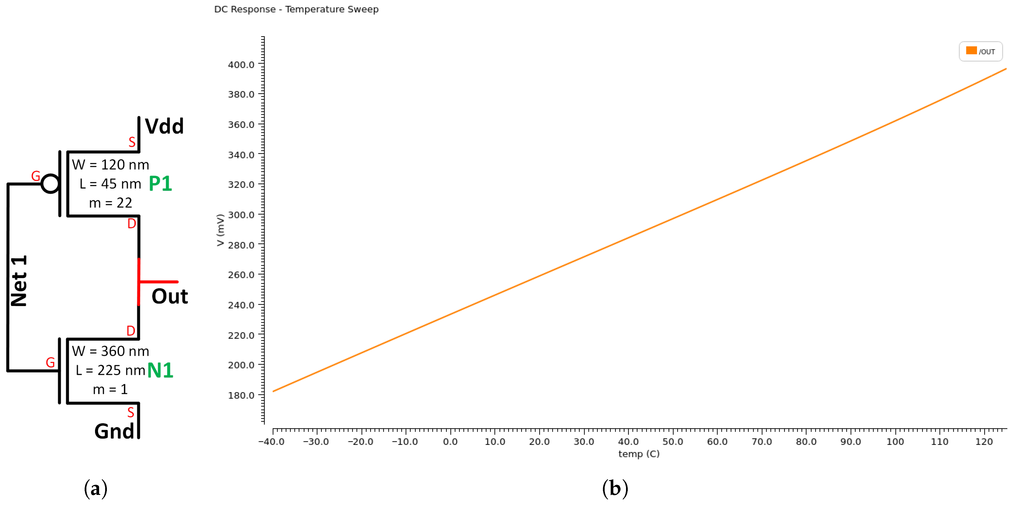
Figure 11 shows the best-fit evolved design and its voltage–temperature characteristic. The conventional PTAT (gold) [49] circuit requires at least three PMOS, two NMOS, and two resistors. In contrast, the evolved circuit utilises only two transistors and no resistors yet delivers superior performance. It achieves higher sensitivity and lower INL, area, and static power consumption, as summarised in Table 4.

6. Discussion

This study demonstrates that GE can effectively generate fully functional transistor-level circuit designs without direct human intervention. The evolution graphs and comparative performance tables clearly show GE’s capability to identify high-performing designs in a relatively short time. In both analogue and digital experiments, GE evolved syntactically valid and functionally correct circuits that outperformed their manually designed “gold” counterparts. In many cases, individuals with better performance emerged within the first 10 to 15 generations. The total time required to obtain the best-fit individual was primarily determined by the simulation-based fitness evaluation in the Cadence Spectre environment, rather than the GE process itself. Since GE must wait for each candidate’s fitness to be evaluated before moving to the next generation, simulation time remains the main bottleneck. If parallel simulation methods were available, the evolution process could be significantly faster. This answers the first research question we presented in Section 1 (RQ1).
Another important observation is that the runtime per evolutionary run did not vary significantly with circuit complexity. Using identical hyperparameters (Table 1), GE required approximately the same amount of time to evolve digital circuits and only slightly more time for the more complex analogue designs, such as the temperature sensor. This difference is not due to the number of inputs being handled, but rather the number of objective functions involved in the fitness evaluation. In the digital experiments, the fitness function focused on correctness, minimisation of transistor count (which does not require simulation), and average power. In contrast, the analogue experiments incorporated sensitivity and INL, along with static power consumption and area, all of which required simulation. As a result, the analogue designs demanded more simulation steps per individual in Cadence Spectre. This suggests that scalability, in terms of the number of variables or signals, would not significantly impact runtime, provided that the number of objective functions remains constant. This consistent performance across varying complexity levels highlights GE’s suitability for a broad range of circuit design tasks.
The importance of multi-objective optimisation is also evident (RQ2). When optimisation is driven by a single objective—such as correctness in digital circuits or sensitivity in analogue sensors—other critical parameters remain unoptimised. In contrast, the multi-objective fitness functions used here balanced correctness, transistor count, power, and delay for digital circuits, as well as sensitivity, INL, area, and static power for analogue circuits. This allowed GE to discover solutions that were not only correct but also efficient, compact, and power-conscious. Multi-objective optimisation, therefore, better reflects the trade-offs encountered in real-world circuit design.
Results across both domains indicate that the automated system can consistently produce competitive and often superior designs compared to manual solutions (RQ3). In the digital experiments, both NAND and NOR gates converged to correct designs at 70–30% and 90–10% thresholds within a single run. In the analogue case, the evolved temperature sensor achieved higher sensitivity and lower INL, area, and static power than the PTAT (gold) design, despite requiring fewer devices. The grammar’s flexibility to vary both topology and device sizing proved highly effective in enabling these improvements.
Overall, the findings confirm that GE, when combined with robust multi-objective evaluation, is a scalable and powerful approach to automated circuit synthesis. It delivers consistent results across design complexities and technology nodes. By reducing reliance on manual intervention, it has the potential to shorten design cycles, lower costs, and make custom IC development more accessible, contributing toward the development of fully automated electronic design flows. Table 5 presents a comparison of the existing methods and the proposed method in terms of applications, key contributions, and limitations.

7. Conclusions

In this work, we set out to investigate whether GE can (i) automatically generate correct transistor-level analogue and digital circuits, (ii) operate efficiently across different objectives and circuit types, and (iii) reduce or eliminate the need for manual design intervention. The results presented in this paper demonstrate that all of these aims, defined in Section 1 and formalised in RQ1–RQ3, have been successfully achieved.
This work has shown that GE can automate the design of fully functional transistor-level circuits without human intervention. In both analogue and digital domains, GE consistently evolved valid and correct designs that matched or outperformed manually engineered “gold” counterparts, often within the first 10–15 generations. These results confirm RQ1 and RQ3: GE is capable of producing competitive, high-performing designs across circuit types without domain-specific expertise.
A key finding is that runtime was determined primarily by simulation in Cadence Spectre rather than by the evolutionary process itself. This makes simulation the main bottleneck, suggesting that parallel or accelerated simulation would substantially reduce runtime. Importantly, scalability was not strongly affected by circuit complexity: digital and analogue experiments required a similar runtime, with differences arising from the number of simulation-based objectives. This consistency supports GE’s applicability to a wide range of design tasks (RQ1).
The role of multi-objective optimisation (RQ2) was also clear. By balancing correctness, area, power, and delay in digital circuits and sensitivity, INL, area, and static power in analogue designs, GE produced solutions that were both functionally correct and resource-efficient. This reflects the real-world trade-offs of circuit design more faithfully than single-objective optimisation.

Author Contributions

Conceptualisation, R.S. and C.R.; methodology, R.S., M.K.N.S., D.K.S. and C.R.; software, R.S., D.K.S. and M.K.N.S.; validation, R.S. and D.K.S.; formal analysis, R.S.; investigation, R.S. and C.R.; resources, R.S. and D.K.S.; writing—original draft preparation, R.S.; writing—review and editing, R.S., M.K.N.S., D.K.S. and C.R.; supervision, R.S. and C.R.; project administration, R.S. and C.R.; funding acquisition, C.R. All authors have read and agreed to the published version of the manuscript.

Funding

This publication has emanated from research conducted with the financial support of Taighde Éireann—Research Ireland under grant number 13/RC/2094_2.

Data Availability Statement

The original contributions presented in this study are included in the article. Further inquiries can be directed to the corresponding authors.

Acknowledgments

The authors acknowledge Lero, the Research Ireland Centre for Software, and the CSIS Department at the University of Limerick for providing a world-class laboratory environment.

Conflicts of Interest

The authors declare no conflicts of interest.

References

  1. Razavi, B. Design of Analog CMOS Integrated Circuits; McGraw-Hill Education: Columbus, OH, USA, 2000. [Google Scholar]
  2. Rabaey, J.M.; Chandrakasan, A.; Nikolic, B. Digital Integrated Circuits: A Design Perspective, 2nd ed.; Prentice Hall: Hoboken, NJ, USA, 2003. [Google Scholar]
  3. Nassif, S.R. Modeling and analysis of manufacturing variations. In Proceedings of the Custom Integrated Circuits Conference (CICC), San Diego, CA, USA, 9–9 May 2001; IEEE: Piscataway, NJ, USA, 2000; pp. 223–228. [Google Scholar]
  4. Borkar, S. Design challenges of technology scaling. IEEE Micro 1999, 19, 23–29. [Google Scholar] [CrossRef]
  5. Semiconductor, F. CMOS, the Ideal Logic Family. Application Note 77. 1983. Available online: https://shrubbery.net/~heas/willem/PDF/NSC/AN/AN-77.pdf (accessed on 13 November 2025).
  6. Al-Assadi, W.; Jayasumana, A.P.; Malaiya, Y.K. Pass-transistor logic design. Int. J. Electron. Theor. Exp. 1991, 70, 739–749. [Google Scholar] [CrossRef]
  7. Morgenshtein, A.; Fish, A.; Wagner, I.A. Gate-diffusion input (GDI): A power-efficient method for digital combinatorial circuits. IEEE Trans. Very Large Scale Integr. (VLSI) Syst. 2003, 10, 566–581. [Google Scholar] [CrossRef]
  8. Milovanovic, D.P.; Litovski, V.B. Fault models of CMOS transmission gate. Int. J. Electron. 1991, 71, 675–683. [Google Scholar] [CrossRef]
  9. Harel, D.; Kozen, D.; Tiuryn, J. Dynamic logic. ACM SIGACT News 2001, 32, 66–69. [Google Scholar] [CrossRef]
  10. Johns, D.A.; Martin, K. Analog Integrated Circuit Design; Wiley: Hoboken, NJ, USA, 1997. [Google Scholar]
  11. Laker, K.R.; Sansen, W.M.C. Design of Analog Integrated Circuits and Systems; McGraw-Hill: Columbus, OH, USA, 1994. [Google Scholar]
  12. Ryan, C.; Collins, J.; Neill, M.O. Grammatical evolution: Evolving programs for an arbitrary language. In Proceedings of the European Conference on Genetic Programming, Paris, France, 14–15 April 1998; Banzhaf, W., Poli, R., Schoenauer, M., Fogarty, T.C., Eds.; Springer: Berlin/Heidelberg, Germany, 1998; pp. 83–96. [Google Scholar]
  13. Bäck, T.; Fogel, D.B.; Michalewicz, Z. Handbook of Evolutionary Computation; IOP Publishing Ltd.: Bristol, UK; Oxford University Press: Oxford, UK, 1997. [Google Scholar]
  14. Holland, J.H. Genetic algorithms. Sci. Am. 1992, 267, 66–72. [Google Scholar] [CrossRef]
  15. Koza, J.R. Genetic Programming: On the Programming of Computers by Means of Natural Selection; MIT Press: Cambridge, MA, USA, 1992. [Google Scholar]
  16. Ryan, C.; Tetteh, M.; McEllin, J.; Mota-Dias, D.; Conway, R.; Naredo, E. ADDC: Automatic design of digital circuit. In Genetic Algorithms; IntechOpen: London, UK, 2022. [Google Scholar]
  17. Tetteh, M.; Dias, D.M.; Ryan, C. Grammatical evolution of complex digital circuits in SystemVerilog. SN Comput. Sci. 2022, 3, 188. [Google Scholar] [CrossRef]
  18. Majeed, B.; McEllin, J.; Sarma, R.; Youssef, A.; Dias, D.; Ryan, C. Grammatical Evolution of Synthesizable Finite State Machine-Based Behavioural Level Hardware Description Language Codes. In Proceedings of the 16th International Joint Conference on Computational Intelligence—ECTA. INSTICC, Porto, Portugal, 20–22 November 2024; SciTePress: Setúbal, Portugal, 2024; pp. 222–233. [Google Scholar] [CrossRef]
  19. Deb, K.; Pratap, A.; Agarwal, S.; Meyarivan, T. A fast and elitist multiobjective genetic algorithm: NSGA-II. IEEE Trans. Evol. Comput. 2002, 6, 182–197. [Google Scholar] [CrossRef]
  20. Blickle, T. Tournament selection. Evol. Comput. 2000, 1, 181–186. [Google Scholar]
  21. Helmuth, T.; Spector, L.; Matheson, J. Solving Uncompromising Problems with Lexicase Selection. IEEE Trans. Evol. Comput. 2015, 19, 630–643. [Google Scholar] [CrossRef]
  22. de la Cruz Echeandía, M.; de la Puente, A.O.; Alfonseca, M. Attribute grammar evolution. In Proceedings of the International Work-Conference on the Interplay Between Natural and Artificial Computation, Las Palmas, Spain, 15–18 June 2005; Springer: Berlin/Heidelberg, Germany, 2005; pp. 182–191. [Google Scholar]
  23. Karim, M.R.; Ryan, C. On improving grammatical evolution performance in symbolic regression with attribute grammar. In Proceedings of the Companion Publication of the 2014 Annual Conference on Genetic and Evolutionary Computation, Vancouver, BC, Canada, 12–16 July 2014; pp. 139–140. [Google Scholar]
  24. Girardi, A.; De-Oliveira, T.; Ghissoni, S.; Aguirre, P.C.; Compassi-Severo, L. A comprehensive review on automation-based sizing techniques for analog IC design. J. Integr. Circuits Syst. 2022, 17, 1–14. [Google Scholar] [CrossRef]
  25. Zebulum, R.; Pacheco, M.; Vellasco, M. Comparison of different evolutionary methodologies applied to electronic filter design. In Proceedings of the 1998 IEEE International Conference on Evolutionary Computation Proceedings. IEEE World Congress on Computational Intelligence (Cat. No.98TH8360), Anchorage, Alaska, 4–9 May 1998; pp. 434–439. [Google Scholar] [CrossRef]
  26. Koza, J.R. Genetic Programming III: Darwinian Invention and Problem Solving; Morgan Kaufmann: Burlington, MA, USA, 1999; Volume 3. [Google Scholar]
  27. Tlelo-Cuautle, E.; Duarte-Villaseáor, M.A. Evolutionary electronics: Automatic synthesis of analog circuits by GAs. In Success in Evolutionary Computation; Springer: Berlin/Heidelberg, Germany, 2008; pp. 165–187. [Google Scholar]
  28. Salgado, G.R.; Reyes-Garcia, C.A. Applications of evolutionary algorithms in the design automation of analog integrated circuits. J. Appl. Sci. 2010, 10, 1859–1872. [Google Scholar] [CrossRef]
  29. Kim, K.J.; Cho, S.B. Automated synthesis of multiple analog circuits using evolutionary computation for redundancy-based fault-tolerance. Appl. Soft Comput. 2012, 12, 1309–1321. [Google Scholar] [CrossRef]
  30. Mühlenbein, H.; Zinchenko, L.; Kureichik, V.; Mahnig, T. Effective mutation rate for probabilistic evolutionary design of analogue electrical circuits. Appl. Soft Comput. 2007, 7, 1012–1018. [Google Scholar] [CrossRef]
  31. Yao, X.; Higuchi, T. Promises and challenges of evolvable hardware. IEEE Trans. Syst. Man, Cybern. Part C (Appl. Rev.) 1999, 29, 87–97. [Google Scholar] [CrossRef]
  32. McConaghy, T.; Gielen, G. Genetic programming in industrial analog CAD: Applications and challenges. In Genetic Programming Theory and Practice III; Springer: Boston, MA, USA, 2006; pp. 291–306. [Google Scholar]
  33. O’Neill, M.; Brabazon, A. Recent patents on genetic programming. Recent Patents Comput. Sci. 2009, 2, 43–49. [Google Scholar]
  34. McConaghy, T.; Palmers, P.; Steyaert, M.; Gielen, G.G. Variation-aware structural synthesis of analog circuits via hierarchical building blocks and structural homotopy. IEEE Trans. Comput.-Aided Des. Integr. Circuits Syst. 2009, 28, 1281–1294. [Google Scholar] [CrossRef]
  35. McConaghy, T.; Eeckelaert, T.; Gielen, G. CAFFEINE: Template-free symbolic model generation of analog circuits via canonical form functions and genetic programming. In Proceedings of the Design, Automation and Test in Europe, Munich, Germany, 7–11 March 2005; IEEE: Piscataway, NJ, USA, 2005; pp. 1082–1087. [Google Scholar]
  36. Kunaver, M. Grammatical evolution-based analog circuit synthesis. Inf. MIDEM 2019, 49, 229–240. [Google Scholar]
  37. Castejón, F.; Carmona, E.J. Automatic design of analog electronic circuits using grammatical evolution. Appl. Soft Comput. 2018, 62, 1003–1018. [Google Scholar] [CrossRef]
  38. Žaloudek, L.; Sekanina, L. Transistor-level evolution of digital circuits using a special circuit simulator. In Proceedings of the International Conference on Evolvable Systems, Prague, Czech Republic, 21–24 September 2008; Springer: Berlin/Heidelberg, Germany, 2008; pp. 320–331. [Google Scholar]
  39. Campilho-Gomes, M.; Tavares, R.; Goes, J. Automatic flat-level circuit generation with genetic algorithms. In Proceedings of the Doctoral Conference on Computing, Electrical and Industrial Systems, Costa de Caparica, Portugal, 1–3 July 2020; Springer: Berlin/Heidelberg, Germany, 2020; pp. 101–108. [Google Scholar]
  40. Bennett, F.H., III; Koza, J.R.; Keane, M.A.; Yu, J.; Mydlowec, W.; Stiffelman, O. Evolution by Means of Genetic Programming of Analog Circuits that Perform Digital Functions. In Proceedings of the GECCO, Orlando, FL, USA, 13–17 July 1999; pp. 1477–1483. [Google Scholar]
  41. Settaluri, K.; Haj-Ali, A.; Huang, Q.; Hakhamaneshi, K.; Nikolic, B. Autockt: Deep reinforcement learning of analog circuit designs. In Proceedings of the 2020 Design, Automation & Test in Europe Conference & Exhibition (DATE), Grenoble, France, 9–13 March 2020; IEEE: Piscataway, NJ, USA, 2020; pp. 490–495. [Google Scholar]
  42. Wang, H.; Wang, K.; Yang, J.; Shen, L.; Sun, N.; Lee, H.S.; Han, S. GCN-RL circuit designer: Transferable transistor sizing with graph neural networks and reinforcement learning. In Proceedings of the 2020 57th ACM/IEEE Design Automation Conference (DAC), San Francisco, CA, USA, 20–24 July 2020; IEEE: Piscataway, NJ, USA, 2020; pp. 1–6. [Google Scholar]
  43. Petrus, E.S. SKILL: A Lisp based extension language. ACM SIGPLAN Lisp Pointers 1993, 6, 71–79. [Google Scholar] [CrossRef]
  44. Alloatti, L.; Wade, M.; Stojanovic, V.; Popovic, M.; Ram, R.J. Photonics design tool for advanced CMOS nodes. IET Optoelectron. 2015, 9, 163–167. [Google Scholar] [CrossRef]
  45. de Lima, A.; Carvalho, S.; Dias, D.M.; Naredo, E.; Sullivan, J.P.; Ryan, C. GRAPE: Grammatical Algorithms in Python for Evolution. Signals 2022, 3, 642–663. [Google Scholar] [CrossRef]
  46. Koza, J.R.; Bennett, F.H., III; Andre, D.; Keane, M.A. Automated design of both the topology and sizing of analog electrical circuits using genetic programming. In Artificial Intelligence in Design’96; Springer: Dordrecht, The Netherlands, 1996; pp. 151–170. [Google Scholar]
  47. Noren, K.V.; Ross, J.E. Analog circuit design using genetic algorithms. In Proceedings of the Second Online Symposium for Electronics Engineers, Denver, CO, USA, 7–9 May 2001. [Google Scholar]
  48. Karci, H.; Tohumoğlu, G.; Nacaroğlu, A. Speciation-based genetic algorithm in analog circuit design. Turk. J. Electr. Eng. Comput. Sci. 2016, 24, 1022–1033. [Google Scholar] [CrossRef]
  49. Malits, M.; Brouk, I.; Nemirovsky, Y. Study of CMOS-SOI Integrated Temperature Sensing Circuits for On-Chip Temperature Monitoring. Sensors 2018, 18, 1629. [Google Scholar] [CrossRef]
Figure 1. Steps involved in analogue (transistor-level) circuit design [24].
Symmetry 17 02169 g001
Figure 2. Mapping, SKILL-based automated transistor-level circuit generation, and subsequent fitness evaluation within the proposed methodology.
Symmetry 17 02169 g002
Figure 3. Process flow consisting of the GE mapping, generated circuits, and fitness evaluation.
Symmetry 17 02169 g003
Figure 4. The AG for two-input (A and B), single-output (Z) digital circuit defines the complete structure of the SKILL code, including the evolution of transistor types (P-channel MOSFET (PMOS) or N-channel MOSFET (NMOS)) and signals (<net>). It also handles the assignment of net names and instance names, with the flexibility to create new ones or reuse existing ones. Note that ( xx   yy ) represents the coordinates of each PMOS/NMOS instance, which are assigned random values in the range [ 0 , 100 ] prior to fitness evaluation.
Symmetry 17 02169 g004
Figure 5. A conventional 2-input NAND gate evolved using GE. S, D, and G represent the source, drain and gate terminals of the transistors respectively. P1 and P2 are instances of PMOS transistors, and N1 and N2 are instances of NMOS transistors. A and B denote the inputs, and Z denotes the output. The output node is highlighted in red.
Symmetry 17 02169 g005
Figure 6. The specialised AG for a temperature sensor circuit not only defines the topology but also allows the sizing of transistors and the resistor.
Symmetry 17 02169 g006
Figure 7. Objective-wise evolution across generations for a single run. (a) Output correctness vs. generation. (b) Transistor count vs. generation. (c) Power consumption vs. generation.
Symmetry 17 02169 g007
Figure 8. Evolved circuits at 70–30% and 90–10% logic thresholds. The label NC denotes “no connection” or “open circuit”. (a) NAND at 90–10%. (b) NAND at 70–30%. (c) NOR at 90–10%. (d) NOR at 70–30%. S, D, and G represent the source, drain and gate terminals of the transistors respectively. P0, P1, and P2 are instances of PMOS transistors, and N1 and N2 are instances of NMOS transistors. A and B denote the inputs, and Z denotes the output. The output nodes in each of the four circuits are highlighted in red.
Symmetry 17 02169 g008
Figure 9. Output waveforms of the evolved NAND and NOR gates at the 90–10% and 70–30% thresholds.
Symmetry 17 02169 g009
Figure 10. Evolution trends of the temperature sensor across the fitness objectives for a single, representative run. (a,b) Show the mean and maximum sensitivity per generation. (c,d) Present the mean and minimum INL per generation. (e,f) Track the mean and minimum power consumption per generation. Finally, (g,h) show the mean and minimum chip area.
Symmetry 17 02169 g010
Figure 11. Evolved temperature sensor (a) with topology selection and transistor sizing. Check the variation in the width (W), length (L), and the multiplication factor applied to the width (m) in the transistors. The width and length are expressed in nanometres (nm). S, D, and G represent the source, drain and gate terminals of the transistors respectively. P1 and N1 are the instances of PMOS and NMOS transistors. The output node is highlighted in red. (b) Voltage vs. temperature curve showing the linearity in performance.
Symmetry 17 02169 g011
Table 1. Hyperparameters used for experiments.
HyperparameterValue
Population Size800
No. of Generations40
No. of Run1
InitialisationSensible
Mutation Rate0.01
Crossover Rate0.8
ElitismYes
AlgorithmNSGA-II
Table 2. Performance comparison of NAND gate implementations. Cells highlighted in green indicate the best-performing entries.
Metric CMOS TGL GDIEvolved (90–10%)Evolved (70–30%)
No. of Transistors48433
Average Power (W)12.66 n29.99 n14.05 n9.201 n8.99 n
Delay (s)121.6 p127.4 p92.32 p123.6 p91.39 p
PDP (J)1.539 a3.821 a1.297 a1.137 a0.822 a
n: nano ( 10 9 ); p: pico ( 10 12 ); a: atto ( 10 18 ).
Table 3. Performance comparison of NOR gate implementations. Cells highlighted in green indicate the best-performing entries.
Metric CMOS TGL GDIEvolved (90–10%)Evolved (70–30%)
No. of Transistors48433
Average Power (W)6.934 n24.24 n9.862 n5.834 n5.834 n
Delay (s)154.7 p117.9 p83.18 p137.9 p137.9 p
PDP (J)1.073 a2.858 a0.82 a0.805 a0.805 a
n: nano ( 10 9 ); p: pico ( 10 12 ); a: atto ( 10 18 ).
Table 4. Performance comparison of temperature sensor designs. Cells highlighted in green indicate the best-performing entries.
Metric PTAT (Gold) CircuitEvolved Best-Fit Individual
Sensitivity (V/°C)1.18 m1.30 m
INL (V)6.94 m2.408 m
Nominal Temp. Static Power (W)15.6 µ4.524 µ
Area (m2)184 p199.8 f
No. of Transistors52
No. of Resistors20
m: milli ( 10 3 ); µ: micro ( 10 6 ); p: pico ( 10 12 ); f: femto ( 10 15 ).
Table 5. Comparison of prior works with the proposed methodology.
Domain EA(s)Application/TargetKey ContributionLimitation
Existing methods available in the literature
Analogue circuits GPAnalogue building blocks such as filters, amplifiers (SPICE-based)Demonstrated complete analogue circuit evolution [25,26]. Widely adopted approach with flexible topology search [32,33,34,35].Tree-based GP leads to bloat; manual seeding/topology intervention; front-end only, no end-to-end automation.
Analogue circuitsGA,  UMDACurrent mirrors, differential pairsDevice sizing and optimisation without analytical models [27,28,29,30].Limited structural exploration; high design complexity; front-end only, no end-to-end automation.
Analogue circuits GESmall transistor-level blocksGrammar-driven synthesis ensures syntactic validity [36,37].Limited semantic control; small scale; front-end only, no end-to-end automation.
Digital circuits GELogic gates, arithmetic circuits (SPICE evaluation)Block grammars enable diverse and valid designs [38].Mostly component-level; not full systems; front-end only, no end-to-end automation.
Digital circuitsGA, GPTransistor-level digital designsOptimisation of correctness, delay, and power [39,40].Limited automation; high design complexity; front-end only, no end-to-end automation.
Digital circuitsGE (HDL-based)Verilog/VHDL code generationGenerates syntactically valid HDL for synthesis [16,17,18].Focused on gate/behavioural level; front-end only, no end-to-end automation.
EHDigital logic, FPGAs, fault-tolerant systemsLow-level synthesis and adaptation; hardware-in-the-loop testing [31].High evaluation cost; domain-specific; front-end only, no end-to-end automation.
RLCircuit optimisation (early studies)Complementary to EAs; learning-guided optimisation [41,42].Still nascent at the transistor level.
Proposed method
Analogue and Digital circuitsGETransistor (device) level circuit design using Cadence SKILLFront-end, end-to-end automation; topology and device sizing automation; can be extended to back-end automation as well.Not yet tested on complex analogue or digital circuits.
Disclaimer/Publisher’s Note: The statements, opinions and data contained in all publications are solely those of the individual author(s) and contributor(s) and not of MDPI and/or the editor(s). MDPI and/or the editor(s) disclaim responsibility for any injury to people or property resulting from any ideas, methods, instructions or products referred to in the content.