Article

Enhancing Conductivity of Nickel Oxide to Achieve Scalable Preparation for High-Efficiency Perovskite Solar Modules

by
Lei Wang
1,†,
Xiaobo Li
1,†,
Shihao Yuan
1,
Feng Qian
1,
Zhangli Kang
2,* and
Shibin Li
1,*
1
School of Optoelectronic Science and Engineering, University of Electronic Science and Technology of China, Chengdu 610054, China
2
National Institute of Measurement and Testing Technology, Chengdu 610021, China
*
Authors to whom correspondence should be addressed.
These authors contributed equally to this work.
Symmetry 2024, 16(10), 1357; https://doi.org/10.3390/sym16101357
Submission received: 9 September 2024 / Revised: 1 October 2024 / Accepted: 11 October 2024 / Published: 13 October 2024
(This article belongs to the Section Engineering and Materials)

Abstract

:
NiOx, prepared via the sputtering method, exhibits low conductivity and energy level mismatch with the perovskite layer, thereby limiting further enhancements in the performance of perovskite solar modules (PSMs). Unlike traditional methods that enhance the performance of NiOx through reactive sputtering or directly doping NiOx targets with metal ions, both of which incur high costs and low efficiency, we employ an evaporation method using LiF to achieve efficient and low-cost doping of NiOx. Compared to the pristine NiOx, the incorporation of LiF significantly increases the conductivity of NiOx. Additionally, the incorporation of LiF enhances the quality of the deposited perovskite films, as well as the energy level alignment and symmetry between NiOx and the perovskite, effectively improving the hole extraction and transport capabilities between NiOx and the perovskite. As a result, the PSM (active area of 57.30 cm²) fabricated in air achieves an impressive efficiency of 19.54%. Furthermore, the unencapsulated PSM retains 80% of its initial efficiency after 700 h of continuous illumination, whereas the NiOx-based PSM drops to 80% after only 150 h. This study provides a simple and low-cost method for doping NiOx, which is of great significance for the further industrialization of PSMs.

1. Introduction

Nickel oxide (NiOx), as an excellent P-type semiconductor, is widely used as a hole transport layer (HTL) in large-area inverted perovskite solar cells (PSCs) due to its low cost, good stability, and superior scalability [1,2,3]. Various methods for depositing NiOx films over extensive areas include solution-based techniques such as blade coating, spray coating, and electrochemical deposition, as well as vacuum-based methods like electron beam evaporation, atomic layer deposition, and magnetron sputtering [4,5]. Among these methods, magnetron sputtering stands out as a well-established deposition technology, offering advantages such as high uniformity, repeatability, low-temperature deposition, and excellent film thickness control [6,7]. These characteristics make it particularly suitable for large-area, high-quality deposition of NiOx layers on both planar and flexible substrates, which is crucial for the industrialization of PSCs [8]. However, despite the widespread use of NiOx prepared via magnetron sputtering as the HTL in perovskite solar modules (PSMs), its relatively low conductivity, poor geometric symmetry with the perovskite layer, and energy level mismatch significantly hinder interfacial hole extraction and transport efficiency [9,10]. Poor geometric symmetry refers to the roughness of NiOx affecting the quality of the deposited perovskite film. This ultimately limits the further enhancement of the open-circuit voltage (Voc) and fill factor (FF), and compromises the long-term stability of the device.
To address this issue, strategies typically involve metal ion doping, including Cs+, Cu2+, Mg2+, and Li+8 [11,12], as well as surface passivation methods utilizing various organic molecule interlayers [13,14], PTAA [15,16], and self-assembled monolayers [17,18]. Nevertheless, in large-scale industrial applications, organic molecular layers are usually applied using methods such as blade coating. The thickness of these molecular layers typically measures only a few nanometers, making it challenging to control thickness and uniformity with simple blade coating techniques. Furthermore, while organic materials offer significant advantages in terms of photoelectric conversion efficiency, they generally exhibit poor stability, which often leads to suboptimal long-term performance of the devices [18,19]. Therefore, ion doping emerges as an effective method, with Li+ being the most commonly used element for doping NiOx. Typically, there are two methods for doping NiOx using the magnetron sputtering method: (1) A Ni target and a doped metal target can be employed, introducing argon and oxygen into the chamber, respectively, while adjusting the power of both targets and the gas flow rates of argon and oxygen to achieve metal doping of NiOx films. However, this method necessitates precise control of power and gas flow rates, complicating the process and reducing repeatability. (2) A NiOx target pre-doped with metal ions can also be utilized; however, this method requires multiple attempts to produce a doped target with optimal performance. Once the metal doping ratio in the target is established, it cannot be adjusted further, which will undoubtedly increase the overall production costs of the target.
Here, we achieve doping of NiOx through a low-cost and simple method by depositing LiF onto sputtered NiOx. X-ray photoelectron spectroscopy (XPS) analysis reveals a significant increase in the ratio of Ni3⁺ to Ni2⁺ in NiOx, indicating that the successful doping of Li+ has enhanced the conductivity of NiOx. The incorporation of LiF also reduces the contact angle of NiOx, resulting in improved wetting of the perovskite precursor solution on the NiOx film, which subsequently enhances the crystallinity of the deposited perovskite films. Combined with ultraviolet photoelectron spectroscopy (UPS) characterization and studies of interfacial carrier transport dynamics, the results indicate that the incorporation of LiF increases hole concentration in NiOx, achieves better energy level alignment with the perovskite, and enhances the symmetry between NiOx and the perovskite, thereby effectively improving the Voc and FF of the device. Consequently, the PSMs fabricated via slot-die coating in air, with an active area of 57.30 cm2, demonstrate an efficiency increase from 16.33% to 19.54%. Furthermore, the unencapsulated NiOx/LiF-based PSM retains 80% of its initial efficiency after 700 h of continuous illumination in air, significantly outperforming the NiOx-based devices, which only maintained 80% efficiency after 150 h.

2. Materials and Methods

2.1. Materials

Methylammonium bromide (MABr, 99.9%), lead (II) iodide (PbI2, 99.999%), lead (II) bromide (PbBr2, 99.99%), and bathocuproine (BCP) were purchased from Xi’an Polymer Light Technology corp,(Xi’an, China). Methylammonium chloride (MACl, 99.9%), formamidine hydroiodide (FAI, 99.9%), and cesium iodide (CsI, 99.999%) were purchased from Advanced Election Technology Co., Ltd, (Liaoning, China). Lithium fluoride (LiF) was purchased from Shanghai Aladdin Biochemical Technology Co.,Ltd, (Shanghai, China). C60 was purchased from Luminescence Technology Corp, (Taiwan, China). N-dimethylformamide (DMF, 99.8%) and 1-methyl-2-pyrrolidinone (NMP, 99%) were purchased from Sigma-Aldrich, (St. Louis, Missouri, USA).

2.2. Device Fabrication

For the 10 × 10 cm² solar module, the FTO glass substrates were sequentially cleaned with acetone, deionized water, and anhydrous ethanol, with each ultrasonic cleaning step lasting 15 min. A 1064 nm red laser was utilized to scribe the FTO substrate, forming 11 strips (P1). The NiOx layer was prepared by radio-frequency (RF) sputtering onto the pre-cleaned FTO glass substrates—previously treated with ultraviolet ozone for 20 min. This process used a chamber pressure of 0.37 Pa, RF power of 200 W, and an argon flow rate of 100 sccm for 30 min. Following this, LiF was thermally evaporated onto the NiOx films in a vacuum chamber (<5 × 10⁻⁴ Pa) and then annealed at 300 °C for 20 min under ambient conditions. For the preparation of Cs₀.₀₅MA₀.₁FA₀.₈₅Pb(Br₀.₁I₀.₉)₃ perovskite films, a 1 M perovskite precursor solution was prepared by dissolving FAI, PbI₂, MABr, CsI, PbBr₂, and MACl (0.18 mmol) in a mixed solvent of DMF and NMP (v/v: 6:1). The perovskite films were coated onto the FTO/NiOx substrate using the slot-die method, maintaining a gap of 200 μm between the slot and the coated substrate, a feed pump speed of 1.2 μL/s, and a substrate movement speed of 7000 μm/s. After coating, the substrate was rapidly transferred to a vacuum for 35 s and then annealed at 100 °C for 30 min to yield dark films. Subsequently, C60 (55 nm) and BCP (8.5 nm) were thermally evaporated sequentially onto the perovskite films in a vacuum chamber (<5 × 10⁻⁴ Pa), and a 532 nm green laser was employed to etch the resulting perovskite/C60/BCP films (P2). Finally, a 200 nm copper electrode was thermally evaporated onto the BCP film in a vacuum chamber (<3 × 10⁻⁴ Pa), and the copper electrode was divided using the same 532 nm green laser with a line width of 350 μm (P3). The active area of the modules manufactured on a 10×10 cm2 PSM measures 57.3 cm², with an aperture area of 64.38 cm² and comprising 11 series-connected cells, resulting in a geometric fill factor (GFF) of 89% [20,21].

2.3. Characterization

Ultraviolet (UV)–visible absorption and transmission spectra were recorded using a Shimadzu UV-1900 spectrophotometer (Shimadzu Corporation, Kyoto, Japan). Photoluminescence (PL) spectra and time-resolved photoluminescence (TRPL) measurements were obtained using the FLS980 Series of Fluorescence Spectrometers (Edinburgh Instruments, Edinburgh, UK) with an excitation wavelength of 480 nm. The surface roughness of the films was assessed with the S NEOX 090 (Sartorius, Golsheim, Germany), and the contact angles were measured using the XG-CAMA1 (XG Optoelectronics Technology Co., Ltd, Shenzhen, China). Ultraviolet photoelectron spectroscopy (UPS) spectra were obtained using the Escalab 250Xi (Thermo Fisher Scientific, Massachusetts, USA). Similarly, X-ray photoelectron spectroscopy (XPS) measurements were performed with the same Escalab 250Xi instrument. X-ray diffraction (XRD) analysis was conducted on an Ultima IV X-ray diffractometer (Rigaku Corporation, Tokyo, Japan), utilizing Cu Kα radiation (λ = 1.54 Å) at a scanning speed of 5° min⁻¹. Scanning electron microscopy (SEM) images were collected using a JEOL 7610F field-emission scanning electron microscope (JEOL Ltd., Tokyo, Japan). The J–V characteristics of the perovskite solar modules were measured with a Keithley 2400 source meter (Tektronix, Oregon, USA) under simulated sunlight conditions of 100 mW cm⁻², following the AM 1.5G standard air mass spectrum (Newport, Oriel Class A, 91195A). J–V curves were obtained through reverse scanning (from 13 V to −0.1 V) and forward scanning (from −0.1 V to 13 V). The steady-state power conversion efficiency was derived from measurements of stable photocurrent density at the maximum bias voltage (Vmax). To ensure consistency across measurements, all samples were sourced from the same batch and tested in identical positions. Five samples were evaluated for each characterization type, including PL, TRPL, UV-Vis absorption, UV-Vis transmission, XRD, surface roughness, contact angles, conductivity, and mobility, with the reported data representing the median value of the test results. For XPS, SEM, and UPS, the cutting positions were maintained consistently, and at least five modules are prepared for each condition to perform J–V testing.

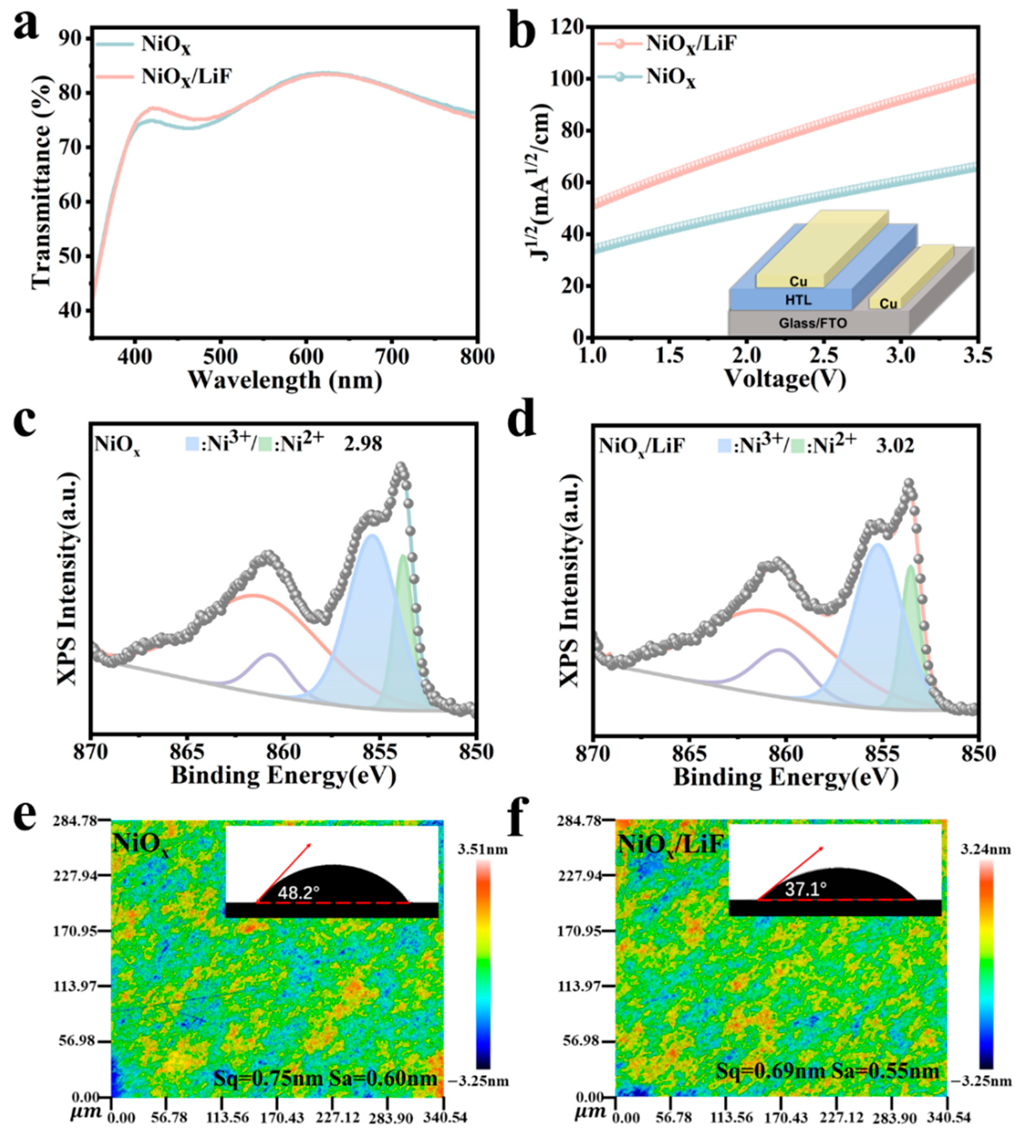
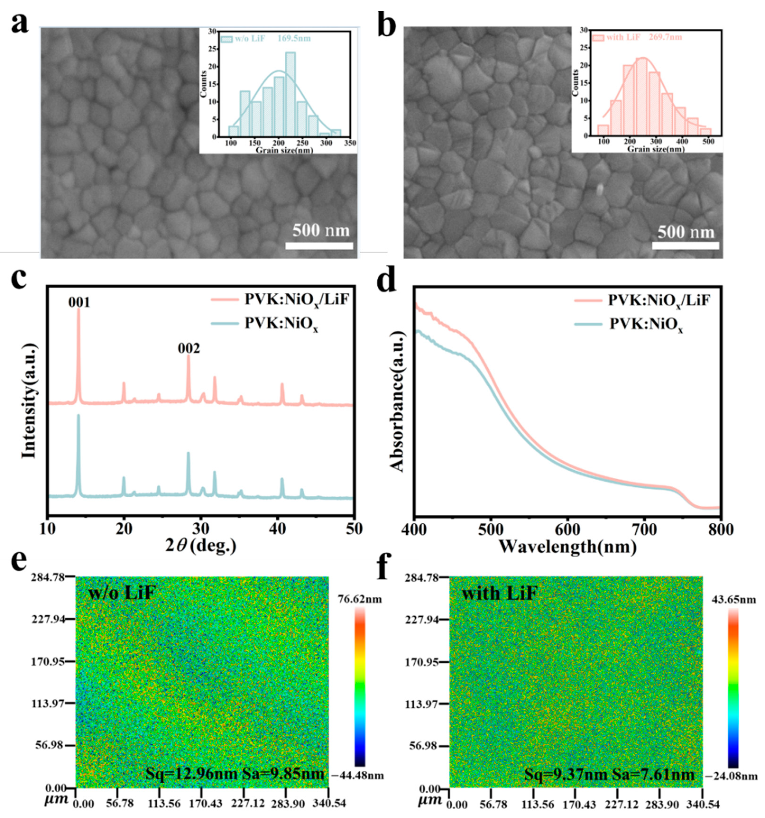
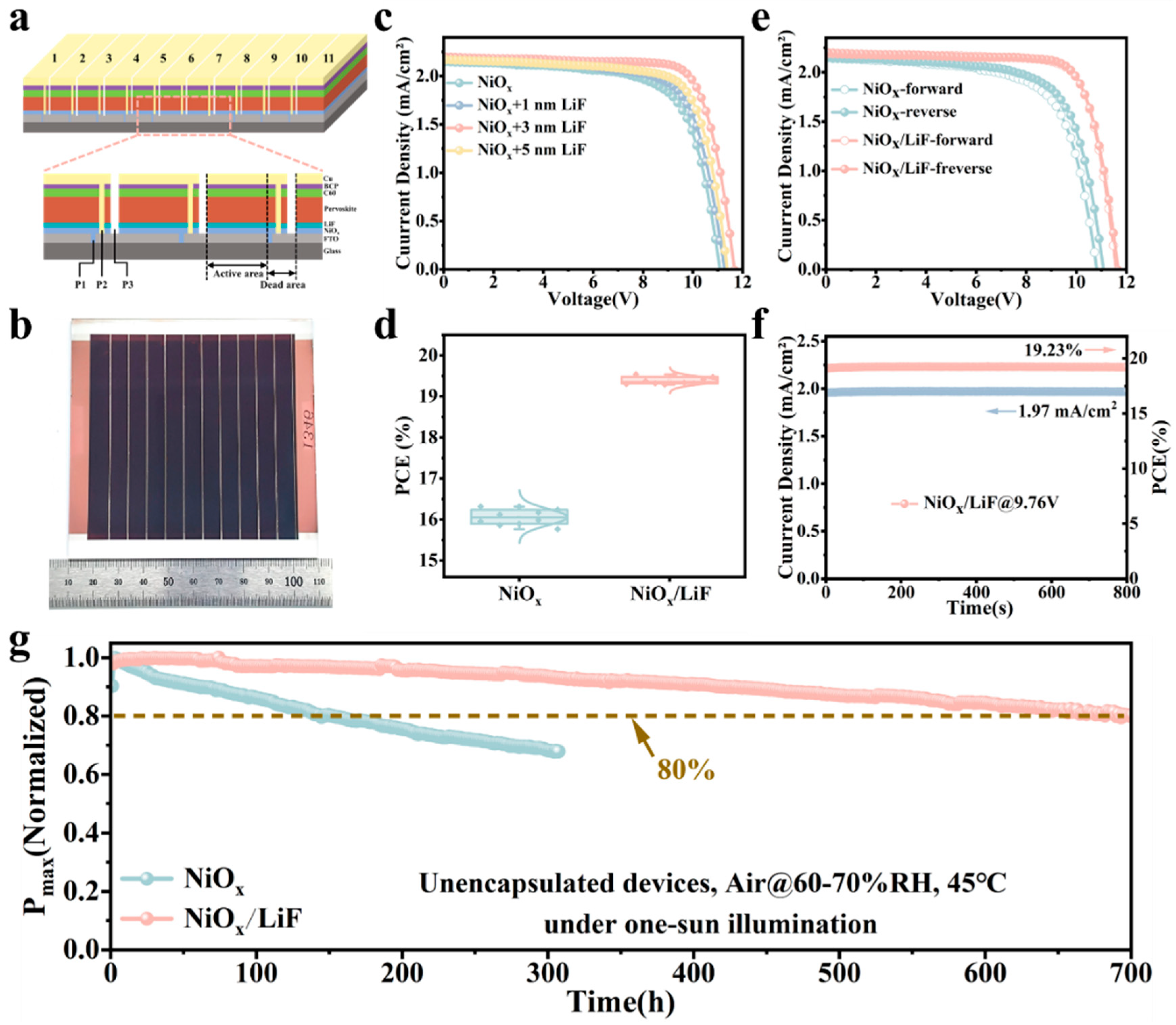
3. Results and Discussion

To assess whether the deposition of LiF impacts the transmittance of NiOx films, we characterized the films using ultraviolet–visible (UV-Vis) transmission spectroscopy. The NiOx/LiF films exhibit transmission spectra similar to that of pristine NiOx (Figure S1). Notably, the NiOx film with 3 nm of LiF displays maximum transmittance in the 400–550 nm range (Figure 1a). This enhanced transmittance is attributed to a reduction in surface roughness (to be elaborated later), which decreases light scattering and reflection loss, ultimately benefiting light absorption by the perovskite layer [22]. To investigate the influence of deposited LiF on the electrical properties of the NiOx films, we fabricated devices with the structure FTO/HTL/Cu and measured the hole mobility and conductivity of both NiOx and NiOx/LiF films using the space-charge-limited current (SCLC) method [23]. We employed the Mott–Schottky equation (Equation (1)) to fit the measured current–voltage (J–V) curves of the devices, enabling the calculation of hole mobility for the films [24].
J = 9 ε 0 ε r V 2 8 L 3
Here, J represents current density, μ represents hole mobility, ε 0 represents the vacuum permittivity, ε r represents the dielectric constant of NiOx, L represents the thickness of the NiOx film, and V represents the applied voltage to the device. As shown in Figure 1b, the hole mobilities of the NiOx film and NiOx/LiF film are 1.27 × 10⁻⁴ cm2V−1 s−1 and 1.91 × 10⁻⁴ cm2V−1 s−1, respectively. Clearly, the incorporation of LiF enhances the hole mobility of the NiOx film, thereby facilitating hole transport. Additionally, we calculated the conductivity of the NiOx films using Equation (2) as follows [25]:
σ = d A R
where σ is the conductivity, d is the thickness of the NiOx film, A is the active area, and R represents the resistance determined from the I–V curves of the NiOx or NiOx/LiF films. It can be calculated that the conductivities of the NiOx and NiOx/LiF films are 4.77 × 10⁻⁶ S/cm and 1.18 × 10⁻⁵ S/cm, respectively (Figure S2). This enhancement in conductivity is advantageous for reducing recombination losses of electrons and holes.
To investigate the mechanism by which deposited LiF enhances the conductivity and hole mobility of NiOx films, we conducted XPS analysis on the surfaces of both NiOx and NiOx/LiF films to study their elemental chemical states [10,26]. As shown in Figure 1c,d, we performed Lorentz–Gaussian peak fitting on the Ni2p3/2 peaks of both the NiOx and NiOx/LiF films. The peak at 854 eV corresponds to Ni2+, while the peak at 855 eV is attributed to Ni3+ induced by Ni2+ vacancies. Notably, the ratio of Ni3+/Ni2+ increases from 2.98 to 3.02, which suggests that Li+ has been incorporated into the NiOx matrix, leading to an improvement in conductivity and mobility [27]. Additionally, the X-ray diffraction (XRD) results for both NiOx and NiOx/LiF films indicate that they have the same crystalline phase structure (Figure S3). However, the XRD peaks of the NiOx/LiF film exhibit a blue shift, confirming that Li⁺ incorporates into the lattice of NiOx20. The relationship between homogeneous and heterogeneous nucleation indicates that the wettability of the substrate influences the nucleation and crystallization of the deposited perovskite, as illustrated in Equation (3) [28,29]:
G h e t e r o g e n e o u s = G h o m o g e n e o u s × 2 + cos θ 1 cos θ 2 4
where G h e t e r o g e n e o u s represents the nucleation free energy and θ represents the contact angle of the solid/liquid interface. As illustrated in Figure 1e,f the NiOx/LiF film surface exhibits slightly lower root mean square roughness (Sq = 0.69 nm) and arithmetic mean roughness (Sa = 0.55 nm) compared to the NiOx film, which has a root mean square roughness of Sq = 0.75 nm and an arithmetic mean roughness of Sa = 0.60 nm. We also measured the contact angle, and the results exhibit that the contact angle of the NiOx film is 48.2°, while that of the NiOx/LiF film is significantly reduced to 37.1°. This reduction in contact angle and roughness indicates that the perovskite precursor solution adheres better to the NiOx/LiF substrate, which lowers the energy barrier for perovskite nucleation and facilitates the formation of high-quality perovskite films [30].
Therefore, to observe the changes in the prepared perovskite films, we examined the morphology of the perovskite films deposited on NiOx and NiOx/LiF substrates using scanning electron microscopy (SEM) [31]. As shown in Figure 2a,b, the perovskite films deposited on both substrates exhibit similar morphologies and have dense polycrystalline grains, ensuring effective light absorption [32]. However, particle size analysis from the SEM images reveals that the average grain size of the perovskite film deposited on the NiOx substrate is 169.5 nm, while that of the perovskite film on the NiOx/LiF substrate significantly increases to 269.7 nm. This increase in grain size helps reduce the defect density in the perovskite films, improves their crystallization quality, and thereby enhances their optoelectronic performance and stability [33,34].
The improvement in the crystallization quality of the perovskite films was further confirmed by XRD characterization. As shown in Figure 1c, there are two sharp diffraction peaks at 14.06° and 28.36°, corresponding to the (001) and (002) crystal planes of the perovskite [17]. Compared to the perovskite film deposited on NiOx, the intensity of diffraction peaks in the films deposited on NiOx/LiF significantly increases, indicating a substantial enhancement in crystallinity and a higher degree of preferred orientation. Additionally, photoluminescence (PL) and absorption spectra of the perovskite films reveal that, compared to the films deposited on NiOx, the PL and absorption intensities of the films on NiOx/LiF significantly increase (Figure 2d and Figure S4), demonstrating improved optical performance attributed to enhanced crystallization quality [35,36]. As shown in Figure 2e,f, the perovskite film deposited on NiOx/LiF exhibits a significant reduction in roughness compared to the film on NiOx, with Sq decreasing from 12.96 nm to 9.37 nm and Sa decreasing from 9.85 nm to 7.61 nm. This reduction in roughness indicates that the perovskite films on the NiOx/LiF substrate are smoother, which helps reduce interface defects and improve charge carrier transport efficiency [37], thereby enhancing the performance of the device.
The efficient transfer of photogenerated charge carriers between the hole transport layer and the perovskite layer is influenced by the energy level offset between their valence bands. This factor also significantly impacts the Voc of the PSCs. To elucidate the energy level changes in NiOx and NiOx/LiF, we analyzed the energy level structures of the films using UPS [38], as shown in Figure 3a. Here, Ecut-off represents the cut-off energy for secondary electrons, and Eonset denotes the energy difference between the valence band maximum (EVBM) and the Fermi level (Ef). The Ef and EVBM can be calculated using the following Equations (4) and (5), where 21.22 is the photon energy of HeI in electronvolts (eV) [39].
E f = 21.22 E c u t - o f f
E V B M = 21.22 ( E c u t - o f f E o n s e t )
Through the UPS spectra, the Ef and EVBM of NiOx films can be calculated as 4.81 eV and 5.27 eV, respectively. For the NiOx/LiF film, the Ef and EVBM values increase to 4.92 eV and 5.31 eV, respectively. The schematic in Figure 3b illustrates that after the incorporation of LiF, the valence band position of the NiOx film aligns more closely with that of the perovskite layer. This alignment suggests that the symmetry between the NiOx and perovskite layers has improved and the energy barrier has been reduced, facilitating rapid hole extraction at the NiOx/perovskite interface and decreasing energy losses, thereby optimizing the Voc of the PSCs [40]. Additionally, the energy gap between Ef and EVBM decreased from 0.46 eV to 0.39 eV, which helps to increase the hole concentration in NiOx and contributes to improvements in short-circuit current density (Jsc) and FF of the PSCs [41].
Furthermore, we investigated the interface carrier extraction and transport capabilities between the perovskite layer and NiOx layer using PL and time-resolved photoluminescence (TRPL) characterization [42,43]. Figure 3c,d display the PL and TRPL spectra, with irradiating fluorescence incident from the glass side. Compared to the perovskite film deposited on NiOx, the perovskite film deposited on NiOx/LiF exhibits significant PL quenching, indicating that the incorporation of LiF reduces charge carrier recombination at the interface, thereby enhancing hole extraction and transport via NiOx. To calculate the charge transfer kinetics between NiOx and the perovskite, a double-exponential function was employed to fit the TRPL curve, as described by the following equation:
I ( t ) = I 0 + A 1 e x p ( t τ 1 ) + A 2 e x p ( t τ 2 )
Here, A1 and A2 represent the decay amplitudes, while τ 1 and τ 2 correspond to the charge carriers quenched by the HTL and radiation recombination in the perovskite film. The parameters and results obtained from the fitting are presented in Table S1. The formula for calculating the average lifetime is τ a v e = ( A 1 τ 1 2 + A 2 τ 2 2 ) / ( A 1 τ 1 + A 2 τ 2 ) [44,45]. The results indicate that after the incorporation of LiF, τ 1 decreases from 2.46 ns to 1.29 ns, τ 2 decreases from 99.26 ns to 68.62 ns, and the average lifetime decreases from 95.00 ns to 65.20 ns. These changes demonstrate a significant enhancement in NiOx’s ability to extract holes from the perovskite, consistent with PL results [46]. This improvement can primarily be attributed to two factors: the enhanced crystallization quality of the perovskite film and the improved P-type performance of the NiOx film.
As shown in Figure 4a,b, we fabricated a typical inverted-structure PSM based on FTO/NiOx/perovskite/C60/BCP/Cu, with the perovskite layer prepared in air using a slot-die coating method. The PSM consists of 11 interconnected sub-cells, with an active area of 57.30 cm2. The area between sub-cells P1 and P3, termed the “dead area”, does not contribute to the photocurrent and has a width of approximately 800 μm (Figure S5), resulting in a geometric fill factor of 89.68% for the PSM. Figure 4c shows the impact of different LiF thicknesses on device performance, indicating that optimal performance is achieved with a deposition thickness of 3 nm. To verify the reproducibility of the performance enhancement, we fabricated 10 PSMs based on NiOx and NiOx/LiF, with the distribution of their photovoltaic parameters statistically presented in Figure 4d and Figure S6. These results demonstrate that after the incorporation of LiF, all parameters exhibit significant increases, reflecting the high reproducibility of device performance. Subsequently, the champion PSMs based on NiOx and NiOx/LiF were further measured using forward and reverse scans (Figure 4e). In the forward scan, the devices based on NiOx/LiF exhibit an increase in Voc from 10.81 V to 11.59 V, Jsc from 2.15 to 2.19 mA cm−2, and FF from 67.06% to 75.84%, resulting in an increase in PCE from 15.57% to 19.24%. In the reverse scan, Voc increases from 11.08 V to 11.67 V, Jsc from 2.15 to 2.20 mA cm−2, and FF from 68.53% to 76.17%, and the resulting PCE increases from 16.33% to 19.54%. The improvement in PCE is primarily attributed to enhanced conductivity of NiOx, better energy level alignment with the perovskite layer, and improved crystallization quality of the perovskite film. The hysteresis factor of the devices based on NiOx/LiF is significantly reduced, mainly due to the considerable enhancement in carrier transport at the NiOx/perovskite interface [39]. Furthermore, the champion PSM based on NiOx/LiF maintains maximum output voltage for 800 s, with results showing that the output photocurrent density stabilizes at 1.97 mA cm⁻², corresponding to a stable PCE of 19.23% (Figure 4f). In order to evaluate the impact of LiF incorporation on the stability of the PSM, unencapsulated devices were placed in an environment with 60–70% relative humidity at 45 °C, and maximum power point tracking (MPPT) tests were conducted under white light-emitting diode (LED) illumination (equivalent to one-sunlight intensity) [22]. According to the results presented in Figure 4g, the NiOx/LiF-based devices maintain 80% of their initial efficiency after continuous operation for 700 h, while the NiOx-based devices experience a 20% decrease in efficiency after only 150 h under the same testing conditions. The incorporation of LiF significantly improves module stability, primarily due to the enhanced quality of the perovskite film and reduced interface carrier recombination.

4. Conclusions

In summary, we employ a simple and cost-effective method to achieve efficient doping of NiOx by thermally evaporating LiF onto sputtered NiOx. After the incorporation of LiF, the ratio of Ni3⁺ to Ni2⁺ in NiOx increases from 2.98 to 3.02, indicating that the effective doping of Li+ has led to an improvement in the conductivity of NiOx. The reduction in the contact angle of the NiOx/LiF film enhances the wettability of the perovskite precursor solution on NiOx, thereby improving the crystallization quality of the deposited perovskite film. Additionally, the incorporation of LiF results in a significant increase in hole concentration in NiOx and brings its valence band position closer to that of the perovskite layer. This adjustment greatly enhances the efficiency of hole injection from the perovskite layer to the NiOx and reduces energy loss during transport, improving the Voc and FF of the devices. Based on the improved P-type performance of NiOx and enhanced perovskite crystallization quality, the resulting PSM achieves an exceptional PCE of 19.54%. Furthermore, compared to the PSM based on NiOx, the unencapsulated LiF-incorporated PSM maintains 80% of its initial efficiency after 700 h of continuous illumination, while the efficiency of the NiOx-based PSM decreases by 20% after only 150 h, demonstrating the significant improvement in the stability of the NiOx/LiF-based PSM.

Supplementary Materials

The following supporting information can be downloaded at https://www.mdpi.com/article/10.3390/sym16101357/s1, Figure S1: the UV-Vis transmittance spectra of NiOx and NiOx/LiF films with different thicknesses of LiF. Figure S2: The I–V characterization of FTO/NiOx/Cu and FTO/NiOx/LiF/Cu device structures. Figure S3: XRD patterns of NiOx and NiOx/LiF films. Figure S4: The PL spectral of perovskite films deposited on NiOx and NiOx/LiF. Figure S5: Optical microscope images of the dead zone in the perovskite solar module. Figure S6: Voc, Jsc, FF, and PCE statistical diagrams of the NiOx-based device and NiOx/LiF-based device (photovoltaic parameters from 10 devices). Table S1: The PL decay curves of perovskite films deposited on NiOx and NiOx/LiF films.

Author Contributions

Conceptualization, L.W., X.L., and S.L.; methodology, L.W. and S.Y.; software, X.L., F.Q., and Z.K.; validation, L.W. and S.Y.; formal analysis, X.L. and F.Q.; investigation, L.W. and Z.K.; resources, X.L. and Z.K.; data curation, F.Q. and S.L.; writing—original draft preparation, L.W. and X.L.; writing—review and editing, L.W., S.Y., and S.L.; visualization, S.Y. and Z.K.; supervision, S.L.; project administration, Z.K. and S.L.; funding acquisition, S.L. All authors have read and agreed to the published version of the manuscript.

Funding

This research was funded by the Creative Research Groups of the National Natural Science Foundation of Sichuan Province (Grant No. 2023NSFSC1973), the National Natural Science Foundation of China (Grant Nos. 62104028 and 62174021), the Natural Science Foundation of Sichuan Province (Grant No. 2022NSFSC0899), the Sichuan Science and Technology Program (Grant No. MZGC20230008), and the China Postdoctoral Science Foundation (Grant No. 2021M700689).

Data Availability Statement

Data are contained within the article and Supplementary Materials.

Acknowledgments

The authors express their gratitude for the support from the Sichuan Province Key Laboratory of Display Science and Technology.

Conflicts of Interest

The authors declare no conflicts of interest.

References

  1. Liu, S.; Li, J.; Xiao, W.; Chen, R.; Sun, Z.; Zhang, Y.; Lei, X.; Hu, S.; Kober-Czerny, M.; Wang, J.; et al. Buried interface molecular hybrid for inverted perovskite solar cells. Nature 2024, 632, 536–542. [Google Scholar] [CrossRef] [PubMed]
  2. Zhao, X.; Zhang, P.; Liu, T.; Tian, B.; Jiang, Y.; Zhang, J.; Tang, Y.; Li, B.; Xue, M.; Zhang, W.; et al. Operationally stable perovskite solar modules enabled by vapor-phase fluoride treatment. Science 2024, 385, 433–438. [Google Scholar] [CrossRef] [PubMed]
  3. Zhang, Z.; Li, M.; Li, R.; Zhuang, X.; Wang, C.; Shang, X.; He, D.; Chen, J.; Chen, C. Suppressing Ion Migration by Synergistic Engineering of Anion and Cation toward High-Performance Inverted Perovskite Solar Cells and Modules. Adv. Mater. 2024, 36, 2313860. [Google Scholar] [CrossRef] [PubMed]
  4. Zhumagali, S.; Isikgor, F.H.; Maity, P.; Yin, J.; Ugur, E.; De Bastiani, M.; Subbiah, A.S.; Mirabelli, A.J.; Azmi, R.; Harrison, G.T.; et al. Linked Nickel Oxide/Perovskite Interface Passivation for High-Performance Textured Monolithic Tandem Solar Cells. Adv. Energy Mater. 2021, 11, 2101662. [Google Scholar] [CrossRef]
  5. Wang, L.; Zhang, T.; Yuan, S.; Qian, F.; Li, X.; Zheng, H.; Huang, J.; Li, S. Over 19% Efficiency Perovskite Solar Modules by Simultaneously Suppressing Cation Deprotonation and Iodide Oxidation. ACS Appl. Mater. Interfaces 2024, 16, 4751–4762. [Google Scholar] [CrossRef]
  6. Mao, L.; Yang, T.; Zhang, H.; Shi, J.; Hu, Y.; Zeng, P.; Li, F.; Gong, J.; Fang, X.; Sun, Y.; et al. Fully Textured, Production-Line Compatible Monolithic Perovskite/Silicon Tandem Solar Cells Approaching 29% Efficiency. Adv. Mater. 2022, 34, 2206193. [Google Scholar] [CrossRef]
  7. Wu, Y.; Zheng, P.; Peng, J.; Xu, M.; Chen, Y.; Surve, S.; Lu, T.; Anh Dinh, B.; Li, N.; Liang, W.; et al. 27.6% Perovskite/c-Si Tandem Solar Cells Using Industrial Fabricated TOPCon Device. Adv. Energy Mater. 2022, 12, 2200821. [Google Scholar] [CrossRef]
  8. Yang, Z.; Zhang, W.; Wu, S.; Zhu, H.; Liu, Z.; Liu, Z.; Jiang, Z.; Chen, R.; Zhou, J.; Lu, Q.; et al. Slot-die coating large-area formamidinium-cesium perovskite film for efficient and stable parallel solar module. Sci. Adv. 2021, 7, eabg3749. [Google Scholar] [CrossRef]
  9. Zhou, Y.; Huang, X.; Zhang, J.; Zhang, L.; Wu, H.; Zhou, Y.; Wang, Y.; Wang, Y.; Fu, W.; Chen, H. Interfacial Modification of NiOx for Highly Efficient and Stable Inverted Perovskite Solar Cells. Adv. Energy Mater. 2024, 14, 2400616. [Google Scholar] [CrossRef]
  10. Yu, S.; Xiong, Z.; Zhou, H.; Zhang, Q.; Wang, Z.; Ma, F.; Qu, Z.; Zhao, Y.; Chu, X.; Zhang, X.; et al. Homogenized NiOx nanoparticles for improved hole transport in inverted perovskite solar cells. Science 2023, 382, 1399–1404. [Google Scholar] [CrossRef]
  11. Chen, W.; Liu, F.Z.; Feng, X.Y.; Djurisic, A.B.; Chan, W.K.; He, Z.B. Cesium Doped NiOx as an Efficient Hole Extraction Layer for Inverted Planar Perovskite Solar Cells. Adv. Energy Mater. 2017, 7, 1700722. [Google Scholar] [CrossRef]
  12. Yao, K.; Li, F.; He, Q.Q.; Wang, X.F.; Jiang, Y.H.; Huang, H.T.; Jen, A.K.Y. A copper-doped nickel oxide bilayer for enhancing efficiency and stability of hysteresis-free inverted mesoporous perovskite solar cells. Nano Energy 2017, 40, 155–162. [Google Scholar] [CrossRef]
  13. Sun, X.; Zhang, C.; Gao, D.; Zhang, S.; Li, B.; Gong, J.; Li, S.; Xiao, S.; Zhu, Z.; Li, Z.A. Boosting Efficiency and Stability of NiOx-Based Inverted Perovskite Solar Cells Through D-A Type Semiconductor Interface Modulation. Adv. Funct. Mater. 2024, 34, 2315157. [Google Scholar] [CrossRef]
  14. Li, B.; Zhang, C.L.; Gao, D.P.; Sun, X.L.; Zhang, S.F.; Li, Z.; Gong, J.Q.; Li, S.; Zhu, Z.L. Suppressing Oxidation at Perovskite-NiOx Interface for Efficient and Stable Tin Perovskite Solar Cells. Adv. Mater. 2024, 36, 2309768. [Google Scholar] [CrossRef]
  15. Pu, X.; Zhao, J.; Li, Y.; Zhang, Y.; Loi, H.-L.; Wang, T.; Chen, H.; He, X.; Yang, J.; Ma, X.; et al. Stable NiOx-based inverted perovskite solar cells achieved by passivation of multifunctional star polymer. Nano Energy 2023, 112, 108506. [Google Scholar] [CrossRef]
  16. Li, H.; Zhang, C.; Gong, C.; Zhang, D.; Zhang, H.; Zhuang, Q.; Yu, X.; Gong, S.; Chen, X.; Yang, J.; et al. 2D/3D heterojunction engineering at the buried interface towards high-performance inverted methylammonium-free perovskite solar cells. Nat. Energy 2023, 8, 946–955. [Google Scholar] [CrossRef]
  17. Cao, Q.; Wang, T.; Pu, X.; He, X.; Xiao, M.; Chen, H.; Zhuang, L.; Wei, Q.; Loi, H.-L.; Guo, P.; et al. Co-Self-Assembled Monolayers Modified NiOx for Stable Inverted Perovskite Solar Cells. Adv. Mater. 2024, 36, 2311970. [Google Scholar] [CrossRef]
  18. Li, Z.; Sun, X.; Zheng, X.; Li, B.; Gao, D.; Zhang, S.; Wu, X.; Li, S.; Gong, J.; Luther, J.M.; et al. Stabilized hole-selective layer for high-performance inverted p-i-n perovskite solar cells. Science 2023, 382, 284–289. [Google Scholar] [CrossRef]
  19. Tang, H.; Shen, Z.; Shen, Y.; Yan, G.; Wang, Y.; Han, Q.; Han, L. Reinforcing self-assembly of hole transport molecules for stable inverted perovskite solar cells. Science 2024, 383, 1236–1240. [Google Scholar] [CrossRef]
  20. Niu, T.; Zhu, W.; Zhang, Y.; Xue, Q.; Jiao, X.; Wang, Z.; Xie, Y.-M.; Li, P.; Chen, R.; Huang, F.; et al. D-A-π-A-D-type Dopant-free Hole Transport Material for Low-Cost, Efficient, and Stable Perovskite Solar Cells. Joule 2021, 5, 249–269. [Google Scholar] [CrossRef]
  21. Kotta, A.; Seo, I.; Shin, H.-S.; Seo, H.-K. Room-temperature processed hole-transport layer in flexible inverted perovskite solar cell module. Chem. Eng. J. 2022, 435, 134805. [Google Scholar] [CrossRef]
  22. Wang, L.; Qian, F.; Zhang, T.; Zheng, H.; Li, X.; Lan, T.; Xu, Q.; Zhang, P.; Li, S.J.E.; Science, E. Electrophilic Molecule-Induced π-π Interactions Reduce Energy Disorder of Hole Transport Layer for Highly Efficient Perovskite Solar Modules. Energy Environ. Sci. 2024. [Google Scholar] [CrossRef]
  23. Jing, P.; Zhou, X.; Xu, Z.; Xu, Z. Numerical and experimental investigation on photothermal performance of polyimide/high-electrical-performance-coating composite films considering surface roughness. J. Therm. Sci. 2022, 31, 1206–1219. [Google Scholar] [CrossRef]
  24. Bai, Y.; Zhou, Z.; Xue, Q.; Liu, C.; Li, N.; Tang, H.; Zhang, J.; Xia, X.; Zhang, J.; Lu, X.; et al. Dopant-Free Bithiophene-Imide-Based Polymeric Hole-Transporting Materials for Efficient and Stable Perovskite Solar Cells. Adv. Mater. 2022, 34, 2110587. [Google Scholar] [CrossRef] [PubMed]
  25. Chen, H.; Yang, J.; Cao, Q.; Wang, T.; Pu, X.; He, X.; Chen, X.; Li, X. π-Interactions suppression of buried interface defects for efficient and stable inverted perovskite solar cells. Nano Energy 2023, 117, 108883. [Google Scholar] [CrossRef]
  26. Wang, H.; Zhang, W.; Wang, B.; Yan, Z.; Chen, C.; Hua, Y.; Wu, T.; Wang, L.; Xu, H.; Cheng, M. Modulating buried interface with multi-fluorine containing organic molecule toward efficient NiOx-based inverted perovskite solar cell. Nano Energy 2023, 111, 108363. [Google Scholar] [CrossRef]
  27. Cao, F.; Cheng, F.; Huang, X.; Dai, X.; Tang, Z.; Nie, S.; Yin, J.; Li, J.; Zheng, N.; Wu, B. Synergistic Effect between NiOx and P3HT Enabling Efficient and Stable Hole Transport Pathways for Regular Perovskite Photovoltaics. Adv. Funct. Mater. 2022, 32, 2201423. [Google Scholar] [CrossRef]
  28. Liu, H.; Li, C.; Dong, J.; Dai, Y.; Wang, P.; Shi, B.; Zhao, Y.; Zhang, X. Indium Iodide Additive Realizing Efficient Mixed Sn-Pb Perovskite Solar Cells. Adv. Energy Mater. 2024, 14, 202304234. [Google Scholar] [CrossRef]
  29. Barua, P.; Hwang, I. Bulk Perovskite Crystal Properties Determined by Heterogeneous Nucleation and Growth. Materials 2023, 16, 29. [Google Scholar] [CrossRef]
  30. Alghamdi, A.R.M.; Yanagida, M.; Shirai, Y.; Andersson, G.G.; Miyano, K. Surface Passivation of Sputtered NiOx Using a SAM Interface Layer to Enhance the Performance of Perovskite Solar Cells. ACS Omega 2022, 7, 12147–12157. [Google Scholar] [CrossRef]
  31. Zhang, S.; Ye, F.; Wang, X.; Chen, R.; Zhang, H.; Zhan, L.; Jiang, X.; Li, Y.; Ji, X.; Liu, S.; et al. Minimizing buried interfacial defects for efficient inverted perovskite solar cells. Science 2023, 380, 404–409. [Google Scholar] [CrossRef] [PubMed]
  32. Zhang, T.; Wang, F.; Chen, H.; Qian, F.; Li, J.; Zheng, H.L.; Yuan, S.H.; Peng, X.F.; Wang, Y.F.; Huang, J.; et al. Synchronized B-site alloying for high-efficiency inorganic tin-lead perovskite solar cells. Appl. Phys. Rev. 2023, 10, 11. [Google Scholar] [CrossRef]
  33. Cao, Y.; Yan, N.; Wang, M.Z.; Qi, D.Y.; Zhang, J.F.; Chen, X.; Qin, R.; Xiao, F.W.; Zhao, G.T.; Liu, Y.C.; et al. Designed Additive to Regulated Crystallization for High Performance Perovskite Solar Cell. Angew. Chem. Int. Ed. 2024, 9, e202404401. [Google Scholar]
  34. Li, G.; Su, Z.; Canil, L.; Hughes, D.; Aldamasy, M.H.; Dagar, J.; Trofimov, S.; Wang, L.; Zuo, W.; Jerónimo-Rendon, J.J.; et al. Highly efficient p-i-n perovskite solar cells that endure temperature variations. Science 2023, 379, 399–403. [Google Scholar] [CrossRef] [PubMed]
  35. Zhai, P.; Ren, L.X.; Zhang, Y.R.; Xu, Z.; Wu, Y.; Zhao, K.; Zhang, L.; Liu, S.Z. Performance-limiting formation kinetics in green water-processed perovskite solar cells. Energy Environ. Science 2023, 16, 3014–3024. [Google Scholar]
  36. Su, L. Growth of a Sub-Centimeter-Sized CsPbBr3 Bulk Single Crystal Using an Anti-Solvent Precipitation Method. Symmetry 2024, 16, 332. [Google Scholar] [CrossRef]
  37. Wu, S.Y.; Lin, S.Y.; Shi, Z.Q.; Guo, D.E.; Huang, H.; Zhou, X.F.; Zhang, D.; Zhou, K.C.; Zhang, W.H.; Hu, Y.; et al. Improved Thermal Stability and Film Uniformity of Halide Perovskite by Confinement Effect brought by Polymer Chains of Polyvinyl Pyrrolidone. Small 2023, 19, 11. [Google Scholar] [CrossRef] [PubMed]
  38. Liu, L.; Ma, Y.; Wang, Y.; Ma, Q.; Wang, Z.; Yang, Z.; Wan, M.; Mahmoudi, T.; Hahn, Y.-B.; Mai, Y. Hole-Transport Management Enables 23%-Efficient and Stable Inverted Perovskite Solar Cells with 84% Fill Factor. Nano-Micro Lett. 2023, 15, 117. [Google Scholar] [CrossRef]
  39. Jiang, C.; Qin, T.; Tan, L.; Li, H.; Zhou, J.; Li, M.; Dang, Z.-M.; Ding, L.; Xiong, Q.; Yi, C. Revealing the Hole and Electron Transport Dynamics in the Working Devices for Efficient Semitransparent Perovskite Solar Cells. Adv. Energy Mater. 2024, 14, 2304093. [Google Scholar] [CrossRef]
  40. Seo, J.H.; Kim, H.J.; Cho, S.N. Build-up of symmetry breaking using a titanium suboxide in bulk-heterojunction solar cells. Phys. Chem. Chem. Phys. 2012, 14, 4062–4065. [Google Scholar] [CrossRef]
  41. Xie, G.; Li, Q.; Lu, X.; Li, L. Tailoring p-Type Charge-Transfer-Doped Hole Transport Layer for All-Inorganic CsPbBr3 Perovskite Solar Cells. ACS Photonics 2024, 11, 3365–3374. [Google Scholar] [CrossRef]
  42. Tian, H.; Jiang, X.; Liu, X.; Sun, F.; Guo, X.; Li, C. Enhancing performances of inverted perovskite solar cells by modifying the buried interface with sodium copper chlorophyllin. Nano Energy 2024, 126, 109616. [Google Scholar] [CrossRef]
  43. Yuan, S.H.; Zhang, T.; Chen, H.; Ji, Y.; Hao, Y.H.; Zheng, H.L.; Wang, Y.F.; Chen, Z.D.; Chen, L.; Li, S.B. Dual-functional passivators for highly efficient and hydrophobic FA-based perovskite solar cells. Chem. Eng. J. 2022, 433, 9. [Google Scholar] [CrossRef]
  44. Zhang, T.; Qian, F.; Chen, H.; Zheng, H.L.; Wang, L.; Yuan, S.H.; Wu, Y.F.; Chen, Z.D.; Li, S.B. Critical role of post-treatment induced surface reconstruction for high performance inorganic tin-lead perovskite solar cells. Chem. Eng. J. 2024, 479, 9. [Google Scholar] [CrossRef]
  45. Zheng, H.L.; Peng, X.F.; Chen, T.X.; Zhang, T.; Yuan, S.H.; Wang, L.; Qian, F.; Huang, J.; Liu, X.D.; Chen, Z.D.; et al. Boosting efficiency and stability of 2D alternating cation perovskite solar cells via rational surface-modification: Marked passivation efficacy of anion. J. Energy Chem. 2023, 84, 354–362. [Google Scholar] [CrossRef]
  46. Qiu, J.; Mei, X.; Zhang, M.; Wang, G.; Zou, S.; Wen, L.; Huang, J.; Hua, Y.; Zhang, X. Dipolar Chemical Bridge Induced CsPbI3 Perovskite Solar Cells with 21.86% Efficiency. Angew. Chem. Int. Ed. 2024, 63, e202401751. [Google Scholar] [CrossRef]
Figure 1. (a) The UV-Vis transmittance spectra of NiOx and NiOx/LiF films. (b) The J–V curves of NiOx and NiOx/LiF films. Inset: The device structure of space-charge-limited hole-only devices. XPS spectra of the Ni 2p3/2 peak (c) in NiOx film and (d) in NiOx/LiF film. Surface roughness of (e) NiOx film and (f) NiOx/LiF film, with the contact angle images shown in the insets.
Symmetry 16 01357 g001
Figure 2. SEM images of perovskite films deposited on (a) NiOx film and (b) NiOx/LiF film. Inset: Statistical graphs of grain size distribution of perovskite films. (c) XRD patterns and (d) absorption spectra of perovskite films deposited on NiOx and NiOx/LiF films. Surface roughness maps of perovskite films deposited on (e) NiOx film and (f) NiOx/LiF film.
Symmetry 16 01357 g002
Figure 3. (a) The UPS results of NiOx and NiOx/LiF films. (b) Schematic energy levels of NiOx, NiOx/LiF, and perovskite layers. (c) PL and (d) TRPL spectra of perovskite films deposited on NiOx and NiOx/LiF films, with the laser incident from the glass side.
Symmetry 16 01357 g003
Figure 4. (a) Schematic diagram of the perovskite solar module with 11 sub-cells connected in series. (b) Photograph of the PSM with a substrate size of 10 cm × 10 cm and an active area of 57.30 cm2. (c) J–V curves of PSM based on different thicknesses of LiF. (d) PCE statistical diagrams of the NiOx-based and NiOx/LiF-based PSM. (e) J–V curves of the best-performing NiOx-based and NiOx/LiF-based PSM under forward and reverse scan conditions. (f) Steady-state output PCE measured at the maximum power point of the champion NiOx/LiF-based PSM. (g) MPPT curves of the unencapsulated NiOx-based and NiOx/LiF-based PSM under continuous one-sun illumination.
Symmetry 16 01357 g004
Disclaimer/Publisher’s Note: The statements, opinions and data contained in all publications are solely those of the individual author(s) and contributor(s) and not of MDPI and/or the editor(s). MDPI and/or the editor(s) disclaim responsibility for any injury to people or property resulting from any ideas, methods, instructions or products referred to in the content.

