Article

Miniaturized Coplanar Waveguide-Fed UWB Antenna for Wireless Applications

by
Maryam S. Jameel
1,
Yaqeen S. Mezaal
2,* and
Dogu Cagdas Atilla
1
1
Electrical and Computer Engineering Department, Altinbas University, Istanbul 34217, Turkey
2
Medical Instrumentation Engineering Department, Al-Esraa University College, Baghdad 10011, Iraq
*
Author to whom correspondence should be addressed.
Symmetry 2023, 15(3), 633; https://doi.org/10.3390/sym15030633
Submission received: 24 November 2022 / Revised: 1 February 2023 / Accepted: 22 February 2023 / Published: 2 March 2023
(This article belongs to the Special Issue Symmetry/Asymmetry in Wireless Communication and Sensor Networks)

Abstract

:
This study presents a compact ultra-wideband (UWB) antenna fed by a coplanar waveguide (CPW) with huge bandwidth for the demands of modern wireless communities. To overcome some technical limitations of the employed substrate and UWB antenna design, a slotted patch resonator was used to create and simulate this antenna based on Locked-Key topology. It has been printed on a 1.5 mm-thick FR4 substrate with a dielectric constant of 4.4. A feeder with characteristic impedances of 50 Ω has been employed. A CST electromagnetic simulator has been employed to simulate and analyze the antenna design. It is operated within the UWB spectrum with a bandwidth of 10.354 GHz, spanning 3.581 to 14 GHz. The overall surface area is 27 × 25 mm2. The gain and maximum efficiency within UWB are better than 3 dBi and 82%, respectively. The antenna is fabricated, and the simulated results are correlated with the measured ones. Finally, the equivalent circuit models for the antenna and rectifier circuit are simulated and measured.

1. Introduction

UWB antennas have been increasingly popular in recent years for wireless communities. The Federal Communications Commission (FCC) defines the UWB phenomenon as a radio system that spans more than 25 percent of the center frequency with a bandwidth greater than or equal to 500 MHz [1]. Typical properties of UWB antennas, including satisfactory S11 parameters, useful radiation patterns, tiny size, and cost-effectiveness, must be met through the antenna design [2]. The UWB technology advantages are high data rates, slight interference, reliability, cost-effectiveness, and low complexity. As the pulse time is a fraction of a millisecond, this method has one major drawback, including the need for precise receptor time synchronization. Radar, medical imaging, and military communications are just a few of the use areas for this technology [3]. UWB antennas with band rejection capabilities have recently been developed to reduce interference in wireless applications with limited bandwidth. Various slots can be inserted into the patch, feed, and ground plane to accomplish this approach [4]. A reduced antenna size to boost the bandwidth using a slot has been reported in [5]. New antenna structures are being sought to suit the strict requirements of smart gadgets compatible with current wireless communications [6,7].
The current work aims to project a new miniature UWB antenna with a huge UWB frequency range of 10.354 GHz. The FR4 substrate was employed to accomplish this antenna with a Locked-Key radiating patch and a CPW feeder with applicable electrical specifications. The gain and maximum efficiency within UWB are better than 3 dBi and 82%, respectively. The proposed antenna is smaller and has a wider frequency range than other UWB antennas that have been reported.

2. Literature Survey

The first CPW-fed antenna was reported in 1990. There are alternative designs, such as tapered slot antennas with the coplanar waveguide. The CPW microstrip antenna with rectangular slot, circular patch CPW-fed circularly polarized antenna, dielectric resonator antenna with dual-polarization, and miniature tapered-slot antenna can be employed for different applications. These suggested radiating elements are difficult to construct, and the bandwidths achieved are claimed to be inadequate and have limited uses. It is challenging to build a CPW-fed antenna with a larger bandwidth and an uncomplicated radiating structure with high efficiency and radiation patterns [8]. CPW and microstrip line feeders are two of the most used feeding strategies for monopole antennas. However, CPW feeding is preferred because the ground plane is similar to the radiator components.
In contrast to the microstrip line feeder, the CPW-fed antenna has a ground plane on upper radiation components. CPW-fed monolithic microwave integrated circuits can be easily combined with CPW, as reported in [9]. In [10], the implementation of a small, dual-notch band, CPW-fed UWB antenna has been proposed. The antenna has selectable notch bands between 4 and 5.78 GHz and 6.83 and 8.22 GHz. The proposed configuration is an iterated octagonal patch antenna built on a relatively inexpensive FR4 substrate. By means of a slotted patch resonator and a decreased ground plane constructed on a FR4 substrate, a new miniaturized UWB microstrip antenna with an overall dimension of 13 × 27.2 mm2 was designed. The planned antenna was simulated using a CST electromagnetic simulator, and it features three resonances of 3.1, 5.2, and 8.5 GHz with respective S11 values of −20.5, −21.8, and −22 dB, with the impedance bandwidth of 6.23 GHz. This antenna was fabricated and tested to verify input reflection results of the simulation, and the experimental consequences are commensurate with the simulated ones [11]. A strawberry artistic-shaped printed monopole (SAPM) antenna was designed with a single-layer frequency selective surface (FSS) as the metallic plate to increase the antenna’s gain. They used six cylinders to create the strawberry-shaped radiating element, resulting in an improved antenna UWB frequency range. On an FR4 substrate with CPW feeding, this antenna was projected with a bandwidth of 8.85 GHz (3.05–11.9 GHz) that covered the acceptable UWB frequency range. A 6.22 dB gain has been realized using the UWB SAPM antenna with the FSS reflector in the lower and upper bands. The antenna has a size of 61 × 61 × 1.6 mm3 in total. UWB and ground-penetrating radar (GPR) applications can benefit from the recommended antenna layout because of its directed and balanced far-field pattern [12]. An antenna with a size of 23.5 × 31 × 1.5 mm3 based on an FR4-epoxy substrate has been reported in [13]. The antenna’s measurements show that the frequency range of 1.76 to 11.07 GHz is operational and rejects the frequency range of 2.42 to 5.37 GHz with a satisfactorily measured input impedance. Simulated data further reveal that the antenna has constant radiation patterns with considerable gain and efficiency across the whole working spectrum, except for the notched band, which is not shown. Eventually, the suggested antenna can be a worthy choice for wireless communication systems. For personal wireless communication and UWB applications, a compact band-notched UWB antenna has been reported in [14]. The antenna operates on the UWB (3.1–10.6 GHz) and Bluetooth (2.4–2.484 GHz) frequency bands, with band-notch characteristics on the Wireless Local Area Network (WLAN) (5–6 GHz) frequency band. Utilizing a typical cylindrical patch and a reformed ground plane, the UWB frequency band has been realized. The Bluetooth frequency band has integrated utilizing a small resonator and capacitors. In addition, a standard slot resonator has been incorporated into the radiator to decrease the WLAN band interference within the UWB spectrum. Moreover, the antenna has a stable passband gain and a satisfactory radiation pattern. In [15], a small, lightweight, UWB-printed monopole antenna with enhanced gain and efficiency has been explained. The CPW was used to feed a jug-shaped radiator in this broadband-printed monopole antenna to create and evaluate the suggested antenna design technique. The designed UWB antenna is made from an inexpensive FR4 substrate for wireless communication systems. At its peak, the UWB antenna can cover the frequency range from 3 to 11 GHz with an output gain of 4.1 dBi. The paper in [16] examines studies that have increased antenna gain utilizing frequency-selective surface (FSS) approaches for UWB frequencies. The research landscape was mapped to taxonomy to identify the most effective antenna gain improvement strategy. This project also investigated FSS as a reflector at UWB frequencies to produce directional radiation. Due to its excellent capability for decreasing power loss in unsuitable antenna transmission zones and preventing interference from unwanted and discarded radiation, the FSS is well-suited for many uses. An ISM (2.4 GHz) and UWB (3.1–10.6 GHz) dual-spectrum, split-ring monopole with a low-profile design is shown in [17]. The monopole functions simultaneously in the industrial scientific medical (ISM) and UWB bands. To obtain the best performance in both bands, split-ring radiators with a circular cross-section have been used. Both rings of the structure are coupled to each other, resulting in quasi-resonant frequencies in the UWB range. Two radiators are combined into a single antenna element that resonates at the ISM band of 2.45 GHz owing to a small stub. For UWB applications, a new design of FSS unit cells is proposed for the directional CPW planar antenna with high gain [18]. Using the Mercedes artistic-shaped planar (MAP) antenna, the UWB antenna was designed. The antenna had a circular ring inserted with three straight legs to improve the antenna bandwidth. The simulated FSS is based on a circular loop topology integrated with two parallel conductive metallic patches. For frequencies ranging from 2.2 to 12.7 GHz, the FSS delivered a stopband filter response with a bandwidth of 10.5 GHz. In terms of physical size, the proposed FSS was only 5 mm-wide, 5 mm-high (including the antenna), and 1.6 mm-thick. In [19], this study proposed a small symmetrical broadband antenna for use with WLANs and WIMAX networks. The projected antenna is an octagonal radiator printed on the FR4 dielectric substrate with Vicsek fractal slots and a reduced ground plane, and its total dimensions are 50 × 50 × 1.6 mm3. CST and the CADFEKO electromagnetic solvers were used to simulate the antenna. The broadband bandwidth accommodates both the WiMAX and WLAN frequency bands, operating at 2.3/2.5/3.3/3.5/5/5.5 GHz and 3.6/2.4–2.5/4.9–5.9 GHz, respectively. The anticipated antenna has excellent efficiency at the resonant frequencies (88.5% and 84.6%, respectively), gain measurements of 2.78 and 5.32 dBi in the E-plane, and omnidirectional observed radiation patterns in the H-plane. There is a remarkable degree of concordance (almost 90%) between the findings of the simulation and the consequences of the measurements.

3. Antenna Design

The wireless communication industry heavily relies on microstrip antennas. Microstrip antennas provide several advantages due to their symmetrical and non-symmetrical planar shape, low cost, lightweight, and easy integration into arrays. Mobile radios and wireless communication are the most effective. A microstrip antenna is useful for applications requiring a low-profile antenna since it can quickly adapt to a given shape. A microstrip antenna’s most significant advantage is its ability to operate simultaneously at many frequencies [19,20]. It is preferable to use microstrip antennas, easily integrated into a particular design. Although a microstrip antenna can be designed using a variety of substrates, the frequency range from 1 to 100 GHz can only be applied to one substrate at a time [21]. A patch antenna comprises four pieces (patch, substrate, ground, and feed). Microstrip antennas include a substrate that acts as an appropriate gate to support the patch and ground plane. The antenna substrate or a flexible substrate made of flexible materials is used if the antenna must be put on a variable-shaped structure. Flexible microstrip patches have been widely used for industrial, scientific, and medical uses. Since the antennas must be flexible and bendable, making the substrate layer as thin as possible is better to allow for greater flexibility.
The bandwidth and gain of a microstrip patch antenna are reduced when the substrate thickness is reduced. The antenna’s return loss, bandwidth, and strength must be improved to overcome this disadvantage. Due to its limited bandwidth and poor power, the antenna has a few drawbacks. Patch antennas were designed in various shapes and sizes to increase the frequency range [22]. Changes in the ground plane and patch were also made to meet the gain and bandwidth requirements. The MPA’s bandwidth has been boosted by the extensive use of ground plane slots. A comprehensive range of frequencies can be generated by employing this technique [23,24,25].
CPW antennas have gained favor because of their ultra-wideband capabilities. Thus, they are commonly utilized in broadband and volume-limited applications. Figure 1 shows a schematic representation of the antenna’s proposed design based on the Locked-Key topology. The FR4 substrate with a relative dielectric constant of 4.4 and a 1.5 mm thickness was used to create this antenna, which features an etched round feed slot at the beginning of its feed path. The 3 mm-wide feeder with equal-sized side slots is similar to the keys for doors with a 50-ohm impedance value. The substrate’s dimensions were 25 mm-wide, 27 mm-long, and 1.5 mm-thick. The gap between the transmission line and the ground was 0.35 mm.
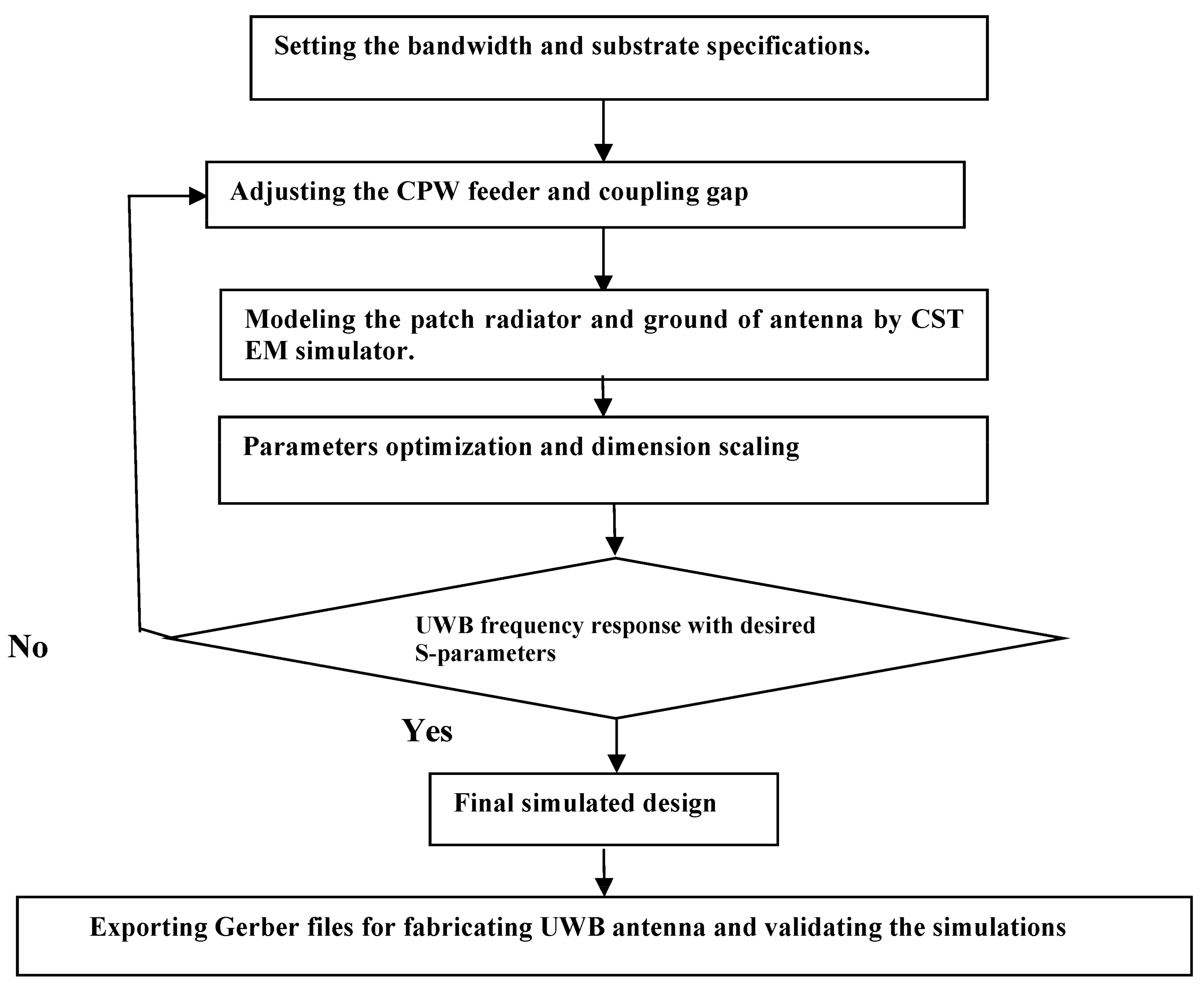
Figure 2 depicts the design and optimization procedures for the projected UWB antenna. Based on the ‘Trial and Error’ approach, the UWB frequency range and S11 parameter of the projected antenna can be adjusted by several trial steps to attain the planned band application by resizing the external antenna dimensions inversely proportional to the fundamental frequency. The slots, slits, size of the microstrip patch, and the ground can be employed as efficacious optimization predictors for the needed UWB frequency range.
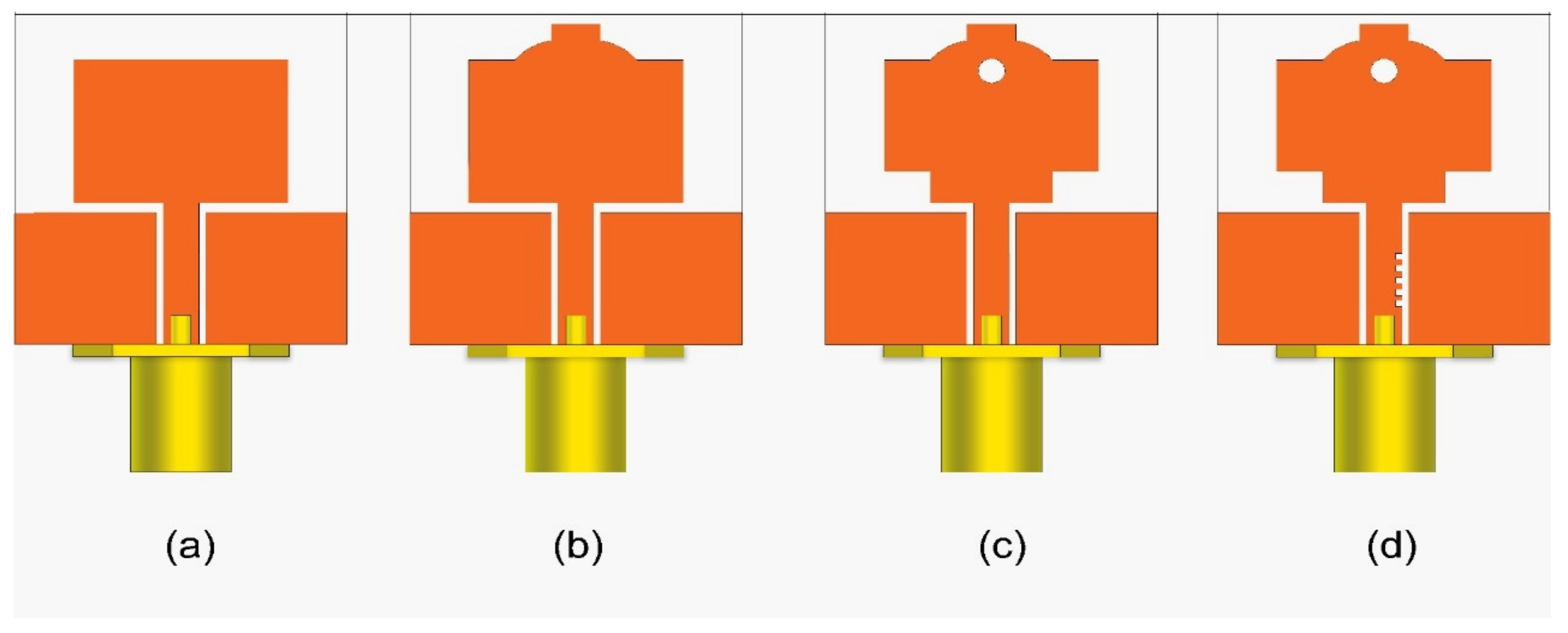
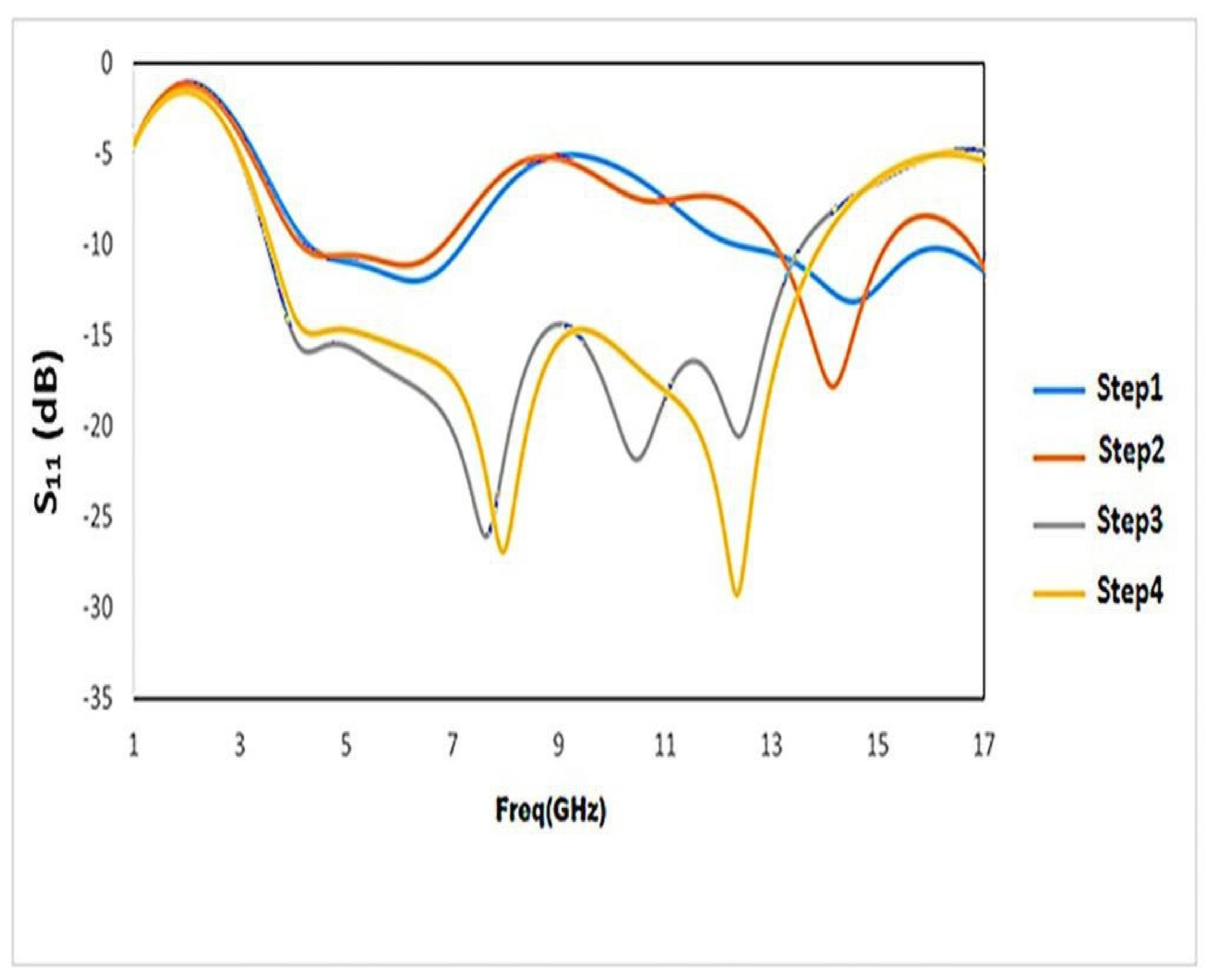
Accordingly, within the 1 to 17 GHz frequency range, the impact of several varieties of patch radiator on the input reflection performance of the CPW-fed antenna, as depicted in Figure 3, has been examined by adopting the same FR4 substrate material and dimensions. Accordingly, Figure 4 divulges that the patch radiator without slots, in Figure 3a,b, has a dual-band along with notches observed in frequency responses of Step 1 and 2, with a slight difference in bandwidth. On the other hand, for Steps 3 and 4, in Figure 3c,d, the effectual UWB responses are apparent based on patch shape deformation with the applied circle slot, but the antenna shows a relatively higher bandwidth in Step 4 (Locked-Key topology) than in Step 3 based on the effect of circle slots and teeth slits. Therefore, we selected this step to manufacture and measure the intended UWB antenna.
Based on the substrate width and length, the following equations were feasibly employed to evaluate the fundamental lower frequency (FL) for the projected UWB antenna:
FL = 0.53   C L sub     ε r + 1 2 = 0.49   C W sub     ε r + 1 2
where ε r signifies the relative dielectric constant, and c represents the speed of light. In terms of guided wavelength ( λ g ), the projected UWB antenna has a substrate size of about 0.53 λ g × 0.4 λ g at its lower frequencies of 3.581 GHz for the projected antenna.
Using the slotted patch radiator, the following equations can be used to determine the antenna’s width and length:
Wsub = 0.53   C 2   FL 2 ε r + 1
Lsub = 0.49   C 2   FL   2 ε r + 1
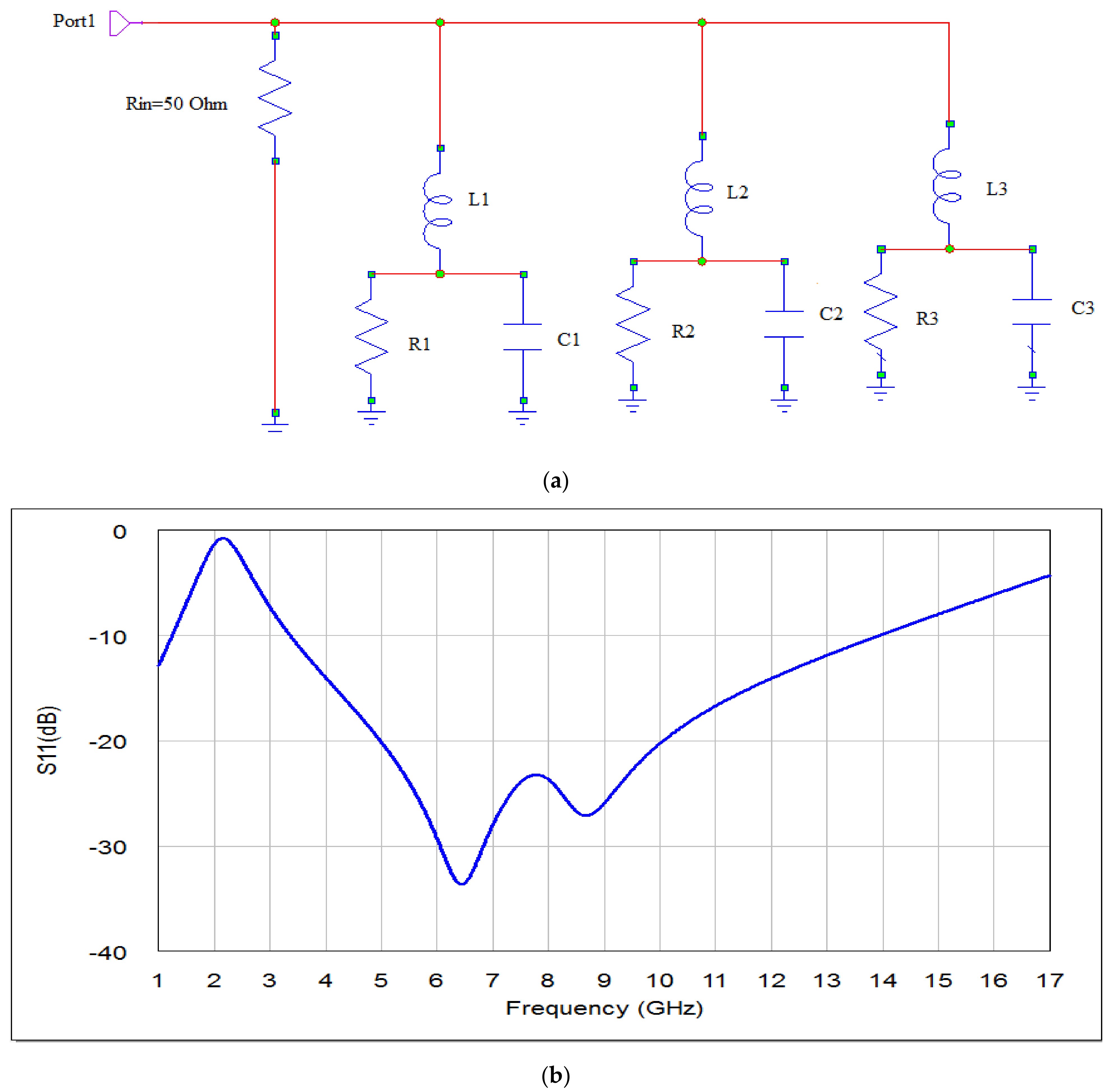
The RLC equivalent circuit for the designed UWB antenna and its input reflection response have been illustrated in Figure 5 using a microwave office simulator. The resistors are in parallel with the capacitors. Through changing the resistor magnitudes, the input reflection for a circuit model can be varied, while by changing the magnitudes for capacitors, the input reflection for the projected UWB antenna can be tuned. The first and last inductors can be employed to adjust the impedance bandwidth range. The impedance bandwidth is ranged from 3.4 to 14 GHz, which is highly similar to the planned bandwidth specification for the projected UWB antenna in this study.

4. Simulation Consequences and Discussion

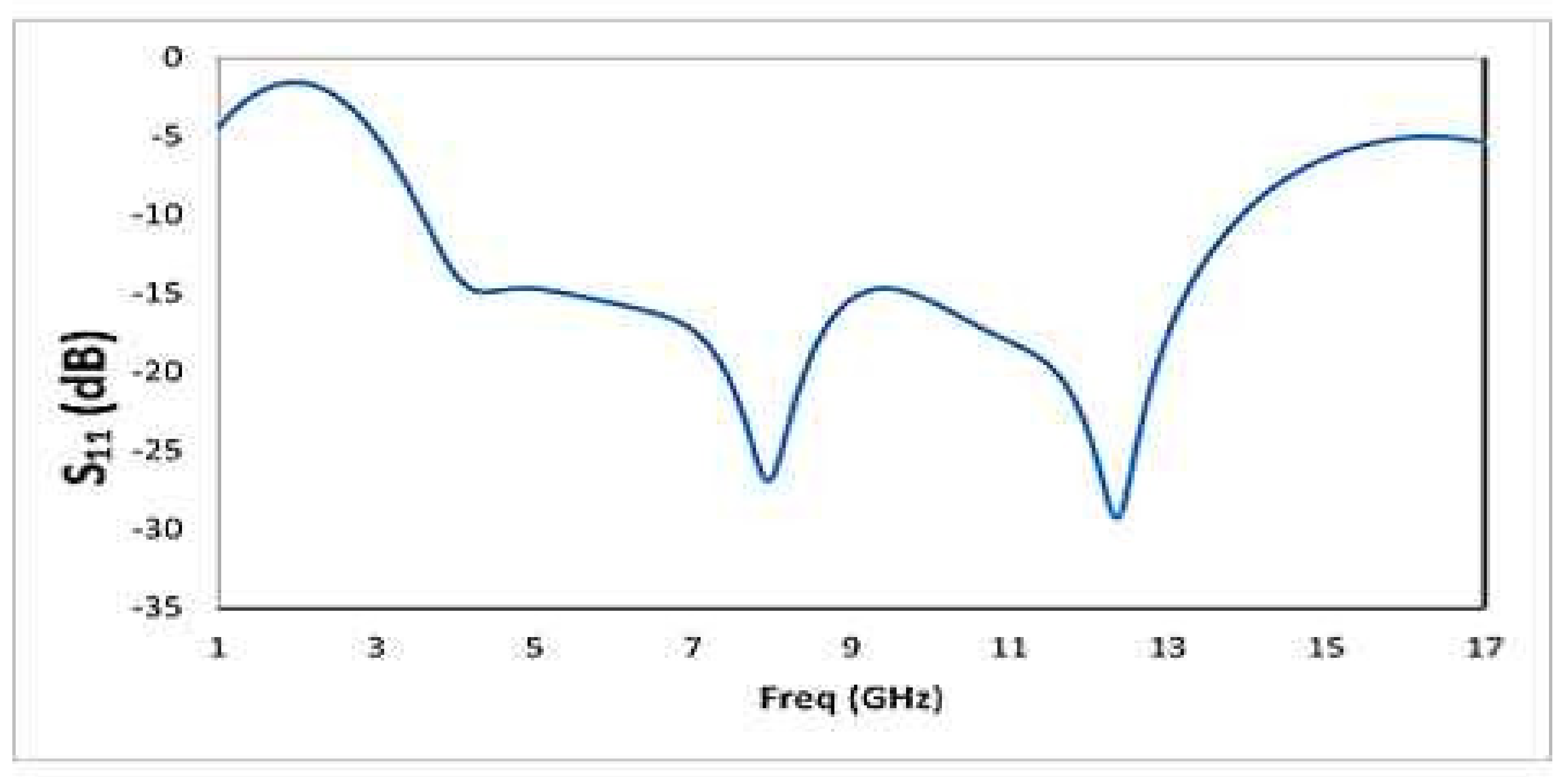
The CPW-fed antenna was designed and simulated using the CST simulator, which is frequently utilized for designing countless types of antennas. Under a bandwidth (BW) of 10.354 GHz, the central frequency was 8.76 GHz, as shown in Figure 6, with a satisfactory scattering S11 parameter.
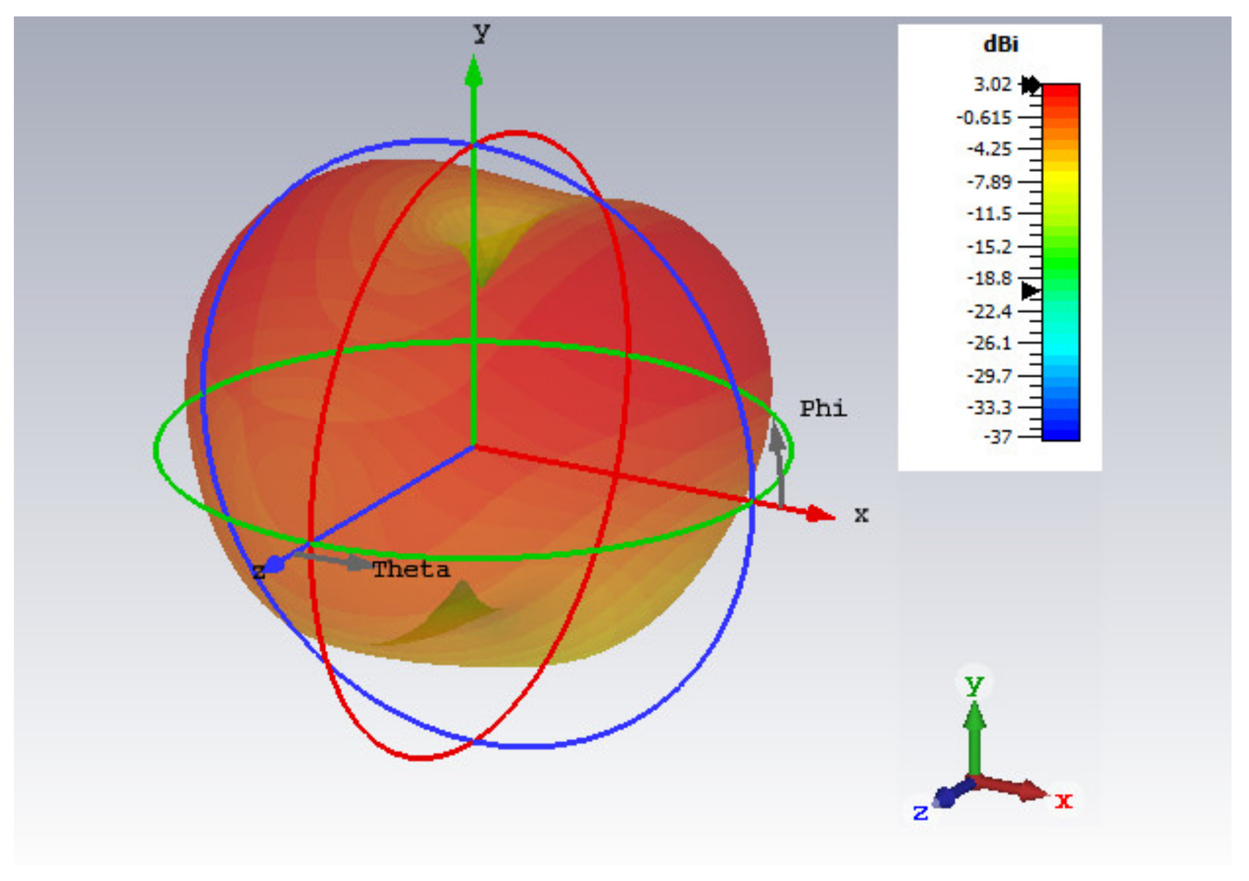
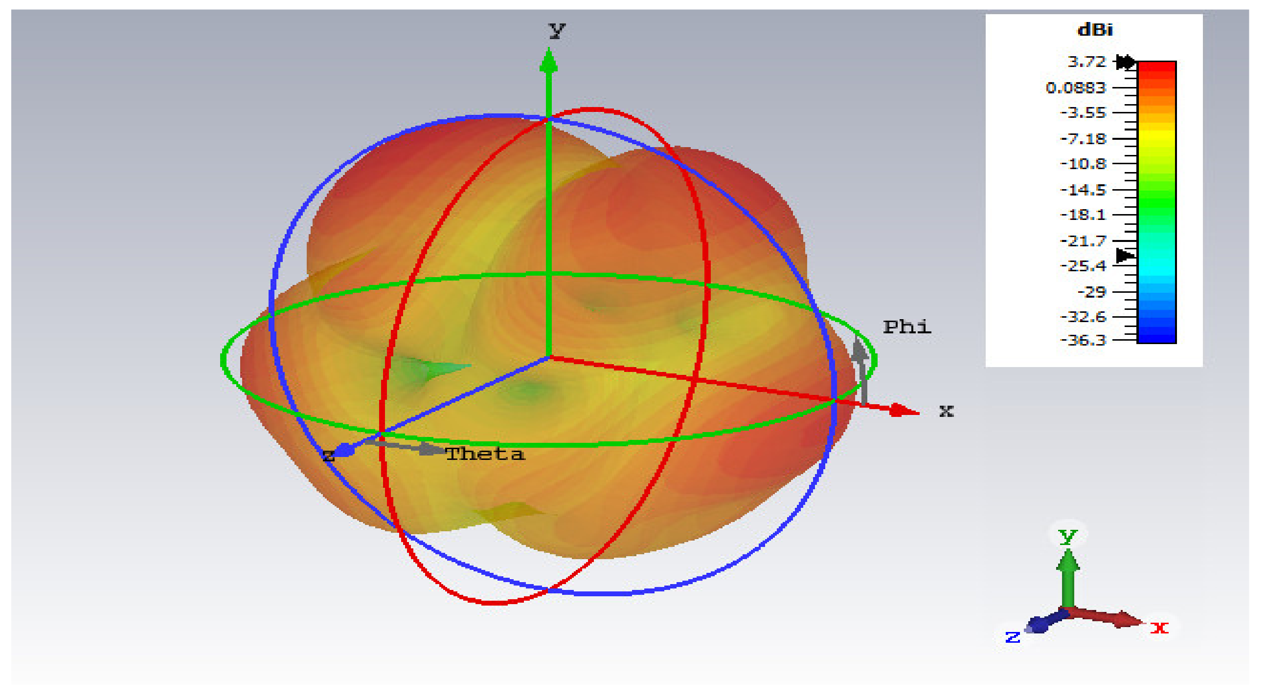
Figure 7 and Figure 8 show the 3D radiation patterns for the proposed UWB antenna with a maximum gain of 3.02 dBi at a resonant frequency of 8 GHz and with a maximum gain of 3.72 dBi at a resonant frequency of 12.2 GHz.
The surface current distribution in the regions of the designed UWB antenna at 3.58, 8.76, and 14 GHz is shown in Figure 9. At all resonant frequencies, the maximum magnetic strength was 69.5 A/m, and the effective regions were in the feeder, at the patch radiator’s base.
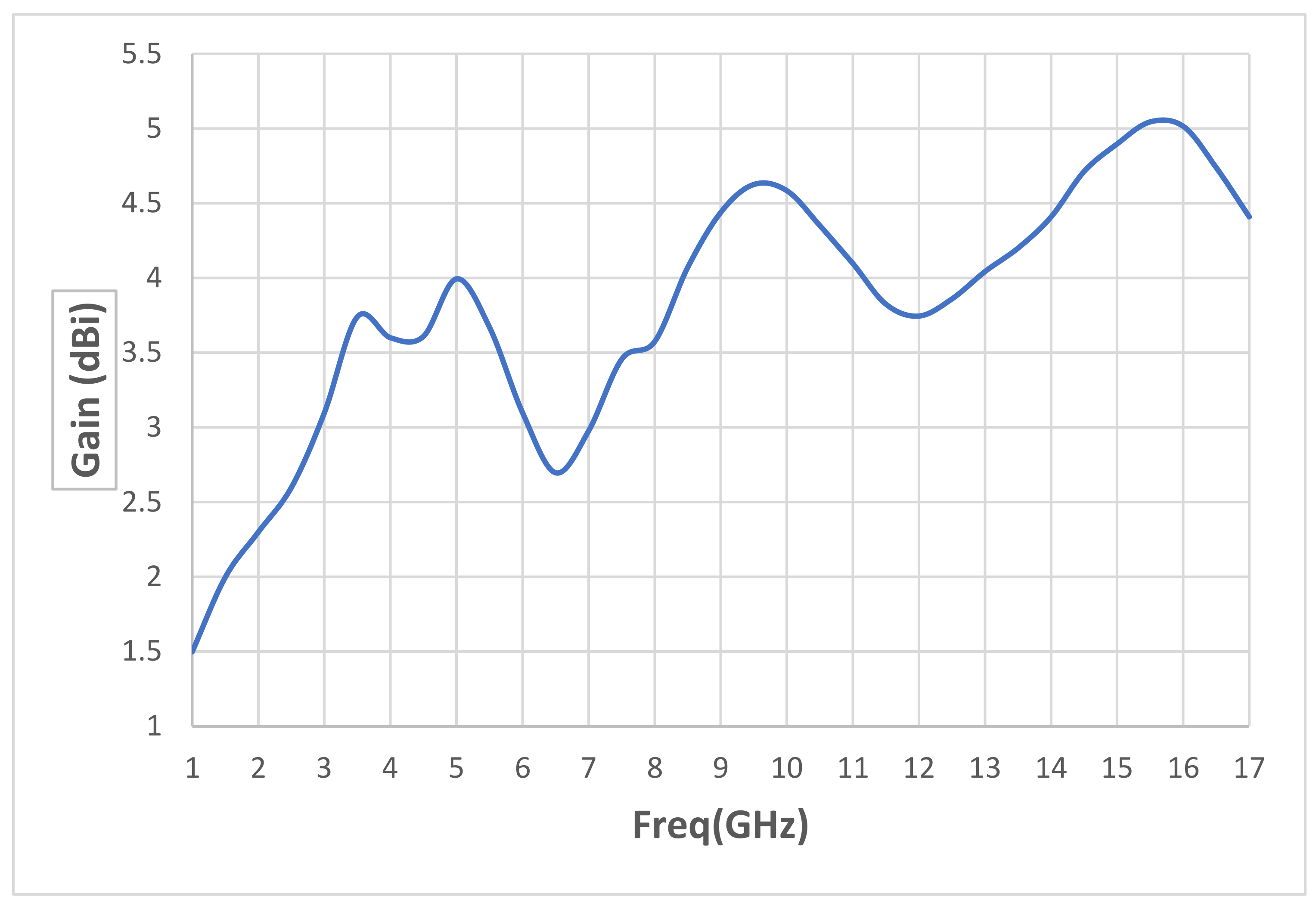
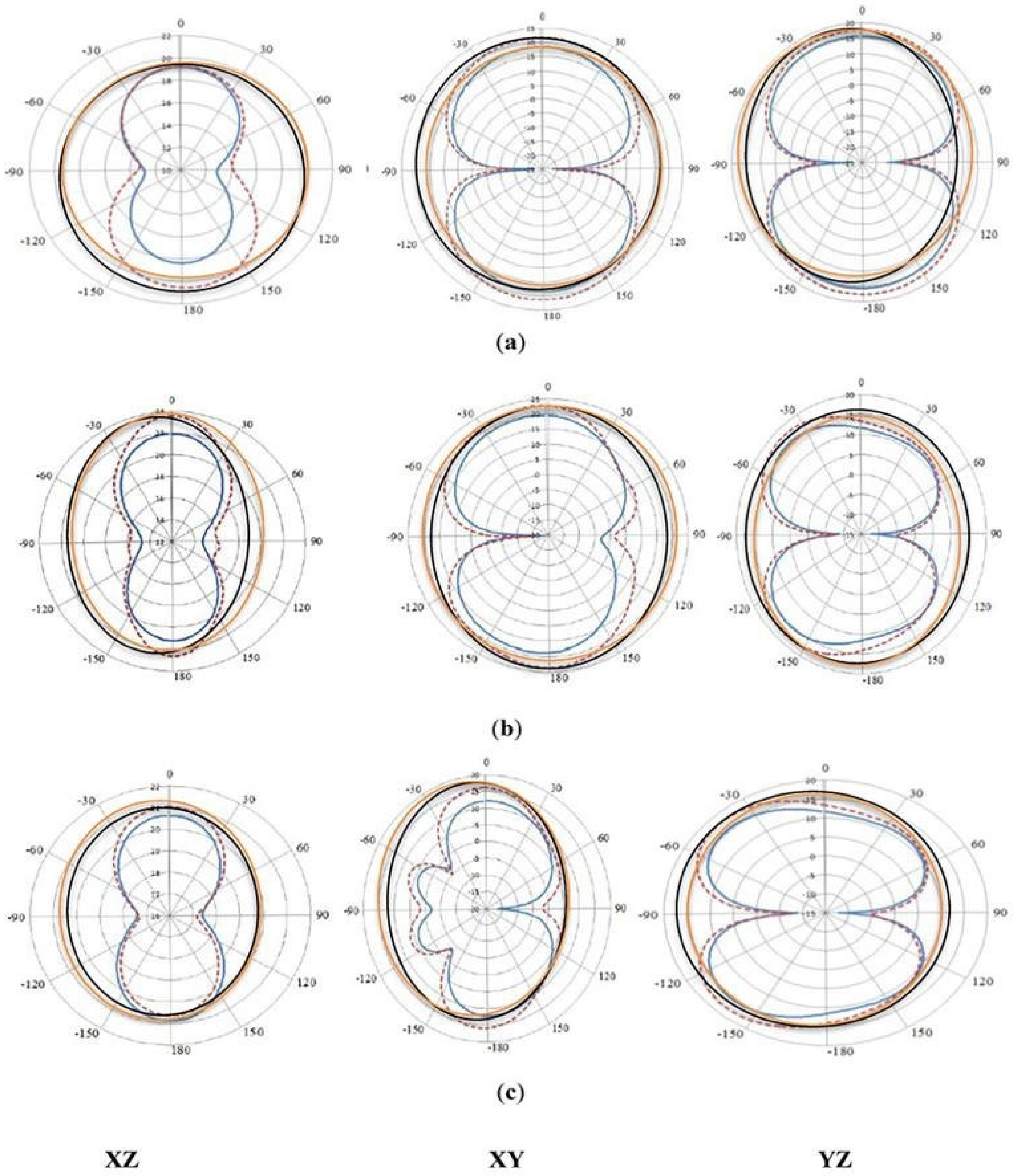
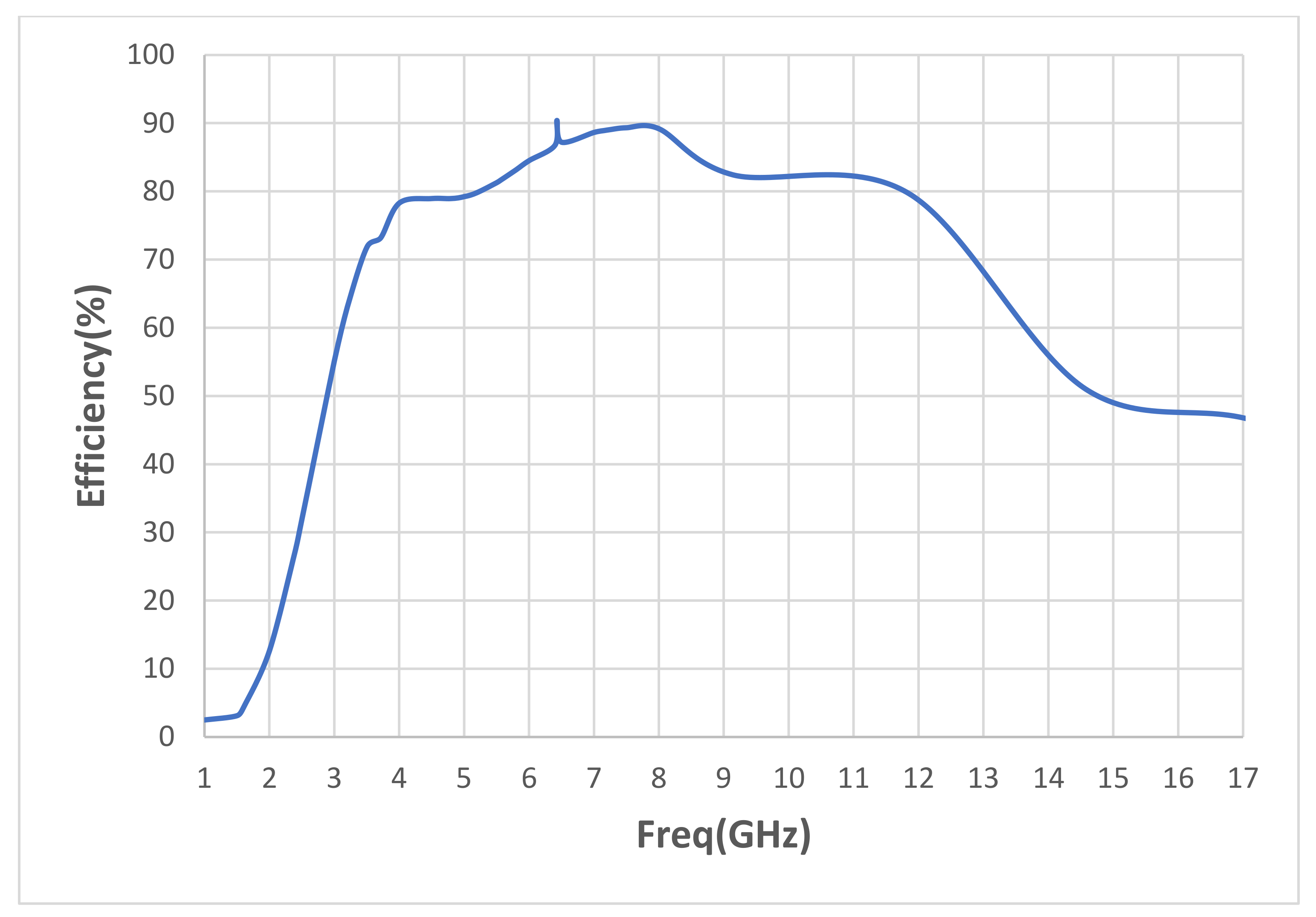
In Figure 10, the gain value for UWB is demonstrated within a frequency range of 1–17 GHz of the projected UWB antenna. In general, an antenna’s gain increases as its working frequency rises. As shown in Figure 10, this did not entirely occur, since efficiency determines the relationship between frequency and directivity, but not gain. Inadequate impedance matching between the feedline and the antenna, conductor loss, and dielectric loss are the primary causes of efficiency degradation. One of the criteria in determining losses appears to be changing. When the antenna’s wavelength is almost equal to or larger than the wavelength, side lobes do form, resulting in a loss of directivity. The far-field radiation pattern results for the projected antenna, for specified frequencies, have been simulated, as depicted in Figure 11, clarifying a polar plot of the radiation pattern in three planes: XZ (ø = 0°), XY (θ = 90°), and YZ (ø = 90°) at 3.581, 8, and 14 GHz. The proposed antenna has demonstrated sensible radiation pattern characteristics with mostly symmetrical behaviors at these frequencies. An antenna’s efficiency in transmitting and receiving radiofrequency (RF) signals can be measured in part by comparing the entire power radiated by the antenna to the whole power received from the generator. In practice, an antenna’s empty space is its only target when its radiation efficiency is at its highest. When radiation efficiency is low, most of the input power is lost due to losses in the antenna, such as metal conduction, dielectric, and magnetic losses. Figure 12 therefore illustrates the efficiency of radiation. Within the UWB frequency response, the maximum radiation efficiency was better than 82%.
This article compared the projected UWB antenna with the antennas demonstrated in [26,27,28,29,30,31,32,33,34,35,36,37,38,39,40]. Accordingly, the projected antenna in this article is, mostly, of minimum physical size and maximum bandwidth, with other competitive antenna parameters, as shown in Table 1.

5. Fabrication and Measurements

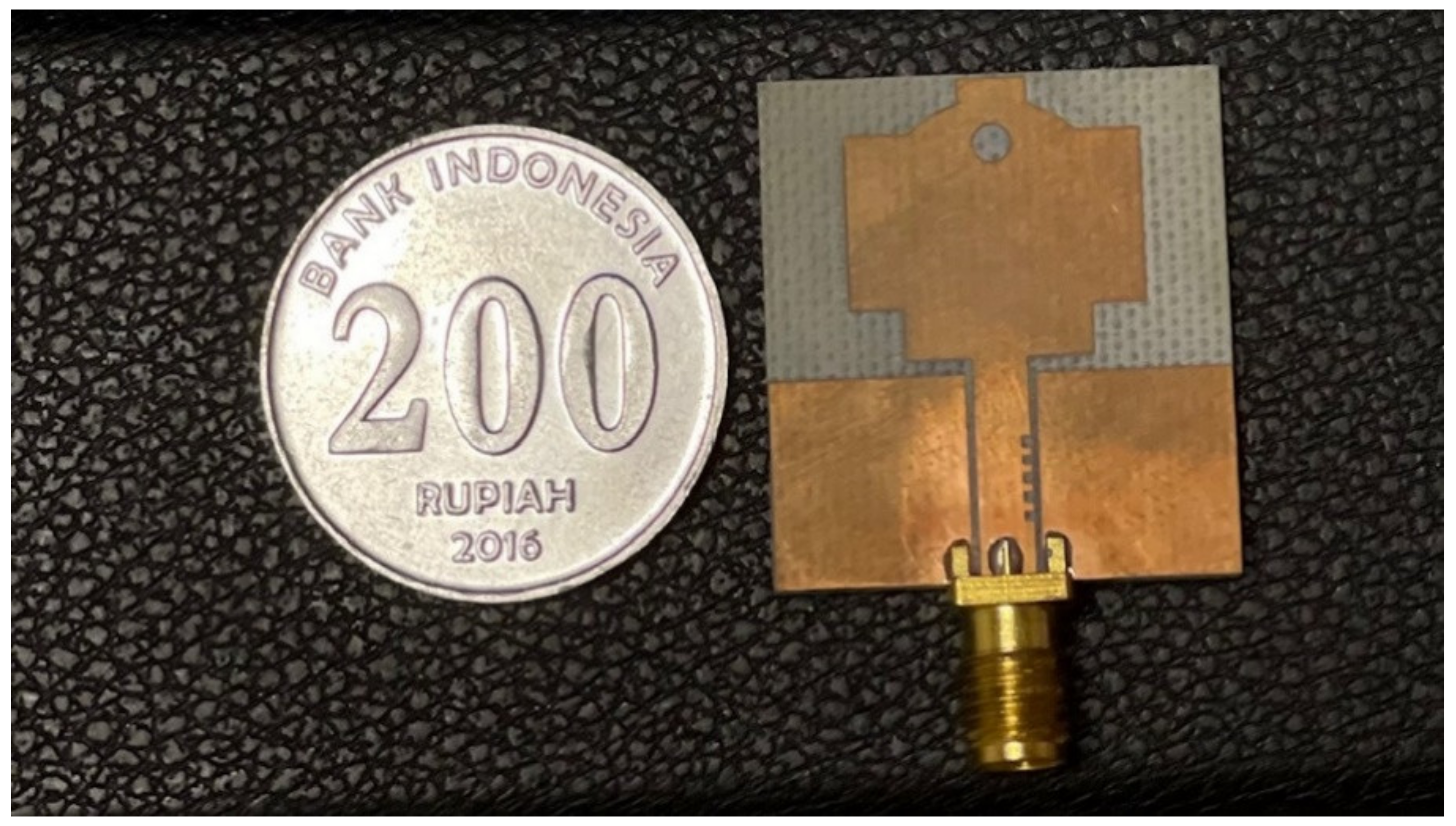
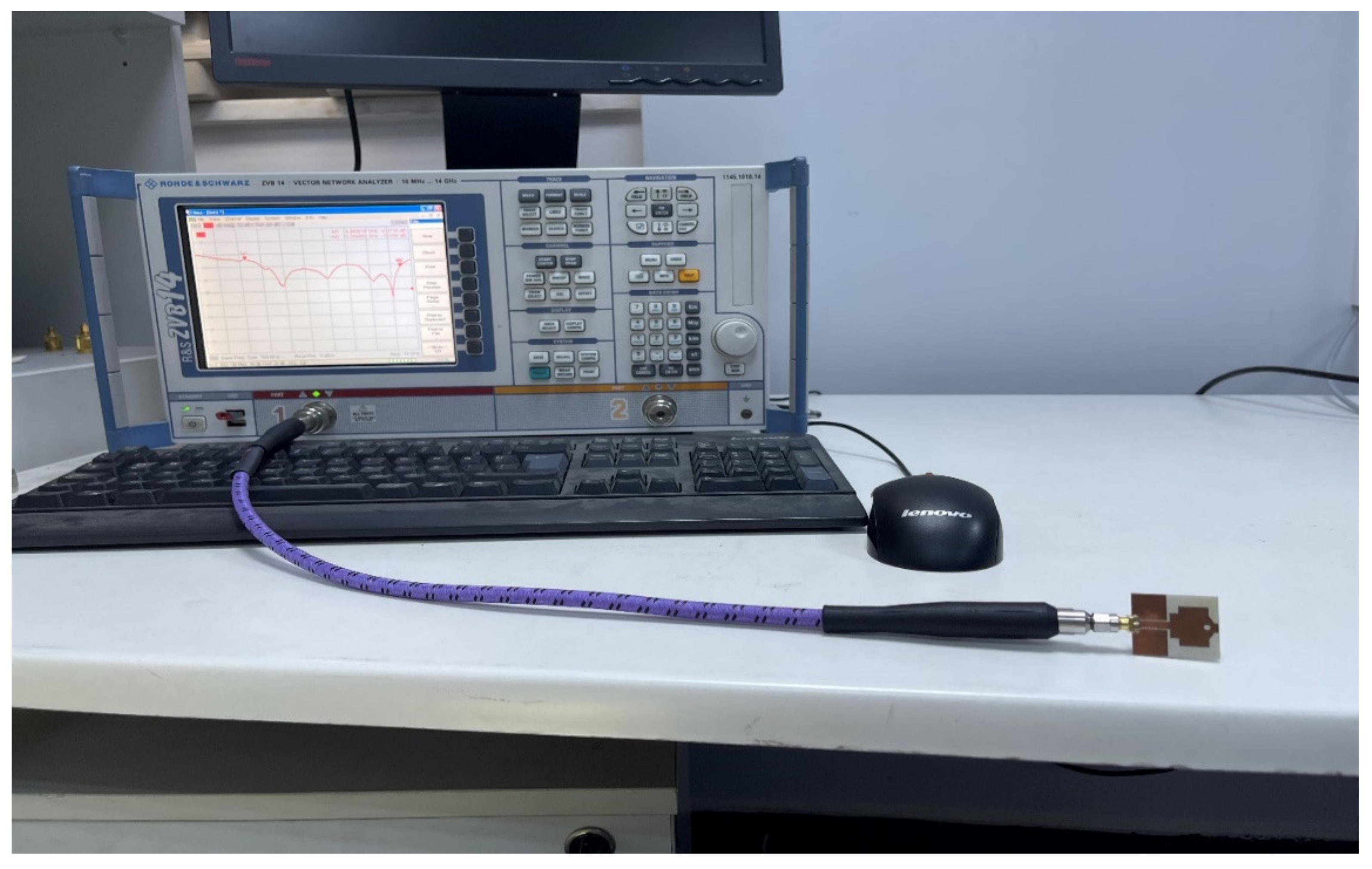
Using an LPKF ProtoMat S63, we produced the suggested UWB antenna prototype. To begin, a model was created on the FR4-epoxy substrate. An SMA coaxial connector was used to connect the feedline end, as shown in Figure 13. Then, the Rohde&Schwarz®ZVB14 Vector Network Analyzer has been employed to test our prototype as depicted at this point, as shown in Figure 14. Figure 15 shows agreeable simulation and measurement consequences for the projected CPW antenna’s input reflection. It is possible to discern differences between these results in the S11 response, including the minor variation in the UWB frequency range. SMA connector proficiency, soldering impact, assembly resistance, and dielectric substrate losses all play a role in these variances in S11 performance.

6. Rectifier Antenna (Rectenna)

One of the most promising new methods for utilizing the plentiful electromagnetic energy in the atmosphere to power low-power electronic devices is RF energy harvesting, often known as RF energy scavenging (e.g., TV and radio broadcastings, wireless LAN, and mobile phone signals). By obviating the need for batteries and other power supply resources, this is a fantastically valuable system design feature [41]. Solar radiation, heat, vibration, piezoelectric energy, thermal energy, and electromagnetic waves or radiofrequency are only some of the natural energy sources that can be harnessed and converted into usable DC power using the method’s wireless power transfer mechanism. Recent decades have seen a meteoric development in the usage of RF energy harvesting from the surrounding environment. This method of RF harvesting is the most significant because it is readily available and requires little effort to scavenge. Since thermal energy presupposes the presence of heat, it is uncontrollable by humans [42].
Several rectennas have been built and studied for RF energy harvesting. Rectenna performance can be judged in part by how well they convert RF energy to DC. In terms of conversion efficiency, monopole rectennas are among the best. However, these rectennas often work best with a single frequency band and demand a lot of power. If you want to take advantage of more of the RF energy in the environment, a multiband or broadband aerial array that can run on a little amount of power [39] is a practical option.
This investigation used a one-of-a-kind harvester antenna layout that is wirelessly connected to a two-stage rectifier circuit that features a reversed L-type matching impedance. The rectifier circuit uses a voltage doubler topology and has only two parts: a capacitor and a Schottky diode that can accept a Wi-Fi input signal at 2.45 GHz from a harvester antenna. Rectification is accomplished using a zero-biased Schottky diode in the SMS7630 model, and even a weak input signal of −10 dBm is sufficient to convert the RF input power into the DC output voltage. The results of the simulations revealed that impedance matching is necessary for a two-stage rectifier circuit to produce a higher DC output voltage with good power conversion efficiency, which is necessary for enabling low-power electronic devices [42]. In order to cover the UWB spectrum as well as other important bands, the new design optimizes the distance between the patch and the CPW ground (radio, GSM, and ISM). An increase in bandwidth and impedance matching for the UWB range was achieved by chamfering the corners, cutting two slots in the CPW ground, and employing dual-stubs. In the novel design, the desired band rejection is tuned by placing a parasitic patch above the aerial patch. The overall layout has been improved upon throughout its development. Small in volume (only 50401.6 mm3), the structure is easily transportable. The mobile, military, and satellite industries can all benefit from it [40]. Rectennas are described in [43], wherein a receiving aerial array and a rectifier optimized for low incident power conditions are combined to create a device that is independent of the orientation of the energy source. The method of designing the receiving array is based on quadratically constrained quadratic programming, which maximizes the efficiency with which power is sent. The receiving antenna features an adjustable angular coverage beam with a flat top, making it suitable for a variety of uses. The SMS 7630 diode was chosen and installed on the rectifier when the incident power was low in order to maximize the rectification efficiency. An array of six patch receivers separated by less than half a wavelength and a rectifier operating in the 5.8 GHz ISM band were constructed and tested to verify the design procedure. When the energy source was moved from −45 degrees to +45 degrees in the H-plane, the findings demonstrated that the value of the output dc voltage was almost unaffected. Focusing on the many methods accepted to achieve a compact rectenna, frequency, and polarization selectivity, the study in [44] analyzes the clarification and consultation of various map outsets from the perspectives of miniaturization, fated-tolerant, and harmonic rejections. It is helpful to increase the percentage of energy received using harvesting technologies. The number of energy harvesting antennas required to cover a certain area or region is high. An effective stepped impedance stub matching circuit was demonstrated for use in a dual-band rectifier [37]. Dual-band impedance matching circuits, which incorporate a stepped impedance stub, were theoretically investigated, and their results were incorporated into the design of the resulting dual-band rectifier. The proposed dual-band matching circuit can be evaluated and forecasted in terms of its frequency ratio utilizing simulation. For the purpose of demonstration, a dual-band rectifier has been constructed that can switch between 0.915 and 2.45 GHz and has dimensions of 21.47 mm by 18.93 mm. The results of the measurements show that at 0.915 GHz and 2.45 GHz, the rectifier achieved its maximum efficiency of 74% and 73%, with a load of 1500. Since the dual-band matching network in this research is so simply and effectively constructed, the dual-band rectifier is small and powerful.

Simulated and Measured Results of Antenna and Rectifier Circuit

With the CST simulator, we constructed and simulated a rectifier circuit, which rectifies the received signal via the antenna and then supplies power to the load. Boost or buck converters can also be used to boost or convert a low-voltage signal.
When the signal voltage is low, a boost or buck converter can be employed to increase it. This configuration is a full-wave bridge circuit because it produces voltage for both the positive and negative cycles of the wave, and it uses a voltage doubler as a rectifier circuit to convert the AC signal received from the antenna to DC output voltage. When we use two stubs to connect the antenna to the rectified input, we may cancel out any harmonic frequencies that might otherwise be present. To match 4.4 GHz and provide the best return loss, the length and width of both stubs were modified. With the right combination of components in the rectifier circuit and antenna, full power can be delivered in both directions. One strategy to improve the low-power performance of the multiplier circuit is to use stub element matching [45].
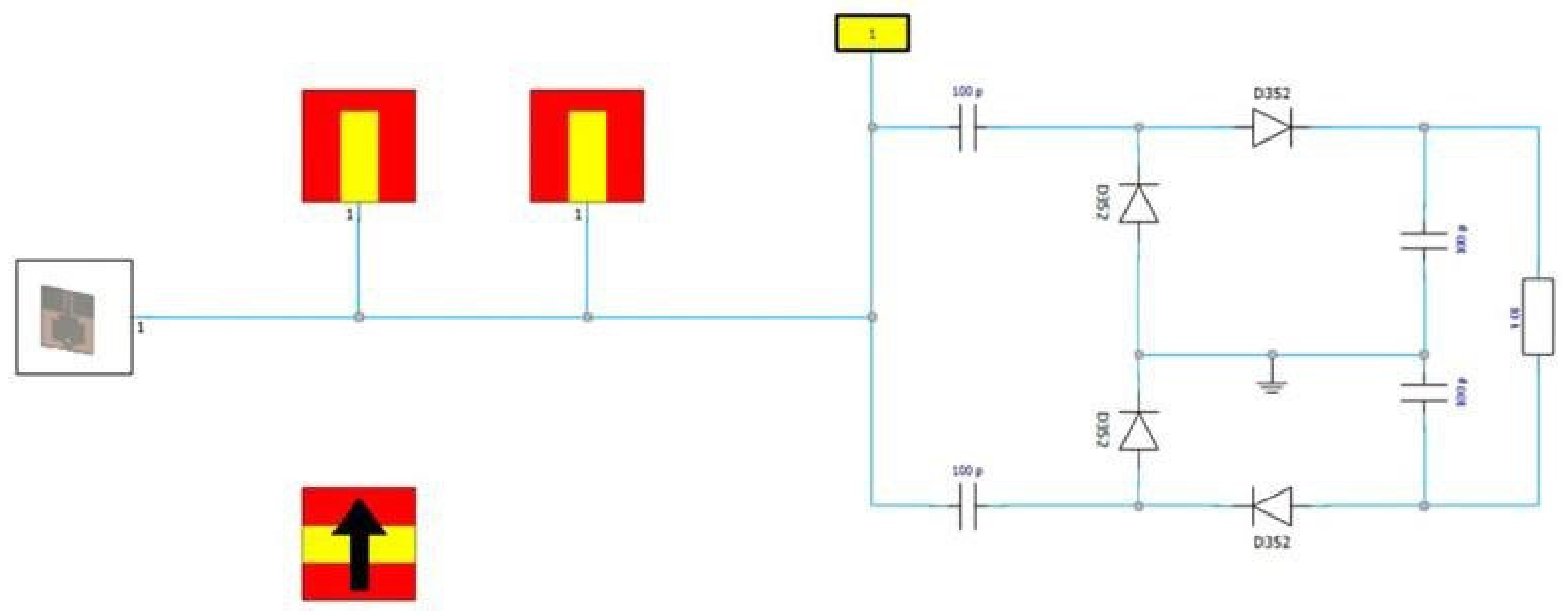
As LPF is more difficult to design, the stubs approach was chosen instead because it simplifies the circuit while simultaneously reducing its complexity. The completed CST MWS rectifier antenna simulation is depicted in Figure 16, while measured and simulated S11 responses are depicted in Figure 17. Both are depicted as a low-pass filters. To design a rectifier circuit, Schottky diodes are preferred over PN diodes due to their low-voltage threshold (low-voltage drop across the diode terminals) and reduced junction capacitance. The diode’s maximum frequency was raised thanks to its low threshold and low junction capacitance, both of which allow it to function more efficiently at low power levels. Due to its quick switching speed, the SMS 7630-005LF model of the standard Schottky diode was chosen. As the resistance “Rs” is in series with a variable junction resistance “Rj” in parallel with a variable junction capacitance “Cj,” impedance matching is made harder by the nonlinear nature of Schottky diodes in energy harvesting circuits. Accordingly, Schottky diodes were chosen due to their fast forward switching or low received power [46].
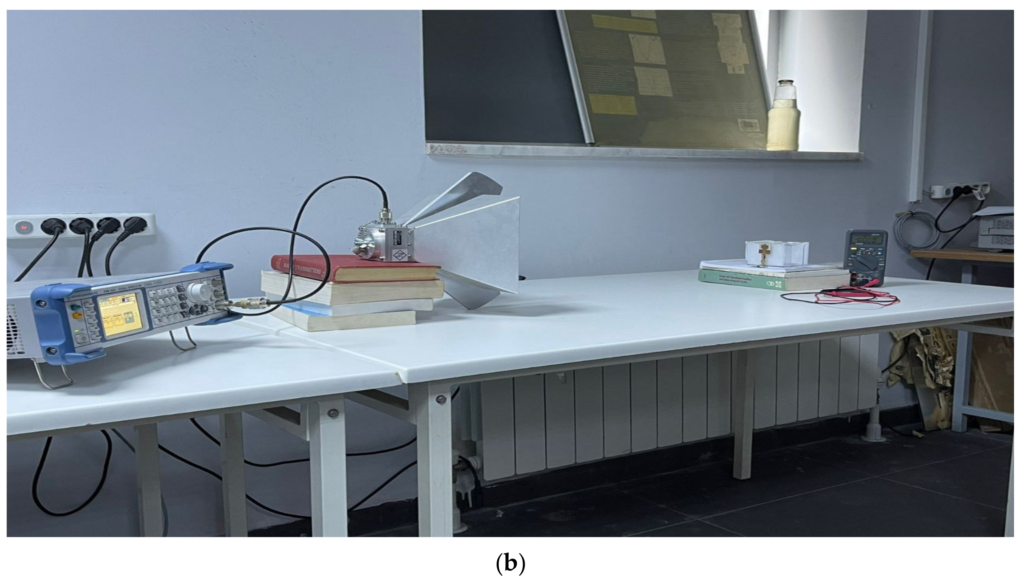
Low-power electronic gadgets and sensor networks will have a bright future thanks to RF energy harvesting technologies. Antenna Magus software was used to simulate the design using CST MWS and an ultra-wideband coplanar waveguide antenna to pick up radio waves around the 4.4 GHz region. This design relies on Antenna Magus software to make the design process easier. The antenna’s modest size is due to the use of a Schottky diode model, SMS 7630-005LF. The rectenna setup for measurements is depicted in Figure 18. Output DC voltage values are shown in Table 2. The highest and lowest dc voltages were 1.65 and 0.5 V, at −8 and −3 dBm transmitter powers.

7. Conclusions

In recent years, an increase in efforts has been seen to reduce the size and bandwidth of UWB antennas. The limited bandwidth of a microstrip antenna can be effectively resolved by inserting slots to a patch radiator or ground planes. To achieve the above goals, a new compact monopole antenna design using the FR4 substrate fed by CPW with various slot shapes in the radiating patch based on the Locked-Key topology has been presented. The simulated S11 scattering response specified the UWB bandwidth of 10.354 GHz with acceptable input reflection. The simulated S11 consequences were in good agreement with the measurements. Compared to several documented UWB-based antennas in the literature, the suggested antenna has more compactness and a higher bandwidth. The rectenna simulation model has been investigated using two stubs and the Schottky diode model SMS 7630-005LF. Output DC voltage has been measured for the projected rectenna around the 4.4 GHz region. The highest and lowest measured dc voltages were 1.65 and 0.5 V, at −8 and −3 dBm transmitter powers.

Author Contributions

Software, Y.S.M.; formal analysis, Y.S.M.; investigation, Y.S.M.; writing—original draft preparation, M.S.J.; writing—review and editing, Y.S.M.; supervision, D.C.A.; project administration, D.C.A. All authors have read and agreed to the published version of the manuscript.

Funding

This research received no external funding.

Data Availability Statement

The data presented in this study are available in miniaturized coplanar waveguide-fed UWB antenna for wireless applications.

Acknowledgments

Special thanks to research assistant “Sedat Kilinc” of Istanbul University, Cerrahpasa RF Lab, for his support with the measurements.

Conflicts of Interest

The authors declare no conflict of interest.

References

  1. Varum, T.; Caiado, J.; Matos, J. Compact Ultra-Wideband Series-Feed Microstrip Antenna Arrays for IoT Communications. Appl. Sci. 2021, 11, 6267. [Google Scholar] [CrossRef]
  2. Sediq, H.T.; Nourinia, J.; Ghobadi, C.; Mohammadi, B. A novel shaped ultrawideband fractal antenna for medical purposes. Biomed. Signal Process. Control. 2023, 80, 104363. [Google Scholar] [CrossRef]
  3. Abbas, A.; Hussain, N.; Jeong, M.-J.; Park, J.; Shin, K.S.; Kim, T.; Kim, N. A Rectangular Notch-Band UWB Antenna with Controllable Notched Bandwidth and Centre Frequency. Sensors 2020, 20, 777. [Google Scholar] [CrossRef] [PubMed] [Green Version]
  4. Wang, M.; Wang, H.; Chen, P.; Ding, T.; Xiao, J.; Zhang, L. A butterfly-like slot UWB antenna with WLAN band-notch characteristics for MIMO applications. IEICE Electron. Express 2022, 19, 20220233. [Google Scholar] [CrossRef]
  5. Saha, T.K.; Goodbody, C.; Karacolak, T.; Sekhar, P.K. A compact monopole antenna for ultra-wideband applications. Microw. Opt. Technol. Lett. 2019, 61, 182–186. [Google Scholar] [CrossRef] [Green Version]
  6. Soni, R.; Gupta, R.; Sen, D. Efficient Design of Micro Strip Patch Antenna for the Ultra-Wideband (UWB) Applications. Int. J. Recent Technol. Eng. (IJRTE) 2020, 8, 4517–4520. [Google Scholar] [CrossRef]
  7. Dwivedi, A.K.; Mishra, B.; Singh, V.; Tripathi, P.N.; Singh, A.K. Design of a Compact CPW-Fed Monopole Antenna With Asymmetrical Hexagonal Slot Loaded Ground Structure for C/X/Ku Band Applications. Electr. Control. Commun. Eng. 2020, 16, 15–22. [Google Scholar] [CrossRef]
  8. Venkatachalam, D.; Govindasamy, M. A CPW-Fed hexagonal antenna with fractal elements for UWB applications. Appl. Math. Inf. Sci. Int. J. 2019, 13, 73–79. [Google Scholar]
  9. Pandey, A.K.; Singh, R. CPW Fed Micro Strip Patch Antenna for Wireless Communication. Int. J. Eng. Adv. Technol. 2017, 6, 196–200. [Google Scholar]
  10. Awan, W.A.; Zaidi, A.; Hussain, N.; Iqbal, A.; Baghdad, A. Stub loaded, low profile UWB antenna with independently controllable notch-bands. Microw. Opt. Technol. Lett. 2019, 61, 2447–2454. [Google Scholar] [CrossRef]
  11. Al-Azzawi, A.A.; Al-Hilalli, A.; Al-Majdi, K.; Almukhtar, A.A.; Mezaal, Y.S. New miniature microstrip antenna for UWB wireless communications. Proc. Est. Acad. Sci. 2022, 71, 194. [Google Scholar] [CrossRef]
  12. Al-Gburi, A.J.A.; Ibrahim, I.; Zeain, M.Y.; Zakaria, Z. Compact Size and High Gain of CPW-fed UWB Strawberry Artistic shaped Printed Monopole Antennas using FSS Single Layer Reflector. IEEE Access 2020, 8, 92697–92707. [Google Scholar] [CrossRef]
  13. Aissaoui, D.; Chaabane, A.; Boualleg, A.; Guerroui, M. Coplanar Waveguide-fed UWB Slotted Antenna with Notched-band Performance. Period. Polytech. Electr. Eng. Comput. Sci. 2021, 65, 69–73. [Google Scholar] [CrossRef]
  14. Rahman, M.; NagshvarianJahromi, M.; Mirjavadi, S.S.; Hamouda, A.M. Compact UWB Band-Notched Antenna with Integrated Bluetooth for Personal Wireless Communication and UWB Applications. Electronics 2019, 8, 158. [Google Scholar] [CrossRef] [Green Version]
  15. Ahmad, S.; Ijaz, U.; Naseer, S.; Ghaffar, A.; Qasim, M.A.; Abrar, F.; Parchin, N.O.; See, C.H.; Abd-Alhameed, R. A Jug-Shaped CPW-Fed Ultra-Wideband Printed Monopole Antenna for Wireless Communications Networks. Appl. Sci. 2022, 12, 821. [Google Scholar] [CrossRef]
  16. Al-Gburi, A.J.A.; Ibrahim, I.M.; Zakaria, Z.; Abdulhameed, M.K.; Saeidi, T. Enhancing Gain for UWB Antennas Using FSS: A Systematic Review. Mathematics 2021, 9, 3301. [Google Scholar] [CrossRef]
  17. Yeboah-Akowuah, B.; Tchao, E.T.; Ur-Rehman, M.; Khan, M.M.; Ahmad, S. Study of a printed split-ring monopole for dual-spectrum communications. Heliyon 2021, 7, e07928. [Google Scholar] [CrossRef]
  18. Al-Gburi, A.J.A.; Ibrahim, I.B.M.; Zakaria, Z.; Ahmad, B.H.; Bin Shairi, N.A.; Zeain, M.Y. High Gain of UWB Planar Antenna Utilising FSS Reflector for UWB Applications. Comput. Mater. Contin. 2022, 70, 1419–1436. [Google Scholar] [CrossRef]
  19. Benkhadda, O.; Ahmad, S.; Saih, M.; Chaji, K.; Reha, A.; Ghaffar, A.; Khan, S.; Alibakhshikenari, M.; Limiti, E. Compact Broadband Antenna with Vicsek Fractal Slots for WLAN and WiMAX Applications. Appl. Sci. 2022, 12, 1142. [Google Scholar] [CrossRef]
  20. Anveshkumar, N.; Gandhi, A.S. A survey on microstrip antennas for portable wireless communication system applications. In Proceedings of the 2017 International Conference on Advances in Computing, Communications and Informatics (ICACCI), Udupi, India, 13–16 September 2017; pp. 2156–2165. [Google Scholar]
  21. Seker, C.; Güneşer, M.T. A single band antenna design for future millimeter wave wireless communication at 38 GHz. Eur. J. Eng. Form. Sci. 2018, 2, 34–38. [Google Scholar]
  22. Khanna, P.; Sharma, A.; Singh, A.K.; Kumar, A. A novel approach for production challenges of flexible microstrip patch antenna. Brill. Eng. 2019, 1, 7–12. [Google Scholar]
  23. Mondal, K. Bandwidth and gain enhancement of microstrip antenna by frequency selective surface for WLAN, WiMAX applications. Sadhana 2019, 44, 233. [Google Scholar] [CrossRef] [Green Version]
  24. Al-Ahmadi, A.; Khraisat, Y.S.H. Bandwidth Enhancement of Microstrip Patch Antenna. Appl. Phys. Res. 2019, 11, p35. [Google Scholar] [CrossRef] [Green Version]
  25. Tao, L.; Xu, J.; Li, H.; Hao, Y.; Huang, S.; Lei, M.; Bi, K. Bandwidth Enhancement of Microstrip Patch Antenna Using Complementary Rhombus Resonator. Wirel. Commun. Mob. Comput. 2018, 2018, 6352181. [Google Scholar] [CrossRef] [Green Version]
  26. Hamza, Q.M.; Nabil, S.M.; Hassan, M. Novel CPW-fed UWB antenna for X-band applications. Int. Symp. Adv. Electr. Commun. Technol. (ISAECT) 2019, 4, 78–82. [Google Scholar] [CrossRef]
  27. Sanmugasundaram, R.; Dileepan, D.; Natarajan, S. Design of CPW antenna for network applications. Int. J. Eng. Technol. 2018, 7, 2525–2527. [Google Scholar] [CrossRef]
  28. Sharma, A.; Khanna, P.; Shinghal, K.; Kumar, A. Design of CPW-Fed Antenna with Defected Substrate for Wideband Applications. J. Electr. Comput. Eng. 2016, 2016, 6546481. [Google Scholar] [CrossRef]
  29. Khanna, P.; Sharma, A.; Singh, A.K.; Kumar, A. A CPW—Fed octagonal ring-shaped wideband antenna for wireless applications. Adv. Electromagn. 2018, 7, 87–92. [Google Scholar] [CrossRef] [Green Version]
  30. Quddious, A.; Abbasi, M.A.B.; Antoniades, M.A.; Vryonides, P.; Fusco, V.; Nikolaou, S. Dynamically Reconfigurable UWB Antenna Using an FET Switch Powered by Wireless RF Harvested Energy. IEEE Trans. Antennas Propag. 2020, 68, 5872–5881. [Google Scholar] [CrossRef]
  31. Jansari, D.V.; Amineh, R.K. A two-element antenna array for compact portable MIMO-UWB communication systems. AIMS Electron. Electr. Eng. 2019, 3, 224–232. [Google Scholar] [CrossRef]
  32. Simorangkir, R.B.; Kiourti, A.; Esselle, K.P. UWB Wearable Antenna With a Full Ground Plane Based on PDMS-Embedded Conductive Fabric. IEEE Antennas Wirel. Propag. Lett. 2018, 17, 493–496. [Google Scholar] [CrossRef]
  33. Negi, D.; Khanna, R.; Kaur, J. Design and performance analysis of a conformal CPW fed wideband antenna with Mu-Negative metamaterial for wearable applications. Int. J. Microw. Wirel. Technol. 2019, 11, 806–820. [Google Scholar] [CrossRef]
  34. Rusdiyanto, D.; Apriono, C.; Astuti, D.W.; Muslim, M. Bandwidth and Gain Enhancement of Microstrip Antenna Using Defected Ground Structure and Horizontal Patch Gap. Sinergi 2021, 25, 153–158. [Google Scholar] [CrossRef]
  35. Lu, P.; Song, C.; Huang, K.M. Ultra-Wideband Rectenna Using Complementary Resonant Structure for Microwave Power Transmission and Energy Harvesting. IEEE Trans. Microw. Theory Tech. 2021, 69, 3452–3462. [Google Scholar] [CrossRef]
  36. Kumar, T.R.; Madhavan, M. Design and Optimization of Wearable Microstrip Patch Antenna using Hybrid Fuzzy Flamingo Swarm Optimization Algorithm for RF Energy Harvesting. Iran. J. Sci. Technol. Trans. Electr. Eng. 2022, 5, 1–20. [Google Scholar] [CrossRef]
  37. Imran, A.I.; Elwi, T.A.; Salim, A.J. On the Distortionless of Uwb Wearable Hilbert-Shaped Metamaterial Antenna for Low Energy Applications. Prog. Electromagn. Res. M 2021, 101, 219–239. [Google Scholar] [CrossRef]
  38. Kumar, M.; Kumar, S.; Jain, S.; Sharma, A. A Plug-in Type Integrated Rectenna Cell for Scalable RF Battery Using Wireless Energy Harvesting System. IEEE Microw. Wirel. Compon. Lett. 2022, 33, 98–101. [Google Scholar] [CrossRef]
  39. Shi, Y.; Jing, J.; Fan, Y.; Yang, L.; Wang, M. Design of a Novel Compact and Efficient Rectenna for Wifi Energy Harvesting. Prog. Electromagn. Res. C 2018, 83, 57–70. [Google Scholar] [CrossRef] [Green Version]
  40. Mathur, M.; Agrawal, A.; Singh, G.; Bhatnagar, S.K. A compact coplanar waveguide fed wideband monopole antenna for RF energy harvesting applications. Prog. Electromagn. Res. M 2018, 63, 175–184. [Google Scholar] [CrossRef] [Green Version]
  41. Koohestani, M.; Tissier, J.; Latrach, M. A miniaturized printed rectenna for wireless RF energy harvesting around 2.45 GHz. AEU—Int. J. Electron. Commun. 2020, 127, 153478. [Google Scholar] [CrossRef]
  42. Ismail, N.; Kadir, E.A. Reversed L-type Matching Impedance of RF-to-DC Rectifier for Energy Harvesting System. J. Electr. Electron. Syst. Res. 2021, 19, 167–172. [Google Scholar] [CrossRef]
  43. Cai, X.; Geyi, W.; Guo, Y. A Compact Rectenna With Flat-Top Angular Coverage for RF Energy Harvesting. IEEE Antennas Wirel. Propag. Lett. 2021, 20, 1307–1311. [Google Scholar] [CrossRef]
  44. Yadav, K.; Chaturvedi, A.; Sharma, G.K. Comparative Study of Antenna in RF -Energy Harvesting. In Proceedings of the 2022 2nd International Conference on Power Electronics & IoT Applications in Renewable Energy and its Control (PARC), Mathura, India, 21–22 January 2022; pp. 1–7. [Google Scholar] [CrossRef]
  45. Adami, S.E.; Zhu, D.; Li, Y.; Mellios, E.; Stark, B.H.; Beeby, S. A 2.45 GHz rectenna screen-printed on polycotton for on-body RF power transfer and harvesting. In Proceedings of the 2015 IEEE Wireless Power Transfer Conference (WPTC), Boulder, CO, USA, 13–15 May 2015; pp. 1–4. [Google Scholar]
  46. Valenta, C.R.; Durgin, G.D. Harvesting Wireless Power. IEEE Microw. Mag. 2014, 15, 108–120. [Google Scholar]
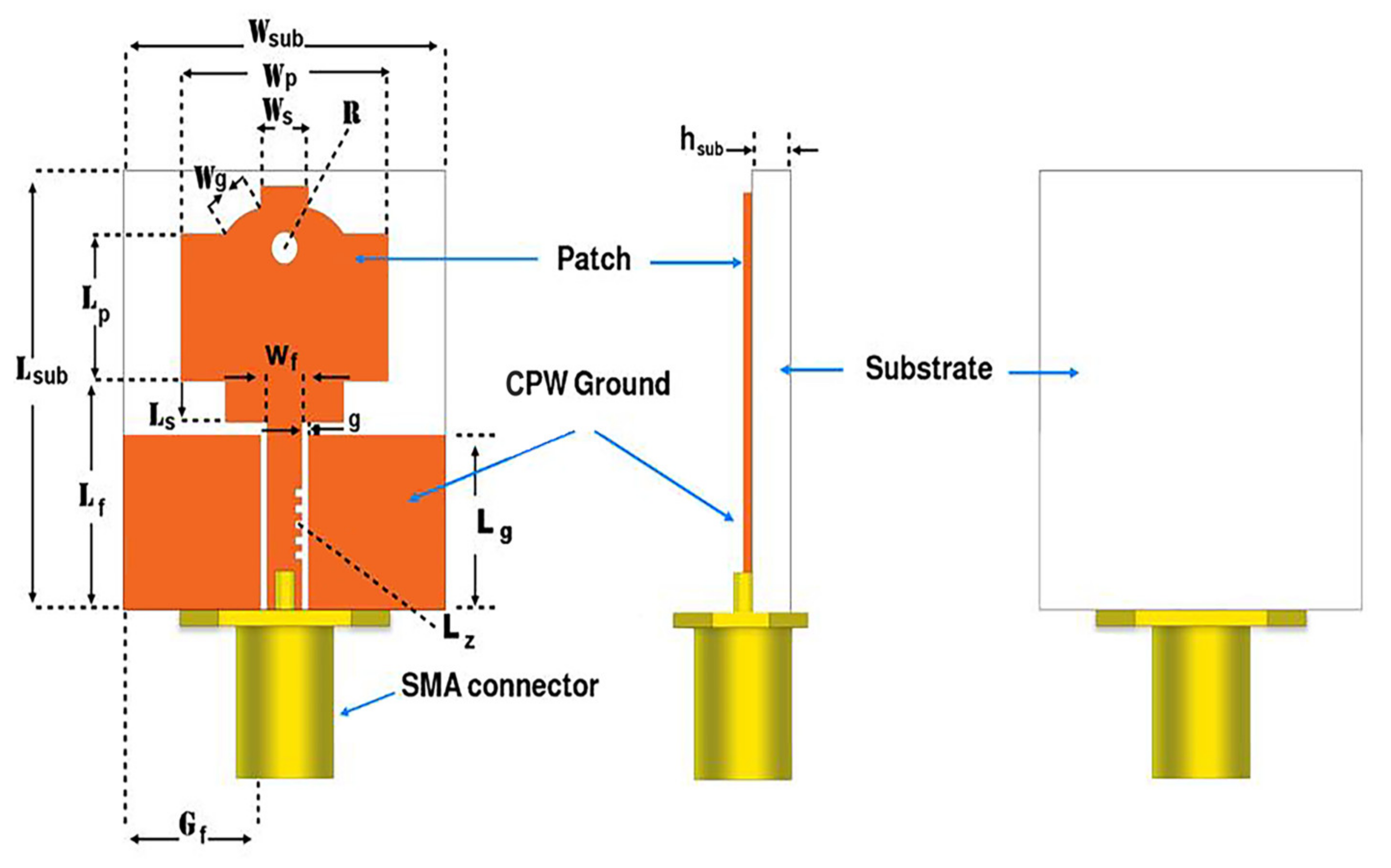
Figure 1. The topology of the projected CPW antenna based on the Locked-Key topology. Lsub = 27, Wsub = 25, R = 2, Wg = 2.94, Lp = 9.3, Lf = 14, Ls = 2.59, Ws = 3.8, Wf = 3, g = 0.35, Lg = 11, Lz = 0.5, Gf = 10.65, Wp = 16, hsub =1.5 (all dimensions in mm).
Symmetry 15 00633 g001
Figure 2. Procedural steps for design and optimizing of S11 responses of the UWB-CPW antenna.
Symmetry 15 00633 g002
Figure 3. The four steps for investigating various cases of the CPW-fed antenna design.
Symmetry 15 00633 g003
Figure 4. S11 response for each step of the projected CPW-fed antenna design.
Symmetry 15 00633 g004
Figure 5. (a) The circuit equivalent of the projected antenna and (b) its input reflection response. R1 = 2000 Ω, R2 = 10,000 Ω, R3 = 10,000 Ω, L1 = 5 nH, L2 = 40 nH, L3 = 0.6 nH, C1 = 1.1 pF, C2 = 0.01 pF, C3 = 0.1 pF.
Symmetry 15 00633 g005
Figure 6. Input reflection for the anticipated UWB antenna.
Symmetry 15 00633 g006
Figure 7. 3D radiation pattern at 8 GHz.
Symmetry 15 00633 g007
Figure 8. 3D radiation pattern at 12.2 GHz.
Symmetry 15 00633 g008
Figure 9. Surface current intensity distribution at (a) 3.57 GHz, (b) 8.76 GHz, and (c) 14 GHz.
Symmetry 15 00633 g009
Figure 10. The gain of the projected antenna within the 1–17 GHz frequency range.
Symmetry 15 00633 g010
Figure 11. 2D radiation patterns of the projected antenna at (a) 3.581, (b) 8 GHz, and (c) 14 GHz.
Symmetry 15 00633 g011
Figure 12. Radiation efficiency of the projected antenna.
Symmetry 15 00633 g012
Figure 13. The fabricated CPW-fed antenna prototype.
Symmetry 15 00633 g013
Figure 14. Antenna measurement setup.
Symmetry 15 00633 g014
Figure 15. Simulated and measured input reflection responses for the projected CPW-fed antenna.
Symmetry 15 00633 g015
Figure 16. The simulation model for the rectifier antenna (rectenna) circuit.
Symmetry 15 00633 g016
Figure 17. The simulated and measured S11 responses of the rectenna.
Symmetry 15 00633 g017
Figure 18. Rectenna setup: (a) UWB antenna with rectifier and (b) rectenna measurements.
Symmetry 15 00633 g018aSymmetry 15 00633 g018b
Table 1. The presented UWB antenna in this study as compared with reported UWB antennas.
Ref.Max. Efficiency (%)Max. Gain (dBi) within the BandDielectric ConstantSize
(mm3)
λ g 2   at   the   Lower   Frequency   Band Bandwidth Range
(GHz)
Applications
[26]833.18, 3.934.330 × 35 × 1.61.5149177–9.9UWB applications (X-band)
[27]---5.54.459.5 × 30 × 1.61.8326155.85–6.6Industrial Scientific and Medical Band applications.
[28]886.084.436 × 42 × 1.60.918544.5–13.5C and X band applications
[29]--3.54.447 × 47 × 1.60.265082–9.5S and C band applications
[30]40--2.227 × 33 × 0.7870.142563–11 (with 5 notches)UWB radiofrequency identification (RFID) is used for indoor localization
[31]---44.444 × 27 × 0.80.34253.1–10.6UWB multiple-input and multiple-output (MIMO) applications
[32]274.354.480 × 67 × 0.13 2.2013523.7–10.3 Wearable antenna applications
[33]8584.450 × 44.4 × 0.153.4525447.2–9.2 Wearable antenna applications
[34]----4.82.650 × 55 × 1.60.235672.07–2.83Application of wideband and multiband frequency
[35]73.43.72.2100 × 50 × 0.780.0568890.8–3.7Energy harvesting
[36]5832.2575.5 × 63.5 × 1.63.2210046.1–7.7Energy harvesting
[37]604.553.532 × 28 × 2.50.0143360.8–10Low-Energy Applications
[38]44.55.44.430 × 34.5 × 1.560.776255–6Scalable RF Battery
[39]5234.438 × 38 × 1.60.2608782.454–2.45Wi-Fi Energy Harvesting
[40]8774.450 × 40 × 1.60.0486900 MHz–3 GHz
5.6 GHz–9.9 GHz
RF Energy Harvesting Applications
Proposed824.74.427 × 25 × 1.50.2596773.581–13.935Energy harvesting
Table 2. Transmitter power and DC output voltage.
Transmitter Power (dBm)Rectifier O/P Voltage (mv)
01.17
−11.14
−20.84
−30.50
−41.59
−50.89
−60.81
−71.19
−81.65
−91.48
−101.1
Disclaimer/Publisher’s Note: The statements, opinions and data contained in all publications are solely those of the individual author(s) and contributor(s) and not of MDPI and/or the editor(s). MDPI and/or the editor(s) disclaim responsibility for any injury to people or property resulting from any ideas, methods, instructions or products referred to in the content.