
Scanning Probe Microscopy Investigation of Topological Defects

Abstract
:1. Introduction
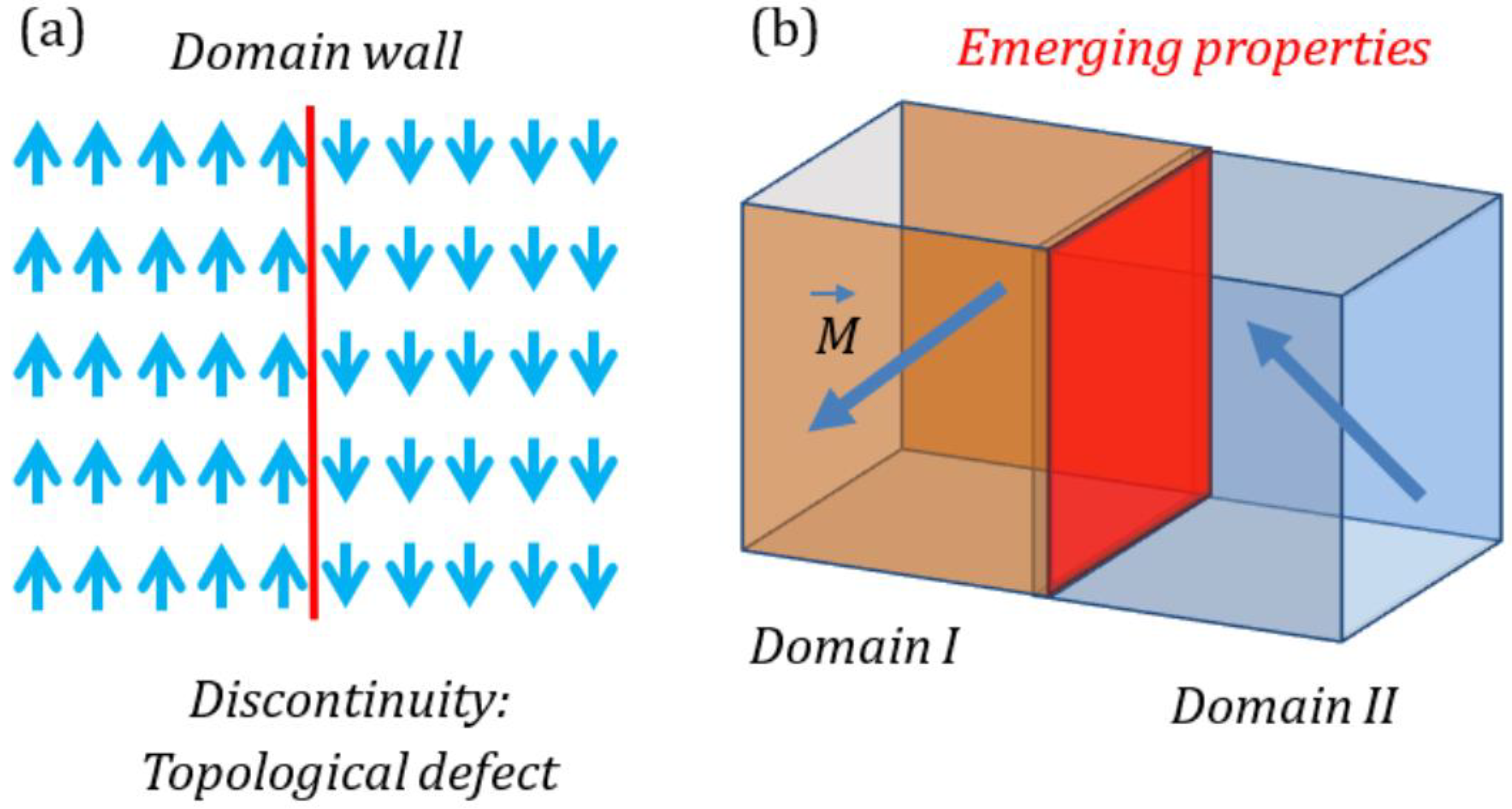
2. Types of Topological Defects
3. Scanning Probe Methods
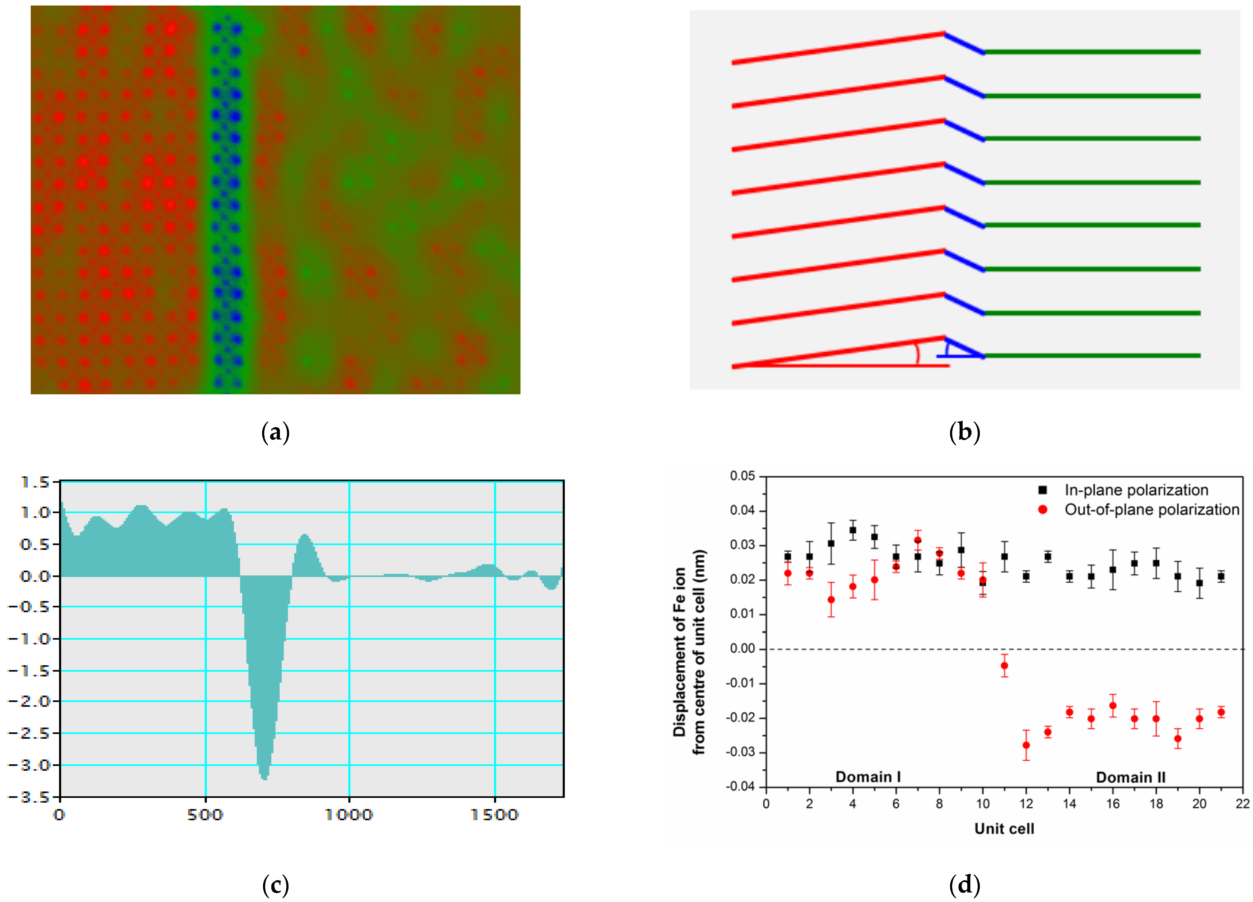
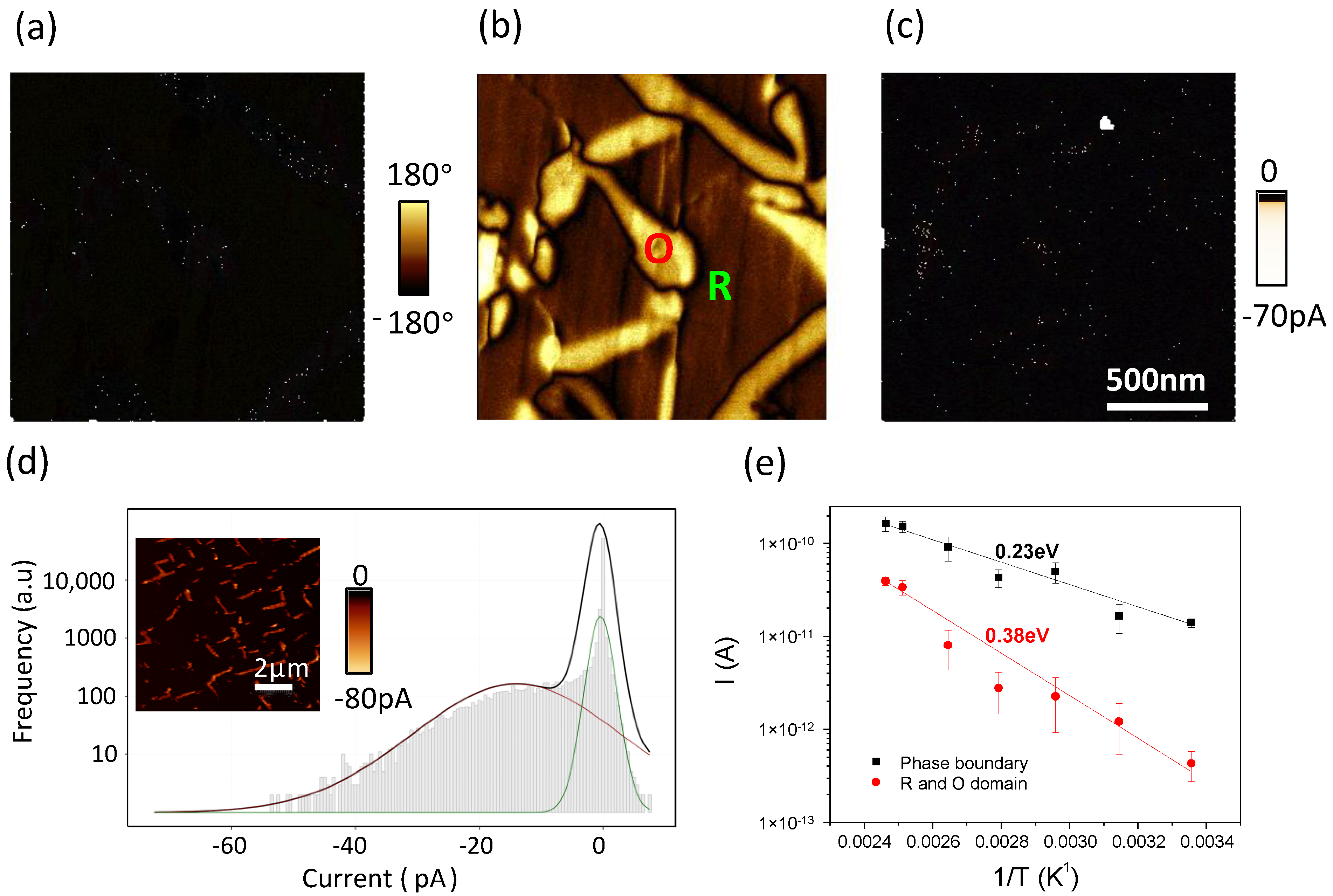
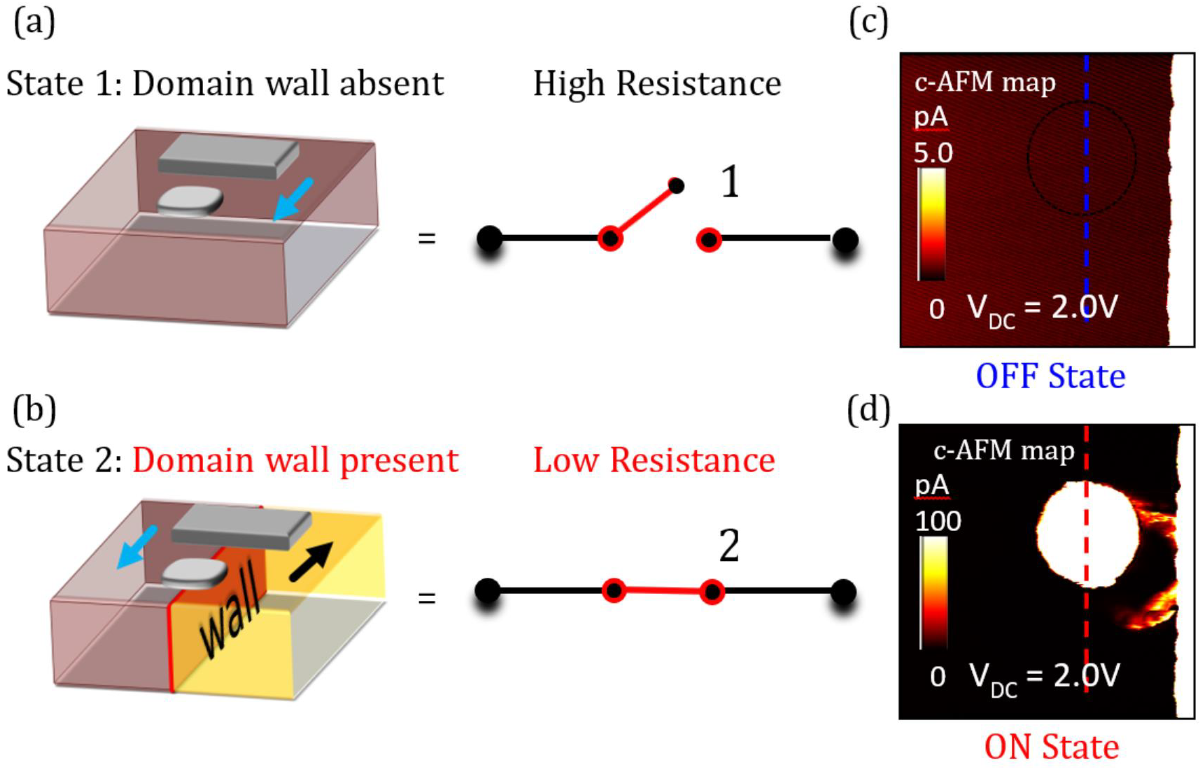
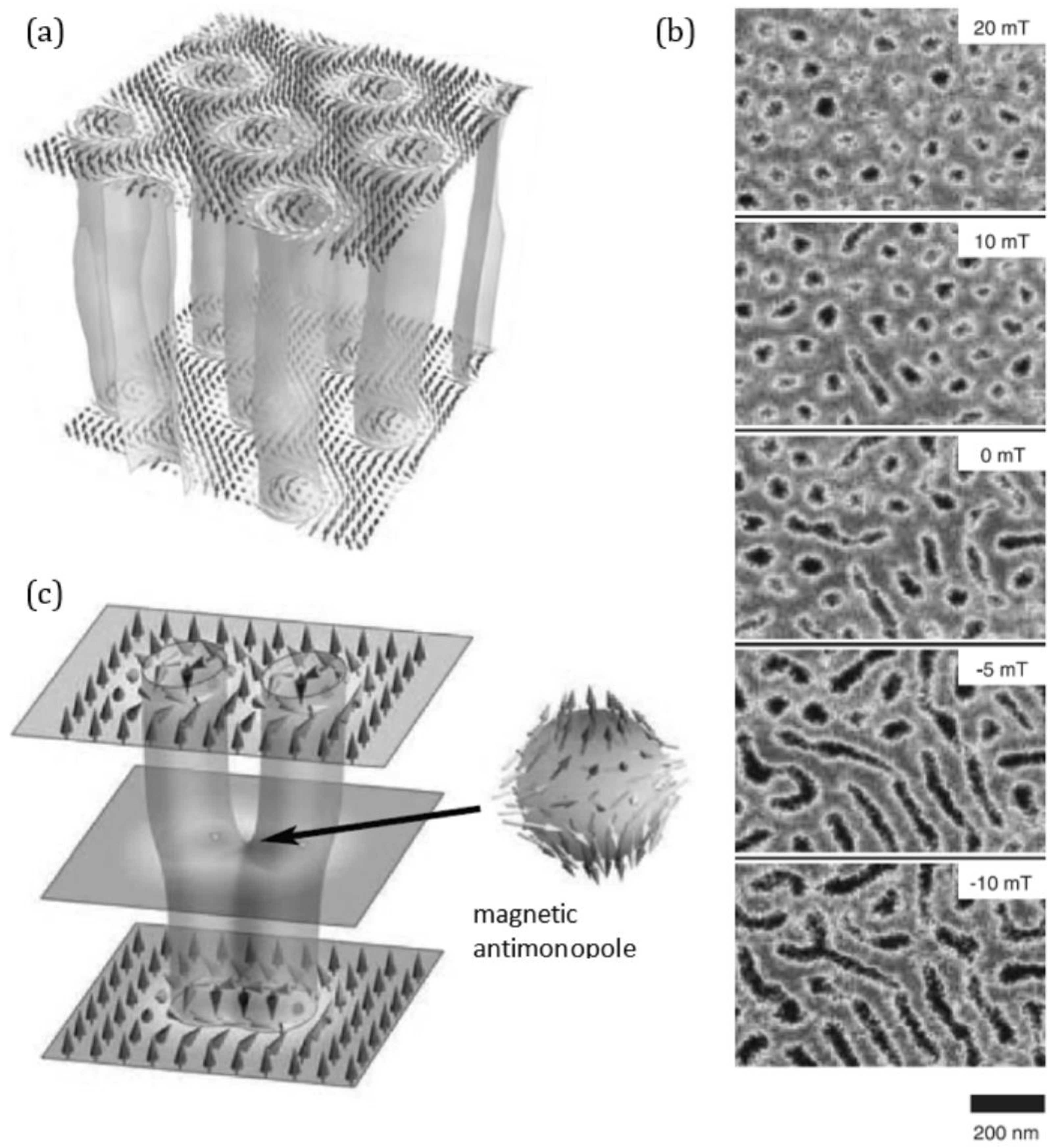
Application to Imaging and Manipulating Topological Defects
4. Concluding Remarks and Outlook
Funding
Institutional Review Board Statement
Informed Consent Statement
Data Availability Statement
Conflicts of Interest
References
- Mermin, N.D. The topological theory of defects in ordered media. Rev. Mod. Phys. 1979, 51, 591. [Google Scholar] [CrossRef]
- Přívratská, J.; Janovec, V. Pyromagnetic domain walls connecting antiferromagnetic non-ferroelastic magnetoelectric domains. Ferroelectrics 1997, 204, 321. [Google Scholar] [CrossRef]
- Přívratská, J.; Janovec, V. Spontaneous polarization and/or magnetization in non-ferroelastic domain walls: Symmetry predictions. Ferroelectrics 1999, 222, 23. [Google Scholar] [CrossRef]
- Catalan, G.; Seidel, J.; Ramesh, R.; Scott, J.F. Domain wall nanoelectronics. Rev. Mod. Phys. 2012, 84, 119. [Google Scholar] [CrossRef] [Green Version]
- Parkin, S.S.P.; Hayashi, M.; Thomas, L. Magnetic Domain-Wall Racetrack Memory. Science 2008, 320, 190–194. [Google Scholar] [CrossRef]
- Seidel, J. (Ed.) Topological Structures in Ferroic Materials: Domain Walls, Vortices and Skyrmions; Springer: Berlin, Germany, 2016; ISBN 978-3-319-25299-5. [Google Scholar] [CrossRef]
- Seidel, J.; Vasudevan, R.K.; Nagarajan, V. Topological structures in multiferroics: Domain walls, skyrmions and vortices. Adv. Electron. Mater. 2016, 2, 1500292. [Google Scholar] [CrossRef]
- Muhlbauer, S.; Binz, B.; Jonietz, F.; Pfleiderer, C.; Rosch, A.; Neubauer, A.; Georgii, R.; Boni, P. Skyrmion Lattice in a Chiral Magnet. Science 2009, 323, 915. [Google Scholar] [CrossRef] [Green Version]
- Yu, X.Z.; Onose, Y.; Kanazawa, N.; Park, J.H.; Han, J.H.; Matsui, Y.; Nagaosa, N.; Tokura, Y. Real-space observation of a two-dimensional skyrmion crystal. Nature 2010, 465, 901. [Google Scholar] [CrossRef]
- Balke, N.; Winchester, B.; Ren, W.; Chu, Y.H.; Morozovska, A.N.; Eliseev, E.A.; Huijben, M.; Vasudevan, R.K.; Maksymovych, P.; Britson, J.; et al. Enhanced electric conductivity at ferroelectric vortex cores in BiFeO3. Nat. Phys. 2012, 8, 81–88. [Google Scholar] [CrossRef]
- Göbel, B.; Mertig, I.; Tretiakov, O.A. Beyond skyrmions: Review and perspectives of alternative magnetic quasiparticles. Phys. Rep. 2021, 895, 1. [Google Scholar] [CrossRef]
- Bert, V. Atomic Force Microscopy. In NanoScience and Technology; Springer: Berlin, Germany, 2019. [Google Scholar]
- Giessibl, F.J. Advances in atomic force microscopy. Rev. Mod. Phys. 2003, 75, 949. [Google Scholar] [CrossRef] [Green Version]
- Kalinin, S.V.; Rodriguez, B.J.; Kholkin, A.L. Piezoresponse Force Microscopy and Spectroscopy. In Encyclopedia of Nanotechnology, Bhushan, B., Ed.; Springer: Dordrecht, Netherlands, 2012. [Google Scholar] [CrossRef]
- Gruverman, A.; Alexe, M.; Meier, D. Piezoresponse force microscopy and nanoferroic phenomena. Nat. Commun. 2019, 10, 1661. [Google Scholar] [CrossRef] [PubMed] [Green Version]
- Romming, N.; Hanneken, C.; Menzel, M.; Bickel, J.E.; von Bergmannn, B.W.K.; Kubetzka, A.; Wiesendanger, R. Writing and Deleting Single Magnetic Skyrmions. Science 2013, 341, 636. [Google Scholar] [CrossRef] [PubMed] [Green Version]
- Chiu, Y.-P.; Chen, Y.-T.; Huang, B.-C.; Shih, M.-C.; Yang, J.-C.; He, Q.; Liang, C.-W.; Seidel, J.; Chen, Y.-C.; Ramesh, R.; et al. Atomic-scale evolution of local electronic structure across multiferroic domain walls. Adv. Mater. 2011, 23, 1530. [Google Scholar] [CrossRef] [PubMed]
- Turner, P.W.; McConville, J.P.V.; McCaftan, S.J.; Campbell, M.H.; Schaab, J.; McQuaid, R.G.P.; Kumar, A.; Gregg, J.M. Large Carrier Mobilities in ErMnO3 Conducting Domain Walls Revealed by Quantitative Hall-Effect Measurements. Nano Lett. 2018, 18, 6381. [Google Scholar] [CrossRef] [PubMed] [Green Version]
- Seidel, J.; Martin, L.W.; He, Q.; Zhan, Q.; Chu, Y.H.; Rother, A.; Hawkridge, M.; Maksymovych, P.; Kalinin, S.; Gemming, S.; et al. Conduction at domain walls in oxide multiferroics. Nat. Mater. 2009, 8, 229. [Google Scholar] [CrossRef] [Green Version]
- Meier, D.; Seidel, J.; Cano, A.; Delaney, K.; Kumagai, Y.; Mostovoy, M.; Spaldin, N.A.; Ramesh, R.; Fiebig, M. Anisotropic conductance at improper ferroelectric domain walls. Nat. Mater. 2012, 11, 284. [Google Scholar] [CrossRef] [Green Version]
- Moore, S.L.; Ciccarino, C.J.; Halbertal, D.; McGilly, L.J.; Finney, N.R.; Yao, K.; Shao, Y.; Ni, G.; Sternbach, A.; Telford, E.J. Nanoscale lattice dynamics in hexagonal boron nitride moire superlattices. Nat. Commun. 2021, 12, 5741. [Google Scholar] [CrossRef]
- Eng, L.M.; Guntherodt, H.J. Scanning force microscopy and near-field scanning optical microscopy of ferroelectric and ferroelastic domain walls. Ferroelectrics 2000, 236, 35. [Google Scholar] [CrossRef]
- Seidel, J.; Eng, L.M. Shedding light on nanoscale ferroelectrics. Curr. Appl. Phys. 2014, 14, 1083. [Google Scholar] [CrossRef]
- Milde, P.; Köhler, D.; Seidel, J.; Eng, L.M.; Bauer, A.; Chacon, A.; Kindervater, J.; Mühlbauer, S.; Pfleiderer, C.; Buhrandt, S.; et al. Unwinding of a skyrmion lattice by magnetic monopoles. Science 2013, 340, 1076. [Google Scholar] [CrossRef] [PubMed]
- Kézsmárki, I.; Bordács, S.; Milde, P.; Neuber, E.; Eng, L.M.; White, J.S.; Rønnow, H.M.; Dewhurst, C.D.; Mochizuki, M.; Yanai, K.; et al. Néel-type skyrmion lattice with confined orientation in the polar magnetic semiconductor GaV4S8. Nat. Mater. 2015, 14, 1116. [Google Scholar] [CrossRef] [PubMed] [Green Version]
- Persky, E.; Kalisky, B. Scanning SQUID view of oxide interfaces. Adv. Mater. 2018, 30, 1706653. [Google Scholar] [CrossRef] [PubMed]
- Gross, I.; Akhtar, W.; Garcia, V.; Martinez, L.J.; Chouaieb, S.; Garcia, K.; Carretero, C.; Barthelemy, A.; Appel, P.; Maletinsky, P.; et al. Real-space imaging of non-collinear antiferromagnetic order with a single-spin magnetometer. Nature 2017, 549, 252. [Google Scholar] [CrossRef]
- Rondin, L.; Tetienne, J.-P.; Hingant, T.; Roch, J.-F.; Maletinsky, P.; Jacques, V. Magnetometry with nitrogen-vacancy defects in diamond. Rep. Prog. Phys. 2014, 77, 056503. [Google Scholar] [CrossRef] [Green Version]
- Tselev, A.; Meunier, V.; Strelcov, E.; Shelton, W.A.; Luk’yanchuk, I.; Jones, K.; Proksch, R.; Kolmakov, A.; Kalinin, S.V. Mesoscopic Metal-Insulator Transition at Ferroelastic Domain Walls in VO2. ACS Nano 2010, 4, 4412. [Google Scholar] [CrossRef]
- Ma, E.Y.; Cui, Y.-T.; Ueda, K.; Tang, S.; Chen, K.; Tamura, N.; Wu, P.M.; Fujioka, J.; Tokura, Y.; Shen, Z.-X. Mobile metallic domain walls in an all-in-all-out magnetic insulator. Science 2015, 350, 538. [Google Scholar] [CrossRef] [Green Version]
- Hong, S.; Tong, S.; Park, W.I.; Hiranaga, Y.; Cho, Y.; Roelofs, A. Charge gradient microscopy. Proc. Natl. Acad. Sci. USA 2014, 111, 6566. [Google Scholar] [CrossRef] [Green Version]
- Esfahani, E.N.; Liu, X.; Li, J. Imaging ferroelectric domains via charge gradient microscopy enhanced by principal component analysis. J. Mater. 2017, 3, 280. [Google Scholar] [CrossRef]
- Salje, E.K.H. Phase Transitions in Ferroelastic and Co-Elastic Crystals; Cambridge University Press: Cambridge, UK, 1990. [Google Scholar]
- Heo, Y.; Sharma, P.; Liu, Y.; Li, J.; Seidel, J. Mechanical probing of ferroelectrics at the nanoscale. J. Mater. Chem. C 2019, 7, 12441. [Google Scholar] [CrossRef]
- Heo, Y.; Lee, J.H.; Xie, L.; Pan, X.; Yang, C.-H.; Seidel, J. Enhanced conductivity at orthorhombic-rhombohedral phase boundaries in BiFeO3 thin films. Nat. Publ. Group Asia Mater. 2016, 8, e297. [Google Scholar] [CrossRef] [Green Version]
- Vats, G.; Bai, Y.; Zhang, D.; Juuti, J.; Seidel, J. Optical control of ferroelectric domains: Nanoscale insight on macroscopic observations. Adv. Opt. Mater. 2019, 7, 1800858. [Google Scholar] [CrossRef] [Green Version]
- Wang, J.; Liu, G.; Sando, D.; Nagarajan, V.; Seidel, J. Morphology-dependent photo-induced polarization recovery in ferroelectric thin films. Appl. Phys. Lett. 2017, 111, 092902. [Google Scholar] [CrossRef]
- Vats, G.; Bai, Y.; Seidel, J. Opto-mechanical mapping of ferroelectric domains and the piezo-photovoltaic effect in Ba- and Ni-doped (K0.5Na0.5)NbO3. Adv. Photonics Res. 2021, 2, 2100050. [Google Scholar] [CrossRef]
- Ravnik, J.; Askivskyi, I.; Gerasimenko, Y.; Diego, M.; Vodeb, J.; Kabanov, V.; Mihailovic, D.D. Strain-Induced Metastable Topological Networks in Laser-Fabricated TaS2 Polytype Heterostructures for Nanoscale Devices. ACS Appl. Nano Mater. 2019, 2, 3743. [Google Scholar] [CrossRef]
- Gerasimenko, Y.A.; Karpov, P.; Vaskivskyi, I.; Brazovskii, S.; Mihailovic, D. Intertwined Chiral Charge Orders and Topological Stabilization of the Light-Induced State of a Prototypical Transition Metal Dichalcogenide. Npj Quantum Mater. 2019, 4, 1. [Google Scholar] [CrossRef]
- Karpov, P.; Brazovskii, S. Modeling of Networks and Globules of Charged Domain Walls Observed in Pump and Pulse Induced States. Sci. Rep.-Uk 2018, 8, 1. [Google Scholar] [CrossRef] [Green Version]
- Vats, G.; Ravikant; Schönherr, P.; Kumar, A.; Seidel, J. Low-pressure mechanical switching of ferroelectric domains in PbZr0.48Ti0.52O3. Adv. Electron. 2020, 6, 2000523. [Google Scholar]
- Sharma, P.; Sando, D.; Zhang, P.; Cheng, X.; Prosandeev, S.; Bulanadi, R.; Prokhorenko, S.; Bellaiche, L.; Chen, L.-Q.; Nagarajan, V.; et al. Conformational domain wall switch. Adv. Funct. Mater. 2019, 29, 1807523. [Google Scholar] [CrossRef]
- Sharma, P.; Moise, T.S.; Colombo, L.; Seidel, J. Roadmap for ferroelectric domain wall nanoelectronics. Adv. Funct. Mater. 2022, 32, 2110263. [Google Scholar] [CrossRef]
- Ji, F.; Yao, Y.; Xin, T.; Seidel, J. A comprehensive FIB lift-out sample preparation method for scanning probe microscopy. Nanomanuf. Metrol. 2022, 5, 67–79. [Google Scholar] [CrossRef]
- Zhang, D.; Sando, D.; Sharma, P.; Cheng, X.; Ji, F.; Govinden, V.; Weyland, M.; Nagarajan, V.; Seidel, J. Superior polarization retention through engineered domain wall pinning. Nat. Commun. 2020, 11, 349. [Google Scholar] [CrossRef] [PubMed] [Green Version]


| Method | Lateral Resolution | Measured Quantity | Materials | Examples |
|---|---|---|---|---|
| AFM | atomic | surface morphology; mechanical properties | many, few restrictions | [12,13] |
| PFM | ~5 nm | piezoresponse | ferro-/piezoelectrics | [14,15] |
| STM | atomic | tunnelling current | semiconductors, metals | [16,17] |
| KPFM | atomic | surface potential difference | semiconductors, metals | [18] |
| c-AFM | ~5 nm | electrical conductivity | semiconductors, metals | [19,20] |
| Nano-IR | ~10 nm | infrared optical properties | many with IR bands between 600–4500 cm−1 | [21] |
| NSOM | ~10 nm | optical properties | many, few restrictions | [22,23] |
| MFM | ~10 nm | magnetic field gradient | ferro-/ferrimagnets; superconductors | [24,25] |
| scanning SQUID | ~100 nm | magnetic flux | antiferro-, ferro-/ferrimagnets; superconductors | [26] |
| scanning NV | ~20 nm | magnetic field strength | antiferro-, ferro-/ferrimagnets; superconductors | [27,28] |
| sMIM | ~50 nm | impedance | many, few restrictions | [29,30] |
| CGM | ~5 nm | charge | ferro-/piezoelectrics | [31,32] |
Publisher’s Note: MDPI stays neutral with regard to jurisdictional claims in published maps and institutional affiliations. |
© 2022 by the author. Licensee MDPI, Basel, Switzerland. This article is an open access article distributed under the terms and conditions of the Creative Commons Attribution (CC BY) license (https://creativecommons.org/licenses/by/4.0/).
Share and Cite
Seidel, J. Scanning Probe Microscopy Investigation of Topological Defects. Symmetry 2022, 14, 1098. https://doi.org/10.3390/sym14061098
Seidel J. Scanning Probe Microscopy Investigation of Topological Defects. Symmetry. 2022; 14(6):1098. https://doi.org/10.3390/sym14061098
Chicago/Turabian StyleSeidel, Jan. 2022. "Scanning Probe Microscopy Investigation of Topological Defects" Symmetry 14, no. 6: 1098. https://doi.org/10.3390/sym14061098
APA StyleSeidel, J. (2022). Scanning Probe Microscopy Investigation of Topological Defects. Symmetry, 14(6), 1098. https://doi.org/10.3390/sym14061098