
A Symmetric Novel 8T3R Non-Volatile SRAM Cell for Embedded Applications

 ,
,  , and
, and
Abstract
:1. Introduction
- Symmetric NVSRAM has shown improvements in standby power consumption and static noise margin when compared with standard 6T SRAM (S6T) cell;
- Using a memristor ensures that the circuit is inherently non-volatile.
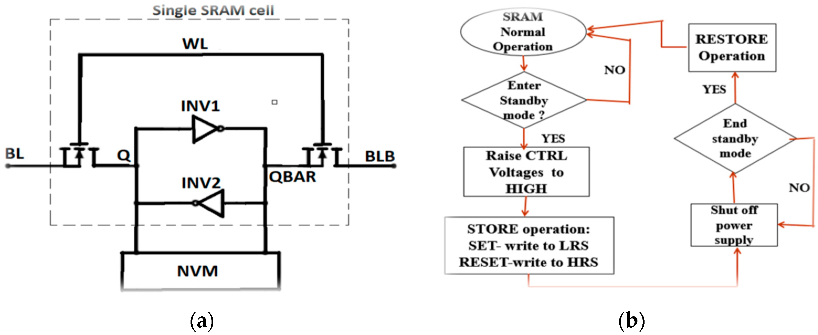
2. NVSRAM Cell Design
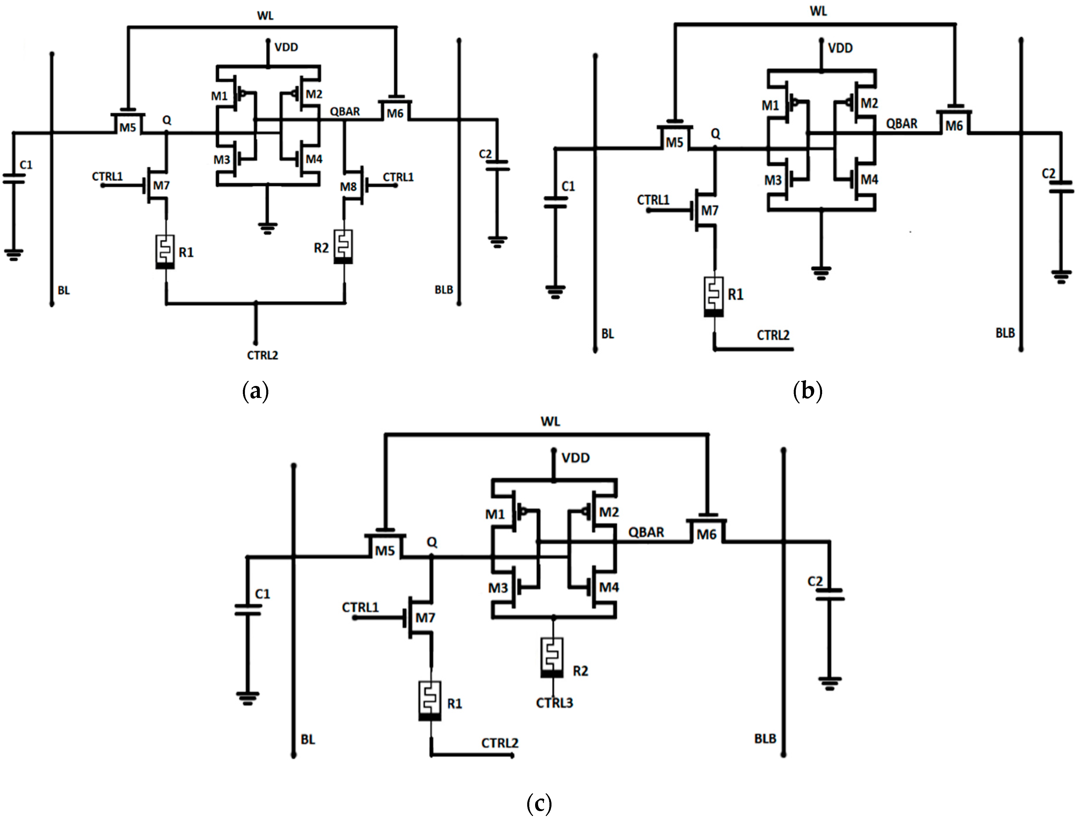
2.1. Existing NVSRAM Cells
2.1.1. 8T2R
2.1.2. 7T1R
2.1.3. 7T2R
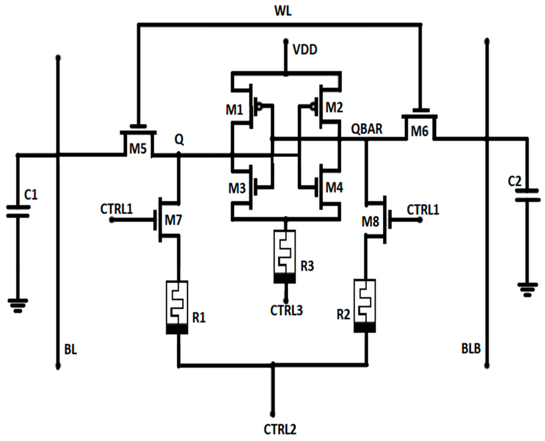
3. Proposed Symmetric 8T3R NVSRAM Cell
3.1. Structure
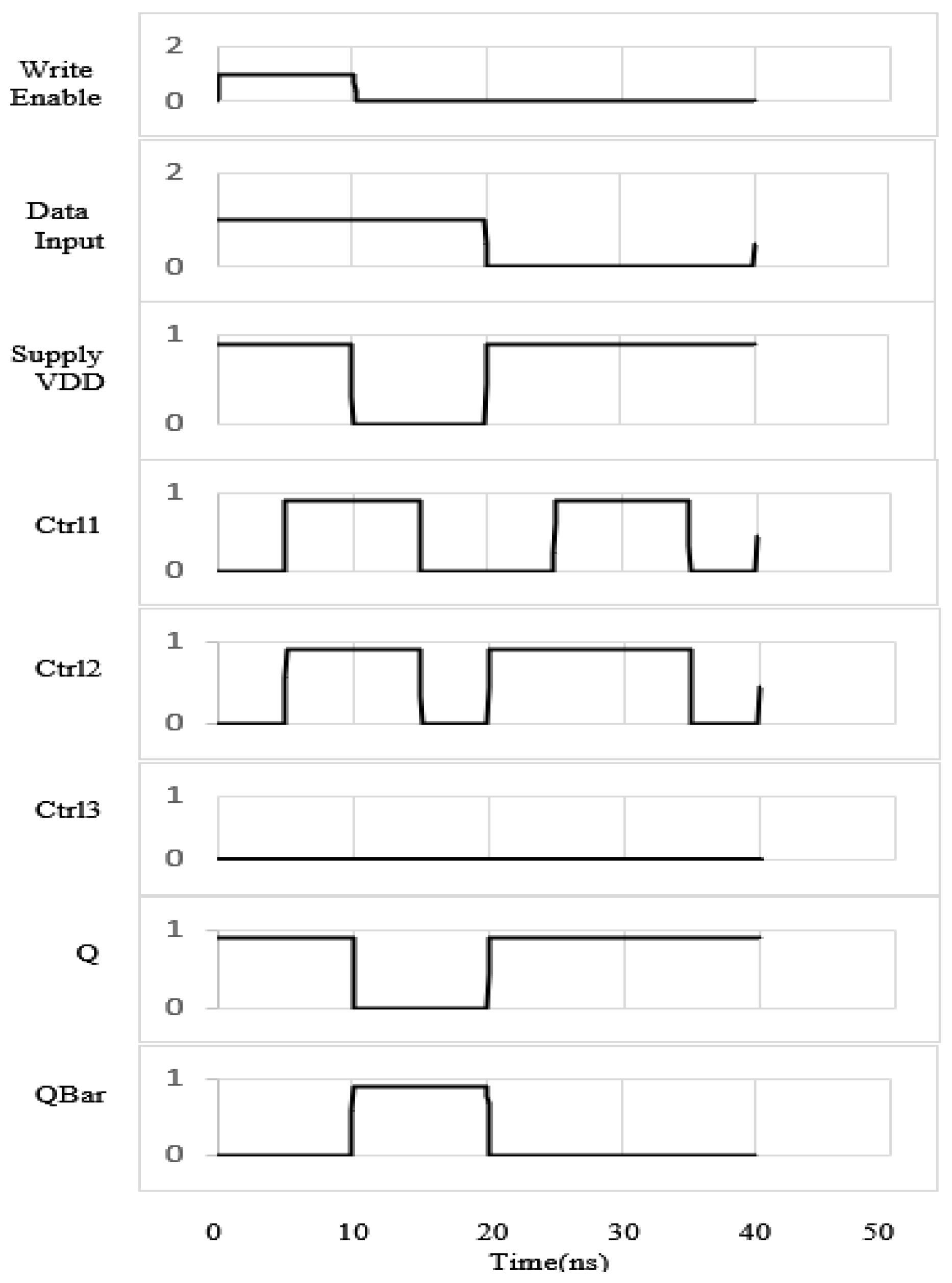
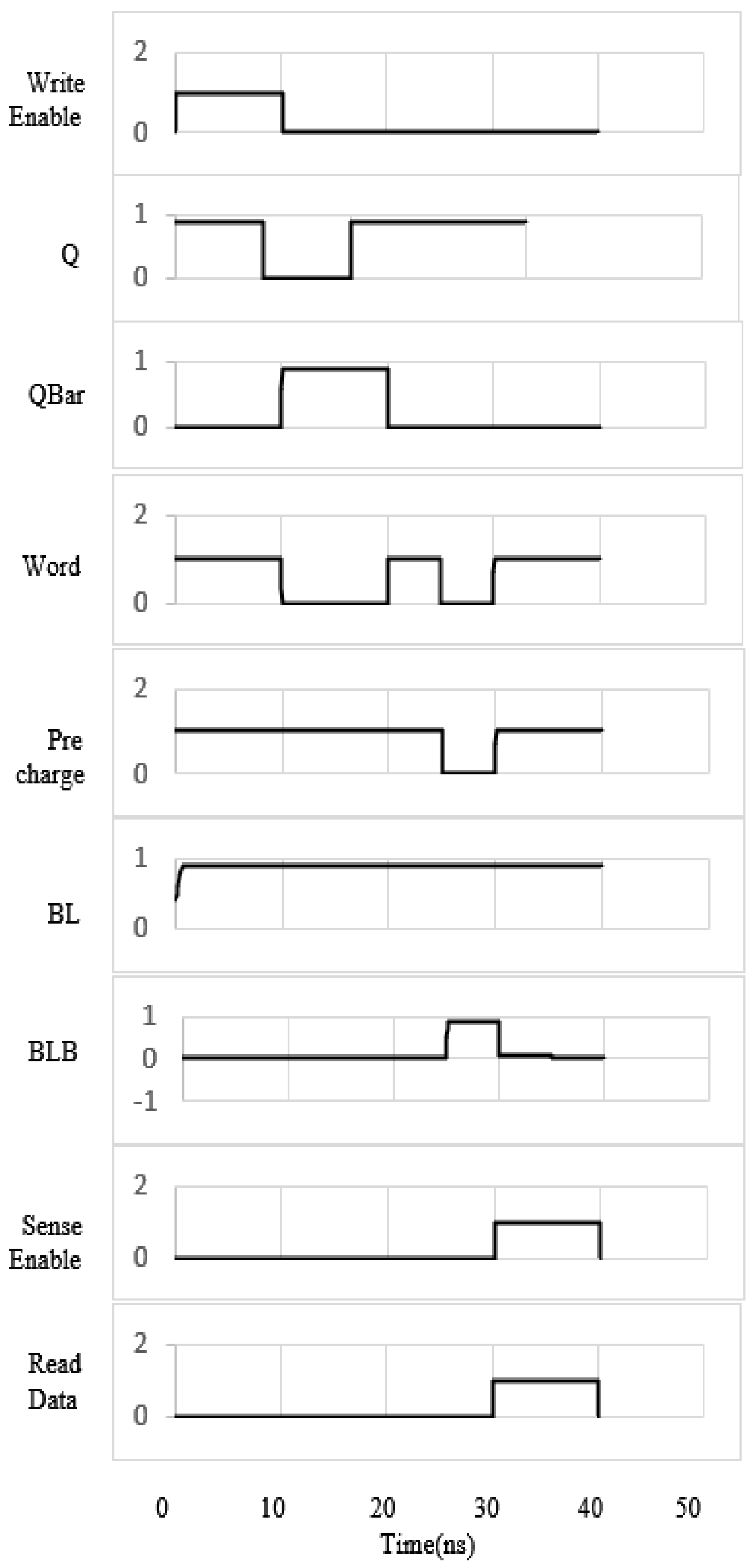
3.2. Normal SRAM Operation
3.3. RESET Operation
3.4. STORE Operation
3.5. POWER DOWN Operation
3.6. RESTORE Operation
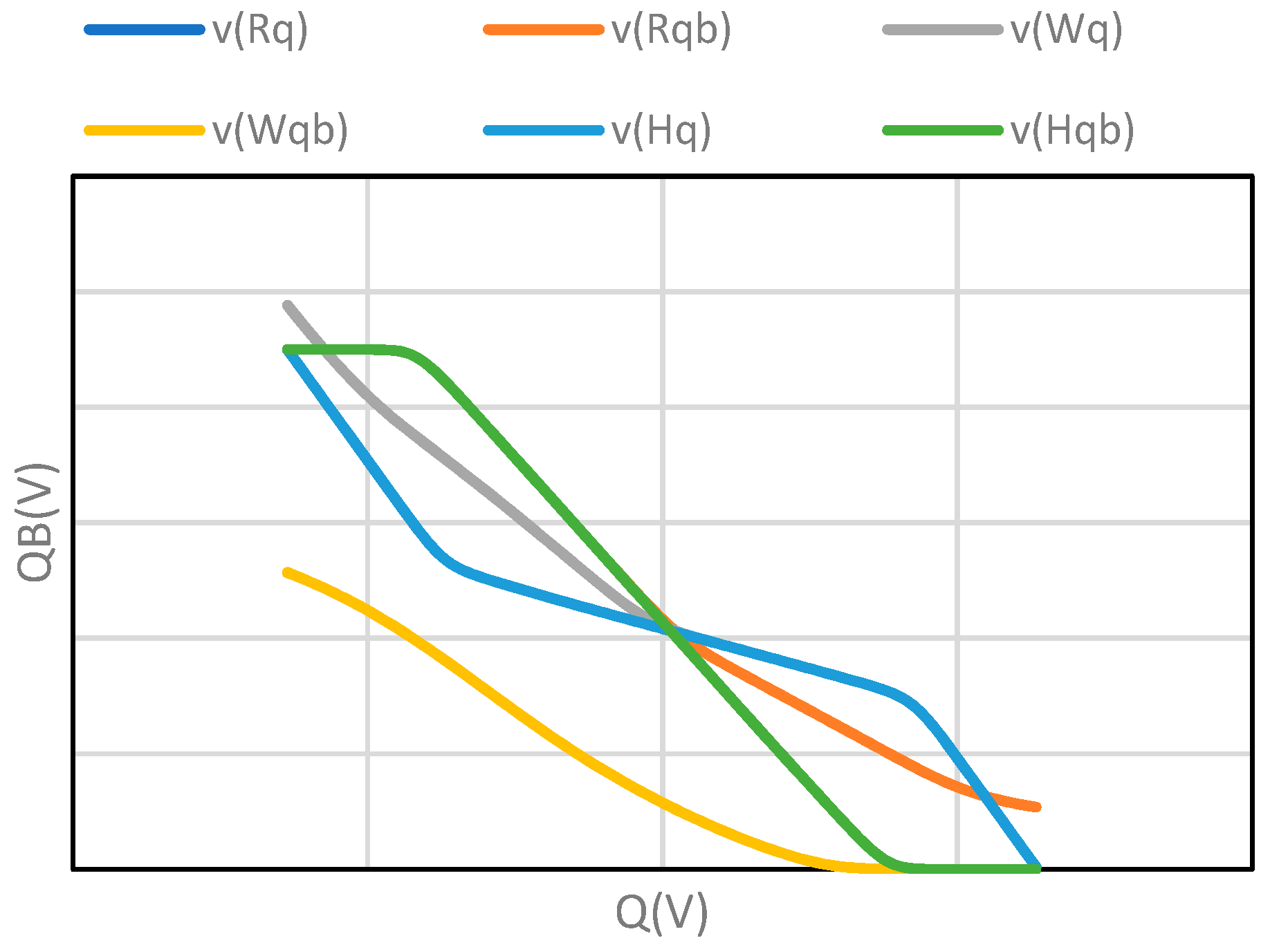
3.7. Evaluation of Non-Volatility
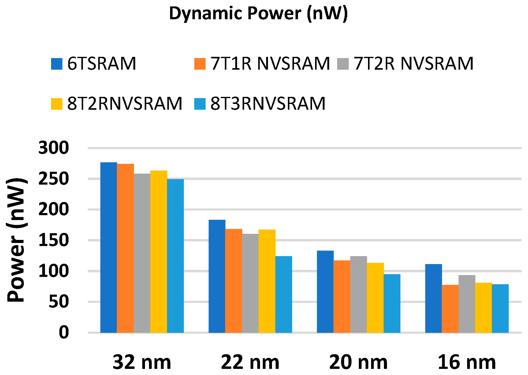
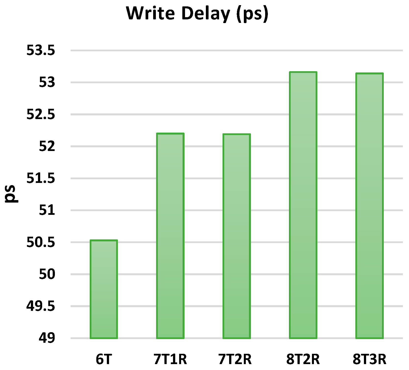
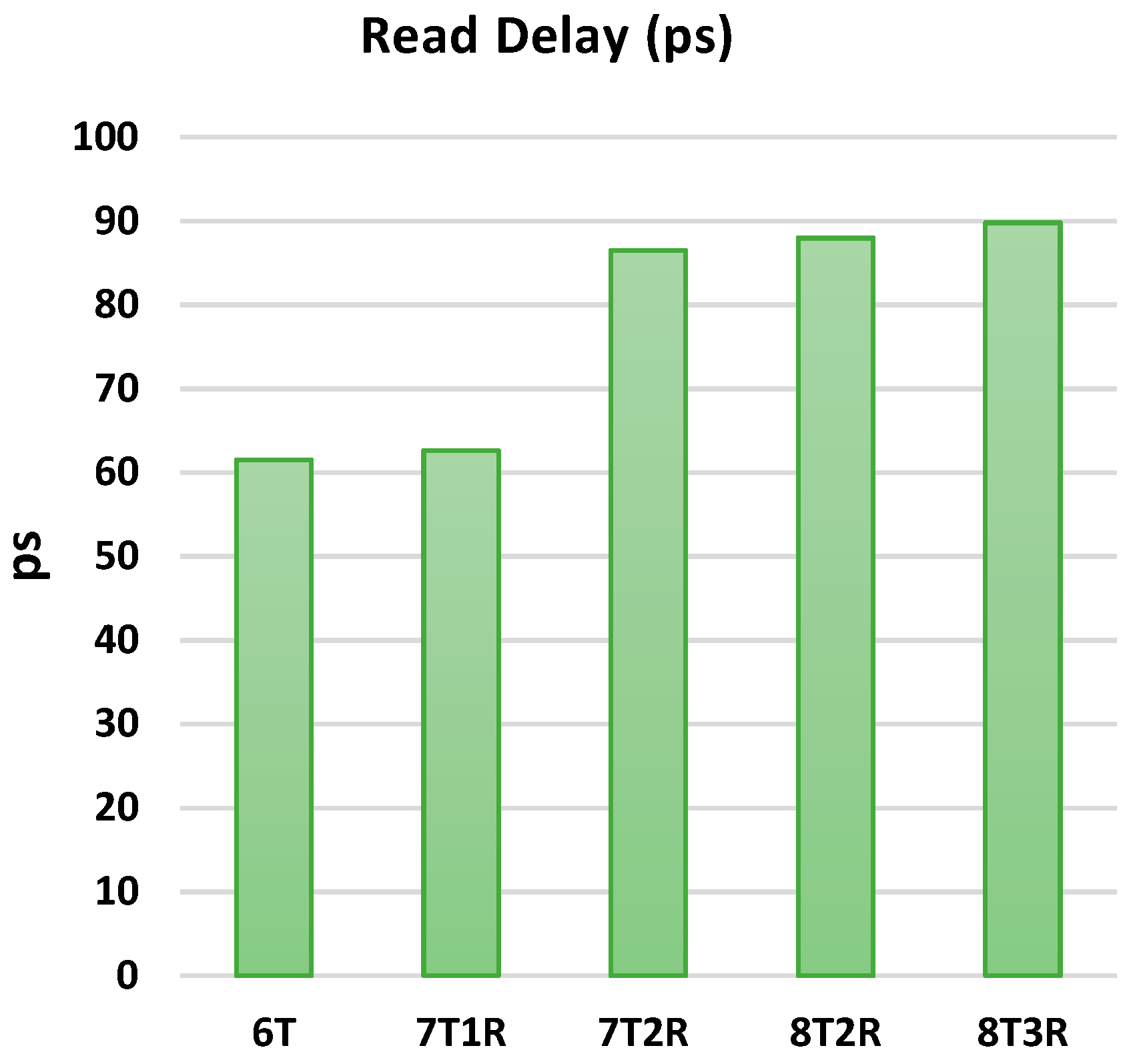
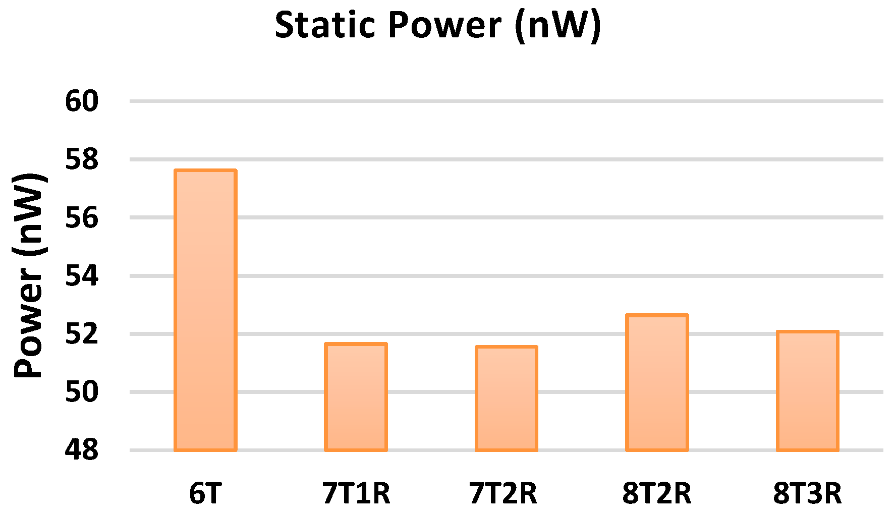
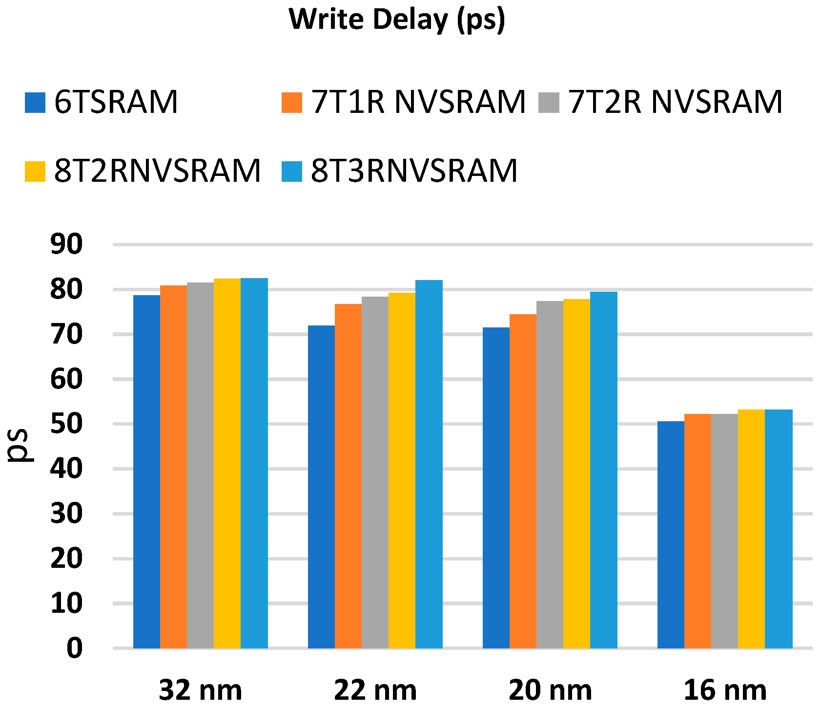
4. Simulation Results and Discussion
Performance Parameters of Proposed Symmetric 8T3R NVSRAM
5. Conclusions
Author Contributions
Funding
Institutional Review Board Statement
Informed Consent Statement
Data Availability Statement
Conflicts of Interest
References
- Meena, J.S.; Sze, S.M.; Chand, U.; Tseng, T.Y. Overview of emerging nonvolatile memory technologies. Nanoscale Res. Lett. 2014, 9, 526. [Google Scholar] [CrossRef] [PubMed] [Green Version]
- Zidan, M.A.; Fahmy, H.A.H.; Hussain, M.M.; Salama, K.N. Memristor-based memory: The sneak paths problem and solutions. Microelectron. J. 2013, 44, 176–183. [Google Scholar] [CrossRef] [Green Version]
- Biolek, D.; Ventra, M.D.I.; Pershin, Y.V. Reliable SPICE Simulations of Memristors, Memcapacitors and Meminductors Reliable Modeling of Memelements with SPICE. Radioengineering 2013, 22, 945. [Google Scholar]
- Buscarino, A.; Fortuna, L.; Frasca, M.; Gambuzza, V.L. A chaotic circuit based on Hewlett-Packard memristor A chaotic circuit based on Hewlett-Packard memristor. Chaos 2012, 22, 023136. [Google Scholar] [CrossRef] [PubMed]
- Cai, H.; Wang, Y.; Naviner, L.A.D.B.; Zhao, W. Robust Ultra-Low Power Non-Volatile Logic-in-Memory Circuits in FD-SOI Technology. IEEE Trans. Circuits Syst. I Regul. Pap. 2017, 64, 847–857. [Google Scholar] [CrossRef]
- Chen, P.; Member, S.; Yu, S. Compact Modeling of RRAM Devices and Its Applications in 1T1R and 1S1R Array Design. IEEE Trans. Electron Devices 2015, 62, 4022–4028. [Google Scholar] [CrossRef]
- Chiu, P.-F.; Chang, M.-F.; Wu, C.-W.; Chuang, C.-H.; Sheu, S.-S.; Chen, Y.-S.; Tsai, M.-J. Low store energy, low VDD min, 8T2R nonvolatile latch and SRAM with vertical-stacked resistive memory (memristor) devices for low power mobile applications. IEEE J. Solid-State Circuits 2012, 47, 1483–1496. [Google Scholar] [CrossRef]
- Chua, L.O. Memristor—The missing circuit element. EEE Trans. Circuit Theory 1971, 18, 507–519. [Google Scholar] [CrossRef]
- Garc, F.; Member, S.; Marisa, L. On the Design and Analysis of Reliable RRAM-CMOS Hybrid Circuits. IEEE Trans. Nanotechnol. 2017, 16, 514–522. [Google Scholar]
- Halawani, Y.; Mohammad, B.; Homouz, D.; Al-Qutayri, M.; Saleh, H. Modeling and Optimization of Memristor and STT-RAM-Based Memory for Low-Power Applications. IEEE Trans. Very Large Scale Integr. Syst. 2016, 24, 1003–1014. [Google Scholar] [CrossRef]
- Hu, J.; Stecklein, G.; Anugrah, Y.; Crowell, P.A.; Koester, S.J. Using Programmable Graphene Channels as Weights in Spin-Diffusive Neuromorphic Computing. IEEE J. Explor. Solid-State Comput. Devices Circuits 2018, 9231, 26–34. [Google Scholar] [CrossRef]
- Jiang, Z.; Yu, S.; Wu, Y.; Engel, J.H.; Guan, X.; Wong, H.-S.P. Verilog-A Compact Model for Oxide-based Resistive Random Access Memory (RRAM). In Proceedings of the 2014 International Conference on Simulation of Semiconductor Processes and Devices (SISPAD), Yokohama, Japan, 9–11 September 2014; pp. 41–44. [Google Scholar]
- Pal, S.; Bose, S.; Islam, A. Design of memristor based low power and highly reliable ReRAM cell. Microsyst. Technol. 2019. [Google Scholar] [CrossRef]
- Lehtonen, E.; Poikonen, J.H.; Laiho, M. Applications and limitations of memristive implication logic. In Proceedings of the 2012 IEEE International Symposium on Circuits and Systems (ISCAS), Seoul, Korea, 20–23 May 2012. [Google Scholar]
- Lu, W.; Lieber, C.M. Nanoelectronics from the bottom up. Nat. Mater. 2007, 6, 841–850. [Google Scholar] [CrossRef] [PubMed]
- Mountain, D.J.; Member, S.; Mclean, M.M. Memristor Crossbar Tiles in a Flexible, General Purpose Neural Processor. IEEE J. Emerg. Sel. Top. Circuits Syst. 2017, 8, 137–145. [Google Scholar] [CrossRef]
- Ni, L.; Liu, Z.; Yu, H.A.O.; Joshi, R.V. An Energy-Efficient Digital ReRAM-Crossbar-Based CNN with Bitwise Parallelism. IEEE J. Explor. Solid-State Comput. Devices Circuits 2017, 3, 37–46. [Google Scholar] [CrossRef]
- Pal, S.; Gupta, V.; Islam, A. Variation resilient low-power memristor-based synchronous flip-flops: Design and analysis. Microsyst. Technol. 2021, 27, 525–538. [Google Scholar] [CrossRef]
- Predictive Technology Model (PTM). 2012. Available online: https://ptm.asu.edu/ (accessed on 10 August 2019).
- Prasad, S.R.; Madhavi, B.K.; Kishore, K.L. Data-Retention Sleep Transistor CNTFET SRAM Cell Design at 32 nm Technology for Low-Leakage. In Proceedings of the 2nd International Conference on Advances in Information Technology and Mobile Communication—AIM 2012, Bangalore, India, 27–28 April 2012; pp. 362–368. [Google Scholar]
- Sakib, M.N.; Hassan, R.; Biswas, S.N.; Das, S.R. Memristor-Based High-Speed Memory Cell with Stable Successive Read Operation. IEEE Trans. Comput. Des. Integr. Circuits Syst. 2018, 37, 1037–1049. [Google Scholar] [CrossRef]
- Shin, S.; Kim, K.; Member, A.; Kang, S.-M. Memristor Applications for Programmable Analog ICs. IEEE Trans. Comput.-Aided Des. Integr. Circuits Syst. 2011, 10, 266–274. [Google Scholar]
- Singh, J.; Raj, B. Design and Investigation of 7T2M-NVSRAM With Enhanced Stability and Temperature Impact on Store/Restore Energy. IEEE Trans. Very Large Scale Integr. Syst. 2009, 27, 1322–1328. [Google Scholar] [CrossRef]
- Kanno, Y.; Mizuno, H.; Yasu, Y.; Hirose, K.; Shimazaki, Y.; Hoshi, T.; Miyairi, Y.; Ishii, T.; Yamada, T.; Irita, T.; et al. Hierarchical Power Distribution with Power Tree in Dozens of Power Domains for 90-nm Low-Power. IEEE J. Solid-State Circuits 2007, 42, 74–83. [Google Scholar] [CrossRef]
- Strachan, J.P.; Torrezan, A.C.; Miao, F.; Pickett, M.D.; Yang, J.J.; Yi, W.; Medeiros-Ribeiro, G.; Williams, S. State Dynamics and Modeling of Tantalum Oxide Memristors. IEEE Trans. Electron Devices 2013, 60, 2194–2202. [Google Scholar] [CrossRef]
- Strukov, D.B.; Snider, G.S.; Stewart, D.R.; Williams, R.S. The missing memristor found. Nature 2008, 453, 80–84. [Google Scholar] [CrossRef] [PubMed]
- Sun, J.; Shen, Y.; Yin, Q.; Xu, C. Compound synchronization of four memristor chaotic oscillator systems and secure communication Compound synchronization of four memristor chaotic oscillator systems and secure communication. Chaos Interdiscip. J. Nonlinear Sci. 2013, 23, 013140. [Google Scholar] [CrossRef] [PubMed]
- Swami, S.; Mohanram, K. Reliable Nonvolatile Memories: Techniques and Measures. IEEE Des. Test 2017, 34, 31–41. [Google Scholar] [CrossRef]
- Janniekode, U.M.; Somineni, R.P.; Naidu, C.D. Design and Performance Analysis of 6T SRAM Cell in Different Technologies and Nodes. Int. J. Perform. Eng. 2021, 17, 167–177. [Google Scholar]
- Yamamoto, S.; Shuto, Y.; Sugahara, S. Nonvolatile SRAM (NV-SRAM) using functional MOSFET merged with resistive switching devices. In Proceedings of the 2009IEEE Custom Integrated Circuits Conference, San Jose, CA, USA, 13–16 September 2009; pp. 531–534. [Google Scholar]
- Yang, J.J.; Strukov, D.B.; Stewart, D.R. Memristive devices for computing. Nat. Nanotechnol. 2013, 8, 13–24. [Google Scholar] [CrossRef] [PubMed]
- Wei, W.; Namba, K.; Han, J.; Lombardi, F. Design of a Nonvolatile 7T1R SRAM Cell for Instant-on Operation. IEEE Trans. Nanotechnol. 2014, 13, 905–916. [Google Scholar] [CrossRef]
- Palanisamy, S.; Thangaraju, B.; Khalaf, O.I.; Alotaibi, Y.; Alghamdi, S. Design and Synthesis of Multi-Mode Bandpass Filter for Wireless Applications. Electronics 2021, 10, 2853. [Google Scholar] [CrossRef]
- Rout, R.; Parida, P.; Alotaibi, Y.; Alghamdi, S.; Khalaf, O.I. Skin Lesion Extraction Using Multiscale Morphological Local Variance Reconstruction Based Watershed Transform and Fast Fuzzy C-Means Clustering. Symmetry 2021, 13, 2085. [Google Scholar] [CrossRef]
- García, N.O.; Velásquez, M.F.D.; Romero, C.A.T.; Monedero, J.H.O.; Khalaf, O.I. Remote Academic Platforms in Times of a Pandemic. Int. J. Emerg. Technol. Learn. 2021, 16, 121–131. [Google Scholar] [CrossRef]
- Khalaf, O.I.; Romero, C.A.T.; Pazhani, A.A.J.; Vinuja, G. VLSI Implementation of a High-Performance Nonlinear Image Scaling Algorithm. J. Healthc. Eng. 2021, 2021, 6297856. [Google Scholar] [CrossRef] [PubMed]
- Khalaf, O.I.; Abdulsahib, G.M. An Improved Efficient Bandwidth Allocation using TCP Connection for Switched Network. J. Appl. Sci. Eng. 2021, 24, 735–741. [Google Scholar] [CrossRef]
- Chen, Y.Y.; Govoreanu, B.; Goux, L.; Degraeve, R.; Fantini, A.; Kar, G.S.; Wouters, D.J.; Groeseneken, G.; Kittl, J.; Jurczak, M.; et al. Balancing SET/RESET Pulse for Endurance in 1T1R Bipolar RRAM. IEEE Trans. Electron Devices 2012, 59, 3243. [Google Scholar] [CrossRef]
- Grossi, A.; Vianello, E.; Sabry, M.M.; Barlas, M.; Grenouillet, L.; Coignus, J.; Beigne, E.; Wu, T.; Le, B.Q.; Wootters, M.K.; et al. Resistive RAM endurance: Array-level correction techniques targeting deep learning applications. IEEE Trans. Electron Devices 2019, 66, 1281–1288. [Google Scholar] [CrossRef]


| Parameter | WL (V) | VDD (V) | CTRL1 (V) | CTRL2 (V) |
|---|---|---|---|---|
| RESET | 0 | 1 | 0 | 1 |
| STORE | 1 | 1 | 1 | 1 |
| POWER DOWN | 0 | 0 | 0 | 0 |
| RESTORE | 1 | 1 | 1 | 1 |
| Parameter | 16 nm | 20 nm | 22 nm | 32 nm |
|---|---|---|---|---|
| VDD | 0.9 V | 0.9 V | 0.95 V | 1 V |
| CTRL1, CTRL2, CTRL3 | 0.9 V | 0.9 V | 0.95 V | 1 V |
| RSET (LRS) | 100 Ω | |||
| RRESET (HRS) | 16 KΩ | |||
| Temperature | 25 °C | |||
| Parameters | 16 nm | 20 nm | 22 nm | 32 nm |
|---|---|---|---|---|
| Write Delay (ps) | 33.87 | 53.89 | 57.81 | 66.84 |
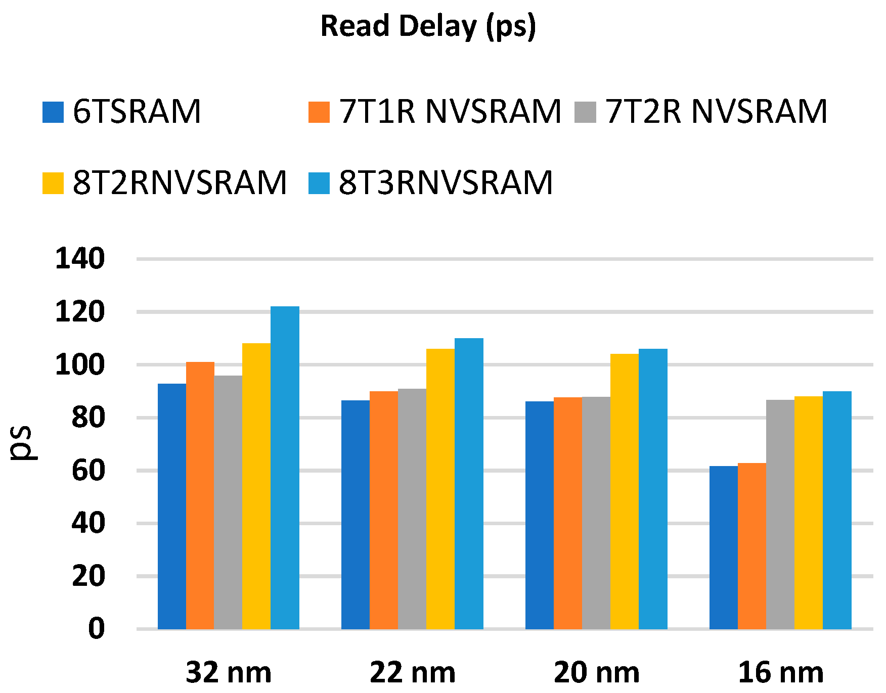
| Read Delay (ps) | 145.7 | 155.3 | 172 | 92.41 |
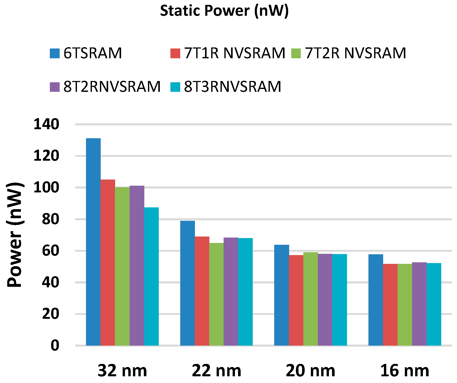
| Static Power (nW) | 2.78 | 2.78 | 0.34 | 5.17 |
| Dynamic Power | 14.16 | 17.52 | 9.54 | 18.06 |
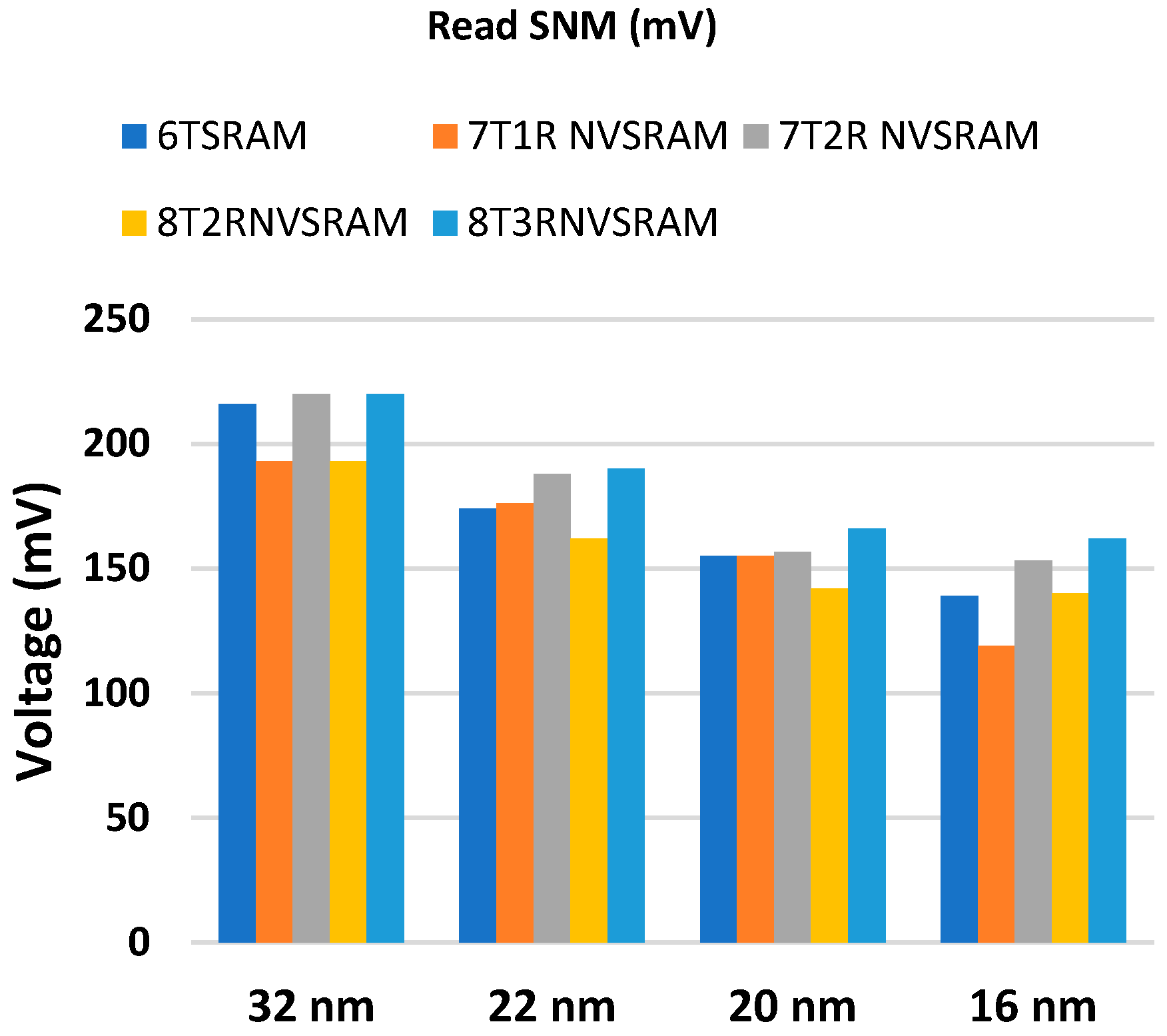
| RSNM (mv) | 170 | 148 | 166 | 220 |
| WSNM (mv) | 554 | 536 | 560 | 636 |
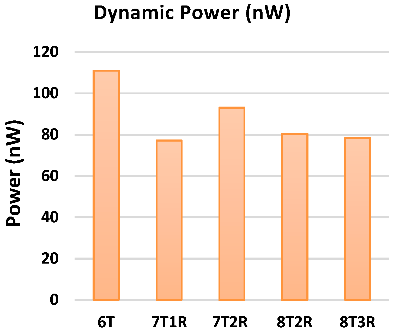
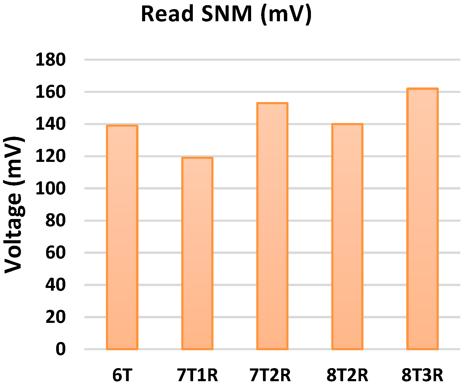
| Parameters | 6T | 7T1R | 7T2R | 8T2R | Proposed NVSRAM |
|---|---|---|---|---|---|
| Write Delay (ps) | 50.53 | 52.2 | 52.19 | 53.16 | 53.14 |
| Read Delay (ps) | 61.52 | 62.63 | 86.52 | 87.98 | 89.8 |
| Static Power (nW) | 57.62 | 51.65 | 51.55 | 52.64 | 52.08 |
| Dynamic Power (nW) | 111 | 77.18 | 93.08 | 80.48 | 78.34 |
| Total Power Dissipation (nW) | 168.62 | 128.83 | 144.63 | 133.12 | 130.42 |
| RSNM (mV) | 139 | 119 | 153 | 140 | 162 |
| WSNM (mV) | 462 | 491 | 539 | 501 | 539 |
Publisher’s Note: MDPI stays neutral with regard to jurisdictional claims in published maps and institutional affiliations. |
© 2022 by the authors. Licensee MDPI, Basel, Switzerland. This article is an open access article distributed under the terms and conditions of the Creative Commons Attribution (CC BY) license (https://creativecommons.org/licenses/by/4.0/).
Share and Cite
Janniekode, U.M.; Somineni, R.P.; Khalaf, O.I.; Itani, M.M.; Chinna Babu, J.; Abdulsahib, G.M. A Symmetric Novel 8T3R Non-Volatile SRAM Cell for Embedded Applications. Symmetry 2022, 14, 768. https://doi.org/10.3390/sym14040768
Janniekode UM, Somineni RP, Khalaf OI, Itani MM, Chinna Babu J, Abdulsahib GM. A Symmetric Novel 8T3R Non-Volatile SRAM Cell for Embedded Applications. Symmetry. 2022; 14(4):768. https://doi.org/10.3390/sym14040768
Chicago/Turabian StyleJanniekode, Uma Maheshwar, Rajendra Prasad Somineni, Osamah Ibrahim Khalaf, Malakeh Muhyiddeen Itani, J. Chinna Babu, and Ghaida Muttashar Abdulsahib. 2022. "A Symmetric Novel 8T3R Non-Volatile SRAM Cell for Embedded Applications" Symmetry 14, no. 4: 768. https://doi.org/10.3390/sym14040768
APA StyleJanniekode, U. M., Somineni, R. P., Khalaf, O. I., Itani, M. M., Chinna Babu, J., & Abdulsahib, G. M. (2022). A Symmetric Novel 8T3R Non-Volatile SRAM Cell for Embedded Applications. Symmetry, 14(4), 768. https://doi.org/10.3390/sym14040768