
Surface Characterization of New Azulene-Based CMEs for Sensing

 ,
,  ,
,
Abstract
:1. Introduction
2. Materials and Methods
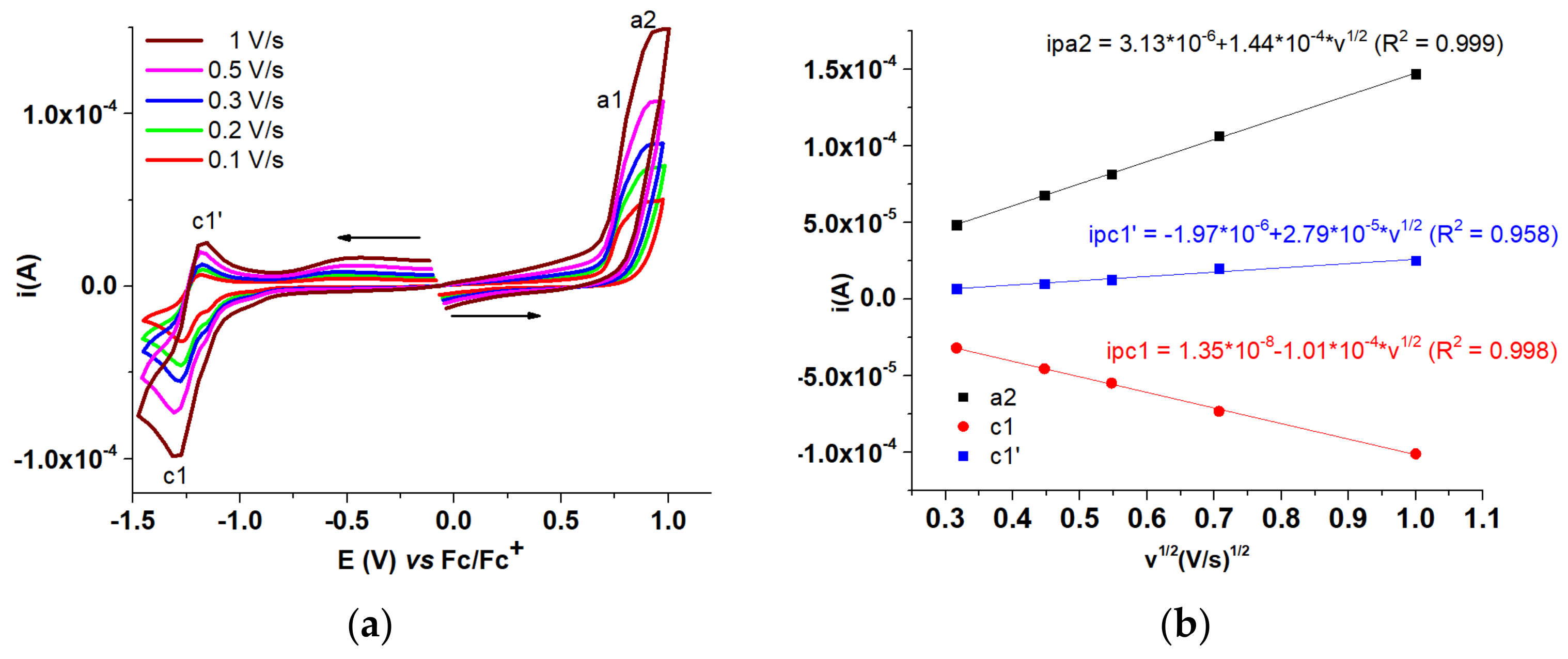
3. Results and Discussion
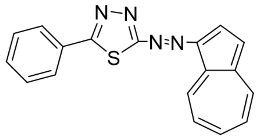
3.1. Immobilization of T Complexing Monomer on Electrode Surfaces
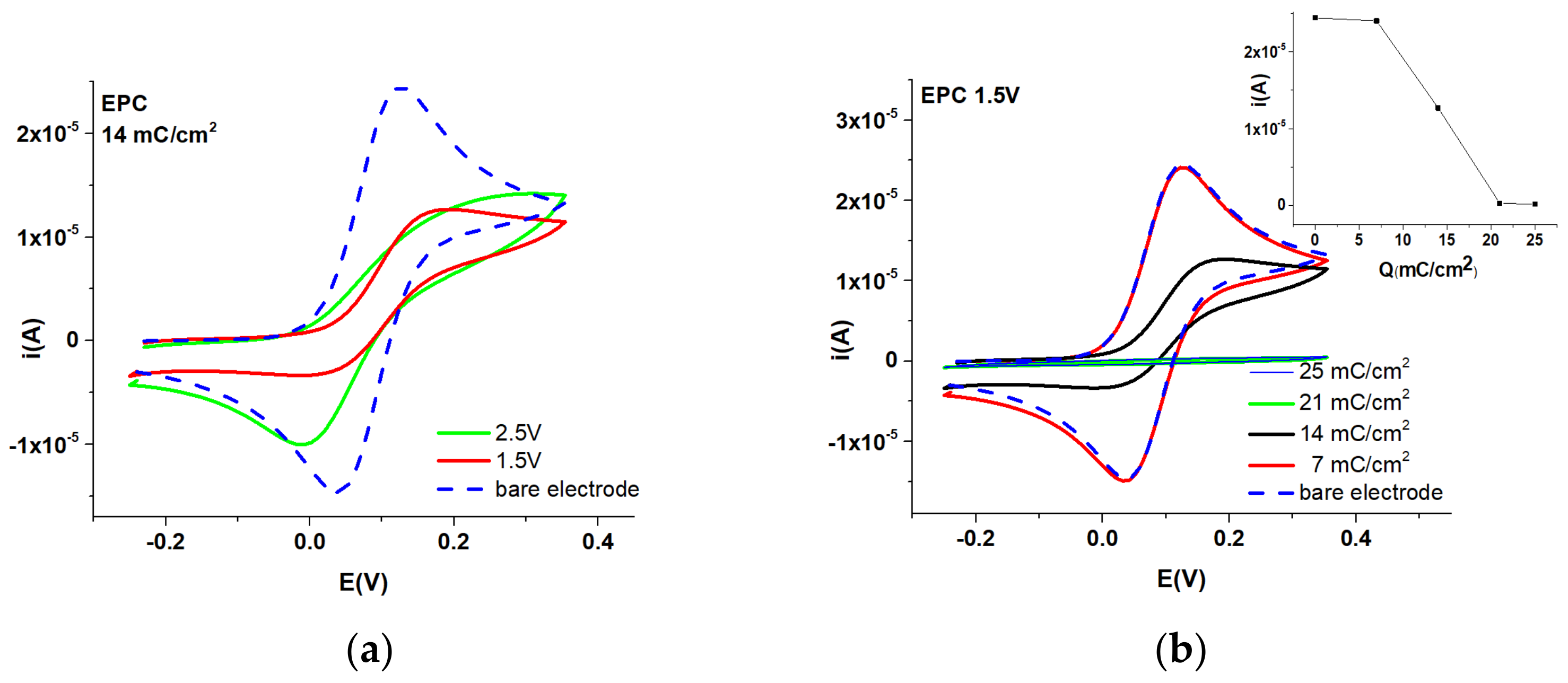
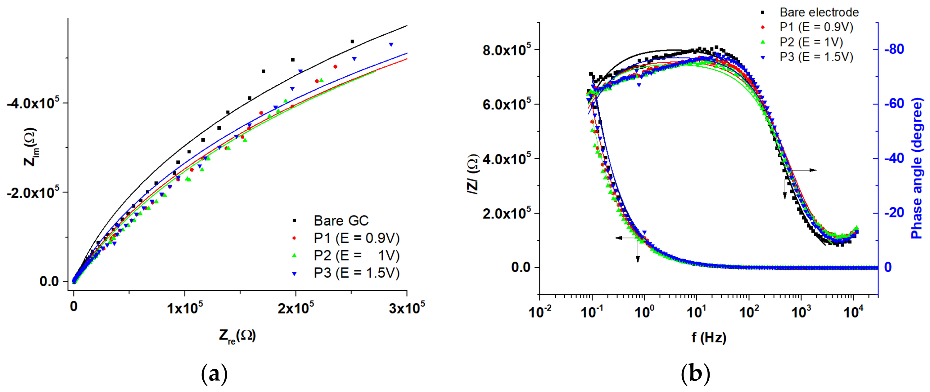
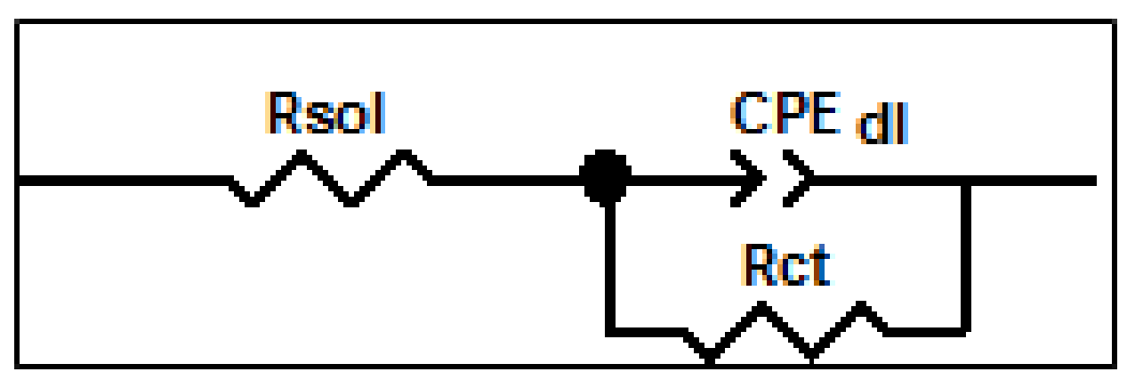
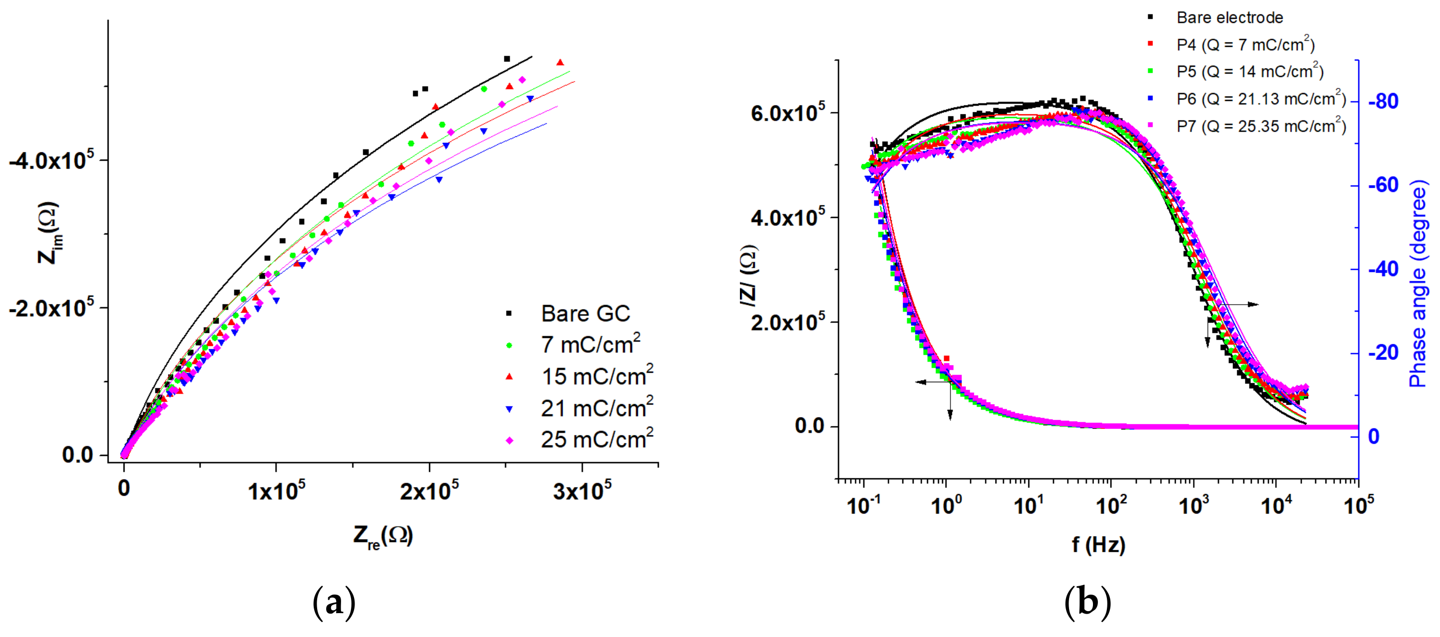
3.2. Studies by EIS
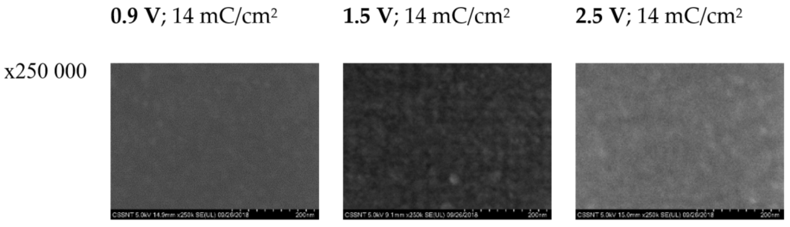
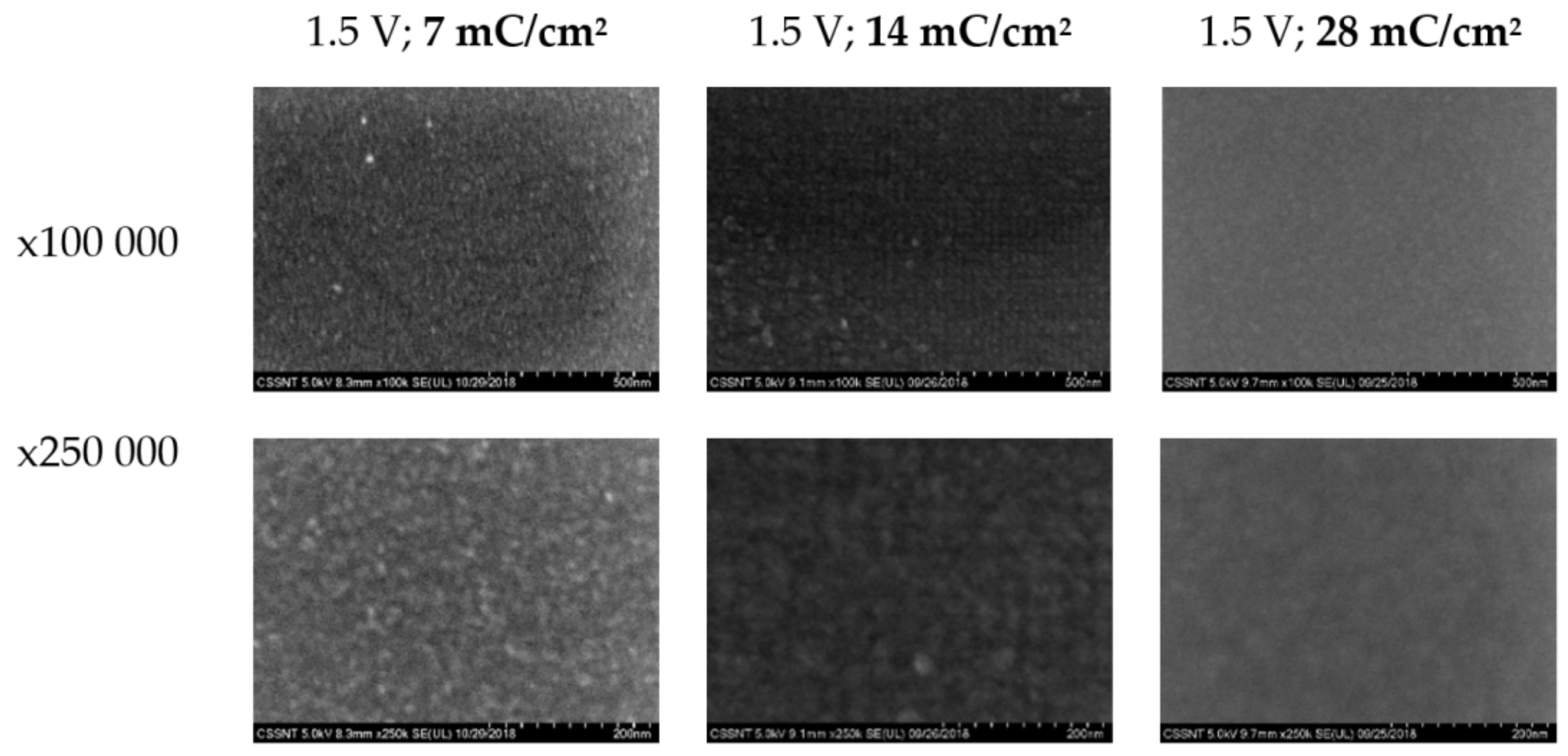
3.3. Studies by SEM
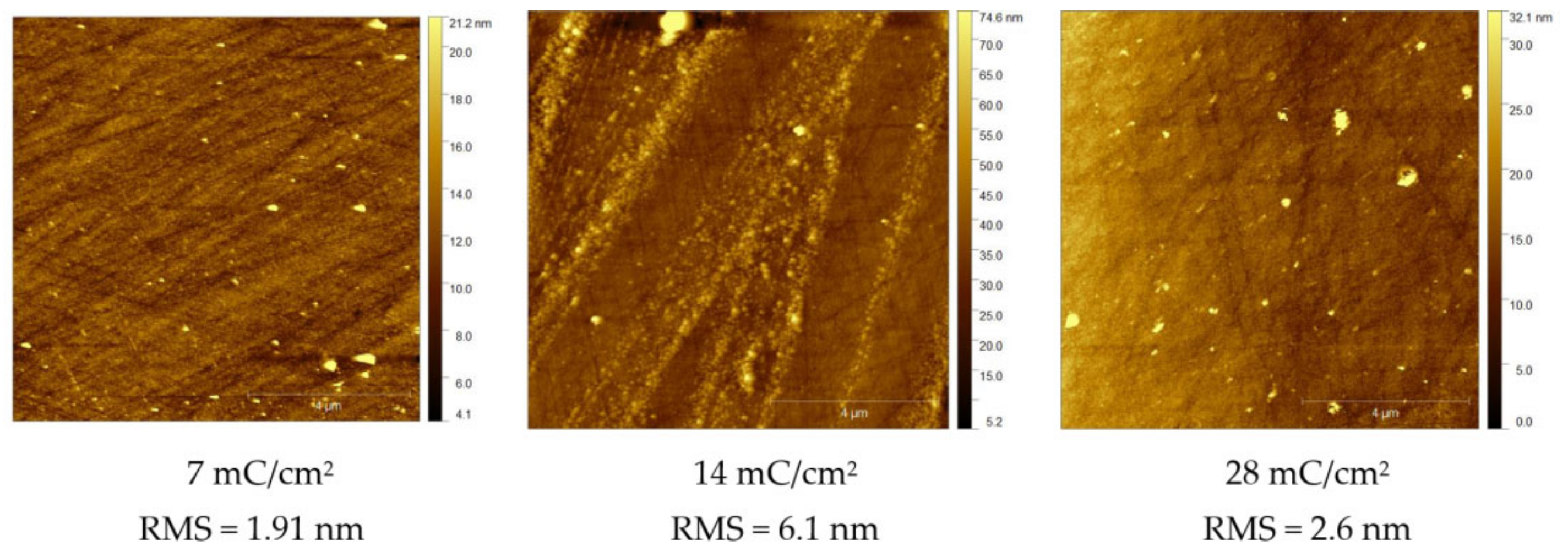
3.4. Studies by AFM
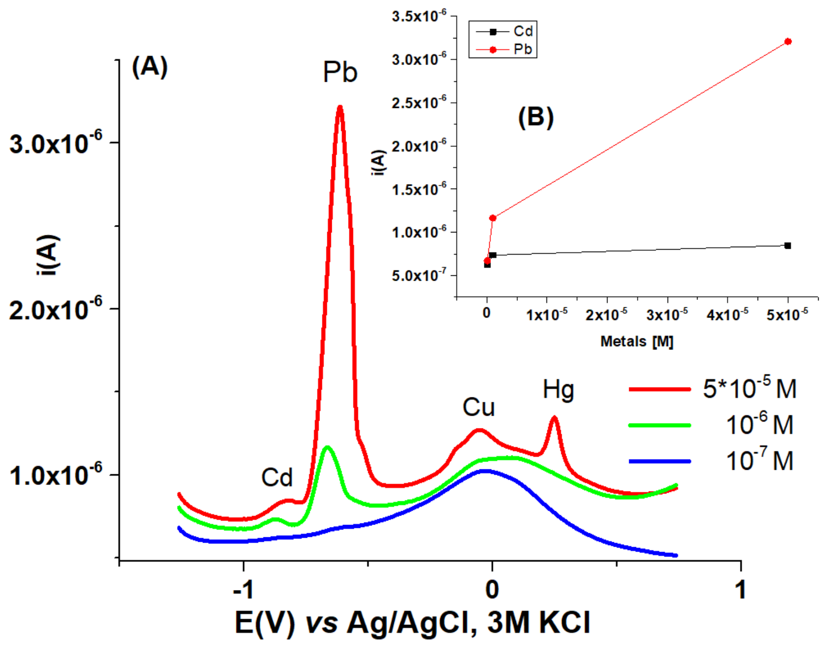
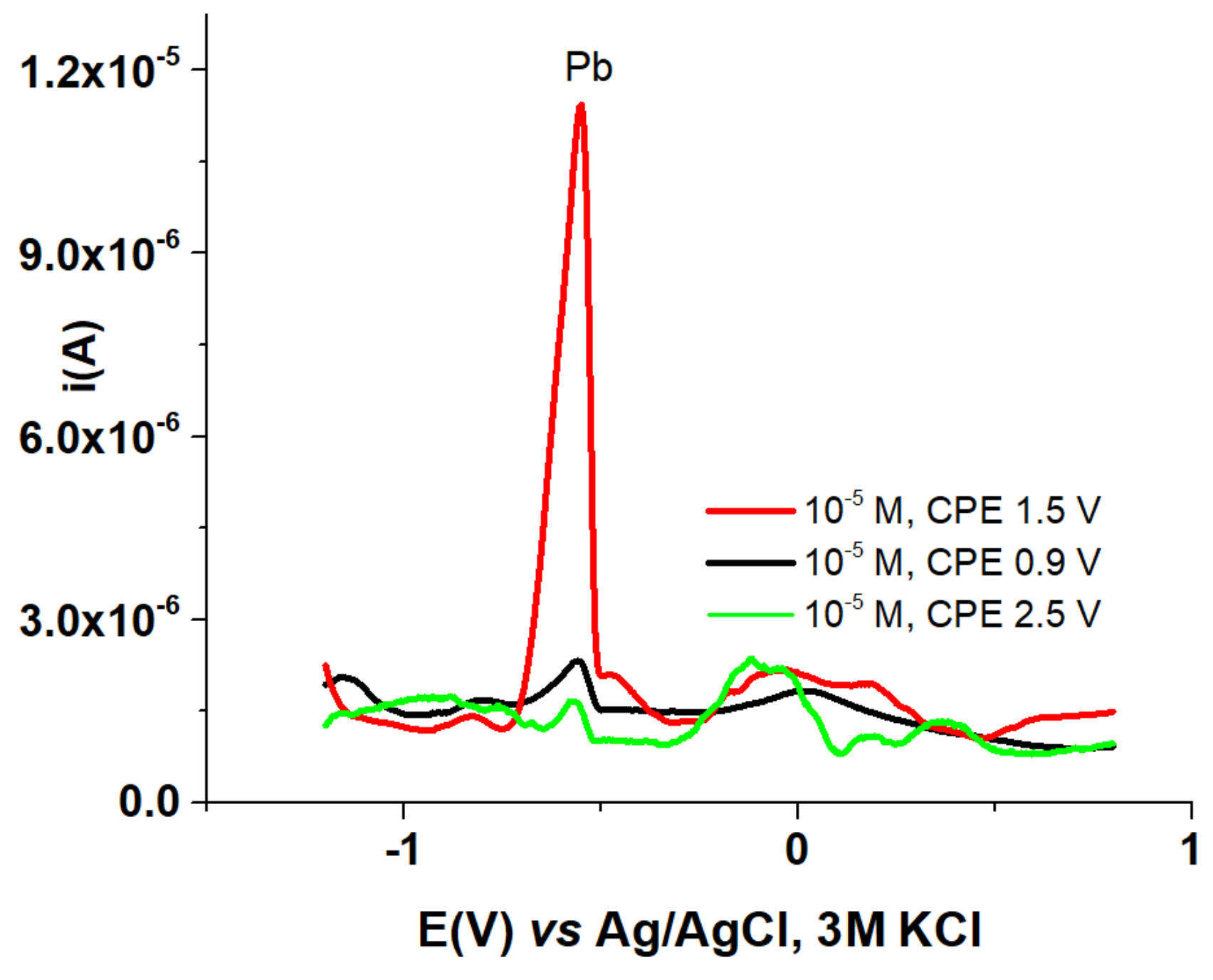
3.5. HMs Sensing
3.6. Electrochemical Characterization of T
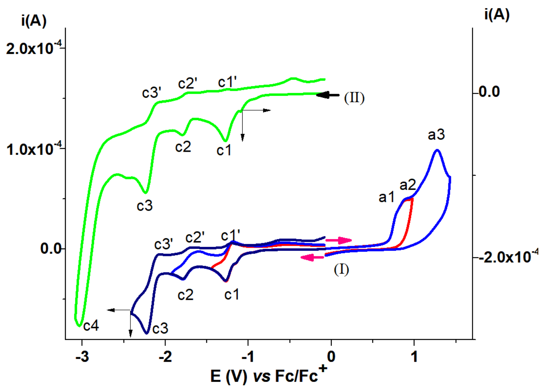
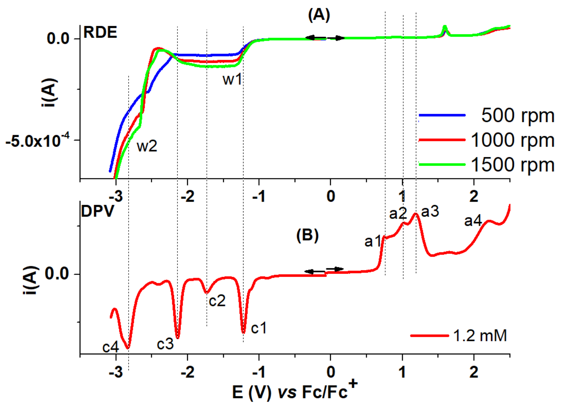
3.6.1. CV and DPV
3.6.2. RDE Studies
4. Global View of Results
5. Conclusions
Supplementary Materials
Author Contributions
Funding
Institutional Review Board Statement
Informed Consent Statement
Data Availability Statement
Acknowledgments
Conflicts of Interest
References
- Rydz, J.; Šišková, A.; Eckstein, A.A. Scanning Electron Microscopy and Atomic Force Microscopy: Topographic and Dynamical Surface Studies of Blends, Composites, and Hybrid Functional Materials for Sustainable Future. Adv. Mater. Sci. Eng. 2019, 2019, 6871785. [Google Scholar] [CrossRef] [Green Version]
- Maver, U.; Velnar, T.; Gaberšček, M.; Planinšek, O.; Finšgar, M. Recent progressive use of atomic force microscopy in biomedical applications. Trends Analyt. Chem. 2016, 80, 96–111. [Google Scholar] [CrossRef] [Green Version]
- Nguyen-Tri, P.; Ghassemi, P.; Carriere, P.; Nanda, S.; Assadi, A.A.; Nguyen, D.D. Recent Applications of Advanced Atomic Force Microscopy in Polymer Science: A Review. Polymers 2020, 12, 1142. [Google Scholar] [CrossRef] [PubMed]
- Jurczyk, S.; Musioł, M.; Sobota, M.; Klim, M.; Hercog, A.; Kurcok, P.; Janeczek, H.; Rydz, J. (Bio)Degradable Polymeric Materials for Sustainable Future—Part 2: Degradation Studies Of P(3hb-Co-4hb)/Cork Composites in Different Environments. Polymers 2019, 11, 547. [Google Scholar] [CrossRef] [Green Version]
- Shao, G.; Wang, J.; Zhang, S.; Wang, Y.; Wang, W.; Wang, H.-X. Surface Morphology and Microstructure Evolution of Single Crystal Diamond during Different Homoepitaxial Growth Stages. Materials 2021, 14, 5964. [Google Scholar] [CrossRef]
- Shinmura, K.; Kawasaki, H.; Baba, S.; Ohta, I.; Kato, H.; Yasuda, H.; Yamada, S.; Misawa, K.; Sugimoto, K.; Osawa, S.; et al. Utility of Scanning Electron Microscopy Elemental Analysis Using the ‘NanoSuit’ Correlative Light and Electron Microscopy Method in the Diagnosis of Lanthanum Phosphate Deposition in the Esophagogastroduodenal Mucosa. Diagnostics 2020, 10, 1. [Google Scholar] [CrossRef] [Green Version]
- Razus, A.C.; Birzan, L.; Cristea, M.; Tecuceanu, V.; Draghici, C.; Hanganu, A.; Maganu, M.; Pintilie, L.; Ungureanu, E.M. New (Azulen-1-Yldiazenyl)-Heteroaromatic Compounds Containing 1,2,5-Thiadiazol-3-Yl Moieties. Rev. Chim. 2019, 70, 1518–1529. [Google Scholar] [CrossRef]
- Garcia-Amorós, J.; Reig, M.; Cidália, M.; Castro, R.; Cuadrado, A.; Manuela, M.; Raposo, M.; Velasco, D. Molecular photo-oscillators based on highly accelerated heterocyclic azo dyes in nematic liquid crystals. Chem. Commun. 2014, 50, 6704–6706. [Google Scholar] [CrossRef] [Green Version]
- Yan, Z.; Guang, S.; Xu, H.; Liu, X.-Y. Quinoline-based azo derivative assembly: Optical limiting property and enhancement mechanism. Dyes Pigm. 2013, 99, 720–726. [Google Scholar] [CrossRef]
- Zhang, Y.; Pei, S.; Wang, Y.; Cui, Z.; Li, N.; Zhu, Y.; Zhang, H.; Jiang, Z. Synthesis, characterization, and photoresponsive behavior of a series of azobenzene-containing side-chain poly(ether sulfone)s with various lengths of flexible spacers. Dyes Pigm. 2013, 99, 1117–1123. [Google Scholar] [CrossRef]
- Zhu, Y.; Zhou, Y.; Wang, X. Photoresponsive behavior of two well-defined azo polymers with different electron-withdrawing groups on push–pull azo chromophores. Dyes Pigm. 2013, 99, 209–219. [Google Scholar] [CrossRef]
- Solomon, R.V.; Jagadeesan, R.; Vedha, S.A.; Venuvanalingam, P. A DFT/TDDFT modelling of bithiophene azo chromophores for optoelectronic applications. Dyes Pigm. 2014, 100, 261–268. [Google Scholar] [CrossRef]
- Arrigan, D.W.M. Voltammetric Determination of Trace Metals and Organics after Accumulation at Modified Electrodes. Analyst 1994, 119, 1953–1966. [Google Scholar] [CrossRef]
- Cristea, M.; Bîrzan, L.; Dumitrascu, F.; Enache, C.; Tecuceanu, V.; Hanganu, A.; Drăghici, C.; Deleanu, C.; Nicolescu, A.; Maganu, M.; et al. 1-Vinylazulenes with Oxazolonic Ring-Potential Ligands for Metal Ion Detectors; Synthesis and Products Properties. Symmetry 2021, 13, 1209. [Google Scholar] [CrossRef]
- Wang, F.; Lai, Y.H.; Han, M.Y. Stimuli-Responsive Conjugated Copolymers Having Electro-Active Azulene and Bithiophene Units in the Polymer Skeleton: Effect of Protonation and p-Doping on Conducting Properties. Macromolecules 2004, 37, 3222–3230. [Google Scholar] [CrossRef]
- Razus, A.C. Azulene Moiety as Electron Reservoir in Positively Charged Systems; A Short Survey. Symmetry 2021, 13, 526. [Google Scholar] [CrossRef]
- Stefaniu, A.; Pintilie, L.; Anastasoaie, V.; Ungureanu, E.-M. In silico Evaluation of Antimicrobial Activity of Some Thiadiazoles Using Molecular Docking Approach. Chem. Proc. 2021, 3, 116. [Google Scholar] [CrossRef]
- Tzvetkova, P.; Vassileva, P.; Nickolov, R. Modified Silica Gel With 5-Amino-1,3,4-Thiadiazole-2-Thiol for Heavy Metal Ions Removal. J. Porous Mater. 2010, 17, 459–463. [Google Scholar] [CrossRef]
- Li, C.; Huang, S.; Min, C.; Du, P.; Xia, Y.; Yang, C.; Huang, Q. Highly Productive Synthesis, Characterization, And Fluorescence and Heavy Metal Ion Adsorption Properties of Poly(2,5-Dimercapto-1,3,4-Thiadiazole) Nanosheets. Polymers 2018, 10, 24. [Google Scholar] [CrossRef] [Green Version]
- Skrzypek, S.; Kasprzak, M.; Ciesielski, W. Cathodic Stripping Voltammetry Of 2-Mercapto-5-Methyl-1,3,4-Thiadiazol And 2,5-Dimercapto-1,3,4-Thiadiazol At A Controlled-Growth Mercury Drop Electrode. J. Anal. Chem. 2005, 60, 978–981. [Google Scholar] [CrossRef]
- Ungureanu, E.M.; Buica, G.O.; Razus, A.C.; Birzan, L.; Weisz, R.; Bujduveanu, M.-R. Electrochemical Study on 4-(Azulen-1-Yl)-2,6-Bis(2-Furyl)- And 4-(Azulen-1-Yl)-2,6-Bis(2-Thienyl)-Pyridines. Rev. Chim. 2012, 63, 27–33. [Google Scholar] [CrossRef]
- Ungureanu, E.-M.; Razus, A.C.; Birzan, L.; Cretu, M.S.; Buica, G.-O. Electrochemical study of azo–azulene compounds. Electrochim. Acta 2008, 53, 7089–7099. [Google Scholar] [CrossRef]
- Pop, M.D.; Brincoveanu, O.A.; Cristea, M.; Buica, G.-O.; Enachescu, M.; Ungureanu, E.-M. AFM and SEM Characterization of Chemically Modified Electrodes Based On 5-[(Azulen-1-Yl) Methylene]-2-Thioxothiazolidin-4-one. Rev. Chim. 2017, 68, 2799–2803. [Google Scholar] [CrossRef]
- Suominen, M.; Lehtimäki, S.; Yewale, R.; Damlin, P.; Tuukkanen, S.; Kvarnström, C. Electropolymerized polyazulene as active material in flexible supercapacitors. J. Power Sources 2017, 356, 181–190. [Google Scholar] [CrossRef]
- Hea, N.; Höflerb, L.; Latonena, R.-M.; Lindforsa, T. Influence of hydrophobization of the polyazulene ion-to-electron transducer on the potential stability of calcium-selective solid-contact electrodes. Sens. Actuators B Chem. 2015, 207, 918–925. [Google Scholar] [CrossRef]
- Lete, C.; Gadgil, B.; Kvarnström, C. The electrochemistry of copolymer films based on azulene and 3 thiophene acetic acid. J. Electroanal. Chem. 2017, 742, 30–36. [Google Scholar] [CrossRef]
- Buica, G.-O.; Ungureanu, E.-M.; Birzan, L.; Razus, A.C.; Mandoc (Popescu), L.-R. Voltammetric sensing of lead and cadmium using poly(4-azulen-1-yl-2,6-bis(2-thienyl)pyridine) complexing films. J. Electroanal. Chem. 2013, 693, 67–72. [Google Scholar] [CrossRef]
- Enache, L.-B.; Anastasoaie, V.; Birzan, L.; Ungureanu, E.-M.; Diao, P.; Enachescu, M. Polyazulene-Based Materials for Heavy Metal Ion Detection. 2. (E)-5-(Azulen-1-Yldiazenyl)-1htetrazole- Modified Electrodes for Heavy Metal Sensing. Coatings 2020, 10, 869. [Google Scholar] [CrossRef]
- Numan, A.; Gill, A.A.S.; Rafique, S.; Guduri, M.; Zhan, Y.; Maddiboyina, B.; Li, L.; Singh, S.; Dang, N.N. Rationally engineered nanosensors: A novel strategy for the detection of heavy metal ions in the environment. J. Hazard. Mater. 2021, 409, 124493. [Google Scholar] [CrossRef]


| T-CMEs | Potential (V) | Charge Density (mC/cm2) |
|---|---|---|
| P1 | +0.9 | 14 |
| P2 | +1.0 | 14 |
| P3 | +1.5 | 14 |
| P4 | +1.5 | 7 |
| P5 | +1.5 | 14 |
| P6 | +1.5 | 21 |
| P7 | +1.5 | 25 |
| T-CME Films Characteristics | Rsol(Ω) | 106·Rct (Ω) | CPEdl | χ2 | |
|---|---|---|---|---|---|
| C (µF) | n | ||||
| P1 (0.9 V; 14 mC/cm2) | 196 | 1.87 | 2.19 | 0.85 | 9.082·10−3 |
| P2 (1 V; 14 mC/cm2) | 208 | 1.95 | 2.42 | 0.84 | 1.08·10−2 |
| P3 (1.5 V; 14 mC/cm2) | 213 | 1.81 | 1.84 | 0.87 | 1.13·10−2 |
| GC (0 V; 0 mC/cm2) | 210 | 2 | 1.86 | 0.9 | 1.081·10−2 |
| T-CME Films Characteristics | Rsol (Ω) | 106·Rct (Ω) | CPEdl | χ2 | |
|---|---|---|---|---|---|
| C (µF) | n | ||||
| P4 (1.5 V; 7 mC/cm2) | 204.5 | 2.034 | 2.23 | 0.86 | 8.003·10−3 |
| P5 (1.5 V; 14 mC/cm2) | 213 | 1.81 | 1.84 | 0.87 | 1.13·10−2 |
| P6 (1.5 V; 21 mC/cm2) | 187 | 1.65 | 2.02 | 0.85 | 1.45·10−2 |
| P7 (1.5 V; 28 mC/cm2) | 185 | 1.815 | 1.95 | 0.84 | 1.52·10−2 |
| GC (0 V; 0 mC/cm2) | 209.7 | 2 | 1.86 | 0.9 | 1.086·10−2 |
| Peak | Method | Peak Characterization | |
|---|---|---|---|
| CV | DPV | ||
| a1 | 0.88 | 0.74 | irreversible |
| a2 | - | 1.01 | irreversible |
| a3 | 1.27 | 1.18 | irreversible |
| a4 | 2.40 | 2.20 | irreversible |
| c1 c1′ | −1.27 −1.18 | −1.22 - | reversible |
| c2 c2′ | −1.79 −1.60 | −1.73 - | reversible |
| c3 c3′ | −2.21 −2.06 | −2.13 - | reversible |
| c4 | −2.98 | −2.84 | irreversible |
| E(V) | 0.9 | 1 | 1.5 | 2.5 |
|---|---|---|---|---|
| Fc | - | - | Fc | Fc |
| EIS | EIS | EIS | EIS | |
| 106 Rct (ohm) | 1.87 | 1.95 | 1.81 | |
| CPEdl | 2.19 | 2.42 | 1.84 | |
| SEM | SEM | - | SEM | SEM |
| SEM (14 mC/cm2) | Thin film | - | Nanostructured film | Amorphous film |
| Electropolymerization Time (s) | 44 | - | 71 | 60 |
| AFM | - | - | AFM | - |
| HMs sensing | HMs | - | HMs | HMs |
| iPb(II)(µA) | 2 | - | 12 | 1.5 |
| Q(mC/cm2) | 7 | 14 | 21 | 28 |
|---|---|---|---|---|
| Fc | Fc | Fc | Fc | Fc |
| EIS | EIS | EIS | EIS | EIS |
| 106 Rct (ohm) | 2.034 | 1.81 | 1.65 | 1.815 |
| CPEdl | 2.23 | 1.84 | 2.02 | 1.95 |
| SEM | SEM | SEM | - | SEM |
| SEM (+1.5 V) | Thin film | Ordered matrix | - | Amorphous film |
| AFM | AFM | AFM | - | AFM |
| RMS (nm) | 1.91 | 6.1 | - | 2.6 |
| HMs sensing | ||||
| iPb(II)(µA) | 4 | 6 | 12 | - |
Publisher’s Note: MDPI stays neutral with regard to jurisdictional claims in published maps and institutional affiliations. |
© 2021 by the authors. Licensee MDPI, Basel, Switzerland. This article is an open access article distributed under the terms and conditions of the Creative Commons Attribution (CC BY) license (https://creativecommons.org/licenses/by/4.0/).
Share and Cite
Anăstăsoaie, V.; Omocea, C.; Enache, L.-B.; Anicăi, L.; Ungureanu, E.-M.; van Staden, J.F.; Enăchescu, M. Surface Characterization of New Azulene-Based CMEs for Sensing. Symmetry 2021, 13, 2292. https://doi.org/10.3390/sym13122292
Anăstăsoaie V, Omocea C, Enache L-B, Anicăi L, Ungureanu E-M, van Staden JF, Enăchescu M. Surface Characterization of New Azulene-Based CMEs for Sensing. Symmetry. 2021; 13(12):2292. https://doi.org/10.3390/sym13122292
Chicago/Turabian StyleAnăstăsoaie, Veronica, Cristian Omocea, Laura-Bianca Enache, Liana Anicăi, Eleonora-Mihaela Ungureanu, Jacobus (Koos) Frederick van Staden, and Marius Enăchescu. 2021. "Surface Characterization of New Azulene-Based CMEs for Sensing" Symmetry 13, no. 12: 2292. https://doi.org/10.3390/sym13122292
APA StyleAnăstăsoaie, V., Omocea, C., Enache, L.-B., Anicăi, L., Ungureanu, E.-M., van Staden, J. F., & Enăchescu, M. (2021). Surface Characterization of New Azulene-Based CMEs for Sensing. Symmetry, 13(12), 2292. https://doi.org/10.3390/sym13122292